JP5252427B2 - Input device and display device - Google Patents
Input device and display deviceDownload PDFInfo
- Publication number
- JP5252427B2 JP5252427B2JP2008256060AJP2008256060AJP5252427B2JP 5252427 B2JP5252427 B2JP 5252427B2JP 2008256060 AJP2008256060 AJP 2008256060AJP 2008256060 AJP2008256060 AJP 2008256060AJP 5252427 B2JP5252427 B2JP 5252427B2
- Authority
- JP
- Japan
- Prior art keywords
- signal
- circuit
- output
- input
- serial
- Prior art date
- Legal status (The legal status is an assumption and is not a legal conclusion. Google has not performed a legal analysis and makes no representation as to the accuracy of the status listed.)
- Expired - Fee Related
Links
Images


Classifications
- G—PHYSICS
- G06—COMPUTING OR CALCULATING; COUNTING
- G06F—ELECTRIC DIGITAL DATA PROCESSING
- G06F3/00—Input arrangements for transferring data to be processed into a form capable of being handled by the computer; Output arrangements for transferring data from processing unit to output unit, e.g. interface arrangements
- G06F3/01—Input arrangements or combined input and output arrangements for interaction between user and computer
- G06F3/03—Arrangements for converting the position or the displacement of a member into a coded form
- G06F3/041—Digitisers, e.g. for touch screens or touch pads, characterised by the transducing means
- G06F3/0412—Digitisers structurally integrated in a display
- G—PHYSICS
- G06—COMPUTING OR CALCULATING; COUNTING
- G06F—ELECTRIC DIGITAL DATA PROCESSING
- G06F3/00—Input arrangements for transferring data to be processed into a form capable of being handled by the computer; Output arrangements for transferring data from processing unit to output unit, e.g. interface arrangements
- G06F3/01—Input arrangements or combined input and output arrangements for interaction between user and computer
- G06F3/03—Arrangements for converting the position or the displacement of a member into a coded form
- G06F3/041—Digitisers, e.g. for touch screens or touch pads, characterised by the transducing means
- G06F3/042—Digitisers, e.g. for touch screens or touch pads, characterised by the transducing means by opto-electronic means
- G—PHYSICS
- G06—COMPUTING OR CALCULATING; COUNTING
- G06F—ELECTRIC DIGITAL DATA PROCESSING
- G06F3/00—Input arrangements for transferring data to be processed into a form capable of being handled by the computer; Output arrangements for transferring data from processing unit to output unit, e.g. interface arrangements
- G06F3/01—Input arrangements or combined input and output arrangements for interaction between user and computer
- G06F3/03—Arrangements for converting the position or the displacement of a member into a coded form
- G06F3/041—Digitisers, e.g. for touch screens or touch pads, characterised by the transducing means
- G06F3/047—Digitisers, e.g. for touch screens or touch pads, characterised by the transducing means using sets of wires, e.g. crossed wires
Landscapes
- Engineering & Computer Science (AREA)
- General Engineering & Computer Science (AREA)
- Theoretical Computer Science (AREA)
- Human Computer Interaction (AREA)
- Physics & Mathematics (AREA)
- General Physics & Mathematics (AREA)
- Position Input By Displaying (AREA)
- Control Of Indicators Other Than Cathode Ray Tubes (AREA)
- Liquid Crystal (AREA)
Description
Translated fromJapanese本発明は、例えば、表面に接触または近接する物体(検出対称物)の接触情報や画像情報を読み取ったり、表面に接触した指の指紋や静脈情報を読み取ったりする入力機能を備えた入力装置および表示装置に関する。 The present invention provides, for example, an input device having an input function of reading contact information and image information of an object that is in contact with or close to the surface (detection symmetry object), and reading fingerprint and vein information of a finger that is in contact with the surface, and The present invention relates to a display device.
近年、液晶表示装置や有機EL表示装置のような平面型の表示装置においては、多機能化が進んでおり、表示画素に隣接してセンサ素子を設けることにより、一般的な画像表示に加えて、表示面に接触した物体の接触情報や画像情報を読み取ったり、表示面に接触した指の指紋や静脈情報を読み取ったりする入力機能を持たせることが提案されている(特許文献1参照)。 In recent years, flat display devices such as liquid crystal display devices and organic EL display devices have become more multifunctional. In addition to general image display, a sensor element is provided adjacent to a display pixel. It has been proposed to have an input function of reading contact information and image information of an object that has touched the display surface, and reading fingerprints and vein information of a finger that has touched the display surface (see Patent Document 1).
しかし、従来では、上述したような情報は、センサ素子からの出力信号をI/Oパネルとは別体で設けられた外部の処理回路で処理することによって得られていた。そのため、外部の処理回路の後段の処理回路(例えば、前段の処理回路によって導出された情報を利用した演算処理を実行する回路)は、前段の処理回路の出力結果が得られるまで、演算処理の開始を待っていなければならない。そのため、表示面に物体が接触してから、後段の処理回路における演算処理の実行開始までに時間がかかるレイテンシという問題が生じていた。 However, conventionally, information as described above has been obtained by processing an output signal from the sensor element by an external processing circuit provided separately from the I / O panel. Therefore, a subsequent processing circuit of the external processing circuit (for example, a circuit that executes arithmetic processing using information derived by the preceding processing circuit) does not perform arithmetic processing until an output result of the preceding processing circuit is obtained. Must wait for the start. Therefore, there has been a problem of latency that takes time from the contact of the object to the display surface to the start of execution of the arithmetic processing in the subsequent processing circuit.
例えば、選択線のスキャンにより1フレームの画像を出力するのに1/60秒(16ms)かかるとした場合には、表示面に物体が接触してからセンサ素子が物体の接触を検出するまでに、最大で16msかかることがある。また、センサ素子が物体の接触を検出してから、上記した後段の処理回路で演算処理が開始されるまでに、5ms程度かかる。したがって、この場合には、最大で21ms程度のレイテンシが生じてしまう。 For example, if it takes 1/60 second (16 ms) to output an image of one frame by scanning a selection line, the sensor element detects contact of the object after the object contacts the display surface. May take up to 16 ms. In addition, it takes about 5 ms from the detection of the contact of the object by the sensor element to the start of the arithmetic processing in the above-described processing circuit. Therefore, in this case, a maximum latency of about 21 ms occurs.
また、何らかの信号を受けてから演算処理を開始するような処理回路は、消費電力低減の観点から、信号入力がなされるまでの間、スリープし、信号入力をトリガにしてウェイクアップするように設計されていることがある。そのような場合には、上記のケースよりもさらに遅いレイテンシが生じてしまう。 In addition, from the viewpoint of reducing power consumption, a processing circuit that starts arithmetic processing after receiving any signal is designed to sleep until the signal is input and to wake up using the signal input as a trigger. Have been. In such a case, latency that is slower than the above case occurs.
そこで、例えば、選択線のスキャン速度を速くすることが考えられる。しかし、そのようにした場合には、検出のための信号線や走査線を設けることが必要となり、表示の開口率が低下したり、センサ素子の出力信号が表示を乱したりするなどの画質品位の低下が生じるという問題があった。 Therefore, for example, it is conceivable to increase the scanning speed of the selection line. However, in such a case, it is necessary to provide a signal line and a scanning line for detection, and the image quality such as a decrease in the aperture ratio of the display or an output signal of the sensor element disturbs the display. There was a problem that the quality deteriorated.
本発明はかかる問題点に鑑みてなされたもので、その目的は、表示性能を低下させることなく、レイテンシを速くすることの可能な入力装置および表示装置を提供することにある。 The present invention has been made in view of such a problem, and an object of the present invention is to provide an input device and a display device capable of increasing the latency without deteriorating the display performance.
本発明に係る入力装置は、行方向および列方向に2次元配置された複数のセンサ素子と、複数のセンサ素子を駆動する駆動回路と、が設けられたパネルと、所定の処理単位の複数のセンサ素子の出力信号を並列に入力し、パネルの表面に接触または近接する物体の影響を受けたときの出力信号をオン信号とする二値化処理を行う変換回路と、変換回路から並列に出力された処理単位の二値化信号を直列に変換し、変換した直列信号を、所定の領域に配置される複数のセンサ素子に対応する直列信号がすべて入力されてから信号処理を開始する処理部に順次出力する並列入力直列出力回路と、並列入力直列出力回路から直列信号を順次入力し、処理単位ごとに、直列信号が入力される度に当該直列信号を含む既に入力された直列信号にオン信号が含まれていたか否かを判別し、その判別結果を出力する判定回路と、を有する。Input deviceaccording to the present invention includes a plurality of sensor elements arranged two-dimensionally in rows and columns, a drive circuit for driving a plurality of sensorelements,anda panel providedwith a plurality of the predetermined processing unit A sensor circuit output signal is input in parallel, and a conversion circuit that performs binarization processing that turns on the output signal when it is affected by an object that touches or is close to the surface of the panel, and a parallel output from the conversion circuit The processing unit that converts the binarized signal of the processed units into serial and starts the signal processing after all the serial signals corresponding to the plurality of sensor elements arranged in the predetermined region are input to the converted serial signal The serial input from the parallel input serial output circuit and the serial input from the parallel input serial output circuit are sequentially input, and each time a serial signal is input for each processing unit, the serial signal including the serial signal is turned on. signal It is determined whether or not contained, has a judging circuit for outputting the determination result.
本発明に係る表示装置は、行方向および列方向に2次元配置された複数の表示画素および複数のセンサ素子と、これらを駆動する駆動回路と、が設けられたパネルと、所定の処理単位の複数のセンサ素子の出力信号を並列に入力し、パネルの表面に接触または近接する物体の影響を受けたときの出力信号をオン信号とする二値化処理を行う変換回路と、変換回路から並列に出力された処理単位の二値化信号を直列に変換し、変換した直列信号を、所定の領域に配置される複数のセンサ素子に対応する直列信号がすべて入力されてから信号処理を開始する処理部に順次出力する並列入力直列出力回路と、並列入力直列出力回路から直列信号を順次入力し、処理単位ごとに、直列信号が入力される度に当該直列信号を含む既に入力された直列信号にオン信号が含まれていたか否かを判別し、その判別結果を出力する判定回路と、を有する。
A display device accordingto the present inventionincludes a panel provided with a plurality of display pixels and a plurality of sensor elements that are two-dimensionally arranged in a row direction and a column direction, and a drive circuit that drives them,and a predetermined processing unit. A conversion circuit that inputs the output signals of multiple sensor elements in parallel and performs a binarization process that turns on the output signal when it is affected by an object that is in contact with or close to the panel surface. The binarized signal of the processing unit output to is converted into serial, and the signal processing is started after all the serial signals corresponding to the plurality of sensor elements arranged in a predetermined region are input to the converted serial signal. A parallel input serial output circuit that sequentially outputs to the processing unit, and a serial signal from the parallel input serial output circuit are sequentially input, and each time a serial signal is input for each processing unit, an already input serial signal including the serial signal is input. It is determined whether or not contained on-signal has a judging circuit for outputting the determination result.
本発明の入力装置および表示装置では、パネル内に設けられた処理回路において、全てのセンサ素子からの出力信号が入力される前に判別情報が出力される。これにより、例えば、全てのセンサ素子の出力信号から得られた信号がパネルとは別体で設けられた外部処理部に全て入力される前に、上記判別情報を外部処理部に入力することが可能となる。 In the input device and the display device of the present invention, the discrimination information is output before the output signals from all the sensor elements are input in the processing circuit provided in the panel. Thereby, for example, before the signals obtained from the output signals of all the sensor elements are all input to the external processing unit provided separately from the panel, the discrimination information can be input to the external processing unit. It becomes possible.
本発明の入力装置および表示装置によれば、パネル内に設けられた処理回路において、全てのセンサ素子からの出力信号が入力される前に判別情報を出力するようにしたので、全てのセンサ素子の出力信号から得られた信号がパネルとは別体で設けられた外部処理部に全て入力される前に、例えば、上記判別情報を利用した演算処理を外部処理部で開始したり、上記判別情報をトリガとして、スリープしている外部処理部をウェイクアップさせたりするなどの前処理を早期に開始することができる。これにより、レイテンシを速くすることができる。なお、本発明では、検出のための信号線や走査線を設ける必要がないので、レイテンシの改善に伴って表示性能が低下する虞はない。 According to the input device and the display device of the present invention, in the processing circuit provided in the panel, the discrimination information is output before the output signals from all the sensor elements are input. Before all signals obtained from the output signal are input to the external processing unit provided separately from the panel, for example, the arithmetic processing using the discrimination information is started by the external processing unit, or the discrimination Preprocessing such as wakeup of an external processing unit that is sleeping can be started at an early stage by using information as a trigger. Thereby, the latency can be increased. In the present invention, since it is not necessary to provide a signal line or a scanning line for detection, there is no possibility that the display performance is deteriorated with an improvement in latency.
以下、本発明を実施するための最良の形態(以下、単に実施の形態という。)について、図面を参照して詳細に説明する。 Hereinafter, the best mode for carrying out the present invention (hereinafter simply referred to as an embodiment) will be described in detail with reference to the drawings.
[第一の実施の形態]
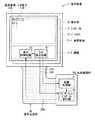
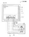
図1は、本発明の第一の実施の形態に係る表示装置1の全体構成を表すものである。本実施の形態の表示装置1は、表面に接触した物体(検出対称物)の接触情報などを読み取る入力機能を備えた表示装置である。この表示装置1は、表示部10と、表示部10とは別体に設けられた外部処理部20と、これらの間の信号を伝送する信号伝送部30とを備えている。なお、本発明の一実施の形態に係る入力装置は、上記表示装置1により具現化されるので、以下、合わせて説明する。[First embodiment]
FIG. 1 shows the overall configuration of a
表示部10は、I/Oパネル11(パネル)と、バックライト12とを備えている。I/Oパネル11は、複数の表示画素11Aおよび複数のセンサ素子11Bが一の面内に行方向および列方向に2次元配置されたものである。このI/Oパネル11は、表示画素11Aを介して画像情報を出力し、センサ素子11Bを介して外部からの情報入力を受け付ける入出力装置として機能する。バックライト12は、例えば、可視光領域の光をI/Oパネル11の背面へ向けて発する面発光源である。このバックライト12は、例えば、冷陰極管(CCFL;Cold Cathode Fluorescent Lamp)と呼ばれる冷陰極蛍光ランプや、発光ダイオード(LED;Light Emitting Diode)などを含んで構成されている。 The
ここで、表示画素11Aは、後述の表示制御回路13から印加される電圧の大きさに応じてバックライト12からの入射光を変調して出力するものである。この表示画素11Aは、例えば、赤色発光する赤色発光セルと、緑色発光する緑色発光セルと、青色発光する青色発光セルとを有している。各発光セルは、例えば、マトリクス状に配列された画素電極を有する画像表示側の透明基板と、ベタに形成された共通電極を有するバックライト側の透明基板との間に液晶層を設けた液晶表示パネルにおいて、各画素電極に対応する部分に相当する。 Here, the
一方、センサ素子11Bは、例えば、間隙を介して互いに対向する一対の電極を含む接触式のセンサであり、一対の電極が互いに接触することにより物体が表面に接触したことを検出するようになっている。このセンサ素子11Bは、例えば、上記した液晶表示パネルにおいて、透明基板上の画素電極、画素電極を駆動するTFT(Thin Film Transistor)、共通電極などと共に形成されている。 On the other hand, the
このI/O表示パネル11は、さらに、表示制御回路13(駆動回路)と、タッチ検出回路15(処理回路)とを有している。これらは、例えば、上記した液晶表示パネルにおいて、画像表示側の透明基板の表面のうち、センサ素子11BやTFTなどの形成されていない領域に形成されている。つまり、このI/Oパネル11には、表示画素11Aおよびセンサ素子11Bの形成された画素領域11−1と、表示制御回路13およびタッチ検出回路15の形成された回路領域11−2とが設けられている。 The I /
なお、表示制御回路13およびタッチ検出回路15が画像表示側の透明基板の表面にセンサ素子11BやTFTなどと共に形成されている場合には、これらが集積化されていることが好ましい。このようにした場合には、消費電力を低減することができるだけでなく、回路同士をつなぐ配線抵抗や信号波形のなまりを低減することができる。また、出力端子の数を減らすこともできるので、そのようにした場合には、信頼性が向上する。また、ノイズの影響を受けにくくなるので、より確実なセンシングが可能となる。 In the case where the
表示制御回路13は、複数の表示画素11Aを駆動することにより画素領域11−1に画像を表示させるものである。この表示制御回路13は、例えば、表示信号生成部、表示信号保持制御部、表示信号ドライバ、表示用スキャナなどを含んで構成されている(いずれも図示せず)。 The
表示信号生成部は、アプリケーションプログラム実行部22から供給された画像データ22Aに基づいて、例えば1画面ごと(1フィールドの表示ごと)に表示部10に表示するための表示信号を生成するものである。このようにして生成された表示信号が表示信号保持制御部へ出力される。 Based on the
表示信号保持制御部は、表示信号生成部から出力された表示信号を1画面ごとに、例えばSRAM(Static Random Access Memory)などからなるフィールドメモリに格納して保持するものである。この表示信号保持制御部はまた、各表示画素11Aを駆動する表示信号ドライバおよび表示用スキャナと、受光制御回路14とが連動して動作するように制御する役割も果たしている。 The display signal holding control unit stores and holds the display signal output from the display signal generating unit in a field memory such as an SRAM (Static Random Access Memory) for each screen. The display signal holding control unit also plays a role of controlling the display signal driver and display scanner for driving each
表示信号ドライバは、表示信号保持制御部から出力された1水平ライン分の表示データに対応する電圧を、駆動対象の表示画素11Aへ供給するものである。具体的には、表示信号ドライバは、表示信号保持制御部から出力される制御信号に応じて、表示信号ドライバと各表示画素11Aとを結ぶ信号線(図示せず)に、1水平ライン分の表示データに対応する電圧を供給することによって、駆動対象の表示画素11Aを駆動している。 The display signal driver supplies a voltage corresponding to display data for one horizontal line output from the display signal holding control unit to the
表示用スキャナは、表示信号保持制御部から出力された制御信号に応じて駆動対象の表示画素11Aを選択するものである。具体的には、表示用スキャナは、表示用スキャナと各表示画素11Aとを結ぶ走査線(図示せず)に走査信号を順次供給することによって、駆動対象の表示画素11Aを選択している。 The display scanner selects the
タッチ検出回路15は、センサ素子11Bから出力された出力信号11Cから、検出対称物についての要素情報(後述)を抽出するとともに、検出対称物の位置や接触面積などを特定する際に用いるシリアルデータ(後述)を導出するものである。 The
ここで、要素情報とは、検出対称物の位置や接触面積などの情報を得る際に必要となる基礎的な情報のことを指している。例えば、検出対称物の影響を受けた出力信号をオン信号としたときに、センサ素子11Bから入力されてきた出力信号11Cにオン信号に該当するものがあるか否かという判別情報が、上記した要素情報に含まれる。 Here, the element information refers to basic information necessary for obtaining information such as the position of the detection symmetry object and the contact area. For example, when the output signal affected by the detected symmetrical object is an ON signal, the discrimination information as to whether or not the
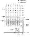
なお、図2では、出力信号11Cとしてオン信号を出力するオン状態のセンサ素子11Bを黒丸で表し、出力信号11Cとしてオフ信号(検出対称物の影響を受けなかった出力信号)を出力するオフ状態のセンサ素子11Bを白丸で表した。また、図2には、行方向および列方向に2次元配置されたセンサ素子11Bの画素領域11A上の位置を表現することを目的として、行方向の位置をYm+1、Ym+2、Ym+3、Ym+4、Ym+5、Ym+6、Ym+7、Ym+8(mは1以上の正数)と表現し、列方向の位置をSn+1、Sn+2、Sn+3、Sn+4、Sn+5、Sn+6(nは1以上の正数)と表現した。In FIG. 2, the
このタッチ検出回路15は、例えば、図2に示したように、変換回路16、並列入力直列出力回路17、判定回路18を含んで構成されている。 The
変換回路16は、センサ素子11Bから出力された出力信号11Cを二値化するアナログ−デジタル変換回路である。この変換回路16は、例えば、オン信号に該当する出力信号11Cを“1”に相当する信号に変換し、オフ信号に該当する出力信号11Cを“0”に相当する信号に変換するようになっている。二値化は、例えば、図2に例示したように、比較器(図中の三角の形をしたもの)に、出力信号11Cと、比較電位Vrefとを入力し、出力信号11Cが比較電位Vrefよりも大きい場合には出力信号16Aとして“1”に相当する信号を出力し、出力信号11Cが比較電位Vref以下である場合には、出力信号16Aとして“0”に相当する信号を出力することにより行われる。この変換回路16では、例えば、図2に示したように、センサ素子11Bから並列に入力された一群の出力信号11Cが一群の出力信号16Aに変換され、一群の出力信号16Aが並列に出力されている。The
並列入力直列出力回路17は、変換回路16から並列に出力された一群の出力信号16Aを直列(シリアルデータ)に変換して出力する回路である。このような回路は、例えば、図2に示したように、複数のDFF(Delay Flip-Flop)を用意し、一のDFFの一の入力と他のDFFの出力を互いに接続し、各DFFの他の入力と各変換回路16の出力端子を一つずつ別個に接続し、各DFFのクロック端子に共通のクロック線(Vck)を接続し、各DFFのリセット端子に共通のリセット線(Vrst)を接続することにより形成可能である。この回路では、最終段のDFFから、一群の出力信号16Aが一つずつ経時的に連続して(つまり直列に)出力信号17Aとして出力される。なお、本実施の形態では、この出力信号17Aが表示部10とは別体に設けられた外部処理部20に出力される。The parallel input
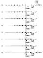
判定回路18は、並列入力直列出力回路17から順次入力される出力信号17Aにオン信号に該当するものがあるか否かを判定するものである。この判定回路18は、例えば、図2に示したように、並列入力直列出力回路17から順次入力される出力信号17Aのうち時間的な前後関係において互いに隣り合う2つの出力信号17Aのいずれか一方がオン信号に該当するか否かを判定するOR回路を含んで構成されている。 The
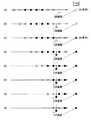
以下、図3(A)〜(H)に示した模式図を利用して、OR回路による判定方法について説明する。まず、一群の出力信号17(例えば図2の(Sn+3,y)に属する出力信号17)のうち、最右端のセンサ素子11Bから入力された出力信号17A(図3(A)の破線上に位置する白丸)と、初期値として用意された信号(図3(A)の横軸から外れた場所に位置する白丸)とに対してOR演算を行う。この場合、双方ともに白丸、つまり、オフ信号に該当するので、判定回路18は、出力信号18Aとしてオフ信号に対応する信号を出力する。Hereinafter, the determination method using the OR circuit will be described with reference to the schematic diagrams shown in FIGS. First, among the group of output signals 17 (for example, the
次に、一群の出力信号17(例えば図2の(Sn+3,y)に属する出力信号17)のうち、右から二番目のセンサ素子11Bから入力された出力信号17A(図3(B)の破線上に位置する白丸)と、先にOR演算により判定回路18から出力された信号(図3(B)の横軸から外れた場所に位置する白丸)とに対してOR演算を行う。この場合、双方ともに白丸、つまり、オフ信号に該当するので、判定回路18は、出力信号18Aとしてオフ信号に対応する信号を出力する。Next, among the group of output signals 17 (for example, the
次に、一群の出力信号17(例えば図2の(Sn+3,y)に属する出力信号17)のうち、右から三番目のセンサ素子11Bから入力された出力信号17A(図3(C)の破線上に位置する黒丸)と、先にOR演算により判定回路18から出力された信号(図3(C)の横軸から外れた場所に位置する白丸)とに対してOR演算を行う。この場合、一方が黒丸、つまり、オン信号に該当するので、判定回路18は、出力信号18Aとしてオン信号に対応する信号を出力する。Next, among the group of output signals 17 (for example, the
以後、同様にして、判定回路18は、図3(D)〜(H)に示したようにOR演算を行い、演算結果に対応した信号を出力信号18Aとして出力する。 Thereafter, similarly, the
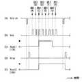
なお、上記のOR演算は、図4(A)〜(E)のような波形図でも説明することができる。ここで、図4(A)のVst−ckは、タッチ検出回路15における出力信号11Cの読み出し開始トリガであり、例えば、表示制御回路13からタッチ検出回路15へ入力される制御信号などに相当するものである。また、図4(B)のVckは、上述したDFFに接続されたクロック線からDFFに入力されるクロック信号である。図4(C)のVout1は、出力信号17Aの電圧である。図4(D)のVrstは、上述したDFFに接続されたリセット線からDFFに入力されるリセット信号である。なお、DFFに入力されるリセット信号は、判定回路18にも同時に入力されている(図2参照)。図4(E)のVout2は、出力信号18Aの電圧である。Note that the above OR operation can also be explained by waveform diagrams as shown in FIGS. Here, Vst-ck in FIG. 4 (A), a read start
図4(B)から、判定回路18は、Vckの波形の立ち上がりのタイミングで、図3(A)〜(G)で模式的に表したOR演算を行い、そのOR演算の結果に対応して、出力信号17A,18Aを変動させているのがわかる。なお、OR演算の性質上、出力信号18Aが一端オン信号に対応する電圧となると、それ以降はどのような出力信号17Aが判定回路18に入力されても、判定回路18は、出力信号18Aとしてオン信号に対応した電圧を出力してしまう。そのため、一群の出力信号17Aが新たに判定回路18に入力される前に、判定回路18にリセット信号を入力し、出力信号18Aをオフ信号に対応する電圧にしておくことが必要である。From FIG. 4B, the
このように、タッチ検出回路15は、全てのセンサ素子11Bからの出力信号11Cがタッチ検出回路15に入力される前に、既に入力された出力信号11Cからオン信号の有無を判別し、その判別結果を出力信号18Aとして出力している。また、このタッチ検出回路15は、複数のセンサ素子11Bのうち一の行に配置された全てのセンサ素子11Bの出力信号11Cから得られた出力信号17Aが一つずつ直列に入力される度に、判別結果を出力信号18Aとして出力している。 As described above, the
外部処理部20は、画像処理部21と、アプリケーションプログラム実行部22とを有している。 The
画像処理部21は、タッチ検出回路15から入力された出力信号17A(シリアルデータ)に対して所定の信号処理を行うことにより、検出対称物の位置や接触面積などを特定するものである。検出対称物の位置は、例えば、出力信号17Aを画素領域11A上の座標に対応した画像情報(例えばビットマップデータ)に変換し、変換した画像情報を利用して、中心座標(または重心座標)を抽出する演算を行うことにより導出することが可能である。また、中心座標(または重心座標)が複数導出された場合には、例えば、導出された中心座標(または重心座標)ごとにラベリング処理がなされる。接触面積については、例えば、上述した画像情報を利用して、外縁座標を抽出し、外縁で囲まれた領域の面積を算出することにより得られる。このようにして導出された情報は、タッチ情報21Aとして画像処理部21からアプリケーションプログラム実行部22へ出力される。 The
アプリケーションプログラム実行部22は、所定のアプリケーションプログラムに応じた処理を実行するものであり、例えば、画像処理部21からの出力(タッチ情報21A)に基づいて、画像データ22Aに所定のデータを重畳したり、画像データ22Aを新たなデータに置き換えたりするものである。このアプリケーションプログラム実行部22は、例えば、所定のプログラムを実行する1または複数のプロセッサによって構成されていている。 The application
このアプリケーションプログラム実行部22では、タッチ検出回路15からの出力信号18Aの入力をトリガとして所定の処理が開始される。例えば、画像処理部21から何も入力がない間、画像処理部21からの出力(タッチ情報21A)に基づいて処理を実行する部分に対応する部分(プロセッサ)がスリープしており、タッチ検出回路15からの出力信号18Aの入力をトリガとしてウェイクアップするようになっていてもよい。このようにした場合には、消費電力の低減を図ることができる。 In the application
信号伝送部30は、表示部10と外部処理部20との間の信号を伝送するものであり、例えば、フレキシブルプリント配線板(FPC)によって構成されている。FPCは、例えば、一の方向に延在する帯状のベースフィルムを有している。ベースフィルムの一端には、表示部10のコネクタ(図示せず)と接続するコネクタ(図示せず)が設けられており、ベースフィルムの他端には、外部処理部20のコネクタ(図示せず)と接続するコネクタ(図示せず)が設けられている。ベースフィルムの表面には、ベースフィルムの両端に設けられた双方のコネクタに接続された配線(図示せず)が設けられている。さらに、この信号伝送部30には、ベースフィルム上の配線を保護するカバーレイ(図示せず)が設けられている。 The
次に、本実施の形態の表示装置1の動作の一例について説明する。 Next, an example of operation | movement of the
この表示装置1では、アプリケーションプログラム実行部22から供給される画像データ22Aに基づいて、表示制御回路13内の表示信号ドライバにおいて表示用の駆動信号が出力されると共に、表示制御回路13内の表示用スキャナにおいて線順次駆動がなされ、表示面に画像が表示される。このとき、受光制御回路14内の受光用ドライバにおいて受光用の駆動信号が出力されると共に、受光制御回路14内の受光用スキャナにおいて線順次駆動がなされ、画像が撮像される。 In the
そして、タッチ検出回路15において、センサ素子11Bから出力された出力信号11Cに基づいて、検出対称物の位置や接触面積などの情報を導出するにあたっての前処理的な信号処理が行われる。その結果、複数のセンサ素子11Bのうち一の行に配置された全てのセンサ素子11Bからの出力信号11Cが一つずつ直列に入力される度に、タッチ検出回路15から、出力信号17A(シリアルデータ)および出力信号18A(判定結果)がほぼ同時に出力される。 Then, the
続いて、画像処理部21において、検出対称物の位置や接触面積などを特定する処理が開始されるとほぼ同時に、アプリケーションプログラム実行部22において、タッチ検出回路15からの出力信号18Aの入力をトリガとして所定の処理が開始される。例えば、画像処理部21からの出力(タッチ情報21A)に基づいて処理を実行する部分に対応するプロセッサがタッチ検出回路15からの出力信号18Aの入力をトリガとしてウェイクアップする。これにより、そのあと画像処理部21からの出力(タッチ情報21A)が入力された時には、画像処理部21からの出力(タッチ情報21A)に基づいて処理を実行する部分に対応する部分(プロセッサ)は既にウェイクアップしており、タッチ情報21Aに基づいた処理を直ちに実行することができる。 Subsequently, when the
このように、本実施の形態では、I/Oパネル11内に設けられたタッチ検出回路15において、全てのセンサ素子11Bからの出力信号11Cが入力される前に出力信号18A(判定結果)が出力される。これにより、例えば、全てのセンサ素子11Bの出力信号11Cから得られた出力信号17A(シリアルデータ)がI/Oパネル11とは別体で設けられた外部処理部20に入力される前に、出力信号18A(判定結果)を外部処理部20に入力することが可能となる。その結果、例えば、出力信号18A(判定結果)を利用した所定の処理をアプリケーションプログラム実行部22で開始したり、出力信号18A(判定結果)をトリガとして、アプリケーションプログラム実行部22のうちスリープしている部分(プロセッサ)をウェイクアップさせたりするなどの前処理を早期に開始することができる。したがって、前処理を早期に開始した分だけ、表示面に物体が接触してから、後段の処理回路(アプリケーションプログラム実行部22)における主たる演算処理の実行開始までに要する時間を短縮することができ、レイテンシを速くすることができる。 Thus, in the present embodiment, in the
なお、本実施の形態では、センサ素子11Bのスキャン速度を速くする必要がないので、検出のための信号線や走査線を設ける必要がなく、レイテンシの改善に伴って表示性能が低下する虞はない。したがって、表示性能を低下させることなく、レイテンシを速くすることができる。 In this embodiment, since it is not necessary to increase the scanning speed of the
[変形例]
上記実施の形態では、タッチ検出回路15は、複数のセンサ素子11Bのうち一の行に配置された全てのセンサ素子11Bの出力信号11Cから得られた出力信号17Aが一つずつ直列に入力される度に、判別結果を出力信号18Aとして出力していたが、他のタイミングで、判別結果を出力信号18Aとして出力することも可能である。他のタイミングで、判別結果を出力信号18Aとして出力するためには、例えば、図5に示したように、判定回路18の出力段に、スイッチ素子18Bを設ければよい。そのようにした場合に、例えば、図6(A)〜(H)、図7(A)〜(E)に示したように、複数のセンサ素子11Bのうち一の行に配置された全てのセンサ素子11Bの出力信号から得られた出力信号17Aが全て入力されたのちに、スイッチ素子18Bを、スイッチ素子18Bに接続されたクロック線に印加する信号Vsr−ckをオンオフし、信号Vsr−ckのオンオフに同期して、判別結果を出力信号18Aとして出力してもよい。[Modification]
In the above embodiment, the
また、上記実施の形態および上記変形例では、判定回路18は、OR回路を含んで構成されていたが、例えば、並列入力直列出力回路17から順次入力される出力信号17Aのうち時間的な前後関係において互いに隣り合う2つの出力信号17Aの双方がオン信号に該当するか否かを判定するAND回路を含んで構成されていてもよい。 In the embodiment and the modification, the
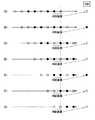
以下、図8(A)〜(G)に示した模式図を利用して、AND回路による判定方法について説明する。まず、一群の出力信号17のうち、最右端のセンサ素子11Bから入力された出力信号17A(図8(A)の破線上に位置する白丸)と、一群の出力信号17のうち、右から二番目のセンサ素子11Bから入力された出力信号17A(図8(A)の破線の左隣に位置する黒丸)とに対してAND演算を行う。この場合、一方だけが黒丸、つまり、オン信号に該当するので、判定回路18は、出力信号18Aとしてオフ信号に対応する信号を出力する。 Hereinafter, a determination method using an AND circuit will be described with reference to the schematic diagrams shown in FIGS. First, out of a group of output signals 17, an
次に、一群の出力信号17のうち、右から二番目のセンサ素子11Bから入力された出力信号17A(図8(B)の破線上に位置する黒丸)と、右から三番目のセンサ素子11Bから入力された出力信号17A(図8(B)の破線の左隣に位置する黒丸)とに対してAND演算を行う。この場合、双方ともに黒丸、つまり、オン信号に該当するので、判定回路18は、出力信号18Aとしてオン信号に対応する信号を出力する。 Next, among the group of output signals 17, the
以後、同様にして、判定回路18は、図8(C)〜(G)に示したようにAND演算を行い、演算結果に対応した信号を出力信号18Aとして出力する。 Thereafter, similarly, the
[第二の実施の形態]
図9は、本発明の第二の実施の形態に係る表示装置2の全体構成を表すものである。この表示装置2は、表示部10にタッチ検出回路45を有している点で、表示部10にタッチ検出回路15を有する表示装置1の構成と相違する。そこで、以下では、上記実施の形態との相違点について主に説明し、上記実施の形態との共通点についての説明を適宜省略するものとする。[Second Embodiment]
FIG. 9 shows the overall configuration of the
タッチ検出回路45は、例えば、図10に示したように、変換回路16、並列入力直列出力回路47、判定回路48を含んで構成されている。 The
並列入力直列出力回路47は、上記実施の形態の並列入力直列出力回路17と同様、変換回路16から並列に出力された一群の出力信号16Aを直列(シリアルデータ)に変換して出力する回路である。しかし、この並列入力直列出力回路47は、複数のセンサ素子11Bのうち互いに隣接する2つの行に配置された全てのセンサ素子11Bの出力信号11Cから得られた出力信号47Aを2×2のマトリクスで後段の判定回路48に出力することができるように構成されている。 The parallel input
具体的には、並列入力直列出力回路47は、上記実施の形態の並列入力直列出力回路17の後段に、1入力1出力のDFFを、前段に含まれる2入力2出力のDFFの数と同じ数だけ直列に接続して構成されている。さらに、前段の最後に設けられたDFFの出力端子と、前段の最後から二番目に設けられたDFFの出力端子と、後段の最後に設けられたDFFの出力端子と、後段の最後から二番目に設けられたDFFの出力端子とが並列入力直列出力回路47の出力端子となっている。そして、それら4つの出力端子が、判定回路48の4つの入力端子に一つずつ接続されている。また、後段の最後に設けられたDFFの出力端子は、タッチ検出回路45の出力端子の一つとなっており、画像処理部21の入力端子と信号伝送部30を介して接続されている。 Specifically, the parallel input
なお、前段の2入力2出力のDFFについては、各DFFのクロック端子に共通のクロック線(Vck1)が接続され、1入力1出力のDFFについては、各DFFのクロック端子に共通のクロック線(Vck2)が接続されている。また、1入力1出力のDFFには、前段の2入力2出力のDFFと同様、各DFFのリセット端子に共通のリセット線(Vrst)が接続されている。Note that a common clock line (Vck1 ) is connected to the clock terminal of each DFF for the two-input two-output DFF in the previous stage, and a clock line common to the clock terminal of each DFF for the one-input one-output DFF. (Vck2 ) is connected. In addition, a common reset line (Vrst ) is connected to the reset terminal of each DFF, similarly to the two-input two-output DFF in the previous stage, to the one-input one-output DFF.
判定回路48は、並列入力直列出力回路47から2×2のマトリクスで順次入力される出力信号47Aにオン信号に該当するものがあるか否かを判定するものである。この判定回路48は、例えば、図10に示したように、並列入力直列出力回路47から2×2のマトリクスで順次入力される出力信号47Aのうち2×2のマトリクスにおいて互いに隣り合う2つの出力信号17Aの双方がオン信号に該当するか否かを判定する回路を含んで構成されている。なお、図10には、2×2のマトリクスにおいて斜め方向についても互いに隣り合う2つの出力信号17Aの双方がオン信号に該当するか否かを判定する回路の構成例が示されているが、必要に応じて、2×2のマトリクスにおける斜め方向の判定に用いる回路部分をなくしてもよい。 The determination circuit 48 determines whether or not there is an
以下、図11(A)〜(G)に示した模式図を利用して、上記した回路による判定方法について説明する。まず、一群の出力信号47(例えば図10の(Sn+3,y)および(Sn+4,y)に属する出力信号47)のうち、最右端のセンサ素子11Bから入力された出力信号47A(図11(A)の方形状の破線内の右側に位置する2つの白丸)と、一群の出力信号47(例えば図10の(Sn+3,y)および(Sn+4,y)に属する出力信号47)のうち、右から二番目のセンサ素子11Bから入力された出力信号47A(図11(A)の方形状の破線内の左側に位置する2つの白丸)とに対して上述した演算を行う。この場合、4つとも白丸、つまり、オフ信号に該当するので、判定回路48は、出力信号48Aとしてオフ信号に対応する信号を出力する。Hereinafter, the determination method using the above-described circuit will be described with reference to the schematic diagrams shown in FIGS. First, out of a group of output signals 47 (for example, output signals 47 belonging to (Sn + 3 , y) and (Sn + 4 , y) in FIG. 10), an
次に、一群の出力信号47(例えば図10の(Sn+3,y)および(Sn+4,y)に属する出力信号47)のうち、右から二番目のセンサ素子11Bから入力された出力信号47A(図11(B)の方形状の破線内の右側に位置する2つの白丸)と、一群の出力信号47(例えば図10の(Sn+3,y)および(Sn+4,y)に属する出力信号47)のうち、右から三番目のセンサ素子11Bから入力された出力信号47A(図11(A)の方形状の破線内の左側に位置する2つの黒丸)とに対して上述した演算を行う。この場合、左側の2つの出力信号47Aが共に黒丸、つまり、オン信号に該当するので、判定回路48は、出力信号48Aとしてオン信号に対応する信号を出力する。Next, among the group of output signals 47 (for example, the output signals 47 belonging to (Sn + 3 , y) and (Sn + 4 , y) in FIG. 10), the
以後、同様にして、判定回路48は、図11(C)〜(G)に示したように、上述の演算を行い、演算結果に対応した信号を出力信号48Aとして出力する。 Thereafter, similarly, as shown in FIGS. 11C to 11G, the determination circuit 48 performs the above-described calculation and outputs a signal corresponding to the calculation result as the
このように、タッチ検出回路45は、全てのセンサ素子11Bからの出力信号11Cがタッチ検出回路45に入力される前に、既に入力された出力信号11Cからオン信号の有無を判別し、その判別結果を出力信号48Aとして出力している。また、このタッチ検出回路45は、複数のセンサ素子11Bのうち2つの行に配置された全てのセンサ素子11Bの出力信号11Cから得られた出力信号47Aが2×2のマトリクスで入力される度に、判別結果を出力信号48Aとして出力している。 As described above, the
外部処理部20は、上記実施の形態と同様、画像処理部21と、アプリケーションプログラム実行部22とを有している。画像処理部21は、タッチ検出回路45から入力された出力信号47A(シリアルデータ)に対して所定の信号処理を行うことにより、表示面に接触あるいは近接する物体(検出対称物)の位置や接触面積などを特定するものである。また、アプリケーションプログラム実行部22では、タッチ検出回路45からの出力信号48Aの入力をトリガとして所定の処理が開始される。例えば、画像処理部21から何も入力がない間、画像処理部21からの出力(タッチ情報21A)に基づいて処理を実行する部分に対応するプロセッサがスリープしており、タッチ検出回路45からの出力信号48Aの入力をトリガとしてウェイクアップするようになっていてもよい。 The
次に、本実施の形態の表示装置2の動作の一例について説明する。 Next, an example of operation | movement of the
この表示装置2では、アプリケーションプログラム実行部22から供給される画像データ22Aに基づいて、表示制御回路13内の表示信号ドライバにおいて表示用の駆動信号が出力されると共に、表示制御回路13内の表示用スキャナにおいて線順次駆動がなされ、表示面に画像が表示される。このとき、受光制御回路14内の受光用ドライバにおいて受光用の駆動信号が出力されると共に、受光制御回路14内の受光用スキャナにおいて線順次駆動がなされ、画像が撮像される。 In the
そして、タッチ検出回路45において、センサ素子11Bから出力された出力信号11Cに基づいて、検出対称物の位置や接触面積などの情報を導出するにあたっての前処理的な信号処理が行われる。その結果、複数のセンサ素子11Bのうち一の行に配置された全てのセンサ素子11Bからの出力信号11Cが2×2のマトリクスで入力される度に、タッチ検出回路45から、出力信号47A(シリアルデータ)および出力信号48A(判定結果)がほぼ同時に出力される。 Then, in the
続いて、画像処理部21において、検出対称物の位置や接触面積などを特定する処理が開始されるとほぼ同時に、アプリケーションプログラム実行部22において、タッチ検出回路45からの出力信号48Aの入力をトリガとして所定の処理が開始される。例えば、画像処理部21からの出力(タッチ情報21A)に基づいて処理を実行する部分に対応するプロセッサがタッチ検出回路45からの出力信号48Aの入力をトリガとしてウェイクアップする。これにより、そのあと画像処理部21からの出力(タッチ情報21A)が入力された時には、画像処理部21からの出力(タッチ情報21A)に基づいて処理を実行する部分に対応するプロセッサは既にウェイクアップしており、タッチ情報21Aに基づいた処理を直ちに実行することができる。 Subsequently, almost simultaneously with the start of the process of specifying the position and contact area of the detected object in the
このように、本実施の形態では、I/Oパネル11内に設けられたタッチ検出回路45において、全てのセンサ素子11Bからの出力信号11Cが入力される前に出力信号48A(判定結果)が出力される。これにより、例えば、全てのセンサ素子11Bの出力信号11Cから得られた出力信号47A(シリアルデータ)がI/Oパネル11とは別体で設けられた外部処理部20に全て入力される前に、出力信号48A(判定結果)を外部処理部20に入力することが可能となる。その結果、例えば、出力信号48A(判定結果)を利用した所定の処理をアプリケーションプログラム実行部22で開始したり、出力信号48A(判定結果)をトリガとして、アプリケーションプログラム実行部22のうちスリープしている部分をウェイクアップさせたりするなどの前処理を早期に開始することができる。したがって、前処理を早期に開始した分だけ、表示面に物体が接触してから、後段の処理回路(アプリケーションプログラム実行部22)における主たる演算処理の実行開始までに要する時間を短縮することができ、レイテンシを速くすることができる。 As described above, in the present embodiment, the
なお、本実施の形態においても、センサ素子11Bのスキャン速度を速くする必要がないので、検出のための信号線や走査線を設ける必要がなく、レイテンシの改善に伴って表示性能が低下する虞はない。したがって、表示性能を低下させることなく、レイテンシを速くすることができる。 Also in this embodiment, since it is not necessary to increase the scanning speed of the
[変形例]
上記第二の実施の形態では、並列入力直列出力回路47は、複数のセンサ素子11Bのうち互いに隣接する2つの行に配置された全てのセンサ素子11Bの出力信号11Cから得られた出力信号47Aを2×2のマトリクスで後段の判定回路48に出力するようになっていた。しかし、並列入力直列出力回路47は、出力信号47Aを3×3のマトリクスで後段の判定回路48に出力するようになっていてもよい。ただし、その場合には、判定回路48は、例えば、並列入力直列出力回路47から3×3のマトリクスで順次入力される出力信号47Aのうち3×3のマトリクスにおいて互いに隣り合う3つの出力信号17Aの全てがオン信号に該当するか否かを判定する回路を含んで構成されていることが好ましい。[Modification]
In the second embodiment, the parallel input
以上、実施の形態およびその変形例を挙げて本発明を説明したが、本発明は実施の形態等に限定されるものではなく、種々の変形が可能である。 Although the present invention has been described with reference to the embodiment and its modifications, the present invention is not limited to the embodiment and the like, and various modifications can be made.
例えば、上記各実施の形態等では、タッチ検出回路15において抽出される要素情報として判別情報だけしか挙げられていなかったが、それ以外のものについてもタッチ検出回路15において抽出することは可能である。 For example, in each of the above-described embodiments and the like, only the discrimination information is listed as element information extracted by the
例えば、複数のセンサ素子11Bのうち少なくとも一の行に配置された全てのセンサ素子11Bからの出力信号11Cの中にオン信号に該当するものがいくつ含まれているかという個数についての情報をタッチ検出回路15において抽出してもよい。また、要素情報には、例えば、複数のセンサ素子11Bのうち少なくとも一の行に配置された全てのセンサ素子11Bからの出力信号11Cのうち、オン信号に該当する出力信号11Cを出力したセンサ素子11Bの位置についての情報をタッチ検出回路15において抽出してもよい。なお、二番目に挙げた情報には、例えば、一群の出力信号11Cのうち最初にオン信号に該当すると検出された出力信号11Cを出力したセンサ素子11Bの位置(開始点)や、開始点を検出した後、オフ信号(検出対称物の影響を受けなかった出力信号)を検出する1つ前にオン信号に該当すると検出された出力信号11Cを出力したセンサ素子11Bの位置(終了点)、開始点と終了点との距離(両端間の幅)などが含まれ得る。なお、オン信号の個数情報、開始点または終了点の情報、および両端間の幅の情報を用いることにより、出力信号17Aを画素領域11A上の座標に対応した画像情報(例えばビットマップデータ)を再構成することも可能である。 For example, information on the number of
また、上記各実施の形態等では、センサ素子11Bが接触式のセンサである場合について説明したが、例えば、フォトダイオードなどの受光式のセンサであってもよい。この場合には、物体が表面に接触した場合だけでなく、表面に近接した場合にも物体を検出することが可能であり、例えば、表面に接触した指の指紋や静脈情報を読み取ったりすることも可能となる。なお、センサ素子11Bが受光式のセンサである場合には、センサ素子11Bを制御する受光制御回路(図示せず)を画素領域11Aに設けることが好ましい。 In each of the above-described embodiments, the case where the
また、上記実施の形態では、表示部10は、バックライト12上に液晶表示パネルを含むI/Oパネル11を備えている場合について説明していたが、表示部10が、互いに対向する透明基板の間に有機層を設けた有機ELパネルのように、画素を構成する表示素子自体が発光する自発光型パネルを備えていてもよい。 In the above embodiment, the case where the
1,2…表示装置、10…表示部、11−1…画素領域、11−2…回路領域、11A…表示画素、11B…センサ素子、11C,16A,17A,18A,47A,48A…出力信号、12…バックライト、13…表示制御回路、15,45…タッチ検出回路、16…変換回路、17,47…並列入力直列出力回路、18,48…判定回路、18A…スイッチ回路、20…外部処理部、21…画像処理部、22…アプリケーションプログラム実行部、30…信号伝送部。 DESCRIPTION OF
Claims (6)
Translated fromJapanese所定の処理単位の前記複数のセンサ素子の出力信号を並列に入力し、前記パネルの表面に接触または近接する物体の影響を受けたときの出力信号をオン信号とする二値化処理を行う変換回路と、
前記変換回路から並列に出力された前記処理単位の二値化信号を直列に変換し、変換した直列信号を、所定の領域に配置される前記複数のセンサ素子に対応する前記直列信号がすべて入力されてから信号処理を開始する処理部に順次出力する並列入力直列出力回路と、
前記並列入力直列出力回路から前記直列信号を順次入力し、前記処理単位ごとに、前記直列信号が入力される度に当該直列信号を含む既に入力された前記直列信号に前記オン信号が含まれていたか否かを判別し、その判別結果を出力する判定回路と、
を有する入力装置。A plurality of sensor elements arranged two-dimensionally in rows and columns, a driving circuit for driving the plurality of sensorelements,the panelis provided,
Conversion for performing binarization processing byinputting the output signals of the plurality of sensor elements in a predetermined processing unit in parallel and usingthe output signal as an ON signalwhen influenced by an object in contact with or close to the surface of the panelCircuit ,
The binarized signals of the processing units output in parallel from the conversion circuit are converted in series, and all the serial signals corresponding to the plurality of sensor elements arranged in a predetermined region are input to the converted serial signal. A parallel input serial output circuit that sequentially outputs to a processing unit that starts signal processing after being
The serial signal is sequentially input from the parallel input serial output circuit, and the ON signalis included in thealready input serial signal including the serial signal every time the serial signal is input for each processing unit. Adetermination circuit that determineswhether or not and outputs the determination result;
An input device.
前記処理単位ごとに、入力された前記直列信号と前回の判別結果との論理和を演算し、判別結果を更新する論理和回路と、
前記論理和回路が更新した判別結果を前記前回の判別結果として保持するとともに、前記処理単位の最初の直列信号が入力されたときに、保持していた前記前回の判別結果をリセットする保持回路と、
を有し、
前記直列信号が一つずつ入力される度に、前記判別結果を出力する、請求項1に記載の入力装置。Thedetermination circuit includes:
A logical sum circuit that calculates the logical sum of the input serial signal and the previous determination result for each processing unit, and updates the determination result;
A holding circuit that holds the determination result updated by the OR circuit as the previous determination result, and resets the previous determination result that was held when the first serial signal of the processing unit is input; ,
Have
Everytime the serial signal is input one by one, and outputs the determinationresult, the input device according to claim 1.
前記所定の条件が成立されたのちに、前記判別結果として前記論理和回路の出力信号を出力する請求項2に記載の入力装置。Thedetermination circuit includesa switch element that inputs an output signal of the logical sum circuit and an off signal, and outputs the output signal of the logical sum circuit or the off signal according to a predetermined condition,
The input device according to claim2 , wherein after thepredetermined condition is satisfied ,an output signal of theOR circuit is output as the determination result.
前記パネルと前記外部処理部との間の信号を伝送する信号伝送部と、
を備え、
前記外部処理部は、前記判定回路から出力される前記判別結果を取得し、前記判別結果に基づき、前記オン信号の検出をトリガとして所定の処理を開始する、請求項1ないし請求項3の少なくとも一項に記載の入力装置。An external processing unit provided separately from the panel;
A signal transmission unit for transmitting a signal between the panel and the external processing unit;
With
The at least one of claims 1 to 3,wherein the external processing unitacquires the determination resultoutput from the determination circuit,and starts predetermined processing based on the determination result with the detection of the ON signal as a trigger. The input device according toone item .
所定の処理単位の前記複数のセンサ素子の出力信号を並列に入力し、前記パネルの表面に接触または近接する物体の影響を受けたときの出力信号をオン信号とする二値化処理を行う変換回路と、
前記変換回路から並列に出力された前記処理単位の二値化信号を直列に変換し、変換した直列信号を、所定の領域に配置される前記複数のセンサ素子に対応する前記直列信号がすべて入力されてから信号処理を開始する処理部に順次出力する並列入力直列出力回路と、
前記並列入力直列出力回路から前記直列信号を順次入力し、前記処理単位ごとに、前記直列信号が入力される度に当該直列信号を含む既に入力された前記直列信号に前記オン信号が含まれていたか否かを判別し、その判別結果を出力する判定回路と、
を有する表示装置。A plurality of display pixels and a plurality of sensor elements arranged two-dimensionally in rows and columns,a panel in which a driving circuit for driving the plurality of display pixels and the plurality of sensorelements, are provided,
Conversion for performing binarization processing by inputting the output signals of the plurality of sensor elements in a predetermined processing unit in parallel and using the output signal as an ON signal when influenced by an object in contact with or close to the surface of the panel Circuit,
The binarized signals of the processing units output in parallel from the conversion circuit are converted in series, and all the serial signals corresponding to the plurality of sensor elements arranged in a predetermined region are input to the converted serial signal. A parallel input serial output circuit that sequentially outputs to a processing unit that starts signal processing after being
The serial signal is sequentially input from the parallel input serial output circuit, and the ON signal is included in the already input serial signal including the serial signal every time the serial signal is input for each processing unit. A determination circuit that determines whether or not and outputs the determination result;
A display device.
Priority Applications (4)
| Application Number | Priority Date | Filing Date | Title |
|---|---|---|---|
| JP2008256060AJP5252427B2 (en) | 2008-10-01 | 2008-10-01 | Input device and display device |
| TW098130137ATWI404999B (en) | 2008-10-01 | 2009-09-07 | Input device and display |
| US12/557,289US20100079394A1 (en) | 2008-10-01 | 2009-09-10 | Input device and display |
| CN2009101794182ACN101714038B (en) | 2008-10-01 | 2009-10-09 | Input device and display |
Applications Claiming Priority (1)
| Application Number | Priority Date | Filing Date | Title |
|---|---|---|---|
| JP2008256060AJP5252427B2 (en) | 2008-10-01 | 2008-10-01 | Input device and display device |
Publications (2)
| Publication Number | Publication Date |
|---|---|
| JP2010086377A JP2010086377A (en) | 2010-04-15 |
| JP5252427B2true JP5252427B2 (en) | 2013-07-31 |
Family
ID=42056874
Family Applications (1)
| Application Number | Title | Priority Date | Filing Date |
|---|---|---|---|
| JP2008256060AExpired - Fee RelatedJP5252427B2 (en) | 2008-10-01 | 2008-10-01 | Input device and display device |
Country Status (4)
| Country | Link |
|---|---|
| US (1) | US20100079394A1 (en) |
| JP (1) | JP5252427B2 (en) |
| CN (1) | CN101714038B (en) |
| TW (1) | TWI404999B (en) |
Families Citing this family (11)
| Publication number | Priority date | Publication date | Assignee | Title |
|---|---|---|---|---|
| US8963852B2 (en)* | 2010-08-20 | 2015-02-24 | Innolux Corporation | Touch panel, driving method for the touch panel, program for getting touch information, and memory media |
| KR101329461B1 (en)* | 2010-11-25 | 2013-11-15 | 엘지디스플레이 주식회사 | Display device having touch screen panel |
| US9015682B1 (en) | 2012-03-28 | 2015-04-21 | Google Inc. | Computer code transformations to create synthetic global scopes |
| US20150205585A1 (en)* | 2012-06-04 | 2015-07-23 | Google Inc. | Delayed compiling of scripting language code |
| US9383840B2 (en)* | 2013-04-22 | 2016-07-05 | Samsung Display Co., Ltd. | Method and apparatus to reduce display lag using image overlay |
| TWI507957B (en)* | 2013-07-22 | 2015-11-11 | Chunghwa Picture Tubes Ltd | Method of driving touch display and touch display capable of increasing signal-to-noise ratio |
| US9857394B2 (en) | 2013-10-04 | 2018-01-02 | Microchip Technology Incorporated | Multiple channel capacitive voltage divider scanning method and apparatus |
| KR102171389B1 (en)* | 2014-04-21 | 2020-10-30 | 삼성디스플레이 주식회사 | Image display system |
| KR102206047B1 (en) | 2014-09-15 | 2021-01-21 | 삼성디스플레이 주식회사 | Terminal and apparatus and method for reducing display lag |
| CA2965351A1 (en)* | 2014-11-18 | 2016-05-26 | Tactual Labs Co. | System and method for inter-module communication |
| CN107238742A (en)* | 2017-04-24 | 2017-10-10 | 天津瑞能电气有限公司 | MW class micro-capacitance sensor and off-network switching transient state monitoring system |
Family Cites Families (11)
| Publication number | Priority date | Publication date | Assignee | Title |
|---|---|---|---|---|
| JPS5920348U (en)* | 1982-07-28 | 1984-02-07 | オムロン株式会社 | Transparent finger touch input device |
| JPS63172325A (en)* | 1987-01-10 | 1988-07-16 | Pioneer Electronic Corp | Touch panel controller |
| JP2866575B2 (en)* | 1994-03-28 | 1999-03-08 | 日立ソフトウエアエンジニアリング株式会社 | Pressure-sensitive tablet and information processing device |
| JP3379873B2 (en)* | 1996-04-05 | 2003-02-24 | 株式会社デジタル | Matrix type touch panel input device |
| JP2001075074A (en)* | 1999-08-18 | 2001-03-23 | Internatl Business Mach Corp <Ibm> | Touch sensor type liquid crystal display device |
| US7100141B1 (en)* | 2003-12-23 | 2006-08-29 | Altera Corporation | Technology mapping technique for fracturable logic elements |
| KR101160828B1 (en)* | 2004-12-23 | 2012-06-29 | 삼성전자주식회사 | Display device, driving method thereof, and driving apparatus for display device |
| KR101171185B1 (en)* | 2005-09-21 | 2012-08-06 | 삼성전자주식회사 | Touch sensible display device and driving apparatus and method thereof |
| JP2007128497A (en)* | 2005-10-05 | 2007-05-24 | Sony Corp | Display apparatus and method thereof |
| US20070182723A1 (en)* | 2006-01-31 | 2007-08-09 | Toshiba Matsushita Display Technology Co., Ltd. | Display device |
| KR101303881B1 (en)* | 2006-08-03 | 2013-09-04 | 삼성디스플레이 주식회사 | Touch screen and method of manufacturing the same, and display having the same |
- 2008
- 2008-10-01JPJP2008256060Apatent/JP5252427B2/ennot_activeExpired - Fee Related
- 2009
- 2009-09-07TWTW098130137Apatent/TWI404999B/ennot_activeIP Right Cessation
- 2009-09-10USUS12/557,289patent/US20100079394A1/ennot_activeAbandoned
- 2009-10-09CNCN2009101794182Apatent/CN101714038B/ennot_activeExpired - Fee Related
Also Published As
| Publication number | Publication date |
|---|---|
| CN101714038A (en) | 2010-05-26 |
| JP2010086377A (en) | 2010-04-15 |
| TWI404999B (en) | 2013-08-11 |
| US20100079394A1 (en) | 2010-04-01 |
| CN101714038B (en) | 2012-11-07 |
| TW201022781A (en) | 2010-06-16 |
Similar Documents
| Publication | Publication Date | Title |
|---|---|---|
| JP5252427B2 (en) | Input device and display device | |
| CN108664895B (en) | Display device and fingerprint identification method thereof | |
| US8797275B2 (en) | Display apparatus and image pickup apparatus | |
| JP2004318819A (en) | Display device and information terminal device | |
| US8390578B2 (en) | Sensing device, display device, electronic apparatus, and sensing method | |
| EP2889674A1 (en) | Built-in capacitive touch screen crystal display module and driving method thereof | |
| US10754471B2 (en) | Touch sensing device and image display device using the same | |
| CN106897696A (en) | A kind of lines identification module, its driving method and display device | |
| JP2008198211A (en) | Display device and driving method thereof | |
| JP2009217461A (en) | Display device and method of detecting position | |
| CN112052715A (en) | Providing a light source in a display panel and performing optical fingerprint recognition using the same | |
| CN102687102A (en) | Display device with optical sensor | |
| TWI614652B (en) | Display panel having built-in touchscreen and touch display device including the same | |
| JP2008059254A (en) | Display imaging apparatus, information input device, object detection program and object detection method | |
| CN112346588B (en) | Touch detection method, driver and touch display device | |
| JP2009193482A (en) | Sensing device, display device, electronic device, and sensing method | |
| CN111797673A (en) | Drive device and method of operation | |
| CN103412673A (en) | Colored film substrate, manufacturing method of colored film substrate and touch screen | |
| KR20150070664A (en) | Display device with integrated touch screen | |
| CN111651083B (en) | Control method and control device for touch display screen and display equipment | |
| CN107958650B (en) | Biological sensing module, driving circuit thereof and electronic equipment | |
| KR20220150970A (en) | Electronic device with fingerprint sensing function | |
| KR101723879B1 (en) | Display device with integrated touch screen | |
| CN209708138U (en) | Biological sensing mould group and its driving circuit, electronic equipment | |
| US20160117040A1 (en) | Touch display apparatus and method for detecting touch point thereof |
Legal Events
| Date | Code | Title | Description |
|---|---|---|---|
| A621 | Written request for application examination | Free format text:JAPANESE INTERMEDIATE CODE: A621 Effective date:20110926 | |
| A711 | Notification of change in applicant | Free format text:JAPANESE INTERMEDIATE CODE: A711 Effective date:20120330 | |
| A977 | Report on retrieval | Free format text:JAPANESE INTERMEDIATE CODE: A971007 Effective date:20120718 | |
| A131 | Notification of reasons for refusal | Free format text:JAPANESE INTERMEDIATE CODE: A131 Effective date:20120724 | |
| A521 | Written amendment | Free format text:JAPANESE INTERMEDIATE CODE: A523 Effective date:20120919 | |
| TRDD | Decision of grant or rejection written | ||
| A01 | Written decision to grant a patent or to grant a registration (utility model) | Free format text:JAPANESE INTERMEDIATE CODE: A01 Effective date:20130319 | |
| RD03 | Notification of appointment of power of attorney | Free format text:JAPANESE INTERMEDIATE CODE: A7423 Effective date:20130328 | |
| A61 | First payment of annual fees (during grant procedure) | Free format text:JAPANESE INTERMEDIATE CODE: A61 Effective date:20130409 | |
| R150 | Certificate of patent or registration of utility model | Free format text:JAPANESE INTERMEDIATE CODE: R150 | |
| FPAY | Renewal fee payment (event date is renewal date of database) | Free format text:PAYMENT UNTIL: 20160426 Year of fee payment:3 | |
| LAPS | Cancellation because of no payment of annual fees |