JP5247172B2 - LIGHTING DEVICE AND DISPLAY DEVICE HAVING THE SAME - Google Patents
LIGHTING DEVICE AND DISPLAY DEVICE HAVING THE SAMEDownload PDFInfo
- Publication number
- JP5247172B2 JP5247172B2JP2008020527AJP2008020527AJP5247172B2JP 5247172 B2JP5247172 B2JP 5247172B2JP 2008020527 AJP2008020527 AJP 2008020527AJP 2008020527 AJP2008020527 AJP 2008020527AJP 5247172 B2JP5247172 B2JP 5247172B2
- Authority
- JP
- Japan
- Prior art keywords
- current value
- led
- value
- light source
- current
- Prior art date
- Legal status (The legal status is an assumption and is not a legal conclusion. Google has not performed a legal analysis and makes no representation as to the accuracy of the status listed.)
- Expired - Fee Related
Links
Images


Landscapes
- Liquid Crystal (AREA)
- Arrangement Of Elements, Cooling, Sealing, Or The Like Of Lighting Devices (AREA)
- Non-Portable Lighting Devices Or Systems Thereof (AREA)
- Circuit Arrangement For Electric Light Sources In General (AREA)
Description
Translated fromJapanese本発明は、環境温度によりその電気的特性値が変化する発光素子を含む光源を有した照明装置と、この照明装置をバックライトとして用いる表示装置に関し、特に、環境温度の変化による光源から照射される光の輝度変化への対応を図りつつ光源駆動回路の効率を大きく損なうことのない照明装置と、これを備えた表示装置に関する。 The present invention relates to an illuminating device having a light source including a light emitting element whose electrical characteristic value changes according to an environmental temperature, and a display device using the illuminating device as a backlight, and more particularly, is irradiated from a light source due to a change in environmental temperature. The present invention relates to an illuminating device that does not significantly impair the efficiency of a light source driving circuit while dealing with a change in luminance of light, and a display device including the same.
近年、テレビジョン受像機等の表示装置として、低消費電力、薄型、軽量などの特長を有する液晶表示装置が広く用いられている。液晶表示装置の表示部に用いられる液晶パネルは、それ自体が発光しないいわゆる非発光型の表示素子である。したがって、液晶表示装置では、通常、液晶パネルの背面にバックライトと呼ばれる面発光型の照明装置が設けられていて、このバックライトから照射される光を用いて画像表示を行っている。 In recent years, liquid crystal display devices having features such as low power consumption, thinness, and light weight have been widely used as display devices such as television receivers. A liquid crystal panel used in a display unit of a liquid crystal display device is a so-called non-light emitting display element that does not emit light. Therefore, in a liquid crystal display device, a surface-emitting illumination device called a backlight is usually provided on the back surface of the liquid crystal panel, and an image is displayed using light emitted from the backlight.
バックライトに用いられる照明装置は、液晶パネルに対する光源の配置の仕方により、直下型とサイドライト型(エッジライト型とも言う)とに大別される。直下型バックライトは、液晶パネルの背面側に液晶パネルに向かって光を照射するように光源が配置されるとともに、光源と液晶パネルとの間に拡散板やプリズムシートなどの光学部材を配置するなどして、液晶パネルの背面全体に均一な面状光が照射されるように構成されている。このような直下型のバックライトは、テレビジョン受像機用などの大画面の液晶表示装置において好適に用いられている。また近年では、このような直下型バックライトの光源として、従来から用いられていた冷陰極蛍光管(CCFT:Cold Cathode Fluorescent Tube)よりも色再現性が高いことや、駆動回路が簡素化できることに着目されて、発光ダイオード(LED:Light Emitting Diode)が多く用いられるようになってきている。 Lighting devices used for backlights are roughly classified into direct type and side light type (also referred to as edge light type) depending on the arrangement of light sources with respect to the liquid crystal panel. In the direct type backlight, a light source is disposed on the back side of the liquid crystal panel so that light is emitted toward the liquid crystal panel, and an optical member such as a diffusion plate or a prism sheet is disposed between the light source and the liquid crystal panel. For example, uniform planar light is applied to the entire back surface of the liquid crystal panel. Such a direct type backlight is suitably used in a large-screen liquid crystal display device for a television receiver or the like. In recent years, as a light source for such a direct type backlight, the color reproducibility is higher than that of a conventionally used cold cathode fluorescent tube (CCFT), and the drive circuit can be simplified. Attention has been focused on the use of light emitting diodes (LEDs).
一般にLEDは、環境温度が高くなると順方向端子間電圧値(Vf値)が下がるという温度特性を有している。また、LEDを直下型バックライトの光源として用いる場合には、均一な面状光を実現するために多数個のLEDを並べて配置する必要があるが、個々のLEDのVf値がばらつき易いという傾向を有している。このように、LEDのVf値が環境温度により変化したり、LED個々でばらついたりした場合には、定電流の駆動方式が用いられるLED駆動回路の電気的特性値が変化してしまう。その結果、LEDの発光輝度のばらつきが生じ、このLEDの発光輝度のばらつきは、バックライト光源としての色むらや輝度むらに繋がってしまう。 In general, an LED has a temperature characteristic that a forward terminal voltage value (Vf value) decreases as the environmental temperature increases. In addition, when an LED is used as a light source for a direct type backlight, it is necessary to arrange a large number of LEDs side by side in order to achieve uniform planar light, but the Vf value of each LED tends to vary. have. As described above, when the Vf value of the LED changes depending on the environmental temperature or varies among the LEDs, the electrical characteristic value of the LED driving circuit using the constant current driving method changes. As a result, variation in the light emission luminance of the LED occurs, and this variation in the light emission luminance of the LED leads to color unevenness and luminance unevenness as a backlight light source.
このようなLEDの発光輝度のばらつきを抑えるためのLEDの駆動回路として、多数個のLEDを並列に接続するとともに、駆動電流に対して正の温度特性を有する回路と負の温度特性を有する回路とを用いることで、環境温度に対する駆動電流の変化を制御し、かつ、常温で一定以上の順電流を確保してLEDからの照射光を高輝度とするという技術が提案されている(特許文献1参照)。 As an LED driving circuit for suppressing such variation in the light emission luminance of the LED, a circuit having a plurality of LEDs connected in parallel, a circuit having a positive temperature characteristic with respect to the driving current, and a circuit having a negative temperature characteristic Is used to control the change of the drive current with respect to the environmental temperature, and to secure a forward current of a certain level or more at room temperature to increase the light emitted from the LED with high brightness (Patent Literature). 1).
また、温度センサを用いて環境温度を計測し、その結果に基づいてLEDの駆動電流を変化させて、それぞれの環境温度において常に最大輝度を得ることができる駆動電流値をLEDに流すとともに、駆動電流が増大してLEDが劣化することを防止する技術も提案されている(特許文献2参照)。
LEDを液晶表示装置のバックライトとして用いる場合に、多数個のLEDを平面上に並べて用いられることを利用して、個々のLEDからの発光の色と輝度とを制御することでバックライトとしての照射光を部分部分で変化させる、アクティブバックライト方式が採用されることがある。このアクティブバックライト方式によれば、例えば液晶パネルで表示される画像が最大輝度ではなく暗い画像である場合に、その暗い画像を表示する部分のバックライトからの照射光の輝度を低減することで、バックライトの消費電力を低減することができる。 When an LED is used as a backlight of a liquid crystal display device, it can be used as a backlight by controlling the color and brightness of light emitted from each LED by using a large number of LEDs arranged on a plane. In some cases, an active backlight system is employed in which the irradiation light is changed partially. According to this active backlight method, for example, when the image displayed on the liquid crystal panel is a dark image instead of the maximum luminance, the luminance of the light emitted from the backlight of the portion displaying the dark image is reduced. The power consumption of the backlight can be reduced.
一方で、アクティブバックライト方式における光源駆動回路では、それぞれのLEDに対して発光輝度の制御を行う必要があるため、常に一定の輝度で発光させる方式のバックライトに用いられる光源駆動回路よりも、回路構成が複雑となる。従って、LEDの電気的特性値の温度特性を補償するために、上記従来の制御方法を用いると、回路構成がさらに複雑になって光源駆動回路としての効率が低下し、また、大幅なコスト増大を招くなど実用上好ましくない。 On the other hand, in the light source driving circuit in the active backlight method, since it is necessary to control the light emission luminance for each LED, than the light source driving circuit used in the backlight of the method of always emitting light at a constant luminance, The circuit configuration becomes complicated. Therefore, when the above conventional control method is used to compensate the temperature characteristic of the electrical characteristic value of the LED, the circuit configuration is further complicated, the efficiency as the light source driving circuit is lowered, and the cost is greatly increased. In practice, it is not preferable.
本発明は、このような従来技術の問題に鑑み、環境温度により電気的特性値が変化する発光素子を含む光源を用いた場合でも、環境温度の変化への対応を図りつつ光源駆動回路の効率を大きく損なうことのない照明装置と、この照明装置を用いた表示装置を提供することを目的とする。 In view of such a problem of the prior art, the present invention has an efficiency of a light source driving circuit while dealing with a change in environmental temperature even when a light source including a light emitting element whose electrical characteristic value changes depending on the environmental temperature is used. It is an object of the present invention to provide a lighting device that does not significantly impair the brightness of the light source and a display device using the lighting device.
上記の目的を達成するために、本発明にかかる照明装置は、電気的特性値が環境温度によって変化する発光素子を含む光源と、前記発光素子に駆動電流を供給して発光させる光源駆動回路とを備え、表示装置の表示部に、前記表示部で表示される画像に応じた照射光を照射する照明装置であって、前記光源駆動回路は、前記発光素子に供給される前記駆動電流の電流値を定める電流値規定部と、前記駆動電流を供給するための定電圧電源と、前記発光素子に前記電流値規定部で定められた電流値の駆動電流が流れるように制御する電流値制限部と、環境温度を測定する温度センサとを有し、前記定電圧電源に、前記発光素子と前記電流値制限部とが直列に接続され、前記温度センサで検出された環境温度が所定温度よりも低い場合に、前記電流値規定部は、前記駆動電流の電流値を所定電流値よりも小さい値の補正電流値と定めることを特徴とする。In order to achieve the above object, a lighting device according to the present invention includes a light source including a light emitting element whose electrical characteristic value varies depending on an environmental temperature, and a light source driving circuit that supplies a driving current to the light emitting element to emit light. Theillumination device irradiates the display unit of the display device with irradiation light corresponding to the image displayed on the display unit, wherein the light source driving circuit is a current of the driving current supplied to the light emitting element. A current value defining unit for determining a value, a constant voltage power source for supplying the drive current, and a current value limiting unit for controlling the drive current of the current value defined by the current value defining unit to flow through the light emitting element And a temperature sensor for measuring the ambient temperature, the light emitting element and the current value limiting unit are connected in series to the constant voltage power source, and the ambient temperature detected by the temperature sensor is lower than a predetermined temperature. If it is low, Value defining portion is characterized by determining the current value of the drive current and the correction current value smaller than the predetermined current value.
また、本発明にかかる表示装置は、表示部と、本発明にかかる照明装置とを備え、前記表示部には前記照明装置からの光が照射されることを特徴とする。 Moreover, the display apparatus concerning this invention is provided with the display part and the illuminating device concerning this invention, and the light from the said illuminating device is irradiated to the said display part, It is characterized by the above-mentioned.
本発明によれば、照明装置の光源駆動回路を複雑化させて効率を低下させることなく、発光素子の電気的特性値の環境温度による変化に対応することができる。 ADVANTAGE OF THE INVENTION According to this invention, it can respond to the change by the environmental temperature of the electrical property value of a light emitting element, without complicating the light source drive circuit of an illuminating device and reducing efficiency.
また、本発明にかかる照明装置を、表示部に照射光を照射するバックライトとして用いることで、発光素子の温度特性への対応を図りつつも、効率のよい駆動回路を備えた実用性に優れた表示装置を実現することができる。 In addition, by using the illumination device according to the present invention as a backlight for irradiating the display unit with irradiation light, it is possible to cope with the temperature characteristics of the light-emitting element, and is excellent in practicality with an efficient drive circuit. A display device can be realized.
本発明にかかる照明装置は、電気的特性値が環境温度によって変化する発光素子を含む光源と、前記発光素子に駆動電流を供給して発光させる光源駆動回路とを備え、前記光源駆動回路は、前記発光素子に供給される前記駆動電流の電流値を定める電流値規定部と、 前記駆動電流を供給するための定電圧電源と、前記発光素子に前記電流値規定部で定められた電流値の駆動電流が流れるように制御する電流値制限部と、環境温度を測定する温度センサとを有し、前記温度センサで検出された環境温度が所定温度よりも低い場合に、前記電流値規定部は、前記駆動電流の電流値を所定電流値よりも小さい値の補正電流値と定める。 An illuminating device according to the present invention includes a light source including a light emitting element whose electrical characteristic value varies depending on an environmental temperature, and a light source driving circuit that supplies a light to the light emitting element to emit light, and the light source driving circuit includes: A current value defining unit for determining a current value of the driving current supplied to the light emitting element; a constant voltage power source for supplying the driving current; and a current value defined by the current value defining unit for the light emitting element. A current value limiting unit that controls the drive current to flow; and a temperature sensor that measures an environmental temperature. When the environmental temperature detected by the temperature sensor is lower than a predetermined temperature, the current value defining unit is The current value of the drive current is defined as a corrected current value that is smaller than a predetermined current value.
この構成によれば、発光素子の電気的特性値が環境温度によって変化した場合でも、電流値規定部によって、発光素子に流される駆動電流が所定電流値よりも小さな値の補正電流値に定められる。このため、環境温度にかかわらず、発光素子にかかる端子間電圧を一定の値以下のものに保つことができる。したがって、光源駆動回路の回路設計において、発光素子にかかる端子間電圧値の増加分を考慮して光源駆動回路の効率を低下させてしまうことを防止できる。 According to this configuration, even when the electrical characteristic value of the light emitting element changes depending on the environmental temperature, the current value defining unit sets the drive current flowing through the light emitting element to a correction current value that is smaller than the predetermined current value. . For this reason, the voltage across the terminals applied to the light emitting element can be kept below a certain value regardless of the environmental temperature. Therefore, in the circuit design of the light source driving circuit, it is possible to prevent the efficiency of the light source driving circuit from being reduced in consideration of the increase in the inter-terminal voltage value applied to the light emitting element.
また、前記電流値規定部が、前記温度センサで検出された環境温度に応じて、前記補正電流値を、最も値が小さい第1の補正電流値と、前記第1の補正電流値より大きく前記所定電流値よりも小さい値の第2の補正電流値とに定めることが好ましい。 In addition, the current value defining unit may change the correction current value according to the environmental temperature detected by the temperature sensor to a first correction current value having the smallest value and a value larger than the first correction current value. The second correction current value is preferably set to a value smaller than the predetermined current value.
このようにすることで、環境温度によって変化する発光素子の電気的特性値に応じて、発光素子からの照射光の輝度や光源駆動回路の効率を高く保つことができる。 By doing in this way, the brightness | luminance of the irradiation light from a light emitting element and the efficiency of a light source drive circuit can be kept high according to the electrical property value of the light emitting element which changes with environmental temperature.
また、前記電流値規定部が、前記駆動電流の電流値を前記補正電流値とした後、所定時間の経過後に、前記駆動電流の電流値を前記所定電流値と定めることが好ましい。このようにすることで、発光素子が点灯することによる温度上昇を見込んだ、効率のよい光源駆動を行うことができる。 Preferably, the current value defining unit determines the current value of the drive current as the predetermined current value after a predetermined time has elapsed after setting the current value of the drive current as the correction current value. By doing in this way, efficient light source driving can be performed in anticipation of a temperature rise due to lighting of the light emitting element.
さらに、前記電流値制限部が、前記光源と直列に接続された電流値制御素子であることが好ましい。このようにすることで、電流値制御素子によって、定電圧電源から発光素子に供給される駆動電流を容易かつ確実に制御することができる。 Furthermore, it is preferable that the current value limiting unit is a current value control element connected in series with the light source. In this way, the drive current supplied from the constant voltage power source to the light emitting element can be easily and reliably controlled by the current value control element.
そして、この場合に、前記電流値制御素子が、トランジスタであることが好ましい。電流値制御素子としてトランジスタを用いることで、高い応答性と回路構成の小型化を同時に実現することができる。 In this case, the current value control element is preferably a transistor. By using a transistor as the current value control element, high responsiveness and downsizing of the circuit configuration can be realized at the same time.
また、前記光源が、複数個の前記発光素子を含んでいることが好ましい。このようにすることで、複数個の発光素子の駆動電流制御を一つの光源として一括して行うことができ、多数の発光素子を用いる場合でも効率的な光源の駆動を行うことができる。 The light source preferably includes a plurality of the light emitting elements. In this way, the drive current control of a plurality of light emitting elements can be performed collectively as one light source, and efficient light source driving can be performed even when a large number of light emitting elements are used.
また、前記発光素子は、発光ダイオードであることが好ましい。 The light emitting element is preferably a light emitting diode.
さらに、表示部と、本発明にかかる照明装置とを備え、前記表示部には前記照明装置からの光が照射されるようにすることで、高い効率のバックライトを有する画像表示装置を得ることができる。 Furthermore, an image display device having a high-efficiency backlight is obtained by including a display unit and the illumination device according to the present invention, and irradiating the display unit with light from the illumination device. Can do.
以下、本発明の照明装置およびこれを備えた表示装置の好ましい実施形態について、図面を参照しながら説明する。なお、以下では、本発明にかかる表示装置を、透過型液晶パネルを表示部として備えたテレビジョン用の液晶表示装置として、本発明にかかる照明装置をそのバックライトとして使用したものを例示して説明するが、この説明は本発明の適用対象を限定するものではない。本発明にかかる表示装置の表示部としては、例えば半透過型液晶表示素子を用いることができる。また、本発明にかかる表示装置の用途は、テレビジョン用の液晶表示装置に限定されず、コンピュータモニタや、駅や美術館等の公共機関での情報ディスプレイモニタなど広範な用途に使用することができる。 Hereinafter, preferred embodiments of a lighting device and a display device including the same according to the present invention will be described with reference to the drawings. In the following, the display device according to the present invention is exemplified as a liquid crystal display device for a television having a transmissive liquid crystal panel as a display unit, and the illumination device according to the present invention is used as a backlight thereof. Although described, this description does not limit the scope of application of the present invention. As the display unit of the display device according to the present invention, for example, a transflective liquid crystal display element can be used. Further, the use of the display device according to the present invention is not limited to a liquid crystal display device for television, and can be used for a wide range of applications such as computer monitors and information display monitors in public institutions such as stations and museums. .
[実施の形態]
図1は、本発明の実施形態にかかる表示装置の概略構成を示す分解斜視図である。図1に示すように、本実施形態にかかる液晶表示装置1は、表示部である液晶パネル2と、この液晶パネル2で画像表示を行うために必要な光を照射する照明装置であるバックライト7とを備えている。なお、画像表示を行うための信号処理を行う映像表示回路や、アクティブバックライトとしてバックライトの部分部分の色合いや明るさを調整するための制御回路、駆動回路などは、図1では図示を省略している。[Embodiment]
FIG. 1 is an exploded perspective view showing a schematic configuration of a display device according to an embodiment of the present invention. As shown in FIG. 1, a liquid
液晶パネル2は、画素を透過する透過光量を制御することで画像を表示する透過型の表示素子であり、多階調での画像表示が可能であればそのタイプに制限はなく、TFTなどのスイッチング素子を用いたアクティブマトリックス型か、単純マトリックス型であるかは問わない。また、液晶表示のモードとしても、垂直配向型のいわゆるVAモードタイプや、IPSタイプ、OCBタイプなどの各種の表示モードの液晶パネルを使用することができる。 The liquid crystal panel 2 is a transmissive display element that displays an image by controlling the amount of transmitted light that passes through the pixels. The type of the liquid crystal panel 2 is not limited as long as multi-tone image display is possible. It does not matter whether it is an active matrix type using a switching element or a simple matrix type. In addition, as a liquid crystal display mode, liquid crystal panels of various display modes such as a vertical alignment type VA mode type, an IPS type, and an OCB type can be used.
なお、本発明において液晶パネル2は、従来周知のものをそのまま用いることができるので、図面を用いた詳細な説明は省略するが、図示しない液晶層と、液晶層を狭持する一対の透明基板3,4と、透明基板3,4の各外側表面上にそれぞれ設けられた一対の偏光板5,6とを備えている。また、液晶パネル2には、液晶パネル2を駆動するためのドライバ回路が設けられ、フレキシブルプリント基板などを介して、液晶表示装置全体を駆動する駆動回路と接続されている。 In the present invention, a conventionally known liquid crystal panel 2 can be used as it is, and therefore a detailed description using the drawings is omitted, but a liquid crystal layer (not shown) and a pair of transparent substrates sandwiching the liquid crystal layer are omitted. 3 and 4 and a pair of polarizing plates 5 and 6 provided on the outer surfaces of the
例えば本実施形態における液晶パネル2は、アクティブマトリクス型の液晶パネルであり、マトリクス状に配置された走査線およびデータ線へ走査信号およびデータ信号を供給することにより、液晶層を画素単位に駆動可能に構成されている。つまり、各画素は、走査線およびデータ線の各交点近傍に設けられたスイッチング素子(TFT)が走査線の信号にてオン状態とされたときに、データ線から画素電極へ書き込まれる階調信号であるデータ信号の電位レベルに応じて液晶分子の配列状態が変化することにより、データ信号に応じた階調表示を行う。すなわち、液晶パネル2では、バックライト7から偏光板6を介して入射された光の偏光状態が液晶層によって変調され、かつ、偏光板5を通過して監視者側に出射していく光量が制御されることにより、所望の画像が表示される。 For example, the liquid crystal panel 2 in the present embodiment is an active matrix type liquid crystal panel, and the liquid crystal layer can be driven in units of pixels by supplying scanning signals and data signals to the scanning lines and data lines arranged in a matrix. It is configured. That is, each pixel has a gradation signal written from the data line to the pixel electrode when a switching element (TFT) provided near each intersection of the scanning line and the data line is turned on by the scanning line signal. As the alignment state of the liquid crystal molecules changes according to the potential level of the data signal, gray scale display according to the data signal is performed. That is, in the liquid crystal panel 2, the amount of light incident from the backlight 7 through the polarizing plate 6 is modulated by the liquid crystal layer and passes through the polarizing plate 5 and is emitted to the supervisor side. By being controlled, a desired image is displayed.
バックライト7は、複数の発光素子としてのLED8が、金属や樹脂からなる有底枠状のシャーシ9の底面に多数配置されたものである。バックライト7からの照射光は、液晶パネル2の背面側の面である照射面に照射される。また、本実施形態の液晶表示装置のバックライト7は、液晶パネル2で表示される表示画像に基づいて、それぞれのLED8から照射される照射光の色や明るさを制御することで、液晶パネル2の背面側に照射されるバックライト7からの照射光の色と輝度とを部分部分で変化させるアクティブバックライト方式を採用している。 The backlight 7 includes a plurality of LEDs 8 as light emitting elements arranged on the bottom surface of a bottomed frame-shaped chassis 9 made of metal or resin. Irradiation light from the backlight 7 is applied to an irradiation surface that is a surface on the back side of the liquid crystal panel 2. In addition, the backlight 7 of the liquid crystal display device of the present embodiment controls the color and brightness of the irradiation light emitted from each LED 8 based on the display image displayed on the liquid crystal panel 2, so that the liquid crystal panel 2 adopts an active backlight system in which the color and brightness of the light emitted from the backlight 7 irradiated on the back side of 2 are changed in part.
なお、図1においては、光源であるLED8を略正方形状の平面を有するものとして表しているが、本実施形態にかかるLED8はこの形状に限らない。また、バックライト底面に配置されるLED8の数も、図1に示した個数に限定されるものではない。さらに、通常、テレビジョン用などの液晶表示装置においては、LED8として赤色(R)、緑色(G)、青色(B)の三色のものが用いられ、これら三色のLEDから照射させる光を合成することで白色光源としてのバックライトが得られている。しかし、本発明において、LEDの発光色については特別な制約がないため、本実施形態における発光素子としてのLED8としては、R、G、Bいずれかの単色のLED、または白色等他の発光色のLEDの全てを含んで特に発光色について区別することなく説明することとする。 In addition, in FIG. 1, although LED8 which is a light source is represented as what has a substantially square-shaped plane, LED8 concerning this embodiment is not restricted to this shape. Further, the number of LEDs 8 arranged on the bottom surface of the backlight is not limited to the number shown in FIG. Furthermore, in a liquid crystal display device for television or the like, usually three colors of red (R), green (G), and blue (B) are used as the LED 8, and the light emitted from these three-color LEDs is used. By combining them, a backlight as a white light source is obtained. However, in the present invention, since there is no particular restriction on the light emission color of the LED, the LED 8 as the light emitting element in this embodiment is a single color LED of R, G, B, or other light emission color such as white. The description will be made with no particular distinction between the emission colors including all of the LEDs.
図1で概略を示すように、LED8は、シャーシ9の底面である平面上に、縦方向および横方向に多数個が配列されている。このLED8の個数は、バックライト7としてどの程度の明るさが必要かという観点や、アクティブバックライトとして、液晶パネル2の照射面における照射光の色合いや輝度のコントロールをどの程度の細かさで行うかという観点などから適宜定められるものである。例えば40インチクラスのテレビジョン受像機として、数百個から数千個のLED8を用いることもある。 As schematically shown in FIG. 1, a plurality of LEDs 8 are arranged in a vertical direction and a horizontal direction on a plane which is a bottom surface of the chassis 9. The number of LEDs 8 is used to control how much brightness is required for the backlight 7 and how finely the color and brightness of the irradiation light on the irradiation surface of the liquid crystal panel 2 are controlled as an active backlight. It is determined appropriately from such a viewpoint. For example, as a 40-inch class television receiver, hundreds to thousands of LEDs 8 may be used.
次に、図2を用いて、本実施形態の液晶表示装置での画像表示における信号処理について説明する。図2は、本実施形態にかかる液晶表示装置における駆動回路の構成を示す概略ブロック図である。なお、本実施形態において、バックライトの駆動を説明するために適宜ブロック図を用いて説明するが、このブロック図は駆動回路や信号処理回路を概念上わかりやすくするためのものである。したがって、一つの回路基板上に構成された回路を機能的に分けて別々のブロックとする場合もあり、ブロック図で示した個々のブロックに対応する、別個の回路構成などのハードウェアが必ずしも存在するわけではない。 Next, signal processing in image display in the liquid crystal display device of the present embodiment will be described with reference to FIG. FIG. 2 is a schematic block diagram showing the configuration of the drive circuit in the liquid crystal display device according to the present embodiment. In this embodiment, a description will be given using a block diagram as appropriate in order to explain driving of the backlight. This block diagram is intended to conceptually make the drive circuit and the signal processing circuit easy to understand. Therefore, there is a case where the circuits configured on one circuit board are functionally divided into separate blocks, and there is not necessarily hardware such as a separate circuit configuration corresponding to each block shown in the block diagram. Not to do.
図2に示すように、入力された映像信号に基づいて、映像信号処理回路11で画像制御信号と光源制御信号とが生成される。 As shown in FIG. 2, the video signal processing circuit 11 generates an image control signal and a light source control signal based on the input video signal.
光源制御信号は、バックライト7の底面に配置されたLED8それぞれに対し、その照射光の輝度を指示し、定められたタイミングで照射させる信号である。本実施形態で採用されるアクティブバックライト方式では、液晶パネル2に表示される表示画像に対応して、光源からの照射光が制御される。例えば、暗い画像が表示されている部分では、バックライトからの照射光を暗くしたり、また、単色の画像が表示されている部分では、バックライトからの照射光を表示画像の色と合わせたりすることが行われる。このようにすることで、液晶パネルの表示領域全面に対して常に最大値となる光量を照射し続ける方式のバックライトと比較して、バックライトの消費電力を低減できるほか、いわゆる黒浮きを無くして表示画像のコントラストを向上したり、色純度の高い画像を表示したりすることができる。 The light source control signal is a signal for instructing the brightness of the irradiation light to each of the LEDs 8 arranged on the bottom surface of the backlight 7 and irradiating at a predetermined timing. In the active backlight system employed in the present embodiment, the irradiation light from the light source is controlled corresponding to the display image displayed on the liquid crystal panel 2. For example, in areas where dark images are displayed, the illumination light from the backlight is dimmed, and in areas where monochrome images are displayed, the illumination light from the backlight is matched with the color of the display image. To be done. This makes it possible to reduce the power consumption of the backlight and eliminate the so-called black float compared to a backlight that constantly emits the maximum amount of light over the entire display area of the liquid crystal panel. Thus, the contrast of the display image can be improved, and an image with high color purity can be displayed.
画像制御信号は、表示部である液晶パネル2の各画素にどのような階調を与えるかを定める信号、すなわち各画素における透過率を制御する信号である。この画像制御信号は、通常、液晶表示装置として表示すべき表示画像を規定する映像信号として与えられた、液晶パネルの各画素を構成するR、G、B三色のサブ画素それぞれの階調信号である。なお、本実施形態ではアクティブバックライト方式を採用しているため、実際に液晶パネルの各サブ画素に求められる階調の値は、映像信号から得られた階調信号に対して、そのサブ画素に照射されるバックライトからの照射光の色と輝度とに応じた補正が加えられたものである。 The image control signal is a signal that determines what gradation is to be given to each pixel of the liquid crystal panel 2 that is a display unit, that is, a signal that controls the transmittance in each pixel. This image control signal is normally supplied as a video signal for defining a display image to be displayed as a liquid crystal display device, and is a gradation signal for each of the R, G, B sub-pixels constituting each pixel of the liquid crystal panel. It is. Note that since the active backlight system is employed in the present embodiment, the gradation value actually required for each subpixel of the liquid crystal panel is the subpixel for the gradation signal obtained from the video signal. Is corrected according to the color and brightness of light emitted from the backlight.
画像制御信号は階調制御回路12に入力されて、垂直方向と水平方向との走査によって1つの画像を表示することができるように、水平駆動信号と垂直駆動信号とに分割される。水平駆動信号と垂直駆動信号は、それぞれ水平駆動回路14と垂直駆動回路15を駆動させる。そして、液晶パネル2において、垂直駆動回路15により順次選択された走査線17に対応して、水平駆動回路14からデータ線18を介して画像表示のための階調信号が順次各画素に与えられることで表示画像が形成される。 The image control signal is input to the
光源制御信号は、光源制御回路13に入力され、複数のLED8それぞれが照射すべき照射光の輝度を示す光源駆動信号が生成される。光源駆動信号は、光源駆動回路16に入力され、光源駆動回路において、それぞれのLED8に対して指示された輝度での照射光が実現される。本実施形態に用いられている発光素子であるLED8は、その駆動電流値に応じた輝度で発光する。従って、基本的にそれぞれのLED8の輝度を決める信号は、それぞれのLED8に流される駆動電流値となる。なお本実施形態では、アクティブマトリックス方式を採用し、早い応答速度での輝度制御が必要であるため、個々のLED8の発光時間をPWM制御することで、人間の視覚の積分作用によって各LED8における実質的な明るさを制御している。 The light source control signal is input to the light
それぞれのLED8に流れる電流値については、後述する光源駆動回路16内の電流値規定部32と電流値制御部33によって調整され、接続線19を介してLED8に供給される。 The current value flowing through each LED 8 is adjusted by a current
次に、本実施形態にかかるバックライト7の光源駆動回路16について、図3を用いて説明する。 Next, the light
図3に示すように、本実施形態のバックライトの光源駆動回路16は、LED8に流される駆動電流を供給するための一定の電圧を供給する定電圧電源(Vin)31と、発光素子であるLED8の駆動電流値を規定する電流値規定部32、電流値規定部32で規定された電流値に駆動電流を制御する電流値制御部33、さらにLED8周辺の環境温度を検出するための温度センサ34とを有している。 As shown in FIG. 3, the light
電流値規定部32は、図3では図示しない光源駆動回路13から入力された光源駆動信号に基づいて、発光素子であるそれぞれのLED8が所定の発光輝度で発光するように駆動電流値を規定する。本実施形態のバックライトでは、個々のLED8の点灯時間をPWM制御して実質的な発光輝度を変化させているため、電流値規定部32では、このPWM制御値を算出する。このときの駆動電流値は、液晶表示装置が動作して環境温度が安定している状態での所定電流値である。 Based on a light source drive signal input from the light source drive circuit 13 (not shown in FIG. 3), the current
この所定電流の値は、発光素子として用いられるLED8の定格電流値を参考にして、LED8の長期信頼性とLED8のコストとの関係から定められる。LED8の長期信頼性とコストとは、基本的にトレードオフの関係にあるため、一般には定格電流値の50%〜100%の間の値が選択されることが多い。 The value of the predetermined current is determined from the relationship between the long-term reliability of the LED 8 and the cost of the LED 8 with reference to the rated current value of the LED 8 used as the light emitting element. Since the long-term reliability and cost of the LED 8 are basically in a trade-off relationship, generally a value between 50% and 100% of the rated current value is often selected.
さらにLED8として赤色(R)、緑色(G)、青色(B)の2色以上の異なる色から構成されており、これら複数の色から照射される光を合成することで、白色光源としてのバックライトとする場合においては、各色のバランスを調整する初期値として、各色のLED8の所定電流について重み付けが行われることも多い。 Further, the LED 8 is composed of two or more different colors of red (R), green (G), and blue (B). By combining the light emitted from the plurality of colors, a back light as a white light source is obtained. In the case of a light, weighting is often performed on a predetermined current of each color LED 8 as an initial value for adjusting the balance of each color.
具体的な例を示すと、赤色(R)、緑色(G)、青色(B)の3色から構成されるバックライトにおいて、3色とも定格電流が、40mAの場合に、ディスプレイ上の白バランスを所望の白色に保つために、赤色(R)のLED8が30mA、緑色(R)のLED8が35mA、青色(B)のLED8が32mAといったような異なった値で設定される。 As a specific example, in a backlight composed of three colors of red (R), green (G), and blue (B), when the rated current of all three colors is 40 mA, the white balance on the display In order to maintain the desired white, the red (R) LED 8 is set at a different value, such as 30 mA, the green (R) LED 8 is 35 mA, and the blue (B) LED 8 is 32 mA.
また、LED8が有する温度特性によって駆動回路の回路定数が変化することを補正するために、温度センサ34で検出されたLED8周囲の環境温度に基づいて、LED8の駆動電流として所定電流値とは異なる補正電流値とするか否かを判定する。また、この判定結果に基づいて、電流値規定部32は、LEDの動作電流を、所定電流値か補正電流値かのいずれとするかを電流値制御部33に指示する。なお、LED8の温度特性に対する補正動作の具体的な内容は、後に詳述する。 Further, in order to correct the change in the circuit constant of the drive circuit due to the temperature characteristics of the LED 8, the drive current of the LED 8 is different from a predetermined current value based on the ambient temperature around the LED 8 detected by the
電流値制御部33は、電流値規定部32から入力された駆動電流値と、PWM制御値とに基づいて、LED8の輝度を決定する駆動電流の制御を行う。なお、本実施形態のバックライトでは、一つの電流値規定部32が、複数の電流値制御部33を制御する多チャンネル制御が行われている。このため、電流値規定部32から入力された駆動電流値とPWM制御値とは、電流値制御部33の入力レジスタ35に一旦格納され、それぞれのチャンネルに属するLED8が点灯されるタイミングに応じて出力される。 The current
LED8の実質的な輝度を定めるPMW制御値は、入力レジスタ35からPMW制御部36に入力される。PMW制御部36は、入力されたPMW制御値に応じて、LED8と直列に接続されたスイッチ40のON/OFF制御を行い、LED8での点灯時間を制御する。上記したように、監視者である人間の視覚における積分作用によって、LED8の点灯時間の大小がLED8の輝度の大小として認識される。 The PMW control value that determines the substantial brightness of the LED 8 is input from the input register 35 to the
電流値規定部32で定められた、LED8の駆動電流を所定電流値とするか、それとも補正電流値とするかを示す駆動電流値は、入力レジスタ35からDC制御部37に入力される。DC制御部37では、入力された駆動電流値がLED8に流れるように、電流値制御素子であるトランジスタ39を制御する。なお、電流値制御素子はトランジスタ39に限られるものではなく、例えば定電流源など、LED8に流れる電流値を直接制御できる他の回路素子を用いることができる。 A drive current value determined by the current
図3に示すように、一つの電流値制御部33で駆動電流が制御される光源に含まれる発光素子であるLED8の数は一つには限らず、複数個の発光素子であるLED8を直列に接続して、これを一つの光源として制御することができる。図3では、一つの光源に含まれる発光素子であるLED8が、2個直列に接続されている例を示しているが、このLED8の個数は2個には限らない。直列接続されるLED8には同じ値の駆動電流が流れることから同じ輝度で発光することになるため、直列に接続されるLED8の個数は、駆動回路の簡便さと、アクティブバックライトとして要求される輝度制御の細かさとを考慮して適宜定められるものである。 As shown in FIG. 3, the number of LEDs 8 that are light emitting elements included in the light source whose driving current is controlled by one current
図3に示すように、本実施形態の光源駆動回路16では、定電圧電源(Vin)31と直列に接続されたLED8とが直列に接続されていて、さらに、LED8の直列接続体とグランド(接地)との間に電流値制御素子であるトランジスタ39とが接続されている。このようにしてLED8の駆動電流を制御する駆動方式を、以下レギュレータ方式と呼ぶこととする。このレギュレータ方式によれば、LED8の駆動電流値の制御を高い応答速度で行えるとともに、図3にも例示したような多チャンネル化を容易に行うことができるため、実用上優れたLED駆動方式である。 As shown in FIG. 3, in the light
しかしながら、LED8に電流を供給するための電源が一定の電圧値を有する低電圧電源(Vin)31であるため、LED8の順方向端子間電圧値(Vf値)の環境温度による変化を受けやすい。以下、このLED8の温度特性による影響と、その補正方法について、図4から図7を用いて説明する。 However, since the power source for supplying current to the LED 8 is the low voltage power source (Vin) 31 having a constant voltage value, the forward terminal voltage value (Vf value) of the LED 8 is susceptible to a change due to the environmental temperature. Hereinafter, the influence of the temperature characteristics of the LED 8 and the correction method thereof will be described with reference to FIGS.
図4は、LEDにおける諸特性の環境温度や駆動電流値による変化を示している。 FIG. 4 shows changes in various characteristics of the LED depending on the environmental temperature and the drive current value.
図4(a)は、駆動電流Iに対するLEDの発光輝度Bを示すものであり、一定の環境温度においては、駆動電流値が増大するにつれて発光輝度Bも増大していることが分かる。この特性を利用して、LEDでは、駆動電流値によってその発光輝度が調整される。 FIG. 4A shows the light emission luminance B of the LED with respect to the drive current I. It can be seen that the light emission luminance B increases as the drive current value increases at a constant environmental temperature. Using this characteristic, the light emission luminance of the LED is adjusted by the drive current value.
図4(b)は、LEDの環境温度TとVf値との関係を示している。一定の駆動電流が流れる場合には、LEDが、環境温度が上昇するとVf値が低減するという温度特性を有していることは、よく知られている。 FIG. 4B shows the relationship between the environmental temperature T and the Vf value of the LED. It is well known that when a constant driving current flows, the LED has a temperature characteristic that the Vf value decreases as the environmental temperature increases.
図4(c)は、LEDの駆動電流Iに対するVfの変化を示している。一定の環境温度においては、Vfの値は、駆動電流が増大するにつれて増大する。 FIG. 4C shows the change in Vf with respect to the LED drive current I. FIG. At a constant ambient temperature, the value of Vf increases as the drive current increases.
図4(d)は、環境温度Tに対するLEDからの照射される光の輝度Bの変化を示している。一定の駆動電流が流れる場合には、環境温度が増大するにつれて、LEDからの輝度Bは低減していく。 FIG. 4D shows a change in the luminance B of the light emitted from the LED with respect to the environmental temperature T. When a constant driving current flows, the luminance B from the LED decreases as the environmental temperature increases.
LEDがこのような特性を有しているために、本実施形態で電源駆動回路に用いられているレギュレータ方式では、環境温度が高い場合に電源駆動回路の効率が低下するという題が生じる。このことを、図5を用いて説明する。 Since the LED has such characteristics, the regulator system used in the power supply driving circuit in this embodiment has a problem that the efficiency of the power supply driving circuit is lowered when the environmental temperature is high. This will be described with reference to FIG.
図5は、レギュレータ方式でのLED駆動方式における、環境温度変化によって電力損失が増大することを示す図である。なお、図5では、図3に示した本実施形態の光源駆動回路16のうち、説明に必要な定電圧電源(Vin)31,電流値制御部33の電流値制御素子としてのトランジスタ39,直列に接続されたLED8のみを示している。また、4つのLED8aからLED8dまでを直列に接続したものを例示しているが、上記したように、このLED8の個数はあくまでも例示に過ぎない。 FIG. 5 is a diagram illustrating an increase in power loss due to a change in environmental temperature in the LED driving method using the regulator method. 5, in the light
図5において、図5(a)は、環境温度が低くLED8a〜8dのVf値が大きい場合を示し、図5(b)は環境温度が上昇してLED8a〜8dのVf値が小さくなった状態を示す。 5A shows a case where the environmental temperature is low and the Vf values of the
図5に示すように、トランジスタ39の端子間電圧値と、4つのLED8a〜8dにおけるVf値の合計値が、一定の電圧値Vinである。ここで、4つのLED8a〜8dの合計のVf値がVinよりも大きくなってしまうと、トランジスタ39での電流値制御ができなくなってしまうため、電流値制御素子として機能するためには、トランジスタ39の端子間電圧値は正の値である必要がある。ところが、図4(b)に示したように、LEDのVf値は環境温度が高くなると小さくなってしまうため、図5(b)に示すように、環境温度が高い場合におけるトランジスタ39の端子間電圧値は、環境温度が低い場合として図5(a)に示すものと比較して、矢印41で示すように高くなる。トランジスタ39にもLEDの駆動電流値と同じ電流が流れることから、トランジスタ39は図5に示すように一定の抵抗値を有する抵抗Rとして把握することができ、トランジスタ39の端子間電圧値が高くなる図5(b)の状態では、トランジスタ39で熱に変換される電力損失が増大することになる。 As shown in FIG. 5, the total value of the inter-terminal voltage value of the
LEDが動作すると熱を発生するため、液晶表示装置が動作を開始してから一定の時間がたてば、図5(b)に示した状態で安定する。したがって、図5(a)に示す環境温度が低い場合にも、トランジスタ39でLED8a〜8dの駆動電流を制御するためのマージンを取ろうとすることは、環境温度が低い特別な場合に対応するために、環境温度が高い安定駆動状態で常に多大な熱損失が生じることを余儀なくされることを意味する。これでは、回路構成が簡単であるレギュレータ方式の駆動回路を用いたにもかかわらず、駆動回路としての効率が低いことを意味し、レギュレータ方式を用いることの意義が低減してしまう。 Since heat is generated when the LED is operated, the liquid crystal display device is stabilized in the state shown in FIG. Therefore, even when the environmental temperature shown in FIG. 5A is low, trying to take a margin for controlling the drive currents of the
そこで、本実施形態の光源駆動回路16では、環境温度を測定する温度センサ34を用いて環境温度を測定し、環境温度が所定の温度よりも低い場合には、LED8の駆動電流値を安定駆動状態の駆動電流値として定めた所定電流値よりも低い補正電流値とすることで、光源駆動回路16としての効率が低下することを防止している。 Therefore, in the light
以下、本実施形態の光源駆動回路16での駆動電流値の補正の状態を示す図6と、本実施形態の光源駆動回路16での駆動電流値の制御を示すフローチャートを示す図7に基づいて、LEDの駆動電流値の補正内容について説明する。 Hereinafter, based on FIG. 6 which shows the correction state of the drive current value in the light
図6(a)は、本実施形態の光源駆動回路16の1チャンネル分を抜粋して表示するものである。なお、便宜上LED8は一つのみを図示しているが、複数のLEDが直列に接続されていても何ら相違はない。そして、LEDの順方向端子間電圧値をVfとする。LEDが複数個直列に接続されている場合には、直列接続された個々のLED全てのVf値の合計値を示すことになる。 FIG. 6A shows one channel extracted from the light
電流値制御部33において、PWM制御を行うスイッチ38は、単に駆動電流のON/OFF制御を行うだけであるから、電圧値としては0Vと把握できる。そして、以下の検討に際しては、電流値制御素子であるトランジスタは、電流値制御素子として機能するための動作マージンとして、そのコレクタ−エミッタ間の端子電圧Vce=0.6Vが与えられているものとする。なお、トランジスタの種類によっては、例えば、ドレイン−ソース間の端子電圧Vds=0.3Vといった値となる。 In the current
図6(b)は、LED8の電流値IとVf値との関係を示し、図4(b)に示したとおり、Vfの値は環境温度が高くなるにしたがって小さくなる。図6(b)では、環境温度Tが−25℃、0℃、25℃、50℃の場合を示している。 FIG. 6B shows the relationship between the current value I and the Vf value of the LED 8, and as shown in FIG. 4B, the value of Vf decreases as the environmental temperature increases. FIG. 6B shows the case where the environmental temperature T is −25 ° C., 0 ° C., 25 ° C., and 50 ° C.
以下、図6と、図3に示した本実施形態の光源駆動回路16における駆動電流値の補正動作を示すフローチャートである図7を用いて、駆動電流値の補正動作を説明する。 Hereinafter, the drive current value correcting operation will be described with reference to FIG. 6 and FIG. 7 which is a flowchart showing the drive current value correcting operation in the light
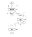
まず、ステップS100において、光源駆動回路16の電源がONされる。 First, in step S100, the light
次のステップS101において、電流値規定部32は、温度センサ34によって、環境温度を測定、把握する。 In the next step S <b> 101, the current
そして、ステップS102において、電流値規定部32は、環境温度が所定の値、例えば0℃以上であるか否かを判別する。 In step S102, the current
環境温度が所定の値よりも低い、すなわち0℃以上ではないとき(S102においてNoの場合)、ステップS103において電流値規定部32は、LED8の駆動電流値を所定電流値よりも低い値である補正電流値、例えば20mAと設定する。図6(b)に示すように、環境温度Tが0℃以下の場合である例えば−25℃の場合には、駆動電流が20mAの時のLEDのVf値は、3.6Vである(E点)。 When the environmental temperature is lower than a predetermined value, that is, not higher than 0 ° C. (in the case of No in S102), in Step S103, the current
次に、図7におけるステップS104では、電流値規定部32は所定時間待機する。この待機時間は、LEDの動作開始時からの温度上昇に応じて適宜定められるものであり、10秒から数十秒程度の時間である。なお、この待機時間が短すぎると、電流値規定部32での処理が多発する一方、待機時間が長すぎると、後述するLEDのVfが一定の電圧値以下に下がった場合の動作が遅れ、低電流であるための発光輝度が低い状態で長時間LEDを点灯させることになり、高輝度の画像表示を行う観点からは好ましくない。また、この待機時間の設定は、必要に応じて行われればよく、必須のものではない。 Next, in step S104 in FIG. 7, the current
次のステップS105で、電流値規定部32は、再び温度センサ34によって環境温度を把握し、所定の温度である0℃以上であるか否かを判別する。以下、環境温度が所定の温度である0度以上になるまで、このステップS104とS105が繰り返される。 In the next step S105, the current
環境温度が0度以上となった場合、すなわちステップS105でYesとなった場合には、ステップS106で、電流値規定部32はLEDの駆動電流値を所定電流値である、例えば30mAとする。 When the environmental temperature is 0 ° C. or higher, that is, when the answer is Yes in Step S105, the current
図6(b)に示すように、環境温度が0℃の場合には、補正電流値である駆動電流値Iが20mAの場合にはVf=3.3Vであるが(A’点)、駆動電流値Iが所定電流値である30mAの場合にはVf=3.6Vとなる(A点)。 As shown in FIG. 6B, when the environmental temperature is 0 ° C., when the drive current value I, which is a correction current value, is 20 mA, Vf = 3.3 V (point A ′). When the current value I is 30 mA, which is a predetermined current value, Vf = 3.6 V (point A).
以下、図7に示すように、バックライトがOFFされるステップS107まで、ステップS106の環境温度が安定している場合の、所定電流値による駆動が行われる。 Hereinafter, as shown in FIG. 7, until the step S107 when the backlight is turned off, the driving with the predetermined current value is performed when the environmental temperature in the step S106 is stable.
なお、ステップS102で、環境温度が所定の値である0℃以上である場合、すなわちYesの場合には、電流値規定部32は、そのまま所定電流値での駆動を行うためにLEDの駆動電流値を所定電流値である30mAとする。 In step S102, when the environmental temperature is equal to or higher than a predetermined value of 0 ° C., that is, in the case of Yes, the current
図6(b)に示すように、環境温度Tが0℃以上の場合には、環境温度が25℃の場合にVf=3.3V(B点)、環境温度が50℃の場合はVf=3.0Vと、環境温度が高くなるほどVfの値が小さくなる。この結果、本実施形態の光源駆動回路においてVinの値を設計する場合には、LEDのVf値の最大値である3.6Vとトランジスタ39の動作マージン電圧である0.6Vを加えた4.2Vとすることができる。一方、環境温度が0℃以下の場合にも所定電流値である30mAを動作電流値とすると、Vinの値を設計するにおいては、最大のVf値である3.9Vと、トランジスタ39の動作マージン電圧である0.6Vを加えた4.5V以上としなくてはならないから、本実施形態の光源駆動回路16では回路効率の低下を有効に防止できていることが分かる。 As shown in FIG. 6B, when the environmental temperature T is 0 ° C. or higher, Vf = 3.3 V (point B) when the environmental temperature is 25 ° C., and Vf = 3 when the environmental temperature is 50 ° C. The value of Vf decreases as the environmental temperature increases to 3.0V. As a result, when designing the value of Vin in the light source driving circuit of this embodiment, the maximum value of Vf value of the LED is 3.6V and the operating margin voltage of the
なお、補正電流値として所定電流値よりも低い電流値でLEDを駆動させた場合には、図4(a)に示したとおりLEDからの発光輝度は低くなる。しかし、LED自体が動作することによって発熱するために、補正電流値でLEDを駆動する時間自体が限られている。また、図7のフローチャートで示したように、補正電流値でLEDを駆動するのはバックライトの動作開始からの一定時間に限られるために、表示装置の表示画像を見ている監視者が大きな違和感を持つことは少ない。特に、補正電流値での動作を行うか否かの判断基準となる、所定の環境温度の値を適切に定めることにより、補正動作を行う場合が冬季の早朝など限られた期間に限定されるために、実用上の問題が生じることは無いと判断することができる。 When the LED is driven with a current value lower than the predetermined current value as the correction current value, the light emission luminance from the LED becomes low as shown in FIG. However, because the LED itself generates heat, the time itself for driving the LED with the correction current value is limited. Further, as shown in the flowchart of FIG. 7, since the LED is driven with the correction current value only for a certain time from the start of the operation of the backlight, a large number of observers are viewing the display image on the display device. There are few uncomfortable feelings. In particular, by appropriately setting a predetermined environmental temperature value, which is a criterion for determining whether or not to perform the operation with the corrected current value, the case where the correcting operation is performed is limited to a limited period such as early morning in winter. Therefore, it can be determined that no practical problem occurs.
図8は、本実施形態の光源駆動回路でのLEDの動作を示すために、LEDの各種特性値の時間変化をグラフとして表したものである。なお、本実施形態の光源駆動回路としては、補正電流値を1つに限定する必要はなく、より滑らかな補正電流値でのLEDの駆動を行い、かつ、動作マージンをより低減した高い動作効率の光源駆動回路を得るためには、補正電流値として最も小さい動作電流値の第1の補正電流値と、第1の補正電流値よりは大きく所定電流値よりも小さい第2の補正電流の2段階とすることもできる。このため、図8ではこのような、電流値規定部が、環境温度の所定値として、第1の所定値と第2の所定値に基づいて、第1の補正電流値と第2の補正電流値を用いて、動作電流値の補正を行った状況について説明する。 FIG. 8 is a graph showing changes over time in various characteristic values of the LED in order to show the operation of the LED in the light source driving circuit of the present embodiment. Note that the light source driving circuit of the present embodiment does not have to limit the correction current value to one, and the LED is driven with a smoother correction current value, and the operation margin is further reduced and the operation efficiency is reduced. In order to obtain the light source driving circuit, the first correction current value having the smallest operation current value as the correction current value and the second correction current 2 which is larger than the first correction current value and smaller than the predetermined current value. It can also be a stage. For this reason, in FIG. 8, such a current value defining unit uses the first correction current value and the second correction current as the predetermined value of the environmental temperature based on the first predetermined value and the second predetermined value. A situation in which the operating current value is corrected using the value will be described.
図8(a)は、LEDの駆動電流値の時間変化を示している。なお、本実施形態の光源駆動回路では、PWM制御を行っているため、LEDの電流値は間欠的なものとして示されている。 FIG. 8A shows the change over time in the LED drive current value. In the light source driving circuit of the present embodiment, since the PWM control is performed, the current value of the LED is shown as intermittent.
図8(a)に示すように、バックライトの動作開始時であるt0時点では、環境温度は第1の所定値よりも低く、電流値規定部によって、LEDの駆動電流値は最も小さい第1の補正電流値I1とされている。そして、一定の時間が経過した時間t1において、LEDの動作に伴って環境温度が高くなり、第1の所定値よりも高くなったことから、電流値規定部は、LEDの駆動電流値を第2の補正電流値I2とする。さらに、時間が経過した時間t2において、環境温度はさらに高くなって第2の所定よりも高くなったことから、電流値規定部が駆動電流値を所定電流値I3とする。As shown in FIG. 8A, at the time t0 when the backlight operation starts, the environmental temperature is lower than the first predetermined value, and the current value defining unit causes the LED driving current value to be the smallest. The correction current value I1 is1 . Then, at time t1 when a certain time has elapsed, the ambient temperature has increased with the operation of the LED and has become higher than the first predetermined value, so that the current value defining unit determines the drive current value of the LED. The second correction current value is I2 . Furthermore, in the time t2 elapsed time, since the environmental temperature is higher than the second predetermined even higher, the current value defining portion is a predetermined current value I3 the drive current value.
図8(b)は、LEDの端子間電圧値Vfの変化を実線42として示す。まず動作開始時のt0では、第1の補正電流値I1が流れた場合の第1の所定値よりも低い環境温度におけるLEDの端子間電圧値V1である。時間が経過するにつれて、環境温度が徐々に高くなるため、LEDの端子間電圧値は徐々に小さい値になる。時間t1において、LEDの駆動電流値が第2の補正電流値I2となったことに伴い、端子間電圧値は、環境温度が第1の所定値である場合における第2の補正電流値が流れた場合の端子間電圧値V2となる。環境温度はさらに上昇するため、端子間電圧値は再び徐々に低下する。時間t2において、環境温度が第2の所定値となったため、所定電流値での駆動状態に移行する。このときの端子間電圧値は、環境温度が第2の所定値である場合における所定電流値が流れた場合のV3となる。FIG. 8B shows a change in the inter-terminal voltage value Vf of the LED as a
図8(b)に示すように、本実施形態の光源駆動回路では、環境温度の変化に関わりなく、LEDの端子間電圧値Vfを時間t2における値であるV3より小さい値に保つことができる。従って、光源駆動回路に用いられる電源の電圧値を設計する場合において、Vfの値を図8(b)に一点鎖線45で示すV3の値として設計することができる。図8(b)には、比較として駆動電流値を常に所定電流値とした場合も点線43で示す。この場合には、動作開始時であるt0では、LEDの端子間電圧はV4となるため、光源駆動回路において電圧源の電圧値を設定するに際して、例えば二点鎖線44で示すV5の値としなくてはならない。このことは、上記したように、環境温度が低い特殊な状態における動作マージンを確保するために、光源駆動回路の電圧源の電圧値を高くすることになるため、所定電流値での動作時の回路効率の低下を回避することはできない。As shown in FIG. 8B, in the light source driving circuit of this embodiment, the voltage value Vf between the terminals of the LED is kept at a value smaller than V3 that is the value at time t2 regardless of the change in the environmental temperature. Can do. Therefore, when designing the voltage value of the power source used in the light source driving circuit, the value of Vf can be designed as the value of V3 indicated by the alternate long and
図8(c)は、LEDの温度の変化を示す。LEDの温度は、動作開示時であるt0では環境温度と同じ値を示すが、LED自体の動作に伴う発熱により、時間経過と共に徐々に高くなっている。FIG. 8C shows a change in the temperature of the LED. The temperature of the LED shows the same value as the ambient temperature at t0 when the operation is disclosed, but gradually increases with time due to heat generated by the operation of the LED itself.
図8(d)は、LEDからの発光輝度の変化を示している。駆動電流値と環境温度の変化により、LEDからの発光輝度は、時間t0での輝度B1から一旦減少し、時間t1でB2となり、さらに時間の経過とともに減少して、時間t2においてB3となる。以後は、環境温度の変化は乏しくなるため、所定電流値で駆動された場合の輝度B3を保つこととなる。FIG. 8D shows a change in the light emission luminance from the LED. Due to changes in the drive current value and the environmental temperature, the light emission luminance from the LED once decreases from the luminance B1 at time t0 , becomes B2 at time t1 , and further decreases with time, and decreases to time t2. the B3 in. Thereafter, since the change in the environmental temperature becomes scarce, the luminance B3 when driven at a predetermined current value is maintained.
図8(d)に、補正電流値での駆動を行わない場合のLEDの輝度を点線48で示す。図8(d)から明らかなように、動作開始時のt0において、本実施形態の光源駆動回路の場合のLEDからの発光輝度B1は、電流値補正を行わない場合の輝度B4と比較すると低い値となっている。しかし上記したように、補正電流値で駆動する場合自体が冬季の早朝など環境温度が特に低い稀な場合であり、また、図8(d)から明らかなように、輝度が低い状態は、動作開始時のt0からt2の期間に限られる。このt0からt2の時間は、長くても数分から数十分程度であるため、バックライトとしての動作における実用上の影響は考慮しなくてもよい。In FIG. 8D, the dotted
なお、上記、本実施形態にかかるバックライトについて、補正電流値での光源駆動状態から所定電流値での駆動状態に移行する条件を、環境温度を温度センサによって実際に測定し、その値が所定の温度よりも高くなった場合として説明した。しかし、上述のとおり、環境温度の変化は主としてLEDが動作することによる発熱で生じるため、環境温度の上昇を一定以上の精度で、あらかじめ予測することも可能である。この場合には、所定電流値での光源駆動状態への移行を、環境温度の測定によってではなく、補正動作開始時からの経過時間によって定めることも可能である。 In the above-described backlight according to the present embodiment, the environmental temperature is actually measured by the temperature sensor under the condition for shifting from the light source driving state at the correction current value to the driving state at the predetermined current value, and the value is predetermined. It has been described as a case where the temperature is higher than the temperature of. However, as described above, the change in the environmental temperature is mainly caused by heat generated by the operation of the LED. Therefore, the increase in the environmental temperature can be predicted in advance with a certain degree of accuracy. In this case, the transition to the light source driving state at a predetermined current value can be determined not by measuring the environmental temperature but by the elapsed time from the start of the correction operation.
また、本実施形態では、液晶表示装置のバックライトとして、アクティブバックライト方式のものとして用いることを説明したが、本発明はこれに限られるものではない。アクティブバッライト方式ではない、常に一定輝度の面状の照射光を照射する照明装置においても、光源の電気的特性値が所定の温度特性を有している場合には、光源駆動回路の効率低下を有効に防止することができるという効果を得ることができることは、言うまでもない。 In the present embodiment, the active backlight system is used as the backlight of the liquid crystal display device, but the present invention is not limited to this. Even in an illuminating device that irradiates planar illumination light with a constant luminance, which is not an active backlight method, the efficiency of the light source drive circuit decreases when the electrical characteristic value of the light source has a predetermined temperature characteristic. Needless to say, it is possible to obtain an effect that can be effectively prevented.
さらに、上記本実施形態においては、光源に含まれる発光素子としてLEDを用いる場合を示したが、本発明はこれに限られるものではなく、EL光源など、電気的特性値が環境温度によって変化する他の発光素子を光源に用いることができる。 Furthermore, in the present embodiment, the case where an LED is used as the light emitting element included in the light source has been described. However, the present invention is not limited to this, and an electrical characteristic value such as an EL light source varies depending on the environmental temperature. Other light emitting elements can be used as the light source.
また、本発明にかかる照明装置の用途として液晶表示装置のバックライトとして用いる例を示したが、本発明にかかる照明装置は、効率よく所定の輝度の照射光を照射することができ、しかも部分部分の照射光の色や輝度を変化させることができる薄型の照明装置であるため、天井や壁面に埋め込まれる光源や、ショーケースなどに用いられる照明装置として幅広い用途を有するものである。 Moreover, although the example used as a backlight of a liquid crystal display device was shown as an application of the illumination device according to the present invention, the illumination device according to the present invention can efficiently irradiate irradiation light with a predetermined luminance, and further Since it is a thin illuminating device that can change the color and brightness of the irradiation light of a part, it has a wide range of uses as a illuminating device used for a light source embedded in a ceiling or a wall surface, a showcase or the like.
本発明は、環境温度によりその電気的特性値が変化する発光素子を用いた場合に、光源駆動回路の効率低下を効果的に防止することができる照明装置として、また、この照明装置を表示部のバックライトとして用いた表示装置として産業上利用可能である。 The present invention provides a lighting device capable of effectively preventing a reduction in the efficiency of a light source driving circuit when a light emitting element whose electrical characteristic value changes depending on an environmental temperature is used. It can be used industrially as a display device used as a backlight.
1 液晶表示装置
2 液晶パネル
3、4 透明基板
5、6 偏光板
7 バックライト
8 発光素子(LED)
9 シャーシ
16 光源駆動回路
31 定電圧電源(Vin)
32 電流値規定部
32 電流値制御部
39 電流値制御素子(トランジスタ)DESCRIPTION OF
9
32 Current
Claims (8)
Translated fromJapanese前記光源駆動回路は、
前記発光素子に供給される前記駆動電流の電流値を定める電流値規定部と、
前記駆動電流を供給するための定電圧電源と、
前記発光素子に前記電流値規定部で定められた電流値の駆動電流が流れるように制御する電流値制限部と、
環境温度を測定する温度センサとを有し、
前記定電圧電源に、前記発光素子と前記電流値制限部とが直列に接続され、
前記温度センサで検出された環境温度が所定温度よりも低い場合に、前記電流値規定部は、前記駆動電流の電流値を所定電流値よりも小さい値の補正電流値と定めることを特徴とする照明装置。A light source including a light emitting element whose electrical characteristic value varies depending on an ambient temperature; and a light source driving circuit that supplies a driving current to the light emitting element to emit light, and isdisplayed on the display unit of the display device by the display unit. An illumination device that emits irradiation light corresponding to an image,
The light source driving circuit includes:
A current value defining part for defining a current value of the drive current supplied to the light emitting element;
A constant voltage power supply for supplying the drive current;
A current value limiting unit for controlling the driving current of the current value determined by the current value defining unit to flow through the light emitting element;
A temperature sensor for measuring the environmental temperature,
The light emitting element and the current value limiting unit are connected in series to the constant voltage power source,
When the environmental temperature detected by the temperature sensor is lower than a predetermined temperature, the current value defining unit determines the current value of the driving current as a corrected current value that is smaller than the predetermined current value. Lighting device.
Priority Applications (1)
| Application Number | Priority Date | Filing Date | Title |
|---|---|---|---|
| JP2008020527AJP5247172B2 (en) | 2008-01-31 | 2008-01-31 | LIGHTING DEVICE AND DISPLAY DEVICE HAVING THE SAME |
Applications Claiming Priority (1)
| Application Number | Priority Date | Filing Date | Title |
|---|---|---|---|
| JP2008020527AJP5247172B2 (en) | 2008-01-31 | 2008-01-31 | LIGHTING DEVICE AND DISPLAY DEVICE HAVING THE SAME |
Publications (2)
| Publication Number | Publication Date |
|---|---|
| JP2009181839A JP2009181839A (en) | 2009-08-13 |
| JP5247172B2true JP5247172B2 (en) | 2013-07-24 |
Family
ID=41035640
Family Applications (1)
| Application Number | Title | Priority Date | Filing Date |
|---|---|---|---|
| JP2008020527AExpired - Fee RelatedJP5247172B2 (en) | 2008-01-31 | 2008-01-31 | LIGHTING DEVICE AND DISPLAY DEVICE HAVING THE SAME |
Country Status (1)
| Country | Link |
|---|---|
| JP (1) | JP5247172B2 (en) |
Cited By (1)
| Publication number | Priority date | Publication date | Assignee | Title |
|---|---|---|---|---|
| US10504406B2 (en) | 2017-04-11 | 2019-12-10 | Samsung Electronics Co., Ltd. | Pixel circuit of display panel and display device |
Families Citing this family (4)
| Publication number | Priority date | Publication date | Assignee | Title |
|---|---|---|---|---|
| KR101005566B1 (en) | 2010-10-08 | 2011-01-05 | (주)레프코리아 | Luminaire with temperature control and heat dissipation |
| EP2742776B1 (en) | 2011-08-08 | 2021-05-26 | Quarkstar LLC | Dimmable lighting devices and methods for dimming same |
| CN113189831B (en)* | 2020-01-14 | 2023-04-25 | 青岛海信激光显示股份有限公司 | Laser projection apparatus and driving method thereof |
| WO2025009367A1 (en)* | 2023-07-06 | 2025-01-09 | ソニーグループ株式会社 | Control device, control method, and video device |
Family Cites Families (5)
| Publication number | Priority date | Publication date | Assignee | Title |
|---|---|---|---|---|
| JPH04100748A (en)* | 1990-08-14 | 1992-04-02 | Stanley Electric Co Ltd | LED lamp for vehicle |
| JPH11298044A (en)* | 1998-04-16 | 1999-10-29 | Sony Corp | Light source drive circuit |
| JP2004330819A (en)* | 2003-05-01 | 2004-11-25 | Koito Mfg Co Ltd | Lighting fixture for vehicle |
| JP2007147870A (en)* | 2005-11-25 | 2007-06-14 | Sharp Corp | Display device |
| JP4869744B2 (en)* | 2006-03-09 | 2012-02-08 | 株式会社 日立ディスプレイズ | LED lighting device and liquid crystal display device using the same |
- 2008
- 2008-01-31JPJP2008020527Apatent/JP5247172B2/ennot_activeExpired - Fee Related
Cited By (1)
| Publication number | Priority date | Publication date | Assignee | Title |
|---|---|---|---|---|
| US10504406B2 (en) | 2017-04-11 | 2019-12-10 | Samsung Electronics Co., Ltd. | Pixel circuit of display panel and display device |
Also Published As
| Publication number | Publication date |
|---|---|
| JP2009181839A (en) | 2009-08-13 |
Similar Documents
| Publication | Publication Date | Title |
|---|---|---|
| EP2328139B1 (en) | Method of controlling power consumption of a backlight device, a backlight device for an image display device, display device, and a television reception device | |
| US7312783B2 (en) | Light emitting element drive device and display apparatus | |
| JP5070331B2 (en) | LIGHTING DEVICE AND DISPLAY DEVICE HAVING THE SAME | |
| JP5542303B2 (en) | Light source system and display device | |
| TWI393100B (en) | Display device and driving method thereof | |
| US8207933B2 (en) | Backlight unit, liquid crystal display device including the same, and method of driving liquid crystal display device | |
| JP4720757B2 (en) | Light source device and liquid crystal display device | |
| JP4915143B2 (en) | Display device and driving method thereof | |
| WO2010016440A1 (en) | Backlight and display device using the same | |
| JP4734900B2 (en) | Backlight device | |
| JP2009163945A (en) | Light source system and display | |
| JP4882657B2 (en) | Backlight control device, backlight control method, and liquid crystal display device | |
| JP2007123279A (en) | Driving device for backlight, backlight assembly, liquid crystal display device having the same, and driving method for backlight | |
| US20090051637A1 (en) | Display devices | |
| US8305332B2 (en) | Backlight unit, liquid crystal display device including the same, and localized dimming method thereof | |
| JP2010078802A (en) | Liquid crystal display | |
| US20110285313A1 (en) | Light-emitting element driving device and display device | |
| JP5247172B2 (en) | LIGHTING DEVICE AND DISPLAY DEVICE HAVING THE SAME | |
| KR101021202B1 (en) | FCS mode liquid crystal display device having low temperature compensation circuit and its driving method | |
| JP4995120B2 (en) | LIGHTING DEVICE AND DISPLAY DEVICE HAVING THE SAME | |
| JP2006145886A (en) | Display device and its control method | |
| JP2009157190A (en) | Light source system, light source control device, light source device, and image display method | |
| US20080001879A1 (en) | Driving method of liquid crystal display device | |
| KR101511128B1 (en) | Method for driving light emitting diode, back light assembly for performing the method and display apparatus having the back light assembly | |
| KR100752848B1 (en) | Inverter drive control method of LCD |
Legal Events
| Date | Code | Title | Description |
|---|---|---|---|
| A621 | Written request for application examination | Free format text:JAPANESE INTERMEDIATE CODE: A621 Effective date:20100302 | |
| A977 | Report on retrieval | Free format text:JAPANESE INTERMEDIATE CODE: A971007 Effective date:20111128 | |
| A131 | Notification of reasons for refusal | Free format text:JAPANESE INTERMEDIATE CODE: A131 Effective date:20111220 | |
| A521 | Request for written amendment filed | Free format text:JAPANESE INTERMEDIATE CODE: A523 Effective date:20120217 | |
| A131 | Notification of reasons for refusal | Free format text:JAPANESE INTERMEDIATE CODE: A131 Effective date:20120712 | |
| A521 | Request for written amendment filed | Free format text:JAPANESE INTERMEDIATE CODE: A523 Effective date:20120907 | |
| TRDD | Decision of grant or rejection written | ||
| A01 | Written decision to grant a patent or to grant a registration (utility model) | Free format text:JAPANESE INTERMEDIATE CODE: A01 Effective date:20130314 | |
| A61 | First payment of annual fees (during grant procedure) | Free format text:JAPANESE INTERMEDIATE CODE: A61 Effective date:20130409 | |
| R150 | Certificate of patent or registration of utility model | Free format text:JAPANESE INTERMEDIATE CODE: R150 | |
| FPAY | Renewal fee payment (event date is renewal date of database) | Free format text:PAYMENT UNTIL: 20160419 Year of fee payment:3 | |
| LAPS | Cancellation because of no payment of annual fees |