JP5245614B2 - Light emitting device - Google Patents
Light emitting deviceDownload PDFInfo
- Publication number
- JP5245614B2 JP5245614B2JP2008194903AJP2008194903AJP5245614B2JP 5245614 B2JP5245614 B2JP 5245614B2JP 2008194903 AJP2008194903 AJP 2008194903AJP 2008194903 AJP2008194903 AJP 2008194903AJP 5245614 B2JP5245614 B2JP 5245614B2
- Authority
- JP
- Japan
- Prior art keywords
- filler
- sealing material
- light emitting
- emitting device
- light
- Prior art date
- Legal status (The legal status is an assumption and is not a legal conclusion. Google has not performed a legal analysis and makes no representation as to the accuracy of the status listed.)
- Expired - Fee Related
Links
Images


Classifications
- H—ELECTRICITY
- H10—SEMICONDUCTOR DEVICES; ELECTRIC SOLID-STATE DEVICES NOT OTHERWISE PROVIDED FOR
- H10H—INORGANIC LIGHT-EMITTING SEMICONDUCTOR DEVICES HAVING POTENTIAL BARRIERS
- H10H20/00—Individual inorganic light-emitting semiconductor devices having potential barriers, e.g. light-emitting diodes [LED]
- H10H20/80—Constructional details
- H10H20/85—Packages
- H10H20/852—Encapsulations
- H10H20/854—Encapsulations characterised by their material, e.g. epoxy or silicone resins
- H—ELECTRICITY
- H01—ELECTRIC ELEMENTS
- H01L—SEMICONDUCTOR DEVICES NOT COVERED BY CLASS H10
- H01L2224/00—Indexing scheme for arrangements for connecting or disconnecting semiconductor or solid-state bodies and methods related thereto as covered by H01L24/00
- H01L2224/01—Means for bonding being attached to, or being formed on, the surface to be connected, e.g. chip-to-package, die-attach, "first-level" interconnects; Manufacturing methods related thereto
- H01L2224/02—Bonding areas; Manufacturing methods related thereto
- H01L2224/04—Structure, shape, material or disposition of the bonding areas prior to the connecting process
- H01L2224/04042—Bonding areas specifically adapted for wire connectors, e.g. wirebond pads
- H—ELECTRICITY
- H01—ELECTRIC ELEMENTS
- H01L—SEMICONDUCTOR DEVICES NOT COVERED BY CLASS H10
- H01L2224/00—Indexing scheme for arrangements for connecting or disconnecting semiconductor or solid-state bodies and methods related thereto as covered by H01L24/00
- H01L2224/01—Means for bonding being attached to, or being formed on, the surface to be connected, e.g. chip-to-package, die-attach, "first-level" interconnects; Manufacturing methods related thereto
- H01L2224/10—Bump connectors; Manufacturing methods related thereto
- H01L2224/15—Structure, shape, material or disposition of the bump connectors after the connecting process
- H01L2224/16—Structure, shape, material or disposition of the bump connectors after the connecting process of an individual bump connector
- H01L2224/161—Disposition
- H01L2224/16151—Disposition the bump connector connecting between a semiconductor or solid-state body and an item not being a semiconductor or solid-state body, e.g. chip-to-substrate, chip-to-passive
- H01L2224/16221—Disposition the bump connector connecting between a semiconductor or solid-state body and an item not being a semiconductor or solid-state body, e.g. chip-to-substrate, chip-to-passive the body and the item being stacked
- H01L2224/16245—Disposition the bump connector connecting between a semiconductor or solid-state body and an item not being a semiconductor or solid-state body, e.g. chip-to-substrate, chip-to-passive the body and the item being stacked the item being metallic
- H—ELECTRICITY
- H01—ELECTRIC ELEMENTS
- H01L—SEMICONDUCTOR DEVICES NOT COVERED BY CLASS H10
- H01L2224/00—Indexing scheme for arrangements for connecting or disconnecting semiconductor or solid-state bodies and methods related thereto as covered by H01L24/00
- H01L2224/01—Means for bonding being attached to, or being formed on, the surface to be connected, e.g. chip-to-package, die-attach, "first-level" interconnects; Manufacturing methods related thereto
- H01L2224/42—Wire connectors; Manufacturing methods related thereto
- H01L2224/47—Structure, shape, material or disposition of the wire connectors after the connecting process
- H01L2224/48—Structure, shape, material or disposition of the wire connectors after the connecting process of an individual wire connector
- H01L2224/4805—Shape
- H01L2224/4809—Loop shape
- H01L2224/48091—Arched
- H—ELECTRICITY
- H01—ELECTRIC ELEMENTS
- H01L—SEMICONDUCTOR DEVICES NOT COVERED BY CLASS H10
- H01L2224/00—Indexing scheme for arrangements for connecting or disconnecting semiconductor or solid-state bodies and methods related thereto as covered by H01L24/00
- H01L2224/01—Means for bonding being attached to, or being formed on, the surface to be connected, e.g. chip-to-package, die-attach, "first-level" interconnects; Manufacturing methods related thereto
- H01L2224/42—Wire connectors; Manufacturing methods related thereto
- H01L2224/47—Structure, shape, material or disposition of the wire connectors after the connecting process
- H01L2224/49—Structure, shape, material or disposition of the wire connectors after the connecting process of a plurality of wire connectors
- H01L2224/491—Disposition
- H01L2224/49105—Connecting at different heights
- H01L2224/49107—Connecting at different heights on the semiconductor or solid-state body
- H—ELECTRICITY
- H01—ELECTRIC ELEMENTS
- H01L—SEMICONDUCTOR DEVICES NOT COVERED BY CLASS H10
- H01L2224/00—Indexing scheme for arrangements for connecting or disconnecting semiconductor or solid-state bodies and methods related thereto as covered by H01L24/00
- H01L2224/73—Means for bonding being of different types provided for in two or more of groups H01L2224/10, H01L2224/18, H01L2224/26, H01L2224/34, H01L2224/42, H01L2224/50, H01L2224/63, H01L2224/71
- H01L2224/732—Location after the connecting process
- H01L2224/73201—Location after the connecting process on the same surface
- H01L2224/73203—Bump and layer connectors
- H01L2224/73204—Bump and layer connectors the bump connector being embedded into the layer connector
- H—ELECTRICITY
- H01—ELECTRIC ELEMENTS
- H01L—SEMICONDUCTOR DEVICES NOT COVERED BY CLASS H10
- H01L2224/00—Indexing scheme for arrangements for connecting or disconnecting semiconductor or solid-state bodies and methods related thereto as covered by H01L24/00
- H01L2224/73—Means for bonding being of different types provided for in two or more of groups H01L2224/10, H01L2224/18, H01L2224/26, H01L2224/34, H01L2224/42, H01L2224/50, H01L2224/63, H01L2224/71
- H01L2224/732—Location after the connecting process
- H01L2224/73251—Location after the connecting process on different surfaces
- H01L2224/73265—Layer and wire connectors
- H—ELECTRICITY
- H10—SEMICONDUCTOR DEVICES; ELECTRIC SOLID-STATE DEVICES NOT OTHERWISE PROVIDED FOR
- H10H—INORGANIC LIGHT-EMITTING SEMICONDUCTOR DEVICES HAVING POTENTIAL BARRIERS
- H10H20/00—Individual inorganic light-emitting semiconductor devices having potential barriers, e.g. light-emitting diodes [LED]
- H10H20/80—Constructional details
- H10H20/882—Scattering means
Landscapes
- Led Device Packages (AREA)
Description
Translated fromJapanese本発明は、発光素子が封止材により封止される発光装置に関する。 The present invention relates to a light emitting device in which a light emitting element is sealed with a sealing material.
従来、1次光を放出する発光素子と、発光素子を覆うように設けられJISA値で50以上の硬度を有するシリコーンと、シリコーンに含有され、1次光を吸収して可視光を放出する蛍光体と、を備えたことを特徴とする発光装置が提案されている(特許文献1参照)。そして、このようなシリコーンを封止体として用いることにより、耐光性、耐候性、機械的耐久性に優れた波長変換型の発光装置を実現することができるとされている。
しかし、特許文献1に記載の発光装置では、硬度の比較的高い封止樹脂を用いているため、例えばワイヤー等の電気的接続部位に加わる応力が比較的大きいものとなる。電気的接続部位に加わる応力が大きいと、過酷な条件で使用した際に断線が生じるおそれがあり、電気的接続部位に加わる応力は小さい方がのぞましい。 However, since the light emitting device described in
本発明は、前記事情に鑑みてなされたものであり、その目的とするところは、硬度の比較的低い封止樹脂を用いても、発光素子の封止部分の強度を確保することのできる発光装置を提供することにある。 The present invention has been made in view of the above circumstances, and an object of the present invention is to emit light that can ensure the strength of a sealing portion of a light emitting element even when a sealing resin having a relatively low hardness is used. To provide an apparatus.
前記目的を達成するため、本発明では、青色光を発する発光素子と、前記発光素子を封止するショア硬度Aが60以下の封止材と、前記封止材に10〜20重量%の割合で含有される第1フィラーと、前記封止材に5〜20重量%の割合で含有され、前記第1フィラーよりも粒径の小さな第2フィラーと、を備え、前記第1フィラーは、平均粒径(d50)が10〜30μmであり、前記第2フィラーは、平均粒径(d50)が0.1〜1.0μmであり、前記第1フィラー及び前記第2フィラーは、前記封止材の強度向上に寄与し、前記第2フィラーは、前記封止材のガスバリア性を向上させる発光装置が提供される。In order to achieve the object, in the present invention, a light emitting element emitting blue light,a sealing material having aShore hardness A of 60 or less for sealing the light emitting element, anda ratio of10 to20% by weight in the sealing materialin a first filler contained, the are containedin a proportion of the sealing material5 to 20 wt%, and a small second filler particle size than the first filler, said first filler has an average The particle size (d50 ) is 10 to 30 μm, the second filler has an average particle size (d50 ) of 0.1 to 1.0 μm, and the first filler and the second filler are sealed A light emitting device is provided that contributes to improving the strength of the stopper and the second filler improves the gas barrier properties of the sealing material.
上記発光装置において、前記第1フィラーと前記第2フィラーに加えて5〜20重量%の割合で第3フィラーを封止材に含有させても良い。この第3フィラーは、平均粒径(d50)が0.01〜0.04μmであってガスバリア性と粘度を向上させる。この第3フィラーは増粘剤であってもよい。In the light emitting device, in addition to the first filler and the second filler, a third filler may be included in the sealing materialat a ratio of 5 to20% by weight . This third filler has an average particle size (d50 ) of 0.01 to 0.04 μm and improves gas barrier properties and viscosity. This third filler may be a thickener.
上記発光装置において、前記第1フィラーは、蛍光体であってもよい。 In the light emitting device, the first filler may be a phosphor.
上記発光装置において、前記第2フィラーは、SiO2からなり、前記封止材は、シリコーンからなっていてもよい。In the above light emitting device, the second filler may be made of SiO2 , and the sealing material may be made of silicone.
上記発光装置において、前記第1フィラーの平均粒径は、前記発光素子のピーク波長よりも大きく、前記第2フィラーの平均粒径は、前記発光素子のピーク波長よりも小さいことが好ましい。 In the above light emitting device, it is preferable that an average particle diameter of the first filler is larger than a peak wavelength of the light emitting element, and an average particle diameter of the second filler is smaller than a peak wavelength of the light emitting element.
本発明によれば、硬度の比較的低い封止樹脂を用いても、発光素子の封止部分の強度を確保することができる。 According to the present invention, the strength of the sealing portion of the light emitting element can be ensured even when a sealing resin having a relatively low hardness is used.
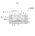
図1及び図2は本発明の一実施形態を示し、図1は発光装置の平面図、図2は発光装置の断面図である。 1 and 2 show an embodiment of the present invention, FIG. 1 is a plan view of a light emitting device, and FIG. 2 is a cross-sectional view of the light emitting device.
図1に示すように、この発光装置1は、発光素子としてのLEDチップ11と、LEDチップ11を包囲するリフレクタ部12aを含んで形成される凹部13を有する樹脂製のケース12と、ケース12の凹部13の底面に露出し互いに左右方向について離隔して配置された金属製の第1リード14及び第2リード15と、凹部13内に充填される樹脂製の封止材16と、を備えている。また、発光装置1は、LEDチップ11の一方の電極11aと第1リード14とを接続する第1ワイヤ17と、LEDチップ11の他方の電極11bと第2リード15とを接続する第2ワイヤ18と、保護素子としてのツェナーダイオード19と、ツェナーダイオード19の上面に形成された電極19aと第1リード14とを接続する第3ワイヤ20と、を備えている。各ワイヤ17,18,20は、金により構成されている。 As shown in FIG. 1, the
ケース12は、全体として略直方体状を呈し、各リード14,15が凹部13の底面の一部をなすとともに、ケース12の樹脂が凹部13の底面の他部をなしている。各リード14,15は、ケース11の外側まで延び、図示しない外部接続端子と電気的に接続される。ケース12は、例えば、液晶ポリマ(LCP)、ポリフェニレンサルファイド(PPS)、シンジオタクチックポリスチレン(SPS)、ポリフタルアミド(PPA)、ナイロン等の熱可塑性樹脂からなり、各リード14,15とケース12とはトランスファモールド、インジェクション等の成形法により成形されている。 The
凹部13の開口部は、上面視にて円形状を呈している。リフレクタ部12aの内周面は、上方へ向かって拡がるよう形成されている。凹部13の内部はLEDチップ11、ツェナーダイオード19及び各ワイヤ17,18,20を封止する透光性の封止材16で満たされており、凹部13からLEDチップ11の光が取り出される。 The opening of the
LEDチップ11は、上面側に一対の電極11a,11bが形成されるフェイスアップ型である。本実施形態においては、LEDチップ11として、GaN系半導体を含み青色光を発するものが用いられる。LEDチップ11は、エポキシ系のダイボンドペースト11c(図2参照)により第1リード14に固定されている。 The
第1リード14と第2リード15は、銀メッキが施された導電性の金属からなる。第1リード14及び第2リード15は、所定の厚さ寸法及び幅寸法で形成されており、長手方向端部がケース12の凹部13内に位置している。凹部13内における第1リード14及び第2リード15の端部は、互いに離隔するよう凹部13の底面に配置される。 The
図2は、発光装置の断面図である。
図2に示すように、封止材16は、凹部13内に充填され、LEDチップ11、ツェナーダイオード19及び各ワイヤ17,18,20を封止している。本実施形態においては、封止材16は、エポキシ系の樹脂に比して、熱、光等による黄変が生じ難いエラストマ型のシリコーン系の樹脂からなる。封止材16は、各ワイヤ17,18,20への応力を考慮すると、ショア硬度Aが60以下のものが好ましく、ショア硬度Aが50未満のものがより好ましい。FIG. 2 is a cross-sectional view of the light emitting device.
As shown in FIG. 2, the
封止材16は、第1リード14にLEDチップ11を搭載するとともに第2リード15にツェナーダイオード19を搭載した後、凹部13内に充填される。封止材16の充填方法は、LEDチップ11、ツェナーダイオード19及び各ワイヤ17,18,20を封止するものであれば任意であり、例えばポッティング加工等が用いられる。封止材16は、凹部13内に充填された後、所定の条件にて硬化処理が施される。ここで、封止材16は、紫外線硬化型及び熱硬化型のいずれであってもよいが、装置の製造設備の条件を考慮すると、熱硬化型を用いることが好ましい。本実施形態においては、封止材16は、ショア硬度Aが40のシリコーンが用いられ、150℃、1時間の温度条件で硬化される。 The sealing
封止材16は、互いに粒径の異なる第1フィラー21、第2フィラー22及び第3フィラー23を含有する。各フィラー21,22,23の形状は任意であり、例えば球状、鱗片状、棒状、繊維状等のいずれの形状でもよい。また、各フィラー21,22,23の材質も任意であり、例えばシリカ、ガラス、タルク等の無機材料や樹脂材料を使用することができる。各フィラー21,22,23は、発光装置1の製造条件、性能等を考慮すると、150℃以上でも劣化しないものが好ましい。本実施形態においては、各フィラー21,22,23は、シリコーンからなる封止材16と屈折率が比較的近いシリカ(SiO2)である。The
第1フィラー21は、平均粒径(d50)が10〜30μmで、封止材16に10〜20重量%の割合で含有されている。第2フィラー22は、平均粒径(d50)が0.1〜1.0μmで、封止材16に5〜20重量%の割合で含有されている。第3フィラー23は、平均粒径(d50)が0.01〜0.04μmで、封止材16に0.5〜2.0重量%の割合で含有されている。第2フィラー22及び第3フィラー23は、LEDチップ11のピーク波長より平均粒径が小さいことが好ましく、LEDチップ11の発光波長より最大粒径が小さいことがより好ましい。The
本実施形態においては、具体的に、第1フィラー21は、平均粒径が20μmであり、封止材16に13重量%の割合で含有されている。また、第2フィラー22は、平均粒径が0.3μmであり、封止材16に9重量%の割合で含有されている。また、第3フィラー23は、平均粒径が0.01μmであり、封止材16に1重量%の割合で含有されている。 In the present embodiment, specifically, the
また、本実施形態においては、各フィラー21,22,23は、封止材16に均一に分散されている。これにより、各フィラー21,22,23の各種性能を十分に発揮されることができる。各フィラー21,22,23の封止材16への混合方法としては、攪拌機、押出機、射出成形機等を用いた混合の他、三本ロールミル等を用いた混練が挙げられる。また、各フィラー21,22,23の封止材16中での分散性を良好にするため、封止材16に分散材を含有させてもよい。 In the present embodiment, the
また、封止材16は、LEDチップ11から発せられる光により励起されると、励起光と異なる波長の光を発する蛍光体24を含有する。本実施形態においては、蛍光体24として、LEDチップ11から発せられる青色光を黄色光に変換するYAG(Yttrium Aluminum Garnet)系、ケイ酸塩系等のの黄色蛍光体が用いられる。尚、蛍光体24の組成や発光波長は任意に変更することができるし、蛍光体24は封止材16中に分散させても沈降させてもよい。図2には、蛍光体24が封止材16中に分散されている状態を図示している。蛍光体24は、平均粒径(d50)が10〜30μmで、封止材16に5.0〜20重量%の割合で含有されている。蛍光体24の封止材16中での分散性を良好にするため、封止材16に分散材を含有させてもよい。本実施形態においては、具体的に、蛍光体24は、平均粒径が17μmであり、封止材16に6重量%の割合で含有されている。Further, the
以上のように構成された発光装置1は、ショア硬度Aが比較的低い封止材16を用いたので、各ワイヤ17,18,20への応力が比較的小さくなり、過酷な条件で使用した場合に断線が生じることを抑制することができる。また、封止材16に各第1フィラー21,22,23を含有させたので、封止材16の見かけの硬度を向上させて封止材16の強度を確保して、外力等によるLEDチップ11、各ワイヤ17,18,19等の損傷を抑制することができる。 Since the
また、第1フィラー21よりも粒径の小さな第2フィラー22及び第3フィラー23を封止材16に含有させたので、粒径の大きな第1フィラー21のみでは不十分であった封止材16のガスバリア性を飛躍的に向上させることができる。さらに、第2フィラー22よりも粒径の小さな第3フィラー23を封止材16に含有させたので、第2フィラーのみでは不十分であった封止材16の粘度を向上させることができる。すなわち、第3フィラー23は増粘剤として機能している。本実施形態においては、第1フィラー21及び第2フィラー22が封止材16の硬度向上に大きく寄与し、第2フィラー22及び第3フィラー23が封止材16のガスバリア性向上に大きく寄与し、第3フィラー23が封止材16の粘度向上に大きく寄与している。 Moreover, since the
従って、本実施形態の発光装置1によれば、硬度の比較的低い封止樹脂を用いても、複数の粒径のフィラーを封止材16に含有させることにより、封止材16の見かけの硬度を向上させることができるとともに、封止材16のガスバリア性を向上させることができる。 Therefore, according to the
また、本実施形態の発光装置1によれば、各フィラー21,22,23をシリコーンからなる封止材16と屈折率が比較的近いシリカ(SiO2)としたことにより、各フィラー21,22,23を添加したことによる光学的影響を抑制することができる。さらにまた、第2フィラー22及び第3フィラー23の平均粒径をLEDチップ11のピーク波長より小さくしたので、第2フィラー22及び第3フィラー23による光学的干渉を小さくすることができる。Further, according to the
尚、前記実施形態においては、LEDチップ11から放射される光の一部が蛍光体24により波長変換されるものを示したが、封止材16に蛍光体24を含有させない構成としてもよい。また、LEDチップ11として青色光を放射するものを示したが、例えば緑色光や赤色光を発するものを用いてもよい。また、青色、緑色及び赤色の3つのLEDチップが別個のリード部に搭載され、白色光を発する発光装置であってもよい。また、LEDチップ11としてGaN系半導体材料からなるものを用いた発光装置1を説明したが、例えばZnSe系やSiC系のように他の半導体材料からなる発光素子を用いてもよい。 In the above-described embodiment, a part of the light emitted from the
また、前記実施形態においては、フェイスアップタイプのLEDチップ11を用いた発光装置1を示したが、例えば図3に示すようにフリップチップタイプのLEDチップ11を用いた発光装置101であってもよいことは勿論である。 In the embodiment, the
また、前記実施形態においては、封止材16が1つであるものを示したが、例えば図4に示すように、封止材16,17が複数であってもよい。図4の発光装置201は、LEDチップ11を直接的に封止する第1の封止材16と、第1の封止材16の外側に設けられる第2の封止材25と、を備え、第1の封止材16及び第2の封止材25が凹部13内にて層状に形成されている。ここで、LEDチップ11の封止部を3以上の封止材により構成してもよい。第1の封止材16は、前記実施形態の封止材16と同様に各フィラー21,22,23及び蛍光体24が含有されている。第2の封止材25は、第1の封止材16と同じ硬度のシリコーンからなっており、互いの界面にて応力が生じ難いものとなっている。尚、第2の封止材25を、第1の封止材16よりも硬度の高いシリコーンから構成し、第2の封止材25の部分はフィラーなしで強度を向上させてもよい。さらに、封止材16の材質は任意であり、エポキシ樹脂等の透明樹脂を用いてもよいし、ガラス等の無機材料を用いることも可能である。 Moreover, in the said embodiment, although the thing with the
また、前記実施形態においては、トップビュータイプの発光装置に本発明を適用したものを示したが、例えば、サイドビュータイプ、COB(chip on board)タイプ、砲弾タイプ等の発光装置に適用することができるし、その他、具体的な細部構造等についても適宜に変更可能であることは勿論である。 In the above embodiment, the top view type light emitting device is applied to the present invention. However, for example, the present invention is applied to a side view type, a COB (chip on board) type, a shell type light emitting device, and the like. Of course, other specific details such as the detailed structure can be changed as appropriate.
1 発光装置
11 LEDチップ
11a 一方の電極
11b 他方の電極
11c ダイボンドペースト
12 ケース
12a リフレクタ部
13 凹部
14 第1リード
15 第2リード
16 封止材
17 第1ワイヤ
18 第2ワイヤ
19 ツェナーダイオード
19a 電極
20 第3ワイヤ
21 第1フィラー
22 第2フィラー
23 第3フィラー
24 蛍光体
25 封止材
101 発光装置
201 発光装置DESCRIPTION OF
Claims (6)
Translated fromJapanese前記発光素子を封止するショア硬度Aが60以下の封止材と、
前記封止材に10〜20重量%の割合で含有される第1フィラーと、
前記封止材に5〜20重量%の割合で含有され、前記第1フィラーよりも粒径の小さな第2フィラーと、を備え、
前記第1フィラーは、平均粒径(d50)が10〜30μmであり、
前記第2フィラーは、平均粒径(d50)が0.1〜1.0μmであり、
前記第1フィラー及び前記第2フィラーは、前記封止材の強度向上に寄与し、
前記第2フィラーは、前記封止材のガスバリア性を向上させる発光装置。A light emitting element emitting blue light;
A sealing material having aShore hardness A of 60 or less for sealing the light emitting element;
A first filler contained in the sealing material ina proportion of 10 to20% by weight ;
It is contained in the sealing material ata ratio of 5 to20% by weight , and includes a second filler having a smaller particle diameter than the first filler,
The first filler has an average particle size (d50 ) of 10 to 30 μm,
The second filler has an average particle size (d50 ) of 0.1 to 1.0 μm,
The first filler and the second filler contribute to improving the strength of the sealing material,
The second filler is a light emitting device that improves a gas barrier property of the sealing material.
前記封止材は、シリコーンからなる請求項1に記載の発光装置。The first filler and the second filler are made of SiO2 ,
The light emitting device according to claim 1, wherein the sealing material is made of silicone.
前記第3フィラーは、平均粒径(d50)が0.01〜0.04μmであって前記封止材のガスバリア性と粘度を向上させる請求項2に記載の発光装置。It is contained in the sealing material ata ratio of 0.5 to2.0% by weight , and includes a third filler having a smaller particle diameter than the second filler,
The light emitting device according to claim 2, wherein the third filler has an average particle size (d50 ) of 0.01 to 0.04 μm and improves gas barrier properties and viscosity of the sealing material.
前記第2フィラーの平均粒径は、前記発光素子のピーク波長よりも小さい請求項5に記載の発光装置。The average particle diameter of the first filler is larger than the peak wavelength of the light emitting element,
The light emitting device according to claim 5, wherein an average particle diameter of the second filler is smaller than a peak wavelength of the light emitting element.
Priority Applications (2)
| Application Number | Priority Date | Filing Date | Title |
|---|---|---|---|
| JP2008194903AJP5245614B2 (en) | 2008-07-29 | 2008-07-29 | Light emitting device |
| US12/458,827US8242524B2 (en) | 2008-07-29 | 2009-07-23 | Light emitting device |
Applications Claiming Priority (1)
| Application Number | Priority Date | Filing Date | Title |
|---|---|---|---|
| JP2008194903AJP5245614B2 (en) | 2008-07-29 | 2008-07-29 | Light emitting device |
Publications (2)
| Publication Number | Publication Date |
|---|---|
| JP2010034292A JP2010034292A (en) | 2010-02-12 |
| JP5245614B2true JP5245614B2 (en) | 2013-07-24 |
Family
ID=41607414
Family Applications (1)
| Application Number | Title | Priority Date | Filing Date |
|---|---|---|---|
| JP2008194903AExpired - Fee RelatedJP5245614B2 (en) | 2008-07-29 | 2008-07-29 | Light emitting device |
Country Status (2)
| Country | Link |
|---|---|
| US (1) | US8242524B2 (en) |
| JP (1) | JP5245614B2 (en) |
Families Citing this family (33)
| Publication number | Priority date | Publication date | Assignee | Title |
|---|---|---|---|---|
| US10008637B2 (en) | 2011-12-06 | 2018-06-26 | Cree, Inc. | Light emitter devices and methods with reduced dimensions and improved light output |
| DE102010034915A1 (en)* | 2010-08-20 | 2012-02-23 | Osram Opto Semiconductors Gmbh | Optoelectronic semiconductor component and scattering body |
| DE102010034913B4 (en)* | 2010-08-20 | 2023-03-30 | OSRAM Opto Semiconductors Gesellschaft mit beschränkter Haftung | Radiation-emitting component and method for producing the radiation-emitting component |
| JP2012049348A (en)* | 2010-08-27 | 2012-03-08 | Sharp Corp | Light emitting device |
| JP5767062B2 (en)* | 2010-09-30 | 2015-08-19 | 日東電工株式会社 | Light emitting diode sealing material and method for manufacturing light emitting diode device |
| JP2012089750A (en)* | 2010-10-21 | 2012-05-10 | Hitachi Chem Co Ltd | Thermosetting resin composition for sealing and filling semiconductor, and semiconductor device |
| US20120235188A1 (en)* | 2011-03-15 | 2012-09-20 | Avago Technologies Ecbu Ip (Singapore) Pte. Ltd. | Method and Apparatus for a Flat Top Light Source |
| US9041046B2 (en) | 2011-03-15 | 2015-05-26 | Avago Technologies General Ip (Singapore) Pte. Ltd. | Method and apparatus for a light source |
| US20120236529A1 (en)* | 2011-03-15 | 2012-09-20 | Avago Technologies Ecbu Ip(Singapore) Pte. Ltd. | Method And Apparatus For A Light Source |
| TW201240161A (en)* | 2011-03-17 | 2012-10-01 | Lextar Electronics Corp | Light emiting diode package structure and manufacturing method thereof |
| KR20120131712A (en)* | 2011-05-26 | 2012-12-05 | 엘지이노텍 주식회사 | The light- |
| DE102011105010A1 (en)* | 2011-06-20 | 2012-12-20 | Osram Opto Semiconductors Gmbh | Optoelectronic semiconductor component and method for its production |
| US10211380B2 (en) | 2011-07-21 | 2019-02-19 | Cree, Inc. | Light emitting devices and components having improved chemical resistance and related methods |
| US10686107B2 (en) | 2011-07-21 | 2020-06-16 | Cree, Inc. | Light emitter devices and components with improved chemical resistance and related methods |
| JP2014525146A (en) | 2011-07-21 | 2014-09-25 | クリー インコーポレイテッド | Light emitting device, package, component, and method for improved chemical resistance and related methods |
| DE102011085645B4 (en)* | 2011-11-03 | 2014-06-26 | Osram Gmbh | Light emitting diode module and method for operating a light emitting diode module |
| US9496466B2 (en) | 2011-12-06 | 2016-11-15 | Cree, Inc. | Light emitter devices and methods, utilizing light emitting diodes (LEDs), for improved light extraction |
| US9784843B2 (en)* | 2012-01-17 | 2017-10-10 | Limn Tech LLC | Enhanced roadway mark locator, inspection apparatus, and marker |
| JP5978631B2 (en)* | 2012-01-26 | 2016-08-24 | 日亜化学工業株式会社 | Light emitting device |
| JP2013179271A (en)* | 2012-01-31 | 2013-09-09 | Rohm Co Ltd | Light emitting device and manufacturing method of the same |
| US9343441B2 (en) | 2012-02-13 | 2016-05-17 | Cree, Inc. | Light emitter devices having improved light output and related methods |
| US9240530B2 (en)* | 2012-02-13 | 2016-01-19 | Cree, Inc. | Light emitter devices having improved chemical and physical resistance and related methods |
| JP5949180B2 (en)* | 2012-06-04 | 2016-07-06 | 豊田合成株式会社 | Method for manufacturing light emitting device |
| US8890196B2 (en)* | 2013-03-14 | 2014-11-18 | Goldeneye, Inc. | Lightweight self-cooling light sources |
| KR102410527B1 (en)* | 2014-12-19 | 2022-06-20 | 삼성디스플레이 주식회사 | Display device and manufacturing method thereof |
| JP6615557B2 (en)* | 2015-09-30 | 2019-12-04 | 日亜化学工業株式会社 | Light emitting device and manufacturing method thereof |
| JP6459880B2 (en)* | 2015-09-30 | 2019-01-30 | 日亜化学工業株式会社 | Light emitting device and manufacturing method thereof |
| CN105402630B (en)* | 2015-12-15 | 2018-01-23 | 广东晶科电子股份有限公司 | A kind of LED module light source |
| JP6387973B2 (en) | 2016-01-27 | 2018-09-12 | 日亜化学工業株式会社 | Light emitting device |
| JP6508131B2 (en) | 2016-05-31 | 2019-05-08 | 日亜化学工業株式会社 | Light emitting device |
| DE102017130476A1 (en)* | 2017-12-19 | 2019-06-19 | Osram Opto Semiconductors Gmbh | OPTOELECTRONIC COMPONENT AND METHOD FOR MANUFACTURING AN OPTOELECTRONIC COMPONENT |
| TWI648878B (en)* | 2018-05-15 | 2019-01-21 | 東貝光電科技股份有限公司 | LED light source, LED light source manufacturing method and direct type display thereof |
| KR102829156B1 (en)* | 2019-04-09 | 2025-07-07 | 삼성디스플레이 주식회사 | Display device and manufacturing method the same |
Family Cites Families (15)
| Publication number | Priority date | Publication date | Assignee | Title |
|---|---|---|---|---|
| US6429583B1 (en) | 1998-11-30 | 2002-08-06 | General Electric Company | Light emitting device with ba2mgsi2o7:eu2+, ba2sio4:eu2+, or (srxcay ba1-x-y)(a1zga1-z)2sr:eu2+phosphors |
| JP2002050797A (en) | 2000-07-31 | 2002-02-15 | Toshiba Corp | Semiconductor-excited phosphor light emitting device and method of manufacturing the same |
| MY145695A (en)* | 2001-01-24 | 2012-03-30 | Nichia Corp | Light emitting diode, optical semiconductor device, epoxy resin composition suited for optical semiconductor device, and method for manufacturing the same |
| JP4101468B2 (en) | 2001-04-09 | 2008-06-18 | 豊田合成株式会社 | Method for manufacturing light emitting device |
| JPWO2003034508A1 (en)* | 2001-10-12 | 2005-02-03 | 日亜化学工業株式会社 | Light emitting device and manufacturing method thereof |
| JP2003163078A (en)* | 2001-11-28 | 2003-06-06 | Hitachi Ltd | Display device |
| JP2004352928A (en)* | 2003-05-30 | 2004-12-16 | Mitsubishi Chemicals Corp | Light emitting device and lighting device |
| JP4661032B2 (en)* | 2003-06-26 | 2011-03-30 | 日亜化学工業株式会社 | Light emitting device and manufacturing method thereof |
| JP2005064233A (en) | 2003-08-12 | 2005-03-10 | Stanley Electric Co Ltd | Wavelength conversion type LED |
| JP2008516414A (en)* | 2004-10-13 | 2008-05-15 | 松下電器産業株式会社 | Luminescent light source, method for manufacturing the same, and light emitting device |
| US20060113895A1 (en)* | 2004-11-30 | 2006-06-01 | Baroky Tajul A | Light emitting device with multiple layers of quantum dots and method for making the device |
| JP4788944B2 (en)* | 2005-03-18 | 2011-10-05 | 株式会社フジクラ | Powdered phosphor, method for manufacturing the same, light emitting device, and lighting apparatus |
| JP5141107B2 (en)* | 2006-06-27 | 2013-02-13 | 三菱化学株式会社 | Lighting device |
| EP2682446A3 (en) | 2006-06-27 | 2014-03-26 | Mitsubishi Chemical Corporation | Illuminating device |
| WO2008132810A1 (en)* | 2007-04-17 | 2008-11-06 | Kabushiki Kaisha Toshiba | Inductance element, method for manufacturing the inductance element and switching power supply using the inductance element |
- 2008
- 2008-07-29JPJP2008194903Apatent/JP5245614B2/ennot_activeExpired - Fee Related
- 2009
- 2009-07-23USUS12/458,827patent/US8242524B2/ennot_activeExpired - Fee Related
Also Published As
| Publication number | Publication date |
|---|---|
| US8242524B2 (en) | 2012-08-14 |
| US20100025709A1 (en) | 2010-02-04 |
| JP2010034292A (en) | 2010-02-12 |
Similar Documents
| Publication | Publication Date | Title |
|---|---|---|
| JP5245614B2 (en) | Light emitting device | |
| CN101752355B (en) | light emitting device | |
| US10177283B2 (en) | LED packages and related methods | |
| KR101007131B1 (en) | Light emitting device package | |
| JP5380774B2 (en) | Surface mount type side surface light emitting device and manufacturing method thereof | |
| KR101825473B1 (en) | Light emitting device package and method of fabricating the same | |
| JP2004343059A (en) | Semiconductor device and manufacturing method thereof | |
| JP7046796B2 (en) | Light emitting device | |
| JP2007329219A (en) | RESIN MOLDED BODY, SURFACE MOUNTED LIGHT EMITTING DEVICE AND METHOD FOR PRODUCING THEM | |
| CN104143601A (en) | Circuit board, optical semiconductor device, and manufacturing method thereof | |
| JP5848114B2 (en) | Light emitting device | |
| KR20130088998A (en) | Ligt emitting device | |
| TW200933927A (en) | Light emitting diode package | |
| US9614138B2 (en) | Package, light emitting device, and methods of manufacturing the package and the light emitting device | |
| CN110235259A (en) | LED package and its manufacturing method | |
| JP5458910B2 (en) | Light emitting device | |
| JP4923711B2 (en) | Light emitting device | |
| JP6819244B2 (en) | Light emitting device | |
| JP4600404B2 (en) | Semiconductor device and manufacturing method thereof | |
| JP2016111067A (en) | Package, light-emitting device and method of manufacturing them | |
| US20160126435A1 (en) | Light emitting device | |
| US9627597B2 (en) | Package, light-emitting device, and method for manufacturing the same | |
| JP5294741B2 (en) | RESIN MOLDED BODY, SURFACE MOUNTED LIGHT EMITTING DEVICE AND METHOD FOR PRODUCING THEM | |
| JP2010080620A (en) | Light-emitting device | |
| JP2013138262A (en) | Resin mold, surface mounting type light emitting device, and manufacturing methods of resin mold and surface mounting type light emitting device |
Legal Events
| Date | Code | Title | Description |
|---|---|---|---|
| A621 | Written request for application examination | Free format text:JAPANESE INTERMEDIATE CODE: A621 Effective date:20100827 | |
| A977 | Report on retrieval | Free format text:JAPANESE INTERMEDIATE CODE: A971007 Effective date:20120208 | |
| A131 | Notification of reasons for refusal | Free format text:JAPANESE INTERMEDIATE CODE: A131 Effective date:20120228 | |
| A521 | Request for written amendment filed | Free format text:JAPANESE INTERMEDIATE CODE: A523 Effective date:20120425 | |
| A131 | Notification of reasons for refusal | Free format text:JAPANESE INTERMEDIATE CODE: A131 Effective date:20130108 | |
| A521 | Request for written amendment filed | Free format text:JAPANESE INTERMEDIATE CODE: A523 Effective date:20130219 | |
| TRDD | Decision of grant or rejection written | ||
| A01 | Written decision to grant a patent or to grant a registration (utility model) | Free format text:JAPANESE INTERMEDIATE CODE: A01 Effective date:20130312 | |
| A61 | First payment of annual fees (during grant procedure) | Free format text:JAPANESE INTERMEDIATE CODE: A61 Effective date:20130325 | |
| R150 | Certificate of patent or registration of utility model | Ref document number:5245614 Country of ref document:JP Free format text:JAPANESE INTERMEDIATE CODE: R150 Free format text:JAPANESE INTERMEDIATE CODE: R150 | |
| FPAY | Renewal fee payment (event date is renewal date of database) | Free format text:PAYMENT UNTIL: 20160419 Year of fee payment:3 | |
| LAPS | Cancellation because of no payment of annual fees |