JP5239231B2 - Diamine compound, polyamic acid and soluble polyimide, and wettability changing film and electrode obtained therefrom - Google Patents
Diamine compound, polyamic acid and soluble polyimide, and wettability changing film and electrode obtained therefromDownload PDFInfo
- Publication number
- JP5239231B2 JP5239231B2JP2007178703AJP2007178703AJP5239231B2JP 5239231 B2JP5239231 B2JP 5239231B2JP 2007178703 AJP2007178703 AJP 2007178703AJP 2007178703 AJP2007178703 AJP 2007178703AJP 5239231 B2JP5239231 B2JP 5239231B2
- Authority
- JP
- Japan
- Prior art keywords
- polyamic acid
- mol
- diamine
- dianhydride
- wettability changing
- Prior art date
- Legal status (The legal status is an assumption and is not a legal conclusion. Google has not performed a legal analysis and makes no representation as to the accuracy of the status listed.)
- Active
Links
- DGQOZCNCJKEVOA-UHFFFAOYSA-NCC(C(C(C1)C(O2)=O)C2=O)=CC1C(CC(O1)=O)C1=OChemical compoundCC(C(C(C1)C(O2)=O)C2=O)=CC1C(CC(O1)=O)C1=ODGQOZCNCJKEVOA-UHFFFAOYSA-N0.000description1
Images


Classifications
- C—CHEMISTRY; METALLURGY
- C07—ORGANIC CHEMISTRY
- C07C—ACYCLIC OR CARBOCYCLIC COMPOUNDS
- C07C229/00—Compounds containing amino and carboxyl groups bound to the same carbon skeleton
- C07C229/52—Compounds containing amino and carboxyl groups bound to the same carbon skeleton having amino and carboxyl groups bound to carbon atoms of six-membered aromatic rings of the same carbon skeleton
- C07C229/54—Compounds containing amino and carboxyl groups bound to the same carbon skeleton having amino and carboxyl groups bound to carbon atoms of six-membered aromatic rings of the same carbon skeleton with amino and carboxyl groups bound to carbon atoms of the same non-condensed six-membered aromatic ring
- C07C229/60—Compounds containing amino and carboxyl groups bound to the same carbon skeleton having amino and carboxyl groups bound to carbon atoms of six-membered aromatic rings of the same carbon skeleton with amino and carboxyl groups bound to carbon atoms of the same non-condensed six-membered aromatic ring with amino and carboxyl groups bound in meta- or para- positions
- C—CHEMISTRY; METALLURGY
- C08—ORGANIC MACROMOLECULAR COMPOUNDS; THEIR PREPARATION OR CHEMICAL WORKING-UP; COMPOSITIONS BASED THEREON
- C08G—MACROMOLECULAR COMPOUNDS OBTAINED OTHERWISE THAN BY REACTIONS ONLY INVOLVING UNSATURATED CARBON-TO-CARBON BONDS
- C08G73/00—Macromolecular compounds obtained by reactions forming a linkage containing nitrogen with or without oxygen or carbon in the main chain of the macromolecule, not provided for in groups C08G12/00 - C08G71/00
- C08G73/06—Polycondensates having nitrogen-containing heterocyclic rings in the main chain of the macromolecule
- C08G73/10—Polyimides; Polyester-imides; Polyamide-imides; Polyamide acids or similar polyimide precursors
- C08G73/1057—Polyimides containing other atoms than carbon, hydrogen, nitrogen or oxygen in the main chain
- C08G73/106—Polyimides containing other atoms than carbon, hydrogen, nitrogen or oxygen in the main chain containing silicon
- H—ELECTRICITY
- H10—SEMICONDUCTOR DEVICES; ELECTRIC SOLID-STATE DEVICES NOT OTHERWISE PROVIDED FOR
- H10K—ORGANIC ELECTRIC SOLID-STATE DEVICES
- H10K10/00—Organic devices specially adapted for rectifying, amplifying, oscillating or switching; Organic capacitors or resistors having potential barriers
- H10K10/40—Organic transistors
- H10K10/46—Field-effect transistors, e.g. organic thin-film transistors [OTFT]
- H10K10/462—Insulated gate field-effect transistors [IGFETs]
- H10K10/464—Lateral top-gate IGFETs comprising only a single gate
- H—ELECTRICITY
- H10—SEMICONDUCTOR DEVICES; ELECTRIC SOLID-STATE DEVICES NOT OTHERWISE PROVIDED FOR
- H10K—ORGANIC ELECTRIC SOLID-STATE DEVICES
- H10K10/00—Organic devices specially adapted for rectifying, amplifying, oscillating or switching; Organic capacitors or resistors having potential barriers
- H10K10/40—Organic transistors
- H10K10/46—Field-effect transistors, e.g. organic thin-film transistors [OTFT]
- H10K10/462—Insulated gate field-effect transistors [IGFETs]
- H10K10/468—Insulated gate field-effect transistors [IGFETs] characterised by the gate dielectrics
- H10K10/471—Insulated gate field-effect transistors [IGFETs] characterised by the gate dielectrics the gate dielectric comprising only organic materials
- H—ELECTRICITY
- H10—SEMICONDUCTOR DEVICES; ELECTRIC SOLID-STATE DEVICES NOT OTHERWISE PROVIDED FOR
- H10K—ORGANIC ELECTRIC SOLID-STATE DEVICES
- H10K10/00—Organic devices specially adapted for rectifying, amplifying, oscillating or switching; Organic capacitors or resistors having potential barriers
- H10K10/40—Organic transistors
- H10K10/46—Field-effect transistors, e.g. organic thin-film transistors [OTFT]
- H10K10/462—Insulated gate field-effect transistors [IGFETs]
- H10K10/468—Insulated gate field-effect transistors [IGFETs] characterised by the gate dielectrics
- H10K10/478—Insulated gate field-effect transistors [IGFETs] characterised by the gate dielectrics the gate dielectric comprising a layer of composite material comprising interpenetrating or embedded materials, e.g. TiO2 particles in a polymer matrix
- H—ELECTRICITY
- H10—SEMICONDUCTOR DEVICES; ELECTRIC SOLID-STATE DEVICES NOT OTHERWISE PROVIDED FOR
- H10K—ORGANIC ELECTRIC SOLID-STATE DEVICES
- H10K10/00—Organic devices specially adapted for rectifying, amplifying, oscillating or switching; Organic capacitors or resistors having potential barriers
- H10K10/80—Constructional details
- H10K10/82—Electrodes
- H—ELECTRICITY
- H10—SEMICONDUCTOR DEVICES; ELECTRIC SOLID-STATE DEVICES NOT OTHERWISE PROVIDED FOR
- H10K—ORGANIC ELECTRIC SOLID-STATE DEVICES
- H10K19/00—Integrated devices, or assemblies of multiple devices, comprising at least one organic element specially adapted for rectifying, amplifying, oscillating or switching, covered by group H10K10/00
- H10K19/10—Integrated devices, or assemblies of multiple devices, comprising at least one organic element specially adapted for rectifying, amplifying, oscillating or switching, covered by group H10K10/00 comprising field-effect transistors
- H—ELECTRICITY
- H10—SEMICONDUCTOR DEVICES; ELECTRIC SOLID-STATE DEVICES NOT OTHERWISE PROVIDED FOR
- H10K—ORGANIC ELECTRIC SOLID-STATE DEVICES
- H10K85/00—Organic materials used in the body or electrodes of devices covered by this subclass
- H10K85/10—Organic polymers or oligomers
- H10K85/111—Organic polymers or oligomers comprising aromatic, heteroaromatic, or aryl chains, e.g. polyaniline, polyphenylene or polyphenylene vinylene
- H—ELECTRICITY
- H10—SEMICONDUCTOR DEVICES; ELECTRIC SOLID-STATE DEVICES NOT OTHERWISE PROVIDED FOR
- H10K—ORGANIC ELECTRIC SOLID-STATE DEVICES
- H10K85/00—Organic materials used in the body or electrodes of devices covered by this subclass
- H10K85/60—Organic compounds having low molecular weight
- H10K85/615—Polycyclic condensed aromatic hydrocarbons, e.g. anthracene
- H10K85/621—Aromatic anhydride or imide compounds, e.g. perylene tetra-carboxylic dianhydride or perylene tetracarboxylic di-imide
Landscapes
- Chemical & Material Sciences (AREA)
- Organic Chemistry (AREA)
- Engineering & Computer Science (AREA)
- Materials Engineering (AREA)
- Health & Medical Sciences (AREA)
- Chemical Kinetics & Catalysis (AREA)
- Medicinal Chemistry (AREA)
- Polymers & Plastics (AREA)
- Physics & Mathematics (AREA)
- Spectroscopy & Molecular Physics (AREA)
- Composite Materials (AREA)
- Macromolecular Compounds Obtained By Forming Nitrogen-Containing Linkages In General (AREA)
- Organic Low-Molecular-Weight Compounds And Preparation Thereof (AREA)
- Thin Film Transistor (AREA)
- Electroluminescent Light Sources (AREA)
- Electrodes Of Semiconductors (AREA)
Description
Translated fromJapanese本発明は、ジアミン化合物、ポリアミド酸、可溶性ポリイミド及びこれらの組成物、及びこれらから得られる濡れ性変化膜及び電極、並びに濡れ性変化膜の製造方法に関する。 The present invention relates to a diamine compound, a polyamic acid, a soluble polyimide and compositions thereof, a wettability changing film and an electrode obtained therefrom, and a method for producing the wettability changing film.
今日、有機半導体材料を用いた有機薄膜トランジスタが精力的に研究されている。トランジスタに有機半導体材料を用いる利点として、フレキシビリティ、大面積化、単純層構成によるプロセスの単純化などが挙げられている。また、製造方法として印刷法等を用いることにより、従来のシリコン系半導体製造装置よりも桁違いに安価に製造可能である。さらに、薄膜や回路の形成を印刷法、スピンコート法、浸漬法等の手段を用いることにより簡便にすることが可能である。 Today, organic thin-film transistors using organic semiconductor materials are intensively studied. Advantages of using an organic semiconductor material for a transistor include flexibility, a large area, and simplification of a process by a simple layer structure. Further, by using a printing method or the like as a manufacturing method, it can be manufactured at an order of magnitude cheaper than a conventional silicon semiconductor manufacturing apparatus. Furthermore, it is possible to simplify the formation of a thin film or a circuit by using means such as a printing method, a spin coating method, or an immersion method.
このような有機薄膜トランジスタの特性を示すパラメータの一つに、電流のオンオフ比(Ion/Ioff)がある。有機薄膜トランジスタにおいて、飽和領域でのソース・ドレイン電極間に流れる電流(Ids)は、次式(1)で示される。 One of the parameters indicating the characteristics of such an organic thin film transistor is the current on / off ratio (Ion / Ioff). In the organic thin film transistor, the current (Ids) flowing between the source and drain electrodes in the saturation region is expressed by the following equation (1).

この式は、オン電流を大きくするためには、(1)電界効果移動度μを向上させる、(2)チャネル長Lを短くする、(3)チャネル幅Wを大きくする、ことなどが有効であることを示している。電界効果移動度μは材料特性によるところが大きく、電界効果移動度μ向上のための材料開発が種々行なわれている。一方、チャネル長Lは素子構成に由来するので、素子構成の工夫によりオン電流を向上させる試みが行われてきた。一般的に、チャネル長Lを短くする方法は、ソース・ドレイン電極間距離を小さくすることである。有機半導体材料はもともと電界効果移動度μが大きくないため、チャネル長Lは少なくとも10μm以下、できれば5μm以下とすることが求められている。 In order to increase the on-current, this equation is effective to (1) improve the field effect mobility μ, (2) shorten the channel length L, (3) increase the channel width W, etc. It shows that there is. The field effect mobility μ largely depends on the material characteristics, and various materials have been developed for improving the field effect mobility μ. On the other hand, since the channel length L is derived from the element configuration, attempts have been made to improve the on-current by devising the element configuration. In general, the method of shortening the channel length L is to reduce the distance between the source and drain electrodes. Since the organic semiconductor material originally does not have a large field effect mobility μ, the channel length L is required to be at least 10 μm or less, preferably 5 μm or less.
短いソース・ドレイン電極間距離が小さく、正確な有機薄膜トランジスタを作りこむ方法の一つにシリコンプロセスで用いられるフォトリソグラフィ法があり、この方法は以下の工程により行われる。
(1)基板上に積層した薄膜層上にレジストを塗布してフォトレジスト層を形成する(レジスト塗布工程)
(2)加熱によりフォトレジスト層の溶剤を除去する(プリベーク工程)
(3)溶剤を除去したフォトレジスト層にパターンデータに従ってレーザー或いは電子線を用いて描画されたハードマスクを通して紫外光を照射する(露光工程)
(4)紫外光を照射したフォトレジスト層をアルカリ溶液で処理して露光部のレジストを除去する(現像工程)
(5)加熱により未露光部(パターン部)のレジストを硬化させる(ポストベーク工程)
(6)エッチング液に浸漬又はエッチングガスに暴露し、レジストの除去された部分の薄膜層を除去する(エッチング工程)
(7)アルカリ溶液又は酸素ラジカルでレジストを除去する(レジスト剥離工程)
所定の各薄膜層を形成後、上記の(1)〜(7)の各工程を繰返すことによって能動素子が完成するが、高価な設備と工程の長さがコストを上昇させる原因となっている。One method for producing an accurate organic thin film transistor with a short distance between the source and drain electrodes is a photolithography method used in a silicon process, and this method is performed by the following steps.
(1) A photoresist layer is formed by applying a resist on a thin film layer laminated on a substrate (resist coating step).
(2) Remove the solvent of the photoresist layer by heating (pre-bake process)
(3) Irradiating the photoresist layer from which the solvent has been removed with ultraviolet light through a hard mask drawn using a laser or an electron beam according to the pattern data (exposure process)
(4) The photoresist layer irradiated with ultraviolet light is treated with an alkaline solution to remove the resist in the exposed portion (development process)
(5) The unexposed portion (pattern portion) resist is cured by heating (post-baking step).
(6) Immersion in an etchant or exposure to an etching gas to remove the thin film layer where the resist has been removed (etching process)
(7) Remove resist with alkaline solution or oxygen radical (resist stripping step)
After forming each predetermined thin film layer, the active device is completed by repeating the above steps (1) to (7). However, the expensive equipment and the length of the steps increase the cost. .
そこで、有機薄膜トランジスタの製造コストを低減するためにインクジェット法などを利用した印刷法による電極パターン形成が試みられている。インクジェット印刷は、電極パターンを直接描画できるため、材料使用効率が高く、製造プロセスの簡略化、低コスト化を実現できる可能性がある。しかしながら、インクジェット印刷は吐出量の少量化が困難であり、機械的な誤差等により着弾精度を考慮すると30μm以下のパターンは形成が難しく、5μmの電極間隔を作りこむことは不可能である。これはインクジェット装置のみでは高精細なデバイスを作ることは困難であることを意味する。そのために、高精細化のために何らかの工夫が必要となり、その一つとして、インクを着弾させる表面に細工を施すことが考えられている。 Therefore, in order to reduce the manufacturing cost of the organic thin film transistor, an electrode pattern is formed by a printing method using an ink jet method or the like. Ink-jet printing can directly draw an electrode pattern, so that the material use efficiency is high, and there is a possibility that the manufacturing process can be simplified and the cost can be reduced. However, in inkjet printing, it is difficult to reduce the discharge amount, and considering the landing accuracy due to mechanical errors, it is difficult to form a pattern of 30 μm or less, and it is impossible to create an electrode interval of 5 μm. This means that it is difficult to make a high-definition device using only an inkjet apparatus. Therefore, some device is required for high definition, and as one of them, it is considered that the surface on which ink is landed is crafted.
例えば、紫外線などのエネルギーの付与により臨界表面張力(表面自由エネルギーともいう。)が変化する材料から作製されたゲート絶縁膜を利用する方法が提案されている(特許文献1参照)。この方法は、マスクを利用して電極作製部位にのみ紫外線を照射し、絶縁膜表面上に高表面自由エネルギー部位を作製するものである。ここに水溶性インクからなる電極材料をインクジェット塗布すると、高エネルギー部位にのみ電極が形成され、ゲート絶縁膜上に高精細な電極パターンの形成が可能となる。この方法を用いると、高表面自由エネルギーと低表面自由エネルギーの境界ライン上にインク滴が着弾しても、表面自由エネルギーの差により、高表面自由エネルギー側にインク滴が移動し、結果として均一なラインを有するパターンを作製することができる。 For example, a method using a gate insulating film manufactured from a material whose critical surface tension (also referred to as surface free energy) changes by application of energy such as ultraviolet rays has been proposed (see Patent Document 1). This method uses a mask to irradiate only the electrode fabrication site with ultraviolet rays to produce a high surface free energy site on the surface of the insulating film. When an electrode material made of water-soluble ink is applied by ink jetting here, an electrode is formed only at a high energy site, and a high-definition electrode pattern can be formed on the gate insulating film. Using this method, even if an ink droplet lands on the boundary line between the high surface free energy and the low surface free energy, the ink droplet moves to the high surface free energy side due to the difference in surface free energy, resulting in a uniform A pattern having a simple line can be produced.
また、ゲート絶縁膜上に、紫外線により表面自由エネルギーが変化する材料からなる膜を積層してやる方法が提案されている(非特許文献1参照)。この積層膜上に特許文献1と同様の手法で紫外線照射により表面自由エネルギーの異なる部位を形成し、インクジェット法により高精細な電極パターンを作製している。
特許文献1に記載の方法は、5μm以下の電極間隔が実現可能ということで優れているが、高表面エネルギー部位を形成するために用いる材料の光感度が低く、10J/cm2以上の高エネルギーの紫外線、とりわけ300nm以下の短波長紫外線の照射を必要とする。これは高出力の紫外線ランプを用いても長い照射時間が必要であり、結果としてタクトタイムが長くなり、インクジェット法のような安価な印刷プロセスを用いながら、製造プロセスの簡略化や低コスト化が十分でないという問題がある。The method described in
また、非特許文献1に記載の方法は、積層構造を形成するために製造プロセスの簡略化が十分には望めない。更に、特許文献1と同様、高表面エネルギー部位を形成するための材料の光感度が低く、非特許文献1によれば20J/cm2以上の紫外線とりわけ300nm以下の短波長紫外線の照射を必要とする。これは高出力の紫外線ランプを用いてもさらに多くの照射時間が必要であり、結果としてタクトタイムが長くなり、インクジェット法のような安価な印刷プロセスを用いながら、製造プロセスの簡略化や低コスト化が望めないという問題がある。Further, the method described in
このように、ゲート絶縁膜上に表面自由エネルギーの高いところと低いところを紫外光や電子線により作製するという方法は、従来の印刷法で困難であった高精細で高密度の電極パターンを形成可能とするものである。しかしながら、紫外線により表面自由エネルギーが変化する材料の光感度が低く、高エネルギーの光を長時間照射する必要があるため、製造プロセスの簡略化や低コスト化が望めないという問題が生じており、照射エネルギーを低減化できる材料の提供が必要となっていた。 As described above, the method of producing high and low surface free energy on the gate insulating film with ultraviolet light or an electron beam forms a high-definition and high-density electrode pattern that was difficult with the conventional printing method. It is possible. However, since the photosensitivity of the material whose surface free energy changes due to ultraviolet rays is low and it is necessary to irradiate high energy light for a long time, there is a problem that simplification of the manufacturing process and cost reduction cannot be expected, It was necessary to provide a material capable of reducing the irradiation energy.
したがって、高エネルギーの光を照射する時間を低減する、すなわち、より少ない照射エネルギーで膜の表面自由エネルギーを変化させることが可能な材料を提供することが望まれていた。そうすれば、短いタクトタイムで安価に電極層を形成することができ、このような電極層を用いた電子素子、電子素子アレイ及び表示装置を提供することが求められていた。 Therefore, it has been desired to provide a material that can reduce the time for irradiation with high-energy light, that is, can change the surface free energy of the film with less irradiation energy. Then, an electrode layer can be formed inexpensively with a short tact time, and it has been desired to provide an electronic element, an electronic element array, and a display device using such an electrode layer.
本発明の目的は、上記課題を踏まえ、少ない照射エネルギーの照射線で膜の表面自由エネルギーを変化させることが可能な有機半導体材料としての基板原料となるポリアミド酸、可溶性ポリイミド及びこれらを含む組成物、並びにこれらの重合原料であるジアミン化合物を提供することである。また、本発明の目的は、前記有機半導体材料で形成された濡れ性変化膜及び前記濡れ性変化膜を備えた電極、並びに前記濡れ性変化膜の製造方法を提供することである。 An object of the present invention is based on the above-mentioned problems, and a polyamic acid, a soluble polyimide, and a composition containing these as a substrate raw material as an organic semiconductor material capable of changing the surface free energy of a film with an irradiation beam with a small irradiation energy And a diamine compound which is a raw material for the polymerization. Moreover, the objective of this invention is providing the wettability change film | membrane formed with the said organic-semiconductor material, the electrode provided with the said wettability change film | membrane, and the manufacturing method of the said wettability change film | membrane.
上記課題を解決するため本発明者等は、デンドロン側鎖を持つジアミン化合物、及びこのジアミン化合物の共重合体を用いて製造される濡れ性変化材料に関する。より詳細には、本発明は、デンドロン側鎖をジアミン化合物に導入することにより、エネルギーの付与により容易に表面自由エネルギーを変化させることができるポリアミド及びポリイミドを提供する技術に関するものである。当該ポリアミド及びポリイミドにおいては、表面自由エネルギーの値の調整が容易であり、この薄膜を有機薄膜トランジスタ等の電極作製に用いることが可能であることを見いだし、以下の発明を完成した。 In order to solve the above problems, the present inventors relate to a diamine compound having a dendron side chain, and a wettability changing material produced using a copolymer of the diamine compound. More specifically, the present invention relates to a technique for providing a polyamide and a polyimide that can easily change surface free energy by applying energy by introducing a dendron side chain into a diamine compound. In the polyamide and polyimide, it was found that the surface free energy value can be easily adjusted, and it was found that this thin film can be used for production of an electrode such as an organic thin film transistor, and the following invention was completed.
参考の発明は、下式(1)で示されることを特徴とするジアミン化合物である。A reference invention is a diamine compound represented by the following formula (1).
本発明は、前記ジアミン化合物として、下式(5)又は(6)で示される化合物であることを特徴とする。
The present invention is characterized in that the diamine compoundis a compound represented by the following formula (5) or (6).
本発明は、前記ジアミン化合物と、脂環式酸二無水物及び/又は芳香環式酸二無水物との共重合体であることを特徴とするポリアミド酸である。 The present invention is a polyamic acid, which is a copolymer of the diamine compound and an alicyclic acid dianhydride and / or an aromatic cyclic acid dianhydride.
好ましい本発明は、芳香環式ジアミン及び/又はジアミノシロキサンを共重合単位として含むことを特徴とする前記ポリアミド酸である。 The present invention is preferably the polyamic acid characterized by containing an aromatic diamine and / or diaminosiloxane as a copolymer unit.
好ましい本発明は、ジアミンモノマー単位の総量を基準として、前記本発明のジアミン化合物単位の量が0.1〜100モル%であり、前記芳香環式ジアミン単位及び/又はジアミノシロキサン単位の量が0〜99.9モル%であることを特徴とする前記ポリアミド酸である。 Preferably, the amount of the diamine compound unit of the present invention is 0.1 to 100 mol% based on the total amount of diamine monomer units, and the amount of the aromatic diamine unit and / or diaminosiloxane unit is 0. It is said polyamic acid characterized by being 99.9 mol%.
好ましい本発明は、前記脂環式酸二無水物単位及び芳香環式酸二無水物単位の総量を基準として、芳香環式酸二無水物単位の量が10〜95モル%であり、脂環式酸二無水物単位の量が5〜90モル%であることを特徴とする前記ポリアミド酸である。 A preferred aspect of the present invention is that the amount of the aromatic dianhydride unit is 10 to 95 mol% based on the total amount of the alicyclic dianhydride unit and the aromatic dianhydride unit. The polyamic acid is characterized in that the amount of the acid dianhydride unit is 5 to 90 mol%.
好ましい本発明は、数平均分子量が10,000〜500,000であることを特徴とする前記ポリアミド酸である。 A preferred present invention is the polyamic acid characterized in that the number average molecular weight is 10,000 to 500,000.
本発明は、前記本発明のポリアミド酸のアミド基の一部又は全部をイミド化したことを特徴とする可溶性ポリイミドである。 The present invention is a soluble polyimide, wherein a part or all of the amide group of the polyamic acid of the present invention is imidized.
本発明は、前記本発明のポリアミド酸と、前記本発明の可溶性ポリイミドとを含むことを特徴とする組成物である。 The present invention is a composition comprising the polyamic acid of the present invention and the soluble polyimide of the present invention.
本発明は、前記本発明の可溶性ポリイミド又は前記本発明の組成物が基板上に形成されたことを特徴とする濡れ性変化膜である。 The present invention is a wettability changing film, wherein the soluble polyimide of the present invention or the composition of the present invention is formed on a substrate.
本発明は、前記濡れ性変化膜を備えたことを特徴とする電極である。 The present invention is an electrode comprising the wettability changing film.
本発明は、前記本発明のポリアミド酸、本発明の可溶性ポリイミド又は本発明の組成物を溶媒中に溶解し、この溶液を基板上にコーティングし、コーティングされた溶液の一部又は全部をイミド化することを特徴とする濡れ性変化膜の製造方法である。 In the present invention, the polyamic acid of the present invention, the soluble polyimide of the present invention or the composition of the present invention is dissolved in a solvent, this solution is coated on a substrate, and part or all of the coated solution is imidized. A method for producing a wettability changing film.
本発明によれば、少ない照射エネルギーの照射線で膜の表面自由エネルギーを変化させることが可能な有機半導体材料としての基板原料となるポリアミド酸、可溶性ポリイミド及びこれらを含む組成物、並びにこれらの重合原料であるジアミン化合物を提供することができる。また、本発明によれば、前記有機半導体材料で形成された濡れ性変化膜及び前記濡れ性変化膜を備えた電極、並びに前記濡れ性変化膜の製造方法を提供することができる。 According to the present invention, polyamic acid, a soluble polyimide, a composition containing these, and a polymerization thereof, which serve as a substrate raw material as an organic semiconductor material capable of changing the surface free energy of the film with an irradiation beam with a small irradiation energy A diamine compound as a raw material can be provided. Moreover, according to this invention, the wettability change film | membrane formed with the said organic-semiconductor material, the electrode provided with the said wettability change film | membrane, and the manufacturing method of the said wettability change film | membrane can be provided.
本発明を実施するための最良の形態を必要に応じて図面を参照にして説明する。なお、いわゆる当業者は特許請求の範囲内における本発明を変更・修正をして他の実施形態をなすことは容易であり、これらの変更・修正はこの特許請求の範囲に含まれるものであり、以下の説明はこの発明の好ましい形態における例及び実施例であって、この特許請求の範囲を限定するものではない。 The best mode for carrying out the present invention will be described with reference to the drawings as necessary. Note that it is easy for a person skilled in the art to make other embodiments by changing or correcting the present invention within the scope of the claims, and these changes and modifications are included in the scope of the claims. The following explanation is an example and an example in the desirable form of this invention, and does not limit this claim.
本発明の第1の実施形態によれば、下式1で示されるジアミン化合物がある。 According to the first embodiment of the present invention, there is a diamine compound represented by the following
これらのジアミン化合物はデンドロン側鎖を有しており、その好適な具体例には、例えば下式(5)及び(6)で示される化合物が含まれる。なお、下式(5)及び(6)で示される化合物は説明のために記載したに過ぎず、本発明のジアミン化合物の構造がこれらに限定されるというものではない。 These diamine compounds have a dendron side chain, and suitable specific examples thereof include, for example, compounds represented by the following formulas (5) and (6). In addition, the compounds represented by the following formulas (5) and (6) are merely described for explanation, and the structure of the diamine compound of the present invention is not limited to these.
本発明のジアミン化合物は、多数のアルキル基を同時に側鎖に導入したデンドロン構造を有しており、たとえ本発明のジアミン化合物が低含有量であっても撥水性の高い表面(表面自由エネルギーの低い表面)の有機材料とすることができる。 The diamine compound of the present invention has a dendron structure in which a large number of alkyl groups are simultaneously introduced into the side chain. Even if the diamine compound of the present invention has a low content, it has a high water repellency (surface free energy). Low surface) organic material.
一方で、本発明のジアミン化合物(官能性ジアミン化合物ともいう。)は、ジアミンノベンゼン基とデンドロン側鎖との間に、スペーサーとして作用するベンゼン環骨格が存在している。ベンゼン環骨格を挟んで存在するカルボニル基や孤立電子対を持つ原子によりπ電子共役の広がりが大きくなり、結果として、250から300nm程度の比較的長波長の紫外線波長域に吸収をもつ分子となっている。これにより、例えば250から300nmの波長域の紫外線を吸収すると、この部分で容易に分子が切れ易くなる。切れたあとの部分は、周囲の水分子や酸素分子との反応により−COOH基や−OH基となり、親水性(表面自由エネルギーの高い表面)を有するようになる。なお、ここではベンゼン骨格を例として挙げてあるが、π共役の広がりを助ける骨格、例えばベンゼン環二つのナフタレン、三つのアントラセンといった、縮合ベンゼン環化合物でも良い。 On the other hand, the diamine compound of the present invention (also referred to as a functional diamine compound) has a benzene ring skeleton acting as a spacer between the diaminenobenzene group and the dendron side chain. The spread of π-electron conjugation is increased by atoms having a carbonyl group or a lone electron pair sandwiching the benzene ring skeleton, and as a result, the molecule has absorption in a relatively long ultraviolet wavelength region of about 250 to 300 nm. ing. Accordingly, for example, when ultraviolet rays in a wavelength region of 250 to 300 nm are absorbed, molecules easily break at this portion. The portion after cutting becomes a —COOH group or a —OH group by reaction with surrounding water molecules or oxygen molecules, and has hydrophilicity (surface with high surface free energy). Although a benzene skeleton is exemplified here, a skeleton that helps spread π conjugation, for example, a condensed benzene ring compound such as naphthalene having two benzene rings and three anthracene may be used.
このため本発明の官能性ジアミン化合物をモノマー単位として有するポリアミド酸で形成した膜は、形成した時点では撥水性の表面を有する膜となっていても、任意の箇所に紫外線やエキシマレーザーといった電磁波あるいは熱といったエネルギーを付与することで、その部分だけを分解、酸化して親水面にかえることが可能である。この方法を本発明のポリアミド酸で形成した表面に用いると、照射エネルギーを調整することで、任意の表面自由エネルギーをもった表面を作製することが可能である。 For this reason, the film formed of the polyamic acid having the functional diamine compound of the present invention as a monomer unit is a film having a water-repellent surface at the time of formation, but an electromagnetic wave such as an ultraviolet ray or an excimer laser or By applying energy such as heat, it is possible to decompose and oxidize only that portion and change it to a hydrophilic surface. When this method is used for a surface formed of the polyamic acid of the present invention, a surface having an arbitrary surface free energy can be produced by adjusting the irradiation energy.
本発明におけるポリアミド酸の調製に上記官能性ジアミン化合物以外にも使用できる好ましい芳香環式ジアミンの例には、パラ−フェニレンジアミン(p−PDA)、4,4−メチレンジアミン(MDA)、4,4−オキシジアニリン(ODA)、メタ−ビスアミノフェノキシジフェニルスルホン(m−BAPS)、パラ−ビスアミノフェノキシジフェニルスルホン(p−BAPS)、2,2−ビスアミノフェノキシフェニルプロパン(BAPP)及び2,2−ビスアミノフェノキシフェニルヘキサフルオロプロパン(HF−BAPP)などが挙げられるが、これらに限定されるものではない。 Examples of preferred aromatic diamines that can be used in addition to the above functional diamine compounds for the preparation of the polyamic acid in the present invention include para-phenylenediamine (p-PDA), 4,4-methylenediamine (MDA), 4, 4-oxydianiline (ODA), meta-bisaminophenoxydiphenylsulfone (m-BAPS), para-bisaminophenoxydiphenylsulfone (p-BAPS), 2,2-bisaminophenoxyphenylpropane (BAPP) and 2, Examples thereof include, but are not limited to, 2-bisaminophenoxyphenyl hexafluoropropane (HF-BAPP).
本発明におけるポリアミド酸の調製には、ジアミノシロキサン、例えば下式(7)に示される構造を有するジアミノシロキサンを用いることができる。 In the preparation of the polyamic acid in the present invention, a diaminosiloxane, for example, a diaminosiloxane having a structure represented by the following formula (7) can be used.
ポリアミド酸中における上記式(1)に示す官能性ジアミン化合物単位の含有量は、ジアミンモノマー単位の総量に対し0.1〜100モル%、好ましくは0.5モル%〜30モル%であり、より好ましくは1モル%〜30モル%の範囲である。 The content of the functional diamine compound unit represented by the above formula (1) in the polyamic acid is 0.1 to 100 mol%, preferably 0.5 mol% to 30 mol%, based on the total amount of diamine monomer units, More preferably, it is the range of 1 mol%-30 mol%.
ポリアミド酸中に使用される芳香環式ジアミン及び/又はジアミノシロキサンの量は、ジアミンモノマーの総量に対して0〜99.9モル%、好ましくは70〜99.5モル%、さらに好ましくは70〜99モル%の範囲である。 The amount of aromatic diamine and / or diaminosiloxane used in the polyamic acid is 0 to 99.9 mol%, preferably 70 to 99.5 mol%, more preferably 70 to 70%, based on the total amount of diamine monomers. It is in the range of 99 mol%.
本発明のポリアミド酸の調製に用いられる芳香環式酸二無水物は、ジアミン化合物と共重合させることにより、電磁波や熱エネルギーへの耐性や、あるいは、化学物質への耐性を有するように、厚さ1μm以下の耐性フィルムを生じることができる。 The aromatic dianhydride used in the preparation of the polyamic acid of the present invention is thickened so as to have resistance to electromagnetic waves and heat energy or resistance to chemical substances by copolymerizing with a diamine compound. A resistant film with a thickness of 1 μm or less can be produced.
このような芳香環式酸二無水物の例には、ピロメリット酸二無水物(PMDA)、ビフタル酸二無水物(BPDA)、オキシジフタル酸二無水物(ODPA)、ベンゾフェノンテトラカルボン酸二無水物(BTDA)及びヘキサフルオロイソプロピリデンジフタル酸二無水物(6−FDA)などが含まれるが、これらに限定されるものではない。 Examples of such aromatic cyclic dianhydrides include pyromellitic dianhydride (PMDA), biphthalic dianhydride (BPDA), oxydiphthalic dianhydride (ODPA), benzophenone tetracarboxylic dianhydride. (BTDA) and hexafluoroisopropylidene diphthalic dianhydride (6-FDA) are included, but are not limited thereto.
好ましい芳香環式酸二無水物の含有量は、酸二無水物モノマーの総量に対して10モル%〜95モル%、好ましくは50モル%〜90モル%の範囲である。使用される芳香環式酸二無水物が10モル%未満の場合には、製造される濡れ性変化膜における機械的特性および耐熱性が乏しい。一方、使用される芳香環式酸二無水物が80モル%を超える場合には、電気的特性、が悪化(例えば表面リークが増加)する。 The content of the preferred aromatic dianhydride is in the range of 10 mol% to 95 mol%, preferably 50 mol% to 90 mol%, based on the total amount of the acid dianhydride monomer. When the aromatic dianhydride used is less than 10 mol%, the mechanical properties and heat resistance of the wettability changing film to be produced are poor. On the other hand, when the aromatic cyclic dianhydride used exceeds 80 mol%, the electrical characteristics deteriorate (for example, surface leakage increases).
本発明によるポリアミド酸の調製に使用される脂環式酸二無水物は、例えば、一般的な有機溶媒中における不溶性、電荷移動錯体の形成に起因する可視領域の低透過性、高い極性に起因する電気工学特性の乏しさといった、ポリアミド酸等の分子構造により発生する問題を解決するものである。 The alicyclic dianhydrides used in the preparation of the polyamic acid according to the present invention are derived from, for example, insolubility in common organic solvents, low permeability in the visible region due to the formation of charge transfer complexes, and high polarity. It solves the problems caused by molecular structures such as polyamic acid, such as poor electrical engineering characteristics.
脂環式酸二無水物の例には、5−(2,5−ジオキソテトラヒドロフリル)−3−メチルシクロヘキセン−1,2−ジカルボン酸二無水物(DOCDA)、ビシクロオクテン−2,3,5,6−テトラカルボン酸二無水物(BODA)、1,2,3,4−シクロブタンテトラカルボン酸二無水物(CBDA)、1,2,3,4−シクロペンタンテトラカルボン酸二無水物(CPDA)及び1,2,4,5−シクロヘキサンテトラカルボン酸二無水物(CHDA)などが含まれるが、これらに限定されるものではない。脂環式酸二無水物の含有量は、酸二無水物モノマーの総量に対して5モル%〜90モル%、好ましくは10モル%〜50モル%の範囲とすることが望ましい。 Examples of alicyclic dianhydrides include 5- (2,5-dioxotetrahydrofuryl) -3-methylcyclohexene-1,2-dicarboxylic dianhydride (DOCDA), bicyclooctene-2,3, 5,6-tetracarboxylic dianhydride (BODA), 1,2,3,4-cyclobutanetetracarboxylic dianhydride (CBDA), 1,2,3,4-cyclopentanetetracarboxylic dianhydride ( CPDA) and 1,2,4,5-cyclohexanetetracarboxylic dianhydride (CHDA) and the like, but are not limited thereto. The content of the alicyclic acid dianhydride is desirably 5 mol% to 90 mol%, preferably 10 mol% to 50 mol%, based on the total amount of the acid dianhydride monomer.
本発明のポリアミド酸は、例えば、N−メチル−2−ピロリドン(NMP)、γ−ブチロラクトン(GBL)、ジメチルホルムアミド(DMF)、ジメチルアセトアミド(DMAc)、及びテトラヒドロフラン(THF)等の、一般的な非プロトン性の極性溶媒における溶解性に優れている。脂環式酸二無水物の導入、ならびに3個以上のベンゼン環の間における大きな立体障害に起因している三次元構造中の官能性ジアミンの立体効果に対して、これらの非プロトン性の極性溶媒のポリアミド酸に対する優れた溶解性が多大に貢献していると考えられている。良好な溶解性は基板上にポリアミド酸薄膜を形成する際の印刷適性に対してプラスの作用を有する。 The polyamic acid of the present invention is a common one such as N-methyl-2-pyrrolidone (NMP), γ-butyrolactone (GBL), dimethylformamide (DMF), dimethylacetamide (DMAc), and tetrahydrofuran (THF). Excellent solubility in aprotic polar solvents. These aprotic polarities against the steric effects of functional diamines in the three-dimensional structure due to the introduction of cycloaliphatic dianhydrides and the great steric hindrance between three or more benzene rings It is believed that the excellent solubility of the solvent in polyamic acid contributes greatly. Good solubility has a positive effect on the printability when forming a polyamic acid thin film on a substrate.
本発明のポリアミド酸は、好ましくは数平均分子量が10,000〜500,000である。ポリアミド酸がイミド化された場合、イミド化率またはポリアミド酸の構造に依存して200〜350℃のガラス転移温度を有する。 The polyamic acid of the present invention preferably has a number average molecular weight of 10,000 to 500,000. When the polyamic acid is imidized, it has a glass transition temperature of 200 to 350 ° C. depending on the imidization rate or the structure of the polyamic acid.
本発明の第3の実施形態は、上述の本発明のポリアミド酸を加熱処理等によりイミド化したポリイミドである。このポリイミドは、本発明のポリアミド酸のアミド基の一部又は全部がイミド化したものを含む。但し、溶媒、特に上記非プロトン性の極性溶媒に可溶なポリイミドが好ましい。このポリイミドは、本発明のポリアミド酸をイミド化したものであり、そのモノマー単位の組成や分子量はほとんど本発明のポリアミドと同じである。 The third embodiment of the present invention is a polyimide obtained by imidizing the above-described polyamic acid of the present invention by heat treatment or the like. This polyimide contains what imidated a part or all of the amide group of the polyamic acid of this invention. However, a polyimide soluble in a solvent, particularly the aprotic polar solvent is preferred. This polyimide is obtained by imidizing the polyamic acid of the present invention, and the composition and molecular weight of the monomer units are almost the same as the polyamide of the present invention.
さらに、本発明の第4の実施形態は、上記ポリイミドと上記ポリアミド酸を含む混合物である組成物である。これらの第3及び第4の実施形態のポリイミドや組成物は、第1、第2の実施形態のポリアミドと同じように、紫外線照射等により容易に表面自由エネルギーを調整でき上記ポリアミドと同じような用途に使用できる。 Furthermore, the 4th Embodiment of this invention is a composition which is a mixture containing the said polyimide and the said polyamic acid. The polyimides and compositions of these third and fourth embodiments can be easily adjusted for surface free energy by ultraviolet irradiation or the like, like the polyamides of the first and second embodiments, and are the same as the above polyamides. Can be used for applications.
本発明の第5の実施形態は、上記本発明のポリアミド酸を溶媒中に溶解し、基板上に溶液をコーティングし、コーティングされた溶液を全体的または部分的にイミド化した膜である濡れ性変化膜である。この濡れ性変化膜は本発明のポリイミド又は組成物を直接基板上にコーティングしても製造される。 The fifth embodiment of the present invention is a film in which the polyamic acid of the present invention is dissolved in a solvent, the solution is coated on a substrate, and the coated solution is entirely or partially imidized. It is a change film. This wettability changing film can also be produced by coating the polyimide or composition of the present invention directly on a substrate.
濡れ性変化膜は、親水面・撥水面の均質性ならびに、実施例にて後述する電極材料として、接触角0°から40°の範囲内における接触角の調整が容易な材料である。 The wettability changing film is a material that can easily adjust the contact angle within the range of 0 ° to 40 ° as the electrode material described later in the examples, as well as the homogeneity of the hydrophilic surface and the water repellent surface.
本発明によると、デンドロン側鎖を有する官能性ジアミン化合物は、エネルギーの付与により表面自由エネルギーの改変が容易であり、その結果、少ないエネルギーで有機薄膜トランジスタ等の電極作製に用いられる膜表面を提供することができる。図1に高絶縁膜層に濡れ性変化膜層が積層されている有機トランジスタの構成図を示す。ここでは、高絶縁膜層と濡れ性変化膜層が積層されており、ゲート絶縁膜としても機能している。ソースならびにドレイン電極は、濡れ性変化膜の表面自由エネルギー変化を利用して作製されたものである。基板とゲート電極の間に濡れ性変化膜を作製し、これの表面自由エネルギー変化を利用してゲート電極が作製可能なことも容易に想到できる(図示せず)。 According to the present invention, a functional diamine compound having a dendron side chain can be easily modified in surface free energy by applying energy, and as a result, provides a film surface used for producing an electrode such as an organic thin film transistor with less energy. be able to. FIG. 1 shows a configuration diagram of an organic transistor in which a wettability changing film layer is laminated on a high insulating film layer. Here, the high insulating film layer and the wettability changing film layer are laminated and function also as a gate insulating film. The source and drain electrodes are produced by utilizing the surface free energy change of the wettability changing film. It can be easily conceived that a wettability changing film is produced between the substrate and the gate electrode, and that the gate electrode can be produced by utilizing the surface free energy change (not shown).
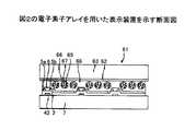
図2には、図1に示した有機トランジスタを用いた電子素子アレイの一例を示す。図2(a)は断面図、図2(b)は電極等の配置関係の平面図である。本発明の材料から作製される濡れ性変化膜を用いて、電子素子アレイの電極配線の取り出し部分も作製可能であることは、容易に想到できる(図示せず)。 FIG. 2 shows an example of an electronic element array using the organic transistor shown in FIG. 2A is a cross-sectional view, and FIG. 2B is a plan view of the arrangement relationship of electrodes and the like. It can be easily conceived that an electrode wiring take-out portion of an electronic element array can be produced using a wettability changing film produced from the material of the present invention (not shown).
図3は、図2に示した電子素子アレイを用いた表示装置を示す断面図である。ここでは、オイルブルーで着色したアイソパーと酸化チタン粒子をカプセルで包んだ電気泳動型表示装置が示されている。表示装置は電気泳動型でなくても、例えばポリマー分散型液晶でも良い。また、表示色材料はどのような色でも良い。 FIG. 3 is a cross-sectional view showing a display device using the electronic element array shown in FIG. Here, an electrophoretic display device in which Isopar colored with oil blue and titanium oxide particles are encapsulated is shown. The display device may not be an electrophoretic type but may be a polymer dispersed liquid crystal, for example. The display color material may be any color.
図4は、図3に示した表示装置を表示媒体として用いたデジタルペーパーの模式図である。また図5に示したように、ポケットPCのようなコンピューター等に表示媒体を実装して用いることも可能である。なお、図4ならびに図5は、画像表示装置の一例を説明するための模式図であり、例えば複写機の表示媒体に用いたり、自動車や飛行機などの移動交通媒体のシート部やフロントガラス面などに埋め込み、表示媒体として用いたり、スーパーなどで価格を表示するタグとして用いることも可能である。 FIG. 4 is a schematic diagram of digital paper using the display device shown in FIG. 3 as a display medium. As shown in FIG. 5, it is also possible to use a display medium mounted on a computer such as a pocket PC. 4 and 5 are schematic diagrams for explaining an example of the image display device. For example, the image display device is used as a display medium of a copying machine, or a sheet portion or a windshield surface of a mobile traffic medium such as an automobile or an airplane. It can also be used as a display medium, or as a tag for displaying the price at a supermarket.
一方で、本発明であるデンドロン側鎖を有する官能性ジアミン化合物を用いて合成されたポリイミド膜は、撥水性の側鎖(炭化水素鎖あるいはハロゲン鎖)が主鎖から出ていることから、側鎖を空気中に向けた(膜面内ではない方向)構造を容易にとることが推測される。よって、ラビングなどの手法により、この膜上に接する液晶分子を容易に配向させられること、それも垂直配向させられると想像できる。すなわち、液晶配向膜(垂直配向膜)としても高い潜在能力を持っていると考えら得る。また、本発明によると、デンドロン側鎖を有する官能性ジアミン化合物は、エネルギーの付与により表面自由エネルギーの改変が可能な膜表面を提供することができる。よって、例えば、有機電界発光素子(有機EL素子)などのポリイミドバンクとして用いることも可能である。 On the other hand, the polyimide film synthesized using the functional diamine compound having a dendron side chain according to the present invention has a water-repellent side chain (hydrocarbon chain or halogen chain) from the main chain. It is presumed that a structure in which the chain is directed in the air (in a direction not in the film plane) is easily taken. Therefore, it can be imagined that liquid crystal molecules in contact with this film can be easily aligned by a technique such as rubbing, and that it can also be vertically aligned. That is, it can be considered that the liquid crystal alignment film (vertical alignment film) has high potential. Moreover, according to the present invention, the functional diamine compound having a dendron side chain can provide a film surface capable of modifying the surface free energy by applying energy. Therefore, for example, it can also be used as a polyimide bank such as an organic electroluminescent element (organic EL element).
(実施例)
本発明を、以下の実施例により、さらに詳細に説明する。しかしながら、これらの実施例は説明のために示されるものであり、本発明の範囲を何ら制限するものではない。
(1)酸クロリド(12)の調製
下記の反応式に従って酸クロリド(12)を調整した。(Example)
The invention is illustrated in more detail by the following examples. However, these examples are provided for the purpose of illustration and are not intended to limit the scope of the present invention.
(1) Preparation of acid chloride (12) Acid chloride (12) was prepared according to the following reaction formula.
コンデンサを取り付けた丸底フラスコ中で、1モルの置換安息香酸エステル(1)と、炭酸カリウム8.97モルとを溶媒ジメチルホルムアミド(DMF)中に加え十分に攪拌した。この溶液に3モルの臭化ドデカン(9)を加えた後、少しずつフラスコの反応温度を上げて70℃とした。その後、反応混合物を70℃に保ちながら反応を24時間続けた。反応完了後、温度を室温へと下げた。反応溶液を純水に注いで沈殿物を形成した。この沈殿物をろ過し、洗浄を繰り返してドデカン付加物(10)を得た。得られたドデカン付加物(10)をエタノールに溶解した後、水酸化カリウムをこれに加えた。エタノール溶液を4時間還流して酸誘導体(11)を得た。この酸誘導体(11)を塩化チオニルとジクロロメタンと共に4時間還流することにより塩素化して酸クロリド(12)を得た。 In a round bottom flask equipped with a condenser, 1 mol of substituted benzoic acid ester (1) and 8.97 mol of potassium carbonate were added to the solvent dimethylformamide (DMF) and stirred sufficiently. After 3 mol of dodecane bromide (9) was added to this solution, the reaction temperature of the flask was gradually raised to 70 ° C. The reaction was then continued for 24 hours while maintaining the reaction mixture at 70 ° C. After the reaction was complete, the temperature was lowered to room temperature. The reaction solution was poured into pure water to form a precipitate. This precipitate was filtered and washed repeatedly to obtain a dodecane adduct (10). The obtained dodecane adduct (10) was dissolved in ethanol, and potassium hydroxide was added thereto. The ethanol solution was refluxed for 4 hours to obtain an acid derivative (11). This acid derivative (11) was chlorinated by refluxing with thionyl chloride and dichloromethane for 4 hours to obtain acid chloride (12).
(2)ジアミン(17)の調製
下記の反応式に従ってジアミン(17)を調整した。(2) Preparation of diamine (17) Diamine (17) was prepared according to the following reaction formula.
十分に乾燥させた丸底フラスコ中に、1モルのヒドロキノン(13)と触媒であるトリエチルアミンをTHFに溶解させた。この溶液に調整しておいた酸クロリド(12)1モルをゆっくり滴下し、アイスバスで冷却しながら3時間攪拌し、中間体(14)を得た。中間体(14)をTHF中に溶解し、触媒としてトリエチルアミンをこれに加えた。この溶液に3,5−ジニトロベンゾイルクロリド(15)1モルを加えた。得られた混合物を室温にて3時間反応させてジニトロ化合物(16)を得た。次に、十分に洗浄して乾燥させた丸底フラスコの内部に存在する水分と酸素を真空除去し、代わりに不活性ガスとしてアルゴン(Ar)をフラスコに充填した。ジニトロ化合物(16)をフラスコに投入した後、エタノールとTHFの混合溶媒を加えてジニトロ化合物(16)を溶解した。触媒としてパラジウムカーボンを加え、0.3MPa、室温にて5時間接触水素還元を行った。反応完了後、カラムクロマトグラフィー及び再結晶により反応生成物を精製し、最終製品であるジアミン(17)を得た。 In a fully dried round bottom flask, 1 mol of hydroquinone (13) and triethylamine as a catalyst were dissolved in THF. 1 mol of acid chloride (12) prepared in this solution was slowly added dropwise and stirred for 3 hours while cooling with an ice bath to obtain an intermediate (14). Intermediate (14) was dissolved in THF and triethylamine was added thereto as a catalyst. To this solution, 1 mol of 3,5-dinitrobenzoyl chloride (15) was added. The obtained mixture was reacted at room temperature for 3 hours to obtain a dinitro compound (16). Next, moisture and oxygen present in the round-bottomed flask that had been thoroughly washed and dried were removed in vacuum, and argon (Ar) as an inert gas was filled in the flask instead. After the dinitro compound (16) was added to the flask, a mixed solvent of ethanol and THF was added to dissolve the dinitro compound (16). Palladium carbon was added as a catalyst, and catalytic hydrogen reduction was performed at 0.3 MPa at room temperature for 5 hours. After completion of the reaction, the reaction product was purified by column chromatography and recrystallization to obtain the final product, diamine (17).
得られたジアミン(17)の構造を1H−NMRスペクトル並びにFT−IRスペクトルを用いて確認し、示差走査熱量測定法(DSC)を用いて熱的特性を評価した。この結果をそれぞれ図6、図7及び図8に示す。The structure of the obtained diamine (17) was confirmed using1 H-NMR spectrum and FT-IR spectrum, and the thermal characteristics were evaluated using differential scanning calorimetry (DSC). The results are shown in FIGS. 6, 7 and 8, respectively.
(実施例1)
撹拌器、サーモスタット、窒素注入装置およびコンデンサを取り付けた四ツ首フラスコに、窒素を通過させながら0.95モルの4,4'−メチレンジアニリン(18)および調整しておいた0.05モルのジアミン(17)を投入した。次にN−メチル−2−ピロリドン(NMP)溶液をこれに加え、得られた混合物を十分に溶解した。この溶液に、固体状態の0.5モルの5−(2,5−ジオキソテトラヒドロフリル)−3−メチルシクロヘキサン−1,2−ジカルボン酸二無水物(DOCDA)(19)および0.5モルのピロメリット酸二無水物(PMDA)(20)を加えた。得られた混合物を強力に撹拌した。この時点で固体含有率は15重量%であった。温度を25℃未満に保持しながら、反応混合物を24時間反応させてポリアミド酸溶液を調製した。Example 1
A four-necked flask equipped with a stirrer, thermostat, nitrogen injector and condenser was charged with 0.95 moles of 4,4′-methylenedianiline (18) and 0.05 moles prepared while passing nitrogen. Of diamine (17). N-methyl-2-pyrrolidone (NMP) solution was then added to it and the resulting mixture was fully dissolved. To this solution was added 0.5 mol of 5- (2,5-dioxotetrahydrofuryl) -3-methylcyclohexane-1,2-dicarboxylic dianhydride (DOCDA) (19) and 0.5 mol in the solid state. Of pyromellitic dianhydride (PMDA) (20) was added. The resulting mixture was stirred vigorously. At this point, the solid content was 15% by weight. While maintaining the temperature below 25 ° C., the reaction mixture was reacted for 24 hours to prepare a polyamic acid solution.
(比較例1)
0.95モルの4,4'−メチレンジアニリン(18)及び0.05モルのジアミン(17)に代えて、0.80モルの4,4'−メチレンジアニリン(18)及び0.20モルの2,4−ジアミノフェノキシヘキサデカン(21)を使用したことを除き、実施例1と同様の方法でポリアミド酸を調製した。実施例1に記載の手順に従って濡れ性変化薄膜(B)を作製し、同様に電極材料の接触角を測定した。その結果を表1に示す。(Comparative Example 1)
Instead of 0.95 mol of 4,4'-methylenedianiline (18) and 0.05 mol of diamine (17), 0.80 mol of 4,4'-methylenedianiline (18) and 0.20 mol A polyamic acid was prepared in the same manner as in Example 1 except that
(比較例2)
0.95モルの4,4'−メチレンジアニリン(18)及び0.05モルのジアミン(17)に代えて、0.95モルの4,4−メチレンジアニリン(18)および0.05モルのジアミン化合物(22)を使用したことを除き、実施例1と同様の方法でポリアミド酸を調製した。実施例1に記載の手順に従って濡れ性変化薄膜(C)を作製し、同様に電極材料の接触角を測定した。その結果を表1に示す。(Comparative Example 2)
Instead of 0.95
(実施例2)
続いて、電極パターニング性を比較した。実施例1で作製した濡れ性変化薄膜(A)に対して、ライン形状のフォトマスク越しに紫外線(高圧水銀ランプ)を照度1から15J/cm2となるように照射し、薄膜上に表面自由エネルギーの大きい部位を形成した。形成した表面自由エネルギーの大きい部位にインクジェット法を用いてナノ銀の電極材料インクを吐出した。210℃のオーブンで焼成した後、5μm間隔のラインが形成できているか金属顕微鏡観察により確認した。結果を表1に示す。(Example 2)
Subsequently, electrode patterning properties were compared. The wettability changing thin film (A) produced in Example 1 was irradiated with ultraviolet rays (high pressure mercury lamp) through a line-shaped photomask so that the illuminance was 1 to 15 J / cm2, and the surface was free on the thin film. A site with high energy was formed. A nano silver electrode material ink was ejected to the formed portion having a large surface free energy by using an ink jet method. After firing in an oven at 210 ° C., it was confirmed by observation with a metal microscope whether or not 5 μm-interval lines were formed. The results are shown in Table 1.
表1に示す電極パターニング性において、×は一つも5μm間隔のラインが形成できていなかったもの、△は何個かできていたもの、○は何個かできていないものがあったもの、◎は全てできているものを示す。 In the electrode patterning properties shown in Table 1, × indicates that no line having an interval of 5 μm was formed, Δ indicates that some were formed, ○ indicates that some were not formed, and ◎ Indicates everything that is made.
(比較例3)
比較例1で作製した濡れ性変化薄膜(B)上に、実施例2と同様にして紫外線を照射し、インクジェット法によりナノ銀インクを吐出した。焼成後、5μm間隔のラインが形成できているか金属顕微鏡観察により確認した。結果を表1に示す。(Comparative Example 3)
The wettability changing thin film (B) produced in Comparative Example 1 was irradiated with ultraviolet rays in the same manner as in Example 2, and nano silver ink was ejected by the inkjet method. After firing, it was confirmed by observation with a metallurgical microscope whether lines with an interval of 5 μm were formed. The results are shown in Table 1.
(比較例4)
比較例2で作製した濡れ性変化薄膜(C)上に、実施例2と同様にして紫外線を照射し、インクジェット法によりナノ銀インクを吐出した。焼成後、5μm間隔のラインが形成できているか金属顕微鏡観察により確認した。結果を表1に示す
これらの結果は、実施例1で得られた紫外線照射量と電極材料の接触角の結果に良好に対応している。すなわち、本発明の一例であるジアミン(17)から形成した濡れ性変化薄膜(A)では、紫外線照射量がたかだか2J/cm2から表面自由エネルギーの高い面が形成されるので、ここに親水性(表面自由エネルギーの高い)の電極材料をインクジェット塗布すると、表面自由エネルギーの高い面と低い面の境界ラインが鮮明に形成できる。表面自由エネルギーの高い面以外にはインクは濡れ拡がらず5μm間隔のラインが形成可能となる。一方、ジアミン(21)から形成した濡れ性変化薄膜(B)では、実験を行った15J/cm2まででは紫外線による接触角変化が5°程度と小さく、5μm間隔のラインを形成できなかった。
ところで、ジアミン(17)から形成した濡れ性変化薄膜(A)と同様に側鎖にデンドロン構造を有するジアミン(22)から形成した濡れ性変化薄膜(C)では、5J/cm2以上照射しないとエネルギーの高い面が形成されず、部分的に5μm間隔のラインが形成されていないところがある。ジアミン(17)から形成した濡れ性変化薄膜(A)よりも紫外線照射量が必要となるのは、π共役の拡がりが小さいためと考えられる。(Comparative Example 4)
The wettability changing thin film (C) produced in Comparative Example 2 was irradiated with ultraviolet rays in the same manner as in Example 2, and nano silver ink was ejected by the inkjet method. After firing, it was confirmed by observation with a metallurgical microscope whether lines with an interval of 5 μm were formed. The results are shown in Table 1. These results correspond well with the results of the ultraviolet irradiation amount obtained in Example 1 and the contact angle of the electrode material. That is, in the wettability changing thin film (A) formed from the diamine (17) as an example of the present invention, a surface having a high surface free energy is formed from an ultraviolet ray irradiation amount of2 J / cm2 at the most. When an electrode material having a high surface free energy is applied by ink jetting, a boundary line between a surface having a high surface free energy and a surface having a low surface free energy can be clearly formed. Other than the surface having a high surface free energy, the ink does not spread out and lines of 5 μm intervals can be formed. On the other hand, in the wettability changing thin film (B) formed from the diamine (21), the contact angle change due to ultraviolet rays was as small as about 5 ° up to 15 J / cm2 where the experiment was performed, and it was not possible to form lines with intervals of 5 μm.
By the way, the wettability change thin film (C) formed from the diamine (22) having a dendron structure in the side chain as in the wettability change thin film (A) formed from the diamine (17) must be irradiated with 5 J / cm2 or more. There is a place where a surface with high energy is not formed and a line having a space of 5 μm is not partially formed. The reason why the UV irradiation amount is required to be greater than the wettability changing thin film (A) formed from the diamine (17) is considered to be because the spread of π conjugate is small.
このように、側鎖にデンドロン構造を有し、且つ、長波長の紫外線の吸収部位が複数含まれる構造体では、より少ない紫外線照射量で、電極が形成できることが分かる。 Thus, it can be seen that in a structure having a dendron structure in the side chain and including a plurality of long-wavelength ultraviolet absorption sites, an electrode can be formed with a smaller amount of ultraviolet irradiation.
1 高絶縁層
2 濡れ性変化層
3 臨界表面張力の大きな高表面エネルギー部
4 臨界表面張力の小さな低表面エネルギー部
5 導電層
5a ソース電極層
5b ドレイン電極層
6 半導体層
7 基板
41 電子素子
42 ゲート電極
51 電子素子アレイ
61 表示装置
62 透明電極
63 ポリエチレンナフタレート基板
65 酸化チタン粒子
66 オイルブルーで着色したアイソパー
67 マイクロカプセル
68 PVAバインダーDESCRIPTION OF
Claims (11)
Translated fromJapanesePriority Applications (7)
| Application Number | Priority Date | Filing Date | Title |
|---|---|---|---|
| JP2007178703AJP5239231B2 (en) | 2007-07-06 | 2007-07-06 | Diamine compound, polyamic acid and soluble polyimide, and wettability changing film and electrode obtained therefrom |
| KR1020097027479AKR20100020014A (en) | 2007-07-06 | 2008-07-04 | Diamine compound, polyamic acid, soluble polyimide, composition, wettability changing film, electrode, and method of manufacturing a wettability changing film |
| EP08778051.6AEP2162484B1 (en) | 2007-07-06 | 2008-07-04 | Polyamic acid |
| US12/667,390US20100184936A1 (en) | 2007-07-06 | 2008-07-04 | Diamine compound, polyamic acid, soluble polyimide, composition, wettability changing film, electrode, and method of manufacturing a wettability changing film |
| PCT/JP2008/062530WO2009008491A1 (en) | 2007-07-06 | 2008-07-04 | Diamine compound, polyamic acid, soluble polyimide, composition, wettability changing film, electrode, and method of manufacturing a wettability changing film |
| CN2008800227003ACN101687992B (en) | 2007-07-06 | 2008-07-04 | Diamine compound and polyamic acid |
| TW097125563ATWI438902B (en) | 2007-07-06 | 2008-07-07 | Diamine compound, polyamic acid, soluble polyimide, composition, wettability changing film, electrode, and method of manufacturing a wettability changing film |
Applications Claiming Priority (1)
| Application Number | Priority Date | Filing Date | Title |
|---|---|---|---|
| JP2007178703AJP5239231B2 (en) | 2007-07-06 | 2007-07-06 | Diamine compound, polyamic acid and soluble polyimide, and wettability changing film and electrode obtained therefrom |
Publications (2)
| Publication Number | Publication Date |
|---|---|
| JP2009013342A JP2009013342A (en) | 2009-01-22 |
| JP5239231B2true JP5239231B2 (en) | 2013-07-17 |
Family
ID=40228662
Family Applications (1)
| Application Number | Title | Priority Date | Filing Date |
|---|---|---|---|
| JP2007178703AActiveJP5239231B2 (en) | 2007-07-06 | 2007-07-06 | Diamine compound, polyamic acid and soluble polyimide, and wettability changing film and electrode obtained therefrom |
Country Status (7)
| Country | Link |
|---|---|
| US (1) | US20100184936A1 (en) |
| EP (1) | EP2162484B1 (en) |
| JP (1) | JP5239231B2 (en) |
| KR (1) | KR20100020014A (en) |
| CN (1) | CN101687992B (en) |
| TW (1) | TWI438902B (en) |
| WO (1) | WO2009008491A1 (en) |
Families Citing this family (7)
| Publication number | Priority date | Publication date | Assignee | Title |
|---|---|---|---|---|
| JP5446751B2 (en)* | 2009-03-18 | 2014-03-19 | 株式会社リコー | Multilayer structure, electronic element, electronic element array, image display medium, and image display apparatus |
| JP5397017B2 (en)* | 2009-05-25 | 2014-01-22 | 株式会社リコー | Polyamide acid and polyimide |
| TWI422573B (en)* | 2010-02-11 | 2014-01-11 | Nat Univ Tsing Hua | Organic thin film transistor and method of preparing the same |
| JP5662985B2 (en) | 2011-11-02 | 2015-02-04 | 富士フイルム株式会社 | Conductive pattern-forming substrate, circuit board and method for producing them |
| JP6197418B2 (en) | 2013-07-05 | 2017-09-20 | 株式会社リコー | Method for forming multilayer wiring, multilayer wiring, and electronic device |
| CN106750292A (en)* | 2016-12-28 | 2017-05-31 | 杭州福斯特光伏材料股份有限公司 | A kind of polyimides for printed electronic |
| CN106898434B (en)* | 2017-02-28 | 2018-08-10 | 厦门大学 | A kind of manufacturing method of conductive heater transparent electrode |
Family Cites Families (13)
| Publication number | Priority date | Publication date | Assignee | Title |
|---|---|---|---|---|
| US3647805A (en)* | 1969-07-11 | 1972-03-07 | Kyorin Seiyaku Kk | Benzoylamino substituted 1-benzoyl-piperidines |
| JPH06345869A (en)* | 1993-06-03 | 1994-12-20 | Shin Etsu Chem Co Ltd | Polyimide and manufacturing method thereof |
| JPH10298164A (en)* | 1997-02-27 | 1998-11-10 | Tanabe Seiyaku Co Ltd | Isoquinolinone derivative, its production method and its synthetic intermediate |
| AU6230098A (en)* | 1997-02-27 | 1998-09-18 | Tanabe Seiyaku Co., Ltd. | Isoquinolinone derivatives, process for preparing the same, and their use as phosphodiesterase inhibitors |
| KR100292830B1 (en) | 1998-09-17 | 2001-07-12 | 김덕중 | Organic light-emitting device having improved luminous efficiency |
| CN1174081C (en) | 2001-03-20 | 2004-11-03 | 四川大学 | Preparation method of side chain liquid crystal polyimide film |
| KR100599859B1 (en)* | 2003-10-09 | 2006-07-12 | 제일모직주식회사 | Diamine compound having side chain of dendron structure and liquid crystal aligning material manufactured using the same |
| US20060014029A1 (en)* | 2004-07-15 | 2006-01-19 | General Electric Company | Article including environmental barrier coating system, and method for making |
| JP5209844B2 (en)* | 2004-11-30 | 2013-06-12 | 株式会社リコー | ELECTRONIC DEVICE AND METHOD FOR MANUFACTURING THE SAME, OPERATION ELEMENT AND DISPLAY ELEMENT |
| KR100715095B1 (en) | 2004-12-31 | 2007-05-04 | 제일모직주식회사 | Diamine compound having side chain of dendron structure and liquid crystal aligning material using the same |
| JP4994727B2 (en)* | 2005-09-08 | 2012-08-08 | 株式会社リコー | Organic transistor active substrate, manufacturing method thereof, and electrophoretic display using the organic transistor active substrate |
| JP2007150246A (en)* | 2005-11-02 | 2007-06-14 | Ricoh Co Ltd | Organic transistor and display device |
| JP5167707B2 (en)* | 2006-08-04 | 2013-03-21 | 株式会社リコー | Multilayer structure, multilayer wiring board, active matrix substrate, and electronic display device |
- 2007
- 2007-07-06JPJP2007178703Apatent/JP5239231B2/enactiveActive
- 2008
- 2008-07-04CNCN2008800227003Apatent/CN101687992B/ennot_activeExpired - Fee Related
- 2008-07-04EPEP08778051.6Apatent/EP2162484B1/ennot_activeNot-in-force
- 2008-07-04WOPCT/JP2008/062530patent/WO2009008491A1/enactiveApplication Filing
- 2008-07-04USUS12/667,390patent/US20100184936A1/ennot_activeAbandoned
- 2008-07-04KRKR1020097027479Apatent/KR20100020014A/ennot_activeCeased
- 2008-07-07TWTW097125563Apatent/TWI438902B/ennot_activeIP Right Cessation
Also Published As
| Publication number | Publication date |
|---|---|
| WO2009008491A1 (en) | 2009-01-15 |
| JP2009013342A (en) | 2009-01-22 |
| EP2162484B1 (en) | 2019-02-27 |
| EP2162484A4 (en) | 2011-11-23 |
| EP2162484A1 (en) | 2010-03-17 |
| TWI438902B (en) | 2014-05-21 |
| US20100184936A1 (en) | 2010-07-22 |
| KR20100020014A (en) | 2010-02-19 |
| TW200908340A (en) | 2009-02-16 |
| CN101687992A (en) | 2010-03-31 |
| CN101687992B (en) | 2012-04-11 |
Similar Documents
| Publication | Publication Date | Title |
|---|---|---|
| JP5239231B2 (en) | Diamine compound, polyamic acid and soluble polyimide, and wettability changing film and electrode obtained therefrom | |
| JP4629997B2 (en) | Thin film transistor and thin film transistor array | |
| JP5211729B2 (en) | Laminated structure and manufacturing method thereof | |
| CN101199041B (en) | Electrode pattern forming layer, method of manufacturing the same, pattern electrode, electronic device, and organic FET | |
| JP4027384B2 (en) | Insulating film containing soluble polyimide resin and all-organic thin-film transistor using the same | |
| WO2007078153A1 (en) | Composition for liquid crystal aligning, liquid crystal aligning layer prepared from the same, and liquid crystal display comprising the same | |
| JPWO2019103042A1 (en) | Liquid crystal alignment agent, liquid crystal alignment film, manufacturing method of liquid crystal alignment film, and liquid crystal display element | |
| JP5397017B2 (en) | Polyamide acid and polyimide | |
| JP5532259B2 (en) | Underlayer film for image formation | |
| JP2006060113A (en) | LAMINATED STRUCTURE, ELECTRONIC DEVICE USING LAMINATED STRUCTURE, METHOD FOR MANUFACTURING THE SAME, ELECTRONIC DEVICE ARRAY, AND DISPLAY DEVICE | |
| JP2006060113A5 (en) | ||
| KR20040046229A (en) | Photosensitive colorless polyamic acids derivatives and polyimides | |
| KR100831155B1 (en) | Composition for liquid crystal aligning, liquid crystal aligning layer manufactured by the same, and liquid crystal display comprising the same | |
| JPWO2010047346A6 (en) | Underlayer film for image formation | |
| JP5899668B2 (en) | Laminated structure and manufacturing method thereof | |
| KR20130004069A (en) | Diamine compound, method for preparing the same, liquid crystal alignment agent, liquid crystal alignment film and liquid crystal display device | |
| KR101187609B1 (en) | Low temperature processable and photo-crosslinkable organic gate insulator, and organic thin film transistor device using the same | |
| KR100552989B1 (en) | Photosensitive polyamic acid derivatives and polyimides for insulator of organic thin film transistor | |
| US20020048719A1 (en) | Ion-type photoacid generator containing naphthol and photosensitive polyimide composition prepared by using the same | |
| KR20090066077A (en) | Novel photodiamine, and liquid crystal photoalignment agent, liquid crystal photoalignment film, and liquid crystal display device including the same | |
| KR100562524B1 (en) | Polyimide Resin Prepared by Curing Photosensitive Transparent Polyamic Acid Oligomers with Excellent Flattening Properties | |
| KR101411830B1 (en) | Low temperature processable and photo-crosslinkable organic gate insulator, and organic thin film transistor device using the same | |
| JP4906934B2 (en) | Electronic element, electronic element array, and display device | |
| CN119371347A (en) | Photosensitive compound, resin composition, cured film and electronic device | |
| CN120418384A (en) | Composition for forming liquid crystal alignment film |
Legal Events
| Date | Code | Title | Description |
|---|---|---|---|
| A621 | Written request for application examination | Free format text:JAPANESE INTERMEDIATE CODE: A621 Effective date:20100222 | |
| A131 | Notification of reasons for refusal | Free format text:JAPANESE INTERMEDIATE CODE: A131 Effective date:20121120 | |
| A521 | Request for written amendment filed | Free format text:JAPANESE INTERMEDIATE CODE: A523 Effective date:20130121 | |
| TRDD | Decision of grant or rejection written | ||
| A01 | Written decision to grant a patent or to grant a registration (utility model) | Free format text:JAPANESE INTERMEDIATE CODE: A01 Effective date:20130305 | |
| A61 | First payment of annual fees (during grant procedure) | Free format text:JAPANESE INTERMEDIATE CODE: A61 Effective date:20130318 | |
| FPAY | Renewal fee payment (event date is renewal date of database) | Free format text:PAYMENT UNTIL: 20160412 Year of fee payment:3 | |
| R151 | Written notification of patent or utility model registration | Ref document number:5239231 Country of ref document:JP Free format text:JAPANESE INTERMEDIATE CODE: R151 | |
| FPAY | Renewal fee payment (event date is renewal date of database) | Free format text:PAYMENT UNTIL: 20160412 Year of fee payment:3 |