JP5226438B2 - Substrate processing apparatus, semiconductor device manufacturing method, and substrate processing method - Google Patents
Substrate processing apparatus, semiconductor device manufacturing method, and substrate processing methodDownload PDFInfo
- Publication number
- JP5226438B2 JP5226438B2JP2008232618AJP2008232618AJP5226438B2JP 5226438 B2JP5226438 B2JP 5226438B2JP 2008232618 AJP2008232618 AJP 2008232618AJP 2008232618 AJP2008232618 AJP 2008232618AJP 5226438 B2JP5226438 B2JP 5226438B2
- Authority
- JP
- Japan
- Prior art keywords
- gas
- processing
- substrate
- processing chamber
- booster pump
- Prior art date
- Legal status (The legal status is an assumption and is not a legal conclusion. Google has not performed a legal analysis and makes no representation as to the accuracy of the status listed.)
- Expired - Fee Related
Links
Images


Classifications
- C—CHEMISTRY; METALLURGY
- C23—COATING METALLIC MATERIAL; COATING MATERIAL WITH METALLIC MATERIAL; CHEMICAL SURFACE TREATMENT; DIFFUSION TREATMENT OF METALLIC MATERIAL; COATING BY VACUUM EVAPORATION, BY SPUTTERING, BY ION IMPLANTATION OR BY CHEMICAL VAPOUR DEPOSITION, IN GENERAL; INHIBITING CORROSION OF METALLIC MATERIAL OR INCRUSTATION IN GENERAL
- C23C—COATING METALLIC MATERIAL; COATING MATERIAL WITH METALLIC MATERIAL; SURFACE TREATMENT OF METALLIC MATERIAL BY DIFFUSION INTO THE SURFACE, BY CHEMICAL CONVERSION OR SUBSTITUTION; COATING BY VACUUM EVAPORATION, BY SPUTTERING, BY ION IMPLANTATION OR BY CHEMICAL VAPOUR DEPOSITION, IN GENERAL
- C23C16/00—Chemical coating by decomposition of gaseous compounds, without leaving reaction products of surface material in the coating, i.e. chemical vapour deposition [CVD] processes
- C23C16/22—Chemical coating by decomposition of gaseous compounds, without leaving reaction products of surface material in the coating, i.e. chemical vapour deposition [CVD] processes characterised by the deposition of inorganic material, other than metallic material
- C23C16/24—Deposition of silicon only
- C—CHEMISTRY; METALLURGY
- C23—COATING METALLIC MATERIAL; COATING MATERIAL WITH METALLIC MATERIAL; CHEMICAL SURFACE TREATMENT; DIFFUSION TREATMENT OF METALLIC MATERIAL; COATING BY VACUUM EVAPORATION, BY SPUTTERING, BY ION IMPLANTATION OR BY CHEMICAL VAPOUR DEPOSITION, IN GENERAL; INHIBITING CORROSION OF METALLIC MATERIAL OR INCRUSTATION IN GENERAL
- C23C—COATING METALLIC MATERIAL; COATING MATERIAL WITH METALLIC MATERIAL; SURFACE TREATMENT OF METALLIC MATERIAL BY DIFFUSION INTO THE SURFACE, BY CHEMICAL CONVERSION OR SUBSTITUTION; COATING BY VACUUM EVAPORATION, BY SPUTTERING, BY ION IMPLANTATION OR BY CHEMICAL VAPOUR DEPOSITION, IN GENERAL
- C23C16/00—Chemical coating by decomposition of gaseous compounds, without leaving reaction products of surface material in the coating, i.e. chemical vapour deposition [CVD] processes
- C23C16/22—Chemical coating by decomposition of gaseous compounds, without leaving reaction products of surface material in the coating, i.e. chemical vapour deposition [CVD] processes characterised by the deposition of inorganic material, other than metallic material
- C23C16/30—Deposition of compounds, mixtures or solid solutions, e.g. borides, carbides, nitrides
- C—CHEMISTRY; METALLURGY
- C23—COATING METALLIC MATERIAL; COATING MATERIAL WITH METALLIC MATERIAL; CHEMICAL SURFACE TREATMENT; DIFFUSION TREATMENT OF METALLIC MATERIAL; COATING BY VACUUM EVAPORATION, BY SPUTTERING, BY ION IMPLANTATION OR BY CHEMICAL VAPOUR DEPOSITION, IN GENERAL; INHIBITING CORROSION OF METALLIC MATERIAL OR INCRUSTATION IN GENERAL
- C23C—COATING METALLIC MATERIAL; COATING MATERIAL WITH METALLIC MATERIAL; SURFACE TREATMENT OF METALLIC MATERIAL BY DIFFUSION INTO THE SURFACE, BY CHEMICAL CONVERSION OR SUBSTITUTION; COATING BY VACUUM EVAPORATION, BY SPUTTERING, BY ION IMPLANTATION OR BY CHEMICAL VAPOUR DEPOSITION, IN GENERAL
- C23C16/00—Chemical coating by decomposition of gaseous compounds, without leaving reaction products of surface material in the coating, i.e. chemical vapour deposition [CVD] processes
- C23C16/44—Chemical coating by decomposition of gaseous compounds, without leaving reaction products of surface material in the coating, i.e. chemical vapour deposition [CVD] processes characterised by the method of coating
- C23C16/4412—Details relating to the exhausts, e.g. pumps, filters, scrubbers, particle traps
- C—CHEMISTRY; METALLURGY
- C30—CRYSTAL GROWTH
- C30B—SINGLE-CRYSTAL GROWTH; UNIDIRECTIONAL SOLIDIFICATION OF EUTECTIC MATERIAL OR UNIDIRECTIONAL DEMIXING OF EUTECTOID MATERIAL; REFINING BY ZONE-MELTING OF MATERIAL; PRODUCTION OF A HOMOGENEOUS POLYCRYSTALLINE MATERIAL WITH DEFINED STRUCTURE; SINGLE CRYSTALS OR HOMOGENEOUS POLYCRYSTALLINE MATERIAL WITH DEFINED STRUCTURE; AFTER-TREATMENT OF SINGLE CRYSTALS OR A HOMOGENEOUS POLYCRYSTALLINE MATERIAL WITH DEFINED STRUCTURE; APPARATUS THEREFOR
- C30B25/00—Single-crystal growth by chemical reaction of reactive gases, e.g. chemical vapour-deposition growth
- C30B25/02—Epitaxial-layer growth
- C30B25/14—Feed and outlet means for the gases; Modifying the flow of the reactive gases
- C—CHEMISTRY; METALLURGY
- C30—CRYSTAL GROWTH
- C30B—SINGLE-CRYSTAL GROWTH; UNIDIRECTIONAL SOLIDIFICATION OF EUTECTIC MATERIAL OR UNIDIRECTIONAL DEMIXING OF EUTECTOID MATERIAL; REFINING BY ZONE-MELTING OF MATERIAL; PRODUCTION OF A HOMOGENEOUS POLYCRYSTALLINE MATERIAL WITH DEFINED STRUCTURE; SINGLE CRYSTALS OR HOMOGENEOUS POLYCRYSTALLINE MATERIAL WITH DEFINED STRUCTURE; AFTER-TREATMENT OF SINGLE CRYSTALS OR A HOMOGENEOUS POLYCRYSTALLINE MATERIAL WITH DEFINED STRUCTURE; APPARATUS THEREFOR
- C30B29/00—Single crystals or homogeneous polycrystalline material with defined structure characterised by the material or by their shape
- C30B29/02—Elements
- C30B29/06—Silicon
Landscapes
- Chemical & Material Sciences (AREA)
- Engineering & Computer Science (AREA)
- Materials Engineering (AREA)
- Metallurgy (AREA)
- Organic Chemistry (AREA)
- General Chemical & Material Sciences (AREA)
- Chemical Kinetics & Catalysis (AREA)
- Mechanical Engineering (AREA)
- Crystallography & Structural Chemistry (AREA)
- Inorganic Chemistry (AREA)
- Chemical Vapour Deposition (AREA)
Description
Translated fromJapanese本発明は、基板を処理する基板処理装置に関する。 The present invention relates to a substrate processing apparatus for processing a substrate.
エピタキシャルシリコン膜(Epi−Si膜)やエピタキシャルシリコンゲルマニウム膜(Epi−SiGe膜)等の膜は、基板を収容した処理室内に処理ガス(プロセスガス)を供給することにより成長させることができる。なお、エピタキシャル膜の成長に際しては、処理室内への処理ガスの供給流量を安定させることが必要となる場合がある。かかる場合、処理室内に処理ガスを供給する前に、ガス供給系に設けられたバイパス配管から処理ガスを排気することにより、ガス供給系からの処理ガスの供給流量を安定させていた。 A film such as an epitaxial silicon film (Epi-Si film) or an epitaxial silicon germanium film (Epi-SiGe film) can be grown by supplying a processing gas (process gas) into a processing chamber containing the substrate. Note that when the epitaxial film is grown, it may be necessary to stabilize the supply flow rate of the processing gas into the processing chamber. In this case, the supply flow rate of the processing gas from the gas supply system is stabilized by exhausting the processing gas from the bypass piping provided in the gas supply system before supplying the processing gas into the processing chamber.
従来の基板処理装置においては、バイパス配管の下流側は、処理室内を排気するガス排気系に設けられた真空ポンプの上流側に接続されていた。ガス排気系の真空ポンプは、例えば上流から順に設けられたメカニカルブースタポンプとドライポンプとから構成されており、例えば3万slmでの排気が可能なように構成されていた。 In the conventional substrate processing apparatus, the downstream side of the bypass pipe is connected to the upstream side of the vacuum pump provided in the gas exhaust system for exhausting the processing chamber. The vacuum pump of the gas exhaust system is composed of, for example, a mechanical booster pump and a dry pump provided in order from the upstream, and is configured to be able to exhaust at, for example, 30,000 slm.
しかしながら、処理ガスをバイパス配管から排気させると、バイパス配管からガス排気系へと流れた処理ガスが、処理室内へと瞬間的に逆拡散(逆流)してしまう場合があった。その結果、ガス排気系内に残留していた異物等が処理ガスと共に処理室内に侵入してしまい、基板処理の品質低下や歩留り悪化を招いてしまう場合があった。処理室内への逆拡散を回避するには、バイパス配管の下流側をガス排気系に接続せず、バイパス配管の下流側に専用の真空ポンプを設ける構成も考えられる。しかしながら、かかる場合には基板処理装置の構成が複雑化してしまい、基板処理装置のコストや設置スペース(フットプリント)が増大してしまう場合があった。 However, when the processing gas is exhausted from the bypass pipe, the processing gas that has flowed from the bypass pipe to the gas exhaust system may instantaneously reversely diffuse (reverse flow) into the processing chamber. As a result, foreign matter or the like remaining in the gas exhaust system may enter the processing chamber together with the processing gas, leading to a decrease in substrate processing quality and yield. In order to avoid back diffusion into the processing chamber, a configuration in which a dedicated vacuum pump is provided on the downstream side of the bypass pipe without connecting the downstream side of the bypass pipe to the gas exhaust system is also conceivable. However, in such a case, the configuration of the substrate processing apparatus becomes complicated, and the cost and installation space (footprint) of the substrate processing apparatus may increase.
そこで本発明は、バイパス配管の下流側に専用の真空ポンプを設けることなく、バイパス配管からガス排気系へと排気された処理ガスの処理室内への逆拡散を抑制することが可能な基板処理装置を提供することを目的とする。 Therefore, the present invention provides a substrate processing apparatus capable of suppressing the back diffusion of the processing gas exhausted from the bypass pipe to the gas exhaust system into the processing chamber without providing a dedicated vacuum pump downstream of the bypass pipe. The purpose is to provide.
本発明の一態様によれば、基板を収容する処理室と、前記基板を処理する処理ガスを処理ガス源から前記処理室内へ供給するガス供給系と、前記処理室内の雰囲気を排気するガス排気系と、前記ガス排気系に直列に設けられた少なくとも2つの真空ポンプと、前記ガス供給系と前記ガス排気系とを前記処理室を介さずに接続するバイパス配管と、を含み、前記真空ポンプの内、前記ガス排気系を流れるガスの最上流側に位置する真空ポンプはメカニカルブースタポンプであって、前記バイパス配管は、前記メカニカルブースタポンプとその下流に位置する真空ポンプとの間の位置に接続される基板処理装置が提供される。 According to one aspect of the present invention, a processing chamber that accommodates a substrate, a gas supply system that supplies a processing gas for processing the substrate from a processing gas source to the processing chamber, and a gas exhaust that exhausts an atmosphere in the processing chamber And a bypass pipe for connecting the gas supply system and the gas exhaust system without going through the processing chamber, the vacuum pump comprising: a system; at least two vacuum pumps provided in series with the gas exhaust system; Among them, the vacuum pump located on the most upstream side of the gas flowing through the gas exhaust system is a mechanical booster pump, and the bypass pipe is located between the mechanical booster pump and a vacuum pump located downstream thereof. A connected substrate processing apparatus is provided.
本発明にかかる基板処理装置によれば、バイパス配管の下流側に専用の真空ポンプを設けることなく、バイパス配管からガス排気系へと排気された処理ガスの処理室内への逆拡散を抑制することが可能となる。 According to the substrate processing apparatus of the present invention, it is possible to suppress the back diffusion of the processing gas exhausted from the bypass pipe to the gas exhaust system into the processing chamber without providing a dedicated vacuum pump on the downstream side of the bypass pipe. Is possible.
上述したように、Epi−Si膜やEpi−SiGe膜は、基板を収容した処理室内に処理ガスを供給することにより成長させることができる。エピタキシャル膜を成長させる際には、Poly−Si膜等の多結晶膜を成長させるときに比べて、処理ガスの供給流量について高い安定性が求められる場合がある。 As described above, the Epi-Si film or Epi-SiGe film can be grown by supplying a processing gas into a processing chamber in which a substrate is accommodated. When the epitaxial film is grown, higher stability may be required for the supply flow rate of the processing gas than when a polycrystalline film such as a Poly-Si film is grown.
例えば、シリコン基板上にEpi−SiGe膜を成長させるには、処理室内に例えばSiH4ガスやSi2H6ガス等のシラン系ガス、GeH4ガス等のゲルマン系ガス、あるいはCl2ガス等の塩素系ガスを順次あるいは同時に供給するが、SiとGeの比率を正確に制御するには処理室201内に供給する各種ガスの流量を安定させる必要がある。また、Epi−SiGe膜に所定量のホウ素(B)元素をドープするには、処理室内に例えばH2ガスで希釈したB2H6ガスをさらに供給するが、Bのドープ量を正確に制御するには処理室内に供給する各種ガスの流量を同様に安定させる必要がある。また、Epi−Si膜を成長させるには、処理室内にSiH4ガスやSi2H6ガス等のシラン系ガスを供給した後、処理室201内にCl2ガスを短時間(例えば30秒)供給する工程を繰り返すが、かかる方法においても処理室内へのCl2ガスの供給流量を安定させる必要がある。For example, to grow an Epi-SiGe film on a silicon substrate, for example, a silane-based gas such as SiH4 gas or Si2 H6 gas, a germane gas such as GeH4 gas, or a Cl2 gas is used in the processing chamber. Chlorine-based gases are supplied sequentially or simultaneously. To accurately control the ratio of Si and Ge, it is necessary to stabilize the flow rates of various gases supplied into the
処理ガスの供給流量を安定させるには、処理室内への処理ガスの供給を開始する前に、ガス供給系に設けられたバイパス配管から処理ガスを排気してやることが有効である。バイパス配管から処理ガスを排気することにより、ガス供給系からの処理ガスの供給流量が供給開始直後に一時的に過大になってしまうオーバーシュート(over shoot)現象等を収束させることができる。オーバーシュート収束後に処理室内への処理ガスの供給を開始することにより、処理室内への処理ガスの供給流量を安定させることができる。 In order to stabilize the supply flow rate of the processing gas, it is effective to exhaust the processing gas from a bypass pipe provided in the gas supply system before starting the supply of the processing gas into the processing chamber. By exhausting the processing gas from the bypass pipe, it is possible to converge an overshoot phenomenon or the like in which the supply flow rate of the processing gas from the gas supply system becomes temporarily excessive immediately after the start of supply. By starting the supply of the processing gas into the processing chamber after the overshoot has converged, the supply flow rate of the processing gas into the processing chamber can be stabilized.
しかしながら、発明者等の鋭意研究によれば、従来の基板処理装置の構成では、処理ガスをバイパス配管から排気させようとすると、バイパス配管からガス排気系へ流れた処理ガスが、ガス排気系の下流側に流れずに処理室内へと瞬間的に逆拡散(逆流)してしまう場合があることが判明した。発明者等は、処理ガスの逆拡散を抑制する方法について鋭意研究を行った結果、バイパス配管の下流側の接続先を工夫することにより、上述の課題を解決可能であるとの知見を得た。 However, according to the diligent research by the inventors, in the configuration of the conventional substrate processing apparatus, when the processing gas is exhausted from the bypass pipe, the processing gas flowing from the bypass pipe to the gas exhaust system is It has been found that there is a case where it does not flow downstream but instantaneously reverse diffuses (backflow) into the processing chamber. As a result of earnest research on the method for suppressing the back diffusion of the processing gas, the inventors have obtained the knowledge that the above-described problems can be solved by devising the downstream side of the bypass pipe. .
<本発明の一実施形態>
以下に、上述の知見を基になされた本発明の一実施形態について説明する。<One Embodiment of the Present Invention>
Hereinafter, an embodiment of the present invention based on the above knowledge will be described.
(1)基板処理装置の構成
まず、本発明の一実施形態にかかる基板処理装置の構成について、図1を参照しながら説明する。(1) Configuration of Substrate Processing Apparatus First, the configuration of a substrate processing apparatus according to an embodiment of the present invention will be described with reference to FIG.
図1に示すように、本実施形態にかかる基板処理装置101は、筐体111を有している。筐体111の内部の前面側(図1の右側)には、カセットステージ114が設けられている。カセットステージ114は、図示しない外部搬送装置との間で、基板収納容器としてのカセット(ポッド)110の授受を行うように構成されている。また、カセットステージ114の後側には、カセット110を昇降移動させる昇降手段としてのカセットエレベータ118が設けられている。カセットエレベータ118には、カセット110を水平移動させる搬送手段としてのカセット移載機118bが設けられている。さらに、カセットエレベータ118の後側には、カセット110の載置手段としてのカセット棚118aが設けられている。カセット棚118aには、移載棚123が設けられている。移載棚123には、処理対象の基板や処理後の基板を収容したカセット110が一時的に載置されている。また、カセットステージ114の上方には、カセット110の載置手段としての予備カセット棚107が設けられている。そして、予備カセット棚107の上方には、
クリーンエアを筐体111の内部に流通させるクリーンユニット134aが設けられている。As shown in FIG. 1, the
A
筐体111の後部(図1の左側)の上方には、下端部が開放した円筒形状の処理炉202が垂直に設けられている。処理炉202の詳細な構成については後述する。 A
処理炉202の下方には、昇降手段としてのボートエレベータ115が設けられている。ボートエレベータ115の下端部には、昇降基板252が設けられている。昇降基板252上には、基板保持手段としてのボート130が、蓋体としてのシールキャップ219を介して垂直に取り付けられている。ボートエレベータ115及びボート130の構成については後述する。ボートエレベータ115が上昇すると、処理炉202の内部にボート130が搬入されると共に、処理炉202の下端部がシールキャップ219により気密に封止されるように構成されている。また、処理炉202の下端部の横には、閉塞手段としての炉口シャッタ147が設けられている。炉口シャッタ147は、ボートエレベータ115が下降している間、処理炉202の下端部を気密に閉塞するように構成されている。 Below the
処理炉202とカセット棚118aとの間には、ウエハ200を昇降移動させる昇降手段としての移載エレベータ125bが設けられている。移載エレベータ125bには、ウエハ200を水平移動させる搬送手段としてのウエハ移載機112が取り付けられている。 Between the
(2)基板処理装置の動作
続いて、本実施形態にかかる基板処理装置の動作について、図1を参照しながら説明する。(2) Operation of Substrate Processing Apparatus Next, the operation of the substrate processing apparatus according to the present embodiment will be described with reference to FIG.
まず、ウエハ200が装填されたカセット110が、図示しない外部搬送装置により搬送されて、カセットステージ114上に載置される。この際、ウエハ200が縦向きの姿勢になるように載置される。その後、カセットステージ114が90°回転することにより、ウエハ200の表面は基板処理装置の上方(すなわち図1の上方)を向き、ウエハ200は水平姿勢となる。 First, the
その後、カセットエレベータ118の昇降動作および水平動作と、カセット移載機118bの進退動作および回転動作との協調動作により、カセット110が、カセットステージ114上からカセット棚118a上または予備カセット棚107上へと搬送される。その後、ウエハ200の移載に供されるカセット110が、カセットエレベータ118およびカセット移載機118bの協調動作により、移載棚123上へと移載される。 Thereafter, the
その後、ウエハ移載機112の進退動作および回転動作と、移載エレベータ125bの昇降動作との協調動作により、移載棚123上のカセット110内に装填されていたウエハ200が、下降状態のボート130内に移載(装填)される。 Thereafter, the
その後、ボートエレベータ115が上昇することにより、処理炉202の内部にボート130が搬入されると共に、シールキャップ219により処理炉202の内部が気密に封止される。そして、気密に閉塞され減圧された処理炉202内でウエハ200が加熱され、処理炉202内に処理ガスが供給されることにより、ウエハ200の表面に所定の処理がなされる。かかる処理の詳細については後述する。 Thereafter, when the
ウエハ200への処理が完了すると、上述の手順とは逆の手順により、処理後のウエハ200が、ボート130内から移載棚123上のカセット110内へと移載される。そして、処理後のウエハ200を格納したカセット110が、カセット移載機118bにより
、移載棚123上からカセットステージ114上へと移載され、図示しない外部搬送装置により筐体111の外部へと搬送される。なお、ボートエレベータ115が下降した後は、炉口シャッタ147が処理炉202の下端部を気密に閉塞して、処理炉202内へ外気が侵入することを防止している。When the processing on the
(3)処理炉の構成
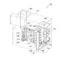
続いて、本実施形態にかかる基板処理装置が備える処理炉202及びその周辺の構成について、図2〜図4を参照しながら説明する。図2は、本発明の一実施形態にかかる基板処理装置が備える処理炉の概略構成図である。図3は、本発明の一実施形態にかかる基板処理装置が備えるガス供給系、バイパス配管、ガス排気系の概略構成図である。図4は、図3に示すバイパス配管、ガス排気系の他の構成例を示す概略構成図である。(3) Configuration of Processing Furnace Subsequently, the
(処理室)
図2に示すように、本実施形態にかかる処理炉202は、反応管としてのアウターチューブ205を有している。アウターチューブ205は、石英(SiO2)または炭化シリコン(SiC)等の耐熱材料からなり、上端が閉塞し下端が開口した円筒形状に形成されている。アウターチューブ205の内側の筒中空部には、減圧下で基板としてのウエハ200を処理する処理室201が形成されている。処理室201は、基板としてのウエハ200を、後述するボート130によって水平姿勢で垂直方向に多段に整列した状態で収容可能に構成されている。なお、本発明は、処理室201内に複数枚のウエハ200が収容される場合に限定されず、処理室201内に1枚のウエハ200が収容される場合であっても好適に適用可能である。(Processing room)
As shown in FIG. 2, the
アウターチューブ205の外側には、アウターチューブ205と同心円状に、加熱機構としてのヒータ206が設けられている。ヒータ206は円筒形状であり、ヒータ素線とその周囲に設けられた断熱部材とにより構成され、図示しない保持体に支持されることにより垂直に据え付けられている。なお、ヒータ206の近傍には、処理室201内の温度を検出する温度検出体としての温度センサ(図示せず)が設けられている。ヒータ206及び温度センサには、温度制御部302が電気的に接続されている。温度制御部302は、温度センサにより検出された温度情報に基づきヒータ206への通電具合を調節し、処理室201内の温度が所望のタイミングにて所望の温度分布となるよう制御する。 A
アウターチューブ205の下方には、アウターチューブ205と同心円状に、マニホールド209が配設されている。マニホールド209は、例えば、ステンレス等からなり、上端及び下端が開口した円筒形状に形成されている。このマニホールド209は、アウターチューブ205を支持するように設けられている。なお、マニホールド209とアウターチューブ205との間には、シール部材としてのOリングが設けられている。また、マニホールド209の下方には、予備室としてのロードロック室140が設けられている。ロードロック室140の天板251とマニホールド209との間には、シール部材としてのOリングが設けられている。このマニホールド209が天板251により支持されることにより、アウターチューブ205は垂直に据え付けられた状態となっている。このアウターチューブ205とマニホールド209とにより反応容器が形成される。なお、天板251には、処理炉202の開口部である炉口261が設けられている。 A manifold 209 is disposed below the
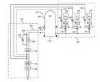
(ガス供給系)
図2に示すように、マニホールド209の側壁には、ウエハ200を処理する第1処理ガスを処理室201内へ供給する第1ガス供給系としての第1ガス供給管150と、ウエハ200を処理する第2処理ガスを処理室201内へ供給する第2ガス供給系としての第2ガス供給管160と、ウエハ200を処理する第3処理ガスを処理室201内へ供給する第3ガス供給系としての第3ガス供給管170とが合流するように一本化して接続され
ている。第1ガス供給管150、第2ガス供給管160、第3ガス供給管170が合流するように一本化した下流側には、処理室201内に処理ガスを供給するガス供給ノズル220が接続されている。ガス供給ノズル220は、処理室の内壁に沿うように鉛直方向に配設されている。ガス供給ノズルには、積層されたウエハ200間の空間に処理ガスを供給するように、図示しないガス供給孔がそれぞれ設けられている。また、ガス供給ノズルは、かかる形態に限定されず、高さの異なる複数の支流ノズルに下流側が分岐されていてもよく、かかる場合、各支流ノズルには上述のガス供給孔を設けられず、各支流ノズルの下流端部から上方へ向けて処理ガスが供給されることとしてもよい。(Gas supply system)
As shown in FIG. 2, on the side wall of the manifold 209, a first
第1ガス供給管150には、上流から順に、第1処理ガスを供給する第1処理ガス供給源153、流量制御手段としてのマスフローコントローラ(MFC)152、バルブ151が直列に設けられている。第2ガス供給管160には、上流から順に、第2処理ガスを供給する第2処理ガス供給源163、流量制御手段としてのマスフローコントローラ(MFC)162、バルブ161が直列に設けられている。第3ガス供給管170には、上流から順に、第3処理ガスを供給する第3処理ガス供給源173、流量制御手段としてのマスフローコントローラ(MFC)172、バルブ171が直列に設けられている。第1処理ガス供給源153は、第1処理ガスとして例えば可燃性ガスであるSiH4ガスやSi2H6ガス等のシラン系ガスやGeH4ガス等のゲルマン系ガスを供給するように構成され、第2処理ガス供給源163は第2処理ガスとして例えば支燃性ガスであるCl2ガスを供給するように構成され、第3処理ガス供給源173は第3処理ガスとして例えばH2ガスを供給するように構成されている。A first processing
なお、本発明にかかるガス供給系は、合流するように1本化されてマニホールド209の側面に接続される上述の場合に限らず、第1ガス供給管150、第2ガス供給管160、第3ガス供給管170がそれぞれ個別にマニホールド209の側面に接続されていてもよい。かかる場合には、第1ガス供給管150、第2ガス供給管160、第3ガス供給管170のそれぞれの下流側にガス供給ノズルが接続されることとなる。なお、ガス供給系の数は、上述のように3つである場合に限らず、基板処理の内容に応じて、4つ以上であってもよく、2つ以下であってもよい。 The gas supply system according to the present invention is not limited to the above-described case where the gas supply systems are merged and connected to the side surface of the manifold 209, but the first
(ガス排気系)
図2に示すように、マニホールド209の側壁には、処理室201内の雰囲気を排気するガス排気系としてのガス排気管231が接続されている。ガス排気管231には、少なくとも2つの真空ポンプが直列に設けられている。ガス排気管231を流れるガスの最上流側に位置する真空ポンプは、メカニカルブースタポンプであるように構成されている。(Gas exhaust system)
As shown in FIG. 2, a
具体的には図3に示すように、ガス排気管231には、APCバルブ232、真空ポンプとしての第1メカニカルブースタポンプ(ルーツポンプ)233、第2メカニカルブースタポンプ234、ドライポンプ235が、上流から順に直列に設けられている。 Specifically, as shown in FIG. 3, the
第1メカニカルブースタポンプ233及び第2メカニカルブースタポンプ234は、例えば、ケーシング内にある2個のマユ型ロータが、その軸端の駆動ギアにより互いに反対方向に同期回転するように構成されている。ケーシングの一端に設けられた吸気口からケーシング内部へと吸引されたガスは、2つのロータとケーシングとの間の空間に閉じ込められつつロータの回転により移動させられ、ケーシングの他端に設けられた排気口から排出されるように構成されている。ロータ同士およびロータとケーシングとの間は、わずかな隙間(例えば0.1mm〜0.3mm)を保って回転するように構成されており、ケーシング内には、潤滑油を必要としないように構成されている。したがってオイルフリーな真空排気が可能なように構成されている。 The first
ドライポンプ235は、処理室201内の汚染の原因となるポンプ油を使わない構成であれば、ルーツ型、クロー型、スクリュー型、ターボ型、スクロール型等のさまざまな方式による機械式真空ポンプ、あるいはソープションポンプ等の物理化学的な方式による真空ポンプを用いることが可能である。 The
ガス排気管231に、第1メカニカルブースタポンプ233、第2メカニカルブースタポンプ234、ドライポンプ235を直列に設けることにより、例えば6万slmの排気速度が実現されるように構成されている。なお、全体の排気速度は、主に第1メカニカルブースタポンプ233の排気性能により定まる。すなわち、第1メカニカルブースタポンプ233の排気速度が全体の排気速度を定める律速となり、主に第1メカニカルブースタポンプ233の排気性能により処理室201内の圧力が決定されるように構成されている。 By providing a first
ガス排気管231には、APCバルブ232の上流側と下流側(第1メカニカルブースタポンプ233とAPCバルブ232との間)とを結ぶように、スロー排気管236が設けられている。スロー排気管236には開閉バルブ237が設けられている。また、APCバルブ232の上流側におけるガス排気管231内には、図示しないが、処理室201内の圧力を検知する圧力検知手段としての圧力センサが設けられている。なお、圧力センサは、ガス排気管231内に限らず処理室201内に設けられていてもよい。圧力センサ及びAPCバルブ232には、圧力制御部304が電気的に接続されている。圧力制御部304は、圧力センサにより検出された圧力に基づいてAPCバルブ232の開度を調節し、処理室201内の圧力が所望のタイミングにて所望の圧力となるように制御するよう構成されている。 The
なお、本発明は、図3のように第1メカニカルブースタポンプ233、第2メカニカルブースタポンプ234、ドライポンプ235の3つの真空ポンプが設けられる場合に限定されない。すなわち、図4のように、第1メカニカルブースタポンプ233とドライポンプ235との2つの真空ポンプのみが設けられる場合(第2メカニカルブースタポンプ234が設けられていない場合)であっても好適に適用可能である。 In addition, this invention is not limited to when the three vacuum pumps of the 1st
(バイパス配管)
図3に示すように、本実施形態にかかる基板処理装置101は、第1ガス供給管150とガス排気管231とを処理室201を介さずに接続する第1バイパス配管155と、第2ガス供給管160とガス排気管231とを処理室201を介さずに接続する第2バイパス配管165と、第3ガス供給管170とガス排気管231とを処理室201を介さずに接続する第3バイパス配管175と、を備えている。(Bypass piping)
As shown in FIG. 3, the
第1バイパス配管155の上流側は、第1ガス供給管150のバルブ151とマスフローコントローラ152との間に接続されており、第2バイパス配管165の上流側は、第2ガス供給管160のバルブ161とマスフローコントローラ162との間に接続されており、第3バイパス配管175の上流側は、第3ガス供給管170のバルブ171とマスフローコントローラ172との間に接続されている。また、第1バイパス配管155、第2バイパス配管165、第3バイパス配管175の下流側は、ガス排気管231の第1メカニカルブースタポンプ233と、その下流に位置する真空ポンプ(図3の形態で有れば第2メカニカルブースタポンプ234、図4の形態で有ればドライポンプ235)と、の間に接続されている。第1バイパス配管155、第2バイパス配管165、第3バイパス配管175の下流側の構成が、本実施形態にかかる基板処理装置の特徴の一つである。 The upstream side of the
第1バイパス配管155、第2バイパス配管165、第3バイパス配管175には、それぞれバルブ156,166,176が設けられている。なお、第1バイパス配管155
、第2バイパス配管165、第3バイパス配管175を流れるガスの流量は、それぞれ例えば1slm程度である。
The flow rate of the gas flowing through the
なお、本実施形態においては、バイパス配管は全ての処理ガス源に対応する本数(つまり3本)が設けられることとしているが、本発明はかかる形態に限定されない。すなわち、一部の処理ガス源にのみ設けられることとしても本発明は適用可能である。例えば、第1ガス供給管150及び第2ガス供給管160の両方あるいはいずれか一方にバイパス配管が設けられ、その他のガス供給管にはバイパス配管が設けられなくてもよい。 In the present embodiment, the number of bypass pipes corresponding to all processing gas sources (that is, three) is provided, but the present invention is not limited to such a form. In other words, the present invention can be applied even when only some of the processing gas sources are provided. For example, bypass piping may be provided in both or one of the first
(ボートエレベータ)
ロードロック室140を構成する側壁の外面には、ボートエレベータ115が設けられている。ボートエレベータ115は、下基板245、ガイドシャフト264、ボール螺子244、上基板247、昇降モータ248、昇降基板252、及びベローズ265を備えている。下基板245は、ロードロック室140を構成する側壁の外面に水平姿勢で固定されている。下基板245には、昇降台249と嵌合するガイドシャフト264、及び昇降台249と螺合するボール螺子244がそれぞれ鉛直姿勢で設けられている。ガイドシャフト264及びボール螺子244の上端には、上基板247が水平姿勢で固定されている。ボール螺子244は、上基板247に設けられた昇降モータ248により回転させられるように構成されている。また、ガイドシャフト264は、昇降台249の上下動を許容しつつ水平方向の回転を抑制するように構成されている。そして、ボール螺子244を回転させることにより、昇降台249が昇降するように構成されている。(Boat elevator)
A
昇降台249には、中空の昇降シャフト250が垂直姿勢で固定されている。昇降台249と昇降シャフト250との連結部は、気密に構成されている。昇降シャフト250は、昇降台249と共に昇降するように構成されている。昇降シャフト250の下方側端部は、ロードロック室140を構成する天板251を貫通している。天板251に設けられる貫通穴の内径は、昇降シャフト250と天板251とが接触することのない様に、昇降シャフト250の外径よりも大きく構成されている。ロードロック室140と昇降台249との間には、昇降シャフト250の周囲を覆うように、伸縮性を有する中空伸縮体としてのベローズ265が設けられている。昇降台249とベローズ265との連結部、及び天板251とベローズ265との連結部はそれぞれ気密に構成されており、ロードロック室140内の気密が保持されるように構成されている。ベローズ265は、昇降台249の昇降量に対応できる充分な伸縮量を有している。ベローズ265の内径は、昇降シャフト250とベローズ265とが接触することのない様に、昇降シャフト250の外径よりも充分に大きく構成されている。 A
ロードロック室140内に突出した昇降シャフト250の下端には、昇降基板252が水平姿勢で固定されている。昇降シャフト250と昇降基板252との連結部は、気密に構成されている。昇降基板252の上面には、Oリング等のシール部材を介してシールキャップ219が気密に取付けられている。シールキャップ219は、例えばステンレス等の金属よりなり、円盤状に形成されている。昇降モータ248を駆動してボール螺子244を回転させ、昇降台249、昇降シャフト250、昇降基板252、及びシールキャップ219を上昇させることにより、処理炉202内にボート130が搬入(ボートローディング)されると共に、処理炉202の開口部である炉口261がシールキャップ219により閉塞されるよう構成されている。また、昇降モータ248を駆動してボール螺子244を回転させ、昇降台249、昇降シャフト250、昇降基板252、及びシールキャップ219を下降させることにより、処理室201内からボート130が搬出(ボートアンローディング)されるよう構成されている。昇降モータ248には、駆動制御部305が電気的に接続されている。駆動制御部305は、ボートエレベータ115が所望のタイミングにて所望の動作をするよう制御する。 An elevating
昇降基板252の下面には、Oリング等のシール部材を介して駆動部カバー253が気密に取付けられている。昇降基板252と駆動部カバー253とにより駆動部収納ケース256が構成されている。駆動部収納ケース256の内部は、ロードロック室140内の雰囲気と隔離されている。駆動部収納ケース256の内部には、回転機構254が設けられている。回転機構254には電力供給ケーブル258が接続されている。電力供給ケーブル258は、昇降シャフト250の上端から昇降シャフト250内を通って回転機構254まで導かれており、回転機構254に電力を供給するように構成されている。回転機構254が備える回転軸255の上端部は、シールキャップ219を貫通して、基板保持具としてのボート130を下方から支持するように構成されている。回転機構254を作動させることにより、ボート130に保持されたウエハ200を処理室201内で回転させることが可能なように構成されている。回転機構254には、駆動制御部305が電気的に接続されている。駆動制御部305は、回転機構254が所望のタイミングにて所望の動作をするよう制御する。 A
また、駆動部収納ケース256の内部であって回転機構254の周囲には、冷却機構257が設けられている。冷却機構257及びシールキャップ219には冷却流路259が形成されている。冷却流路259には冷却水を供給する冷却水配管260が接続されている。冷却水配管260は、昇降シャフト250の上端から昇降シャフト250内を通って冷却流路259まで導かれ、冷却流路259にそれぞれ冷却水を供給するように構成されている。 In addition, a
(ボート)
基板保持具としてのボート130は、例えば石英(SiO2)や炭化珪素(SiC)等の耐熱性材料からなり、複数枚のウエハ200を水平姿勢でかつ互いに中心を揃えた状態で整列させて多段に保持するように構成されている。なお、ボート130の下部には、例えば石英や炭化珪素等の耐熱性材料からなる円板形状をした断熱部材としての断熱板216が、水平姿勢で多段に複数枚配置されている。断熱板216は、ヒータ206からの熱をマニホールド209側に伝えにくくするように機能する。(boat)
The
(コントローラ)
また、本実施形態にかかる基板処理装置は、制御手段としてのコントローラ300を有している。コントローラ300は、CPU、メモリ、HDDなどの記憶装置、操作部、入出力部を備えた主制御部301を備えている。主制御部301は、上述の温度制御部302、ガス流量制御部303、圧力制御部304、駆動制御部305、ボートエレベータ115の昇降モータ248、及び回転機構254に電気的に接続されており、基板処理装置全体を制御するように構成されている。(controller)
Further, the substrate processing apparatus according to the present embodiment has a
(4)基板処理工程
以下に、本実施形態にかかる半導体装置の製造工程の一工程として、ウエハ200上にエピタキシャルシリコン膜(Epi−Si膜)をサイクル成長させる基板処理工程について、図9を参照しながら説明する。図9は、本発明の一実施形態にかかる基板処理工程のフロー図である。なお、基板処理装置101を構成する各部の動作は、コントローラ300により制御される。なお、第1処理ガス供給源153、第2処理ガス供給源163、及び第3処理ガス供給源173には、第1処理ガスとしての可燃性ガスであるSiH4ガス、第2処理ガスとしての支燃性ガスであるCl2ガス、及び第3処理ガスとしてのH2ガスがそれぞれ封入されていることとする。また、処理対象のウエハ200の表面のすくなくとも一部には、シリコンが露出しているものとする。(4) Substrate Processing Step A substrate processing step for cyclically growing an epitaxial silicon film (Epi-Si film) on the
(基板搬入工程(S10))
まず、ウエハ移載機112により、降下状態のボート130に複数枚の処理対象のウエハ200を装填する。所定枚数のウエハ200の装填が完了したら、昇降モータ248を駆動して、所定枚数のウエハ200を保持したボート130を処理室201内に搬入(ボートローディング)すると共に、処理炉202の開口部である炉口261をシールキャップ219により閉塞する。(Substrate carrying-in process (S10))
First, a plurality of
(減圧・昇温工程(S20))
次に、処理室201内が所望の圧力(真空度)となるように、第1メカニカルブースタポンプ233、第2メカニカルブースタポンプ234、ドライポンプ235により処理室201内を真空排気する。この際、バルブ151,156,161,166,171,176は閉めておく。(Decompression / Temperature raising step (S20))
Next, the
そして、処理室201内の圧力を圧力センサにより測定し、この測定した圧力に基づきAPCバルブ232をフィードバック制御する。本実施形態においては、処理室201内は例えば40Pa以下に減圧される。また、第1メカニカルブースタポンプ233と第2メカニカルブースタポンプ234との間のガス排気管231内は、例えば100Pa程度に減圧される。なお、第1バイパス配管155のバルブ156の下流側、第2バイパス配管165のバルブ166の下流側、第3バイパス配管175のバルブ176の下流側も、第1メカニカルブースタポンプ233と第2メカニカルブースタポンプ234との間のガス排気管231内と連通していることから、同様に例えば100Pa程度に減圧される。 Then, the pressure in the
なお、ガス排気管231に設けられた第1メカニカルブースタポンプ233、第2メカニカルブースタポンプ234、ドライポンプ235は、いずれもポンプ油を用いない構成であることから、処理室201内、ガス排気管231、第1バイパス配管155内、第2バイパス配管165内、第3バイパス配管175内はクリーン(オールフリー)に保たれる。 Note that the first
また、処理室201内が所望の温度分布となるように、ヒータ206により処理室201内を加熱する。この際、温度センサにより温度を検出し、検出した温度情報に基づきヒータ206への通電具合をフィードバック制御する。続いて、回転機構254により、ボート130及びウエハ200を回転させる。 Further, the inside of the
(SiH4ガス供給工程(S30))
次に、第1処理ガスとしてのSiH4ガスを、第1処理ガス供給源153(第1ガス供給管150)より処理室201内へと供給する。具体的には、バルブ156を閉めたままバルブ151を開け、マスフローコントローラ152により流量制御しながら、処理室201内へのSiH4ガスの供給を開始する。処理室201内に供給されたSiH4ガスは、ウエハ200表面と接触した後、ガス排気管231から処理室201外へと排気される。SiH4ガスの供給を所定時間継続した後、バルブ151を閉め、処理室201内へのSiH4ガスの供給を停止する。(SiH4 gas supply step (S30))
Next, SiH4 gas as the first processing gas is supplied into the
なお、SiH4ガス供給工程(S30)においては、バルブ176を閉めたままバルブ171を開け、マスフローコントローラ172により流量制御しながら、SiH4ガスと同時にH2ガスを処理室201内へ供給することが好ましい。これにより、薄膜成長させる下地の表面等に存在する酸素(O)元素を還元させ、Epi−Si膜中の酸素濃度を低下させることができる。In the SiH4 gas supply step (S30), the
(Cl2ガスバイパス排出工程(S31))
SiH4ガス供給工程(S30)の実施が完了するまで、Cl2ガスバイパス排出工程(S31)を並行して実施し、第2処理ガス供給源163(第2ガス供給管160)から
のCl2ガスの流量を安定させておく。Cl2ガスバイパス排出工程(S31)では、第2バイパス配管165にCl2ガスを流してガス排気管231に排気しておく。すなわち、バルブ161を閉めたままバルブ166を開け、Cl2ガスを処理室201内に供給することなく第2バイパス配管165からガス排気管231へと排気することにより、第2処理ガス供給源163(第2ガス供給管160)からのCl2ガスの供給流量が供給開始直後に一時的に過大になってしまうオーバーシュート現象を収束させておく。(Cl2 gas bypass discharge step (S31))
SiH4 to implementation of the gas supply step (S30) is completed, and carried out in parallel with Cl2 gas bypass discharging step (S31), Cl2 from the second processing gas supply source 163 (second gas supply pipe 160) Keep the gas flow stable. In the Cl2 gas bypass discharge step (S 31), Cl2 gas is allowed to flow through the
なお、上述したように、第1メカニカルブースタポンプ233と第2メカニカルブースタポンプ234との間のガス排気管231内は例えば100Pa程度に減圧され、処理室201内の圧力は例えば40Pa以下に減圧されている。すなわち、Cl2ガスが排出されるガス排気管231内の圧力の方が、処理室201内の圧力の方よりも高いことになる。このような圧力状態であっても、本実施形態では、第2バイパス配管165の下流側は第1メカニカルブースタポンプ233と第2メカニカルブースタポンプ234との間に接続されているため、処理室201内へCl2ガスが逆拡散(逆流)してしまうことが抑制される。すなわち、ガス排気管231の第2バイパス配管165との接続箇所の上流側には、第1メカニカルブースタポンプ233が設けられているため、第2バイパス配管165からガス排気管231へと排気されたCl2ガスが、ガス排気管231の下流側へ流れずに上流側(処理室201側)へと逆拡散(逆流)してしまうことが抑制される。As described above, the inside of the
(Cl2ガス供給工程(S40))
第2処理ガス供給源163(第2ガス供給管160)からのCl2ガスの流量が安定したら、第2ガス供給管160より処理室201内へとCl2ガスを供給する。具体的には、バルブ166を閉め、バルブ161を開け、マスフローコントローラ162により流量制御しながら、処理室201内へのCl2ガスの供給を開始する。処理室201内に供給されたCl2ガスは、ウエハ200表面と接触した後、ガス排気管231から処理室201外へと排気される。(Cl2 gas supply step (S40))
When the flow rate of Cl2 gas from the second processing gas supply source 163 (second gas supply pipe 160) is stabilized, the Cl2 gas is supplied from the second
なお、Cl2ガスバイパス排出工程(S31)における第2ガス供給管160からのCl2ガスの供給先(第2バイパス配管165内)は例えば100Pa程度に減圧されており、Cl2ガス供給工程(S40)における第2ガス供給管160からのCl2ガスの供給先(処理室201内)は例えば40Pa以下に減圧されている。すなわち、Cl2ガスバイパス排出工程(S31)とCl2ガス供給工程(S40)とでは、Cl2ガスの供給先に若干の圧力差が存在することとなる。しかしながら、この程度の圧力差は、基板処理の品質や歩留まりにほとんど影響しない。つまり、バイパス排出工程(S31)からCl2ガス供給工程(S40)へと切り替えたとしても、第2ガス供給管160からのCl2ガスの供給流量の乱れは少なく、基板処理の品質や歩留まりにほとんど影響しない。Note that the supply destination of Cl2 gas from the second gas supply pipe 160 (in the second bypass pipe 165) in the Cl2 gas bypass discharge step (S31) is reduced to, for example, about 100 Pa, and the Cl2 gas supply step ( The supply destination of the Cl2 gas from the second gas supply pipe 160 (in the processing chamber 201) in S40) is reduced to 40 Pa or less, for example. That is, in the Cl2 gas bypass discharge step (S31) and the Cl2 gas supply step (S40), there is a slight pressure difference at the Cl2 gas supply destination. However, such a pressure difference hardly affects the quality and yield of substrate processing. In other words, even when the bypass discharge process (S31) is switched to the Cl2 gas supply process (S40), the supply flow rate of the Cl2 gas from the second
なお、Cl2ガス供給工程(S40)においては、バルブ176を閉めたままバルブ171を開け、マスフローコントローラ172により流量制御しながら、Cl2ガスと同時にH2ガスを処理室201内へ供給することが好ましい。これにより、薄膜成長させる下地の表面等に存在する酸素(O)元素を還元させ、Epi−Si膜中の酸素濃度を低下させることができる。In the Cl2 gas supply step (S40), the
このように、SiH4ガス供給工程(S30)とCl2ガス供給工程(S40)とを実施してウエハ200の表面にSiH4ガスとCl2ガスとを供給することにより、ウエハ200上のシリコン露出面上にEpi−Si膜を選択的に成長させることができる。As described above, the SiH4 gas supply step (S 30) and the Cl2 gas supply step (S 40) are performed to supply SiH4 gas and Cl2 gas to the surface of the
(Cl2ガスバイパス排出工程(S51))
Cl2ガス供給工程(S40)を所定時間(例えば30秒)実施したら、バルブ161を閉め、バルブ166を開け、Cl2ガスを処理室201内に供給することなく第2バイ
パス配管165からガス排気管231へと排気する。かかる場合においても、第2バイパス配管165の下流側は、第1メカニカルブースタポンプ233と第2メカニカルブースタポンプ234との間に接続されているため、処理室201内へCl2ガスが逆拡散(逆流)してしまうことが抑制される。(Cl2 gas bypass discharge step (S51))
When the Cl2 gas supply step (S40) is performed for a predetermined time (for example, 30 seconds), the
なお、Cl2ガスバイパス排出工程(S51)においては、バルブ166を閉めたままバルブ161を閉めることとし、第2バイパス配管165へCl2ガスを流すことなくCl2ガスの処理室201内への供給を停止してもよい。かかる場合であっても、後工程でCl2ガスバイパス排出工程(S31)を再び実施することにより、処理室201内へ供給するCl2ガスの供給流量を安定させることができる。In the Cl2 gas bypass discharging step (S51), and closing the
(H2ガス供給工程(S50))
Cl2ガスバイパス排出工程(S51)と並行して、H2ガス供給工程(S50)を実施する。すなわち、具体的には、バルブ176を閉め、バルブ171を開け、マスフローコントローラ162により流量制御しながら、処理室201内へのH2ガスの供給を開始する。これによりウエハ200やEpi−Si膜の表面に存在する酸素(O)元素を還元させ、Epi−Si膜中の酸素濃度を低下させることができる。H2ガスの供給を所定時間継続した後、バルブ176を閉め、処理室201内へのH2ガスの供給を停止する。(H2 gas supply step (S50))
In parallel with the Cl2 gas bypass discharge step (S51), the H2 gas supply step (S50) is performed. Specifically, the
(繰り返し工程)
以下、SiH4ガス供給工程(S30)〜H2ガスバイパス排出工程(S51)を1サイクルとして、このサイクルを繰り返すことにより、ウエハ200上のシリコン露出面上に所望の厚さのEpi−Si膜を選択的に成長させる。なお、本発明は上述の実施形態に限定されず、SiH4ガス供給工程(S30)、Cl2ガス供給工程(S40)、H2ガス供給工程(S50)を同時に行うこととしてもよい。かかる場合であっても、Cl2ガス供給工程(S40)の実施前後には、Cl2ガスバイパス排出工程(S31)とCl2ガスバイパス排出工程(S51)とをそれぞれ実施する。また、H2ガス供給工程(S50)は必ずしも実施しなくてもよく、SiH4ガス供給工程(S30)〜H2ガスバイパス排出工程(S51)を1サイクルとして、このサイクルを繰り返すこととしてもよい。(Repeated process)
Hereinafter, the SiH4 gas supply process (S30) to the H2 gas bypass discharge process (S51) are set as one cycle, and this cycle is repeated, whereby an Epi-Si film having a desired thickness is formed on the silicon exposed surface on the
(処理ガス排気工程(S60))
所望の厚さのEpi−Si膜を成長させてウエハ200を処理した後、ガス排気管231を介して処理室201内に残留している処理ガスを排気する。この際、バルブ151,161,171は閉めたままとする。なお、図示しない不活性ガス供給ラインからN2ガス等の不活性ガスを処理室201内に供給することにより、処理室201内からの処理ガスの排気を促すことができる。処理室201内から処理ガスを排気した後、処理室201内に不活性ガスを供給しつつAPCバルブ232の開度を調整させ、処理室201内の圧力を大気圧にまで復帰させる。続いて、回転機構254の動作を停止させる。なお、APCバルブ232を閉める場合には、開閉バルブ237を開けて、スロー排気管236により処理室201内を低速で排気することとしてもよい。(Processing gas exhaust process (S60))
After the Epi-Si film having a desired thickness is grown and the
(基板搬出工程(S70))
その後、昇降モータ248を作動させてシールキャップ219を下降させ、処理炉202の開口部である炉口261を開口させると共に、成膜済のウエハ200を保持したボート130を処理室201外へと搬出(ボートアンローディング)する。その後、ウエハ移載機112により、処理済のウエハ200をボート130より取り出し(ウエハディスチャージ)て、本実施形態にかかる基板処理工程を完了する。(Substrate unloading step (S70))
Thereafter, the
なお、ウエハ200を処理する際の処理条件としては、例えば、Epi−Si膜の成膜において、処理温度400℃〜700℃、処理圧力1Pa〜200Paが例示される。ま
た、SiH4ガス供給工程(S30)においては、SiH4ガスの供給流量:100sccm、H2ガスの供給流量:1slmが例示され、Cl2ガス供給工程(S40)においては、Cl2ガスの供給流量:50sccm、H2ガスの供給流量:1slmが例示される。Examples of processing conditions for processing the
(5)効果
本実施形態によれば、以下に示す(a)〜(e)のうち1つまたは複数の効果を奏する。(5) Effect According to the present embodiment, one or more of the following effects (a) to (e) are achieved.
(a)本実施形態によれば、SiH4ガス供給工程(S30)と並行してCl2ガスバイパス排出工程(S31)を実施する。Cl2ガスバイパス排出工程(S31)では、バルブ161を閉めたままバルブ166を開け、Cl2ガスを処理室201内に供給することなく第2バイパス配管165からガス排気管231へと排気することにより、第2処理ガス供給源163(第2ガス供給管160)からのCl2ガスの供給流量が供給開始直後に一時的に過大になってしまうオーバーシュート現象を収束させておく。これにより、Cl2ガスバイパス排出工程(S31)の後に実施するCl2ガス供給工程(S40)において、処理室201内に供給するCl2ガスの供給流量を安定させることができ、基板処理の品質を向上させ、歩留りを改善させることができる。(A) According to the present embodiment, the Cl2 gas bypass discharge step (S31) is performed in parallel with the SiH4 gas supply step (S30). In the Cl2 gas bypass discharge step (S31), the
(b)本実施形態によれば、第2バイパス配管165の下流側は、第1メカニカルブースタポンプ233と第2メカニカルブースタポンプ234との間に接続されている。このため、処理室201内へCl2ガスが逆拡散(逆流)してしまうことを抑制できる。例えば、Cl2ガスバイパス排出工程(S31)やCl2ガスバイパス排出工程(S51)においては、第1メカニカルブースタポンプ233と第2メカニカルブースタポンプ234との間のガス排気管231内は例えば100Pa程度に減圧され、処理室201内の圧力は例えば40Pa以下に減圧されている。すなわち、Cl2ガスが排出されるガス排気管231内の圧力の方が、処理室201内の圧力の方よりも高いことになる。このような圧力状態であっても、本実施形態では、ガス排気管231の第2バイパス配管165との接続箇所の上流側に第1メカニカルブースタポンプ233が設けられているため、第2バイパス配管165からガス排気管231へと排気されたCl2ガスが、ガス排気管231の下流側へ流れずに上流側(処理室201側)へと逆拡散(逆流)してしまうことを抑制できる。その結果、ガス排気管231内に残留していた異物等がCl2ガスと共に処理室201内に侵入してしまうことが抑制され、基板処理の品質を向上させ、歩留りを改善させることができる。(B) According to the present embodiment, the downstream side of the
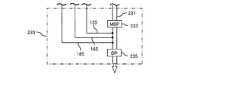
参考までに、従来の基板処理装置が備えるガス供給系、バイパス配管、ガス排気系の概略構成を図5及び図6に示す。図5に示す従来の基板処理装置では、ガス排気管231に第1メカニカルブースタポンプ233、第2メカニカルブースタポンプ234、ドライポンプ235の3つの真空ポンプが直列に設けられており、図6に示す従来の基板処理装置では、ガス排気管231に第1メカニカルブースタポンプ233、ドライポンプ235の2つの真空ポンプが直列に設けられている。いずれの場合においても、第1バイパス配管155、第2バイパス配管165、第3バイパス配管175の下流側は、ガス排気管231の第1メカニカルブースタポンプ233の上流側に接続されている。発明者等の鋭意研究によれば、かかる構成では、Cl2ガスを第2バイパス配管165から排気させようとすると、ガス排気管231へと排気されたCl2ガスが処理室201内へ逆拡散(逆流)してしまう場合がある。すなわち、従来の基板処理装置では、ガス排気管231の第2バイパス配管165との接続箇所の上流側には本実施形態のように真空ポンプ(第1メカニカルブースタポンプ233)が設けられていないため、Cl2ガスが排出されるガス排気管231内の圧力の方が処理室201内の圧力の方よりも高い(あるいは同程度である)と、ガス排気管231へと排気されたCl2ガスが処理室201内へ逆拡散(逆流)して
しまう場合がある。For reference, schematic configurations of a gas supply system, a bypass pipe, and a gas exhaust system included in a conventional substrate processing apparatus are shown in FIGS. In the conventional substrate processing apparatus shown in FIG. 5, three vacuum pumps of a first
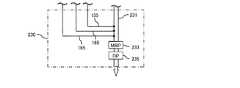
(c)本実施形態によれば、第1バイパス配管155、第2バイパス配管165、第3バイパス配管175の下流側を、ガス排気管231の第1メカニカルブースタポンプ233と、その下流に位置する真空ポンプ(図3の形態で有れば第2メカニカルブースタポンプ234、図4の形態で有ればドライポンプ235)と、の間に接続することとにより、Cl2ガスの処理室201内への逆拡散(逆流)を抑制できる。すなわち、第1バイパス配管155、第2バイパス配管165、第3バイパス配管175の下流側に専用の真空ポンプを新たに設ける必要がない。そのため、基板処理装置101の構成を単純化させることができ、基板処理装置101のコストや設置スペース(フットプリント)の増大を抑制することができる。(C) According to the present embodiment, the downstream side of the
参考までに、バイパス配管に専用ポンプを設けた従来の基板処理装置が備えるガス供給系、バイパス配管、ガス排気系の概略構成を図7及び図8に示す。図7に示す従来の基板処理装置では、ガス排気管231に第1メカニカルブースタポンプ233、第2メカニカルブースタポンプ234、ドライポンプ235の3つの真空ポンプが直列に設けられており、図8に示す従来の基板処理装置では、ガス排気管231に第1メカニカルブースタポンプ233、ドライポンプ235の2つの真空ポンプが直列に設けられている。いずれの場合においても、第1バイパス配管155、第2バイパス配管165、第3バイパス配管175はガス排気管231に接続されておらず、また、第1バイパス配管155、第2バイパス配管165、第3バイパス配管175の下流側には専用ポンプ238が新たに設けられている。発明者等の鋭意検討によれば、かかる構成では、基板処理装置101の構成が複雑化し、基板処理装置101のコストや設置スペース(フットプリント)が増大してしまう場合がある。 For reference, FIGS. 7 and 8 show schematic configurations of a gas supply system, a bypass pipe, and a gas exhaust system provided in a conventional substrate processing apparatus in which a dedicated pump is provided in the bypass pipe. In the conventional substrate processing apparatus shown in FIG. 7, three vacuum pumps of a first
(d)本実施形態によれば、ガス排気管231に設けられた第1メカニカルブースタポンプ233、第2メカニカルブースタポンプ234、ドライポンプ235は、いずれもポンプ油を用いない構成であることから、処理室201内、ガス排気管231内、第1バイパス配管155内、第2バイパス配管165内、第3バイパス配管175内をクリーンに保つ(オールフリーに保つ)ことが可能となる。(D) According to the present embodiment, the first
(e)本実施形態によれば、ガス排気管231には、真空ポンプとして、ターボ分子ポンプ(TMP)ではなく、メカニカルブースタポンプ(MBP)とドライポンプ(DP)とを設けることとしている。ターボ分子ポンプとは、機械式真空ポンプの一種であり、金属製のタービン翼を持った回転体であるロータを高速回転させ、ガス分子を弾き飛ばす(ガス分子を押しやり圧縮する)ことにより排気するポンプである。ターボ分子ポンプでは大気圧まで圧縮することは困難であるため、ターボ分子ポンプの後に他の粗引きポンプを下流側に接続して使用する必要がある。発明者等の鋭意検討によれば、1度に多数枚の基板を処理するバッチ式基板処理(バッチ式エピタキシャル膜成長)においては、処理室201内に大流量の処理ガスを供給する必要があるため、有効作動領域が狭く大流量の処理ガスを排気することが困難なターボ分子ポンプよりも、有効作動領域が広く大流量の処理ガスを排気することが容易なメカニカルブースタポンプとドライポンプとの組み合わせの方が好適であるものと考えられる。また、ガス排気管231とのメタルシールやボルト締めによる固定が必要なターボ分子ポンプ(TMP)よりも、メカニカルブースタポンプやドライポンプの方が容易に設置できるものと考えられる。一般的には、ターボ分子ポンプは、メカニカルブースタポンプと比較して有効作動領域が狭い場合が多いため、仮にガス排気管231にターボ分子ポンプ(TMP)を設ける場合には、ガス排気管231の最上流側(処理室201に最も近い位置)に設けることで、ターボ分子ポンプ(TMP)の排気効率を最適化させ、処理室201内への処理ガスの逆拡散(逆流)を抑制するようにしなければならない。(E) According to the present embodiment, the
<本発明の他の実施形態>
上述の実施形態において、バルブ151とバルブ156、バルブ161とバルブ166、バルブ171とバルブ176は、それぞれインターロックとして構成してもよい。例えば、バルブ151とバルブ156のうちいずれかの一方のバルブを閉める場合には、他方のバルブを自動的に開放するように構成し、バルブ151とバルブ156のうちいずれか一方のバルブを開ける場合には、他方のバルブを自動的に閉めるように構成してもよい。かかる開閉動作はコントローラ300により自動的に制御される。このように構成することにより、バルブの開閉操作の誤りによる処理ガスの供給流量の乱れを抑制でき、基板処理の品質を向上させ、歩留りを改善させることができる。<Other Embodiments of the Present Invention>
In the above-described embodiment, the
上述の実施形態では、Cl2ガスの供給流量を安定させるようにCl2ガスについてのみ第2バイパス配管165を用いて排気する例について説明したが、本発明はかかる構成に限定されない。すなわち、SiH4ガスについても、Cl2ガスの場合と同様に、第1バイパス配管155を用いて供給流量を安定させてもよい。また、H2ガスについても、Cl2ガスの場合と同様に、第3バイパス配管175を用いて供給流量を安定させてもよい。In the above embodiment, an example has been described in which evacuated with the
上述の実施形態では、処理室201内にSiH4ガス、Cl2ガス、H2ガスを供給してEpi−Si膜を成長させる場合について説明したが、本発明はかかる実施形態に限定されない。すなわち、第1処理ガス供給源153にSi2H6ガス等のSiH4ガス以外のシラン系ガスが封入されており、処理室201内にかかるSi2H6ガス等のシラン系ガス、Cl2ガス、H2ガスを順次あるいは同時に供給することによりEpi−Si膜を成長させる場合にも、本発明は好適に適用可能である。In the above-described embodiment, the case where the Epi-Si film is grown by supplying SiH4 gas, Cl2 gas, and H2 gas into the
また、第1処理ガス供給源153、第2処理ガス供給源163、及び第3処理ガス供給源173に、SiH4ガスやSi2H6ガス等のシラン系ガス、GeH4ガス等のゲルマン系ガス、及びCl2ガスがそれぞれ封入されており、処理室201内にこれら各種ガスを順次あるいは同時に供給することによりEpi−SiGe膜を成長させる場合にも、本発明は好適に適用可能である。このとき、第1バイパス配管155、第2バイパス配管165、第3バイパス配管175を用い上述の実施形態と同様にSiとGeの比率を調整して各種ガスの流量を安定させることが可能であるとともに、各種ガスの処理室201内への逆拡散(逆流)を抑制することが可能である。又、Bドープを行う場合も、B含有ガスを供給する前にバイパス配管を用い、上述の実施形態と同様にB含有ガスの流量を安定させることが可能である。In addition, the first processing
<本発明の好ましい態様>
以下に、本発明の好ましい態様を付記する。<Preferred embodiment of the present invention>
Hereinafter, preferred embodiments of the present invention will be additionally described.
本発明の第1の態様によれば、
基板を収容する処理室と、
前記基板を処理する処理ガスを処理ガス源から前記処理室内へ供給するガス供給系と、
前記処理室内の雰囲気を排気するガス排気系と、
前記ガス排気系に直列に設けられた少なくとも2つの真空ポンプと、
前記ガス供給系と前記ガス排気系とを前記処理室を介さずに接続するバイパス配管と、を含み、
前記真空ポンプの内、前記ガス排気系を流れるガスの最上流側に位置する真空ポンプはメカニカルブースタポンプであって、前記バイパス配管は、前記メカニカルブースタポンプとその下流に位置する真空ポンプとの間の位置に接続される基板処理装置が提供される。According to a first aspect of the invention,
A processing chamber for accommodating the substrate;
A gas supply system for supplying a processing gas for processing the substrate from a processing gas source into the processing chamber;
A gas exhaust system for exhausting the atmosphere in the processing chamber;
At least two vacuum pumps provided in series with the gas exhaust system;
A bypass pipe for connecting the gas supply system and the gas exhaust system without going through the processing chamber,
Among the vacuum pumps, the vacuum pump located on the most upstream side of the gas flowing through the gas exhaust system is a mechanical booster pump, and the bypass pipe is between the mechanical booster pump and a vacuum pump located downstream thereof. A substrate processing apparatus connected to the position is provided.
本発明の第2の態様によれば、
前記ガス排気系の前記バイパス配管との接続部よりもガスの下流側の真空ポンプは、ドライポンプである第1の態様に記載の基板処理装置が提供される。According to a second aspect of the invention,
The substrate processing apparatus according to the first aspect, in which the vacuum pump on the downstream side of the gas from the connection portion of the gas exhaust system with the bypass pipe is a dry pump.
本発明の第3の態様によれば、
前記ガス排気系の前記バイパス配管との接続部よりもガスの下流側の真空ポンプは、メカニカルブースタポンプである第1の態様に記載の基板処理装置が提供される。According to a third aspect of the invention,
The substrate processing apparatus according to the first aspect, in which the vacuum pump on the downstream side of the gas from the connection portion of the gas exhaust system with the bypass pipe is a mechanical booster pump.
本発明の第4の態様によれば、
前記ガス排気系の前記バイパス配管との接続部よりもガス下流側の真空ポンプは、上流側から順にメカニカルブースタポンプとドライポンプである第1の態様に記載の基板処理装置が提供される。According to a fourth aspect of the invention,
The substrate processing apparatus according to the first aspect, in which the vacuum pump on the gas downstream side of the connection portion with the bypass pipe of the gas exhaust system is a mechanical booster pump and a dry pump in order from the upstream side.
本発明の第5の態様によれば、
前記処理ガス源が複数設けられ、前記バイパス配管は前記処理ガス源に対応する数を有し、それぞれの前記バイパス配管が前記メカニカルブースタポンプとその下流に位置する真空ポンプとの間の位置に接続される第1の態様に記載の基板処理装置が提供される。According to a fifth aspect of the present invention,
A plurality of the processing gas sources are provided, and the bypass pipes have a number corresponding to the processing gas sources, and each of the bypass pipes is connected to a position between the mechanical booster pump and a vacuum pump located downstream thereof. A substrate processing apparatus according to the first aspect is provided.
本発明の第6の態様によれば、
前記処理室は複数の基板を収容する請求項1に記載の基板処理装置が提供される。According to a sixth aspect of the present invention,
The substrate processing apparatus according to claim 1, wherein the processing chamber accommodates a plurality of substrates.
本発明の第7の態様によれば、
基板を処理するガスを供給するガス供給系と、
基板を処理する処理室と、
前記供給系より供給されたガスを排気するガス排気系と、
前記ガス供給系と前記ガス排気系を直接接続するバイパス配管と、を含み、
前記ガス排気系にメカニカルブースタポンプとドライポンプを設け、前記バイパス配管は前記メカニカルブースタポンプと前記ドライポンプとの間に接続される基板処理装置が提供される。According to a seventh aspect of the present invention,
A gas supply system for supplying a gas for processing the substrate;
A processing chamber for processing the substrate;
A gas exhaust system for exhausting the gas supplied from the supply system;
A bypass pipe that directly connects the gas supply system and the gas exhaust system,
A substrate processing apparatus is provided in which a mechanical booster pump and a dry pump are provided in the gas exhaust system, and the bypass pipe is connected between the mechanical booster pump and the dry pump.
本発明の第8の態様によれば、
基板を処理するガスを供給するガス供給系と、
基板を処理する処理室と、
前記供給系より供給されたガスを排気するガス排気系と、
前記ガス供給系と前記ガス排気系を直接接続するバイパス配管と、を含み、
前記ガス排気系にターボ分子ポンプを含まない3つの真空ポンプを設け、前記バイパス配管はガスの最上流側に位置する真空ポンプと他の真空ポンプとの間に接続される基板処理装置が提供される。According to an eighth aspect of the present invention,
A gas supply system for supplying a gas for processing the substrate;
A processing chamber for processing the substrate;
A gas exhaust system for exhausting the gas supplied from the supply system;
A bypass pipe that directly connects the gas supply system and the gas exhaust system,
There is provided a substrate processing apparatus in which three vacuum pumps not including a turbo molecular pump are provided in the gas exhaust system, and the bypass pipe is connected between a vacuum pump located on the most upstream side of the gas and another vacuum pump. The
本発明の第9の態様によれば、
前記3つのポンプは、2つのメカニカルブースタポンプと1つのドライポンプであって、前記最上流側の真空ポンプはメカニカルブースタポンプである第8の態様に記載の基板処理装置が提供される。According to a ninth aspect of the present invention,
The substrate processing apparatus according to an eighth aspect, wherein the three pumps are two mechanical booster pumps and one dry pump, and the most upstream vacuum pump is a mechanical booster pump.
本発明の第10の態様によれば、
基板を収容する処理室と、前記基板を処理する処理ガスを処理ガス源から前記処理室内へ供給するガス供給系と、前記処理室内の雰囲気を排気するガス排気系と、前記ガス排気系に直列に設けられた少なくとも2つの真空ポンプと、前記ガス供給系と前記ガス排気系とを前記処理室を介さずに接続するバイパス配管と、を含み、前記真空ポンプの内、前記
ガス排気系を流れるガスの最上流側に位置する真空ポンプはメカニカルブースタポンプであって、前記バイパス配管は、前記メカニカルブースタポンプとその下流に位置する真空ポンプとの間の位置に接続される基板処理装置により実施され、
前記基板を処理する前に前記処理ガス源からの前記処理ガスの流量を安定させるよう前記バイパス配管に前記処理ガスを流して前記ガス排気系に排気する工程と、
前記処理室内に前記処理ガス源から前記処理ガスを供給して前記基板を処理する工程と、
前記基板を処理した後、前記ガス排気系を介して前記処理室内の前記処理ガスを排気する工程と、
を有する半導体装置の製造方法が提供される。According to a tenth aspect of the present invention,
A processing chamber for containing a substrate, a gas supply system for supplying a processing gas for processing the substrate from a processing gas source to the processing chamber, a gas exhaust system for exhausting an atmosphere in the processing chamber, and a series of the gas exhaust system And a bypass pipe connecting the gas supply system and the gas exhaust system without going through the processing chamber, and flows through the gas exhaust system in the vacuum pump. The vacuum pump located on the most upstream side of the gas is a mechanical booster pump, and the bypass pipe is implemented by a substrate processing apparatus connected to a position between the mechanical booster pump and a vacuum pump located downstream thereof. ,
Flowing the process gas through the bypass pipe and exhausting it to the gas exhaust system so as to stabilize the flow rate of the process gas from the process gas source before processing the substrate;
Supplying the processing gas from the processing gas source into the processing chamber to process the substrate;
Exhausting the processing gas in the processing chamber through the gas exhaust system after processing the substrate;
A method of manufacturing a semiconductor device having the above is provided.
101 基板処理装置
150 第1ガス供給管(ガス供給系)
153 第1処理ガス供給源
155 第1バイパス配管
160 第2ガス供給管(ガス供給系)
163 第2処理ガス供給源
165 第2バイパス配管
170 第3ガス供給管(ガス供給系)
173 第3処理ガス供給源
175 第3バイパス配管
200 ウエハ(基板)
201 処理室
202 処理炉
231 ガス排気管(排気系)
233 第1メカニカルブースタポンプ(真空ポンプ)
234 第2メカニカルブースタポンプ(真空ポンプ)
235 ドライポンプ(真空ポンプ)
300 コントローラ101
153 First processing
163 Second process
173 Third processing
201
233 First mechanical booster pump (vacuum pump)
234 Second mechanical booster pump (vacuum pump)
235 Dry pump (vacuum pump)
300 controller
Claims (5)
Translated fromJapanese前記基板を処理する処理ガスを処理ガス源から前記処理室内へ供給するガス供給系と、
前記処理室内の雰囲気を排気するガス排気系と、
前記ガス排気系に直列に設けられた少なくとも3つの真空ポンプと、
前記ガス供給系と前記ガス排気系とを前記処理室を介さずに接続するバイパス配管と、を含み、
前記3つの真空ポンプは、上流側から順に、それぞれ第1メカニカルブースタポンプ、第2メカニカルブースタポンプ、ドライポンプとして構成され、
前記バイパス配管は、前記第1メカニカルブースタポンプとその下流に位置する前記第2メカニカルブースタポンプとの間の位置に接続される基板処理装置。A processing chamber for accommodating the substrate;
A gas supply system for supplying a processing gas for processing the substrate from a processing gas source into the processing chamber;
A gas exhaust system for exhausting the atmosphere in the processing chamber;
At leastthree vacuum pumps provided in series with the gas exhaust system;
A bypass pipe for connecting the gas supply system and the gas exhaust system without going through the processing chamber,
Thethree vacuum pumpsare configured as a first mechanical booster pump, a second mechanical booster pump, and a dry pump, respectively, in order from the upstream side.
The bypass pipe is a substrate processing apparatus connected to a position betweenthe first mechanical booster pump and the second mechanical booster pump located downstream thereof .
前記基板を処理する処理ガスを処理ガス源から前記処理室内へ供給するガス供給系と、
前記処理室内の雰囲気を排気するガス排気系と、
前記ガス排気系に直列に設けられた少なくとも3つの真空ポンプと、
前記ガス供給系と前記ガス排気系とを前記処理室を介さずに接続するバイパス配管と、
前記ガス供給系と前記ガス排気系とを制御する制御部と、
を含み、
前記3つの真空ポンプは、上流側から順に、それぞれ第1メカニカルブースタポンプ、第2メカニカルブースタポンプ、ドライポンプとして構成されており、
前記バイパス配管は、前記第1メカニカルブースタポンプとその下流に位置する前記第2メカニカルブースタポンプとの間の位置に接続され、
前記制御部は、
前記処理ガス源からの処理ガスの流量を安定させるように前記基板を処理する前に前記バイパス配管に処理ガスを流して前記ガス排気系に排気させた後、
前記処理室内に前記処理ガス源から前記処理ガスを供給して前記基板を処理し、
前記基板を処理した後、前記ガス排気系を介して前記処理室内の前記処理ガスを排気させるように、前記ガス供給系と前記ガス排気系とを制御する基板処理装置。A processing chamber for accommodating the substrate;
A gas supply system for supplying a processing gas for processing the substrate from a processing gas source into the processing chamber;
A gas exhaust system for exhausting the atmosphere in the processing chamber;
At least three vacuum pumps provided in series with the gas exhaust system;
A bypass pipe connecting the gas supply system and the gas exhaust system without going through the processing chamber;
A control unit for controlling the gas supply system and the gas exhaust system;
Including
The three vacuum pumps are configured as a first mechanical booster pump, a second mechanical booster pump, and a dry pump, respectively, in order from the upstream side.
The bypass pipe is connected to a position between the first mechanical booster pump and the second mechanical booster pump located downstream thereof,
The controller is
After processing the substrate so as to stabilize the flow rate of the processing gas from the processing gas source, the processing gas is allowed to flow through the bypass pipe and exhausted to the gas exhaust system.
Supplying the processing gas from the processing gas source into the processing chamber to process the substrate;
A substrate processing apparatusthat controls the gas supply system and the gas exhaust system so that the processing gas in the processing chamber is exhausted through the gas exhaust system after the substrate is processed.
し、それぞれの前記バイパス配管が前記第1メカニカルブースタポンプと前記第2メカニカルブースタポンプとの間の位置に接続される請求項1又は2に記載の基板処理装置。A plurality of the processing gas sources are provided, the bypass pipes have a number corresponding to the processing gas sources, and each of the bypass pipes is ata positionbetweenthe first mechanical booster pump andthe second mechanical booster pump. The substrate processing apparatus ofClaim 1 or 2 connected.
前記処理ガス源からの処理ガスの流量を安定させるように前記基板を処理する前に前記バイパス配管に処理ガスを流して前記ガス排気系に排気する工程と、
前記処理室内に前記処理ガス源から前記処理ガスを供給して前記基板を処理する工程と、
前記基板を処理した後、前記ガス排気系を介して前記処理室内の前記処理ガスを排気する工程と、
を有する半導体装置の製造方法。A processing chamber for containing a substrate, a gas supply system for supplying a processing gas for processing the substrate from a processing gas source to the processing chamber, a gas exhaust system for exhausting an atmosphere in the processing chamber, and a series of the gas exhaust system At least three vacuum pumps, and a bypass pipe connecting the gas supply system and the gas exhaust system without going through the processing chamber, the three vacuum pumps in order from the upstream side, Each of them is configured as a first mechanical booster pump, a second mechanical booster pump, and a dry pump, and the bypass pipe is connected to a position between the first mechanical booster pump and the second mechanical booster pump located downstream thereof. Implemented by a substrate processing apparatus,
Before the substrate is processed so as to stabilize the flow rate of the processing gas from the processing gas source, a processing gas is flowed through the bypass pipe and exhausted to the gas exhaust system;
Supplying the processing gas from the processing gas source into the processing chamber to process the substrate;
Exhausting the processing gas in the processing chamber through the gas exhaust system after processing the substrate;
A method for manufacturing a semiconductor device comprising:
前記処理ガス源からの処理ガスの流量を安定させるように前記基板を処理する前に前記バイパス配管に処理ガスを流して前記ガス排気系に排気する工程と、Before the substrate is processed so as to stabilize the flow rate of the processing gas from the processing gas source, a processing gas is flowed through the bypass pipe and exhausted to the gas exhaust system;
前記処理室内に前記処理ガス源から前記処理ガスを供給して前記基板を処理する工程と、Supplying the processing gas from the processing gas source into the processing chamber to process the substrate;
前記基板を処理した後、前記ガス排気系を介して前記処理室内の前記処理ガスを排気する工程と、Exhausting the processing gas in the processing chamber through the gas exhaust system after processing the substrate;
を有する基板処理方法。A substrate processing method.
Priority Applications (3)
| Application Number | Priority Date | Filing Date | Title |
|---|---|---|---|
| JP2008232618AJP5226438B2 (en) | 2008-09-10 | 2008-09-10 | Substrate processing apparatus, semiconductor device manufacturing method, and substrate processing method |
| US12/553,143US20100058984A1 (en) | 2008-09-10 | 2009-09-03 | Substrate Processing Apparatus |
| KR1020090084962AKR101073571B1 (en) | 2008-09-10 | 2009-09-09 | Substrate processing apparatus |
Applications Claiming Priority (1)
| Application Number | Priority Date | Filing Date | Title |
|---|---|---|---|
| JP2008232618AJP5226438B2 (en) | 2008-09-10 | 2008-09-10 | Substrate processing apparatus, semiconductor device manufacturing method, and substrate processing method |
Publications (2)
| Publication Number | Publication Date |
|---|---|
| JP2010067788A JP2010067788A (en) | 2010-03-25 |
| JP5226438B2true JP5226438B2 (en) | 2013-07-03 |
Family
ID=41798127
Family Applications (1)
| Application Number | Title | Priority Date | Filing Date |
|---|---|---|---|
| JP2008232618AExpired - Fee RelatedJP5226438B2 (en) | 2008-09-10 | 2008-09-10 | Substrate processing apparatus, semiconductor device manufacturing method, and substrate processing method |
Country Status (3)
| Country | Link |
|---|---|
| US (1) | US20100058984A1 (en) |
| JP (1) | JP5226438B2 (en) |
| KR (1) | KR101073571B1 (en) |
Families Citing this family (367)
| Publication number | Priority date | Publication date | Assignee | Title |
|---|---|---|---|---|
| US10378106B2 (en) | 2008-11-14 | 2019-08-13 | Asm Ip Holding B.V. | Method of forming insulation film by modified PEALD |
| US9394608B2 (en) | 2009-04-06 | 2016-07-19 | Asm America, Inc. | Semiconductor processing reactor and components thereof |
| US8802201B2 (en) | 2009-08-14 | 2014-08-12 | Asm America, Inc. | Systems and methods for thin-film deposition of metal oxides using excited nitrogen-oxygen species |
| JP5304749B2 (en)* | 2010-08-05 | 2013-10-02 | 株式会社島津製作所 | Vacuum analyzer |
| US9312155B2 (en) | 2011-06-06 | 2016-04-12 | Asm Japan K.K. | High-throughput semiconductor-processing apparatus equipped with multiple dual-chamber modules |
| US10364496B2 (en) | 2011-06-27 | 2019-07-30 | Asm Ip Holding B.V. | Dual section module having shared and unshared mass flow controllers |
| US10854498B2 (en) | 2011-07-15 | 2020-12-01 | Asm Ip Holding B.V. | Wafer-supporting device and method for producing same |
| US20130023129A1 (en)* | 2011-07-20 | 2013-01-24 | Asm America, Inc. | Pressure transmitter for a semiconductor processing environment |
| US9017481B1 (en) | 2011-10-28 | 2015-04-28 | Asm America, Inc. | Process feed management for semiconductor substrate processing |
| KR101427726B1 (en)* | 2011-12-27 | 2014-08-07 | 가부시키가이샤 히다치 고쿠사이 덴키 | Substrate processing apparatus and method of manufacturing semiconductor device |
| JP5937385B2 (en)* | 2012-03-16 | 2016-06-22 | 東京エレクトロン株式会社 | Gas supply method, gas supply system and semiconductor manufacturing apparatus for semiconductor manufacturing apparatus |
| US9659799B2 (en) | 2012-08-28 | 2017-05-23 | Asm Ip Holding B.V. | Systems and methods for dynamic semiconductor process scheduling |
| US9021985B2 (en) | 2012-09-12 | 2015-05-05 | Asm Ip Holdings B.V. | Process gas management for an inductively-coupled plasma deposition reactor |
| US10714315B2 (en) | 2012-10-12 | 2020-07-14 | Asm Ip Holdings B.V. | Semiconductor reaction chamber showerhead |
| US20160376700A1 (en) | 2013-02-01 | 2016-12-29 | Asm Ip Holding B.V. | System for treatment of deposition reactor |
| US9484191B2 (en) | 2013-03-08 | 2016-11-01 | Asm Ip Holding B.V. | Pulsed remote plasma method and system |
| US9589770B2 (en) | 2013-03-08 | 2017-03-07 | Asm Ip Holding B.V. | Method and systems for in-situ formation of intermediate reactive species |
| US9240412B2 (en) | 2013-09-27 | 2016-01-19 | Asm Ip Holding B.V. | Semiconductor structure and device and methods of forming same using selective epitaxial process |
| US10683571B2 (en) | 2014-02-25 | 2020-06-16 | Asm Ip Holding B.V. | Gas supply manifold and method of supplying gases to chamber using same |
| US10167557B2 (en) | 2014-03-18 | 2019-01-01 | Asm Ip Holding B.V. | Gas distribution system, reactor including the system, and methods of using the same |
| US11015245B2 (en) | 2014-03-19 | 2021-05-25 | Asm Ip Holding B.V. | Gas-phase reactor and system having exhaust plenum and components thereof |
| US10858737B2 (en) | 2014-07-28 | 2020-12-08 | Asm Ip Holding B.V. | Showerhead assembly and components thereof |
| US9890456B2 (en) | 2014-08-21 | 2018-02-13 | Asm Ip Holding B.V. | Method and system for in situ formation of gas-phase compounds |
| US9657845B2 (en) | 2014-10-07 | 2017-05-23 | Asm Ip Holding B.V. | Variable conductance gas distribution apparatus and method |
| US10941490B2 (en) | 2014-10-07 | 2021-03-09 | Asm Ip Holding B.V. | Multiple temperature range susceptor, assembly, reactor and system including the susceptor, and methods of using the same |
| KR102300403B1 (en) | 2014-11-19 | 2021-09-09 | 에이에스엠 아이피 홀딩 비.브이. | Method of depositing thin film |
| KR102263121B1 (en) | 2014-12-22 | 2021-06-09 | 에이에스엠 아이피 홀딩 비.브이. | Semiconductor device and manufacuring method thereof |
| US10529542B2 (en) | 2015-03-11 | 2020-01-07 | Asm Ip Holdings B.V. | Cross-flow reactor and method |
| US10276355B2 (en) | 2015-03-12 | 2019-04-30 | Asm Ip Holding B.V. | Multi-zone reactor, system including the reactor, and method of using the same |
| US10458018B2 (en) | 2015-06-26 | 2019-10-29 | Asm Ip Holding B.V. | Structures including metal carbide material, devices including the structures, and methods of forming same |
| US10600673B2 (en) | 2015-07-07 | 2020-03-24 | Asm Ip Holding B.V. | Magnetic susceptor to baseplate seal |
| US10043661B2 (en) | 2015-07-13 | 2018-08-07 | Asm Ip Holding B.V. | Method for protecting layer by forming hydrocarbon-based extremely thin film |
| US10083836B2 (en) | 2015-07-24 | 2018-09-25 | Asm Ip Holding B.V. | Formation of boron-doped titanium metal films with high work function |
| JP6560924B2 (en)* | 2015-07-29 | 2019-08-14 | 株式会社Kokusai Electric | Substrate processing apparatus, semiconductor device manufacturing method, and program |
| US9960072B2 (en) | 2015-09-29 | 2018-05-01 | Asm Ip Holding B.V. | Variable adjustment for precise matching of multiple chamber cavity housings |
| US10211308B2 (en) | 2015-10-21 | 2019-02-19 | Asm Ip Holding B.V. | NbMC layers |
| US10322384B2 (en) | 2015-11-09 | 2019-06-18 | Asm Ip Holding B.V. | Counter flow mixer for process chamber |
| US11139308B2 (en) | 2015-12-29 | 2021-10-05 | Asm Ip Holding B.V. | Atomic layer deposition of III-V compounds to form V-NAND devices |
| US10468251B2 (en) | 2016-02-19 | 2019-11-05 | Asm Ip Holding B.V. | Method for forming spacers using silicon nitride film for spacer-defined multiple patterning |
| US10529554B2 (en) | 2016-02-19 | 2020-01-07 | Asm Ip Holding B.V. | Method for forming silicon nitride film selectively on sidewalls or flat surfaces of trenches |
| US10501866B2 (en) | 2016-03-09 | 2019-12-10 | Asm Ip Holding B.V. | Gas distribution apparatus for improved film uniformity in an epitaxial system |
| US10343920B2 (en) | 2016-03-18 | 2019-07-09 | Asm Ip Holding B.V. | Aligned carbon nanotubes |
| US9892913B2 (en) | 2016-03-24 | 2018-02-13 | Asm Ip Holding B.V. | Radial and thickness control via biased multi-port injection settings |
| US10865475B2 (en) | 2016-04-21 | 2020-12-15 | Asm Ip Holding B.V. | Deposition of metal borides and silicides |
| US10190213B2 (en) | 2016-04-21 | 2019-01-29 | Asm Ip Holding B.V. | Deposition of metal borides |
| US10087522B2 (en) | 2016-04-21 | 2018-10-02 | Asm Ip Holding B.V. | Deposition of metal borides |
| US10032628B2 (en) | 2016-05-02 | 2018-07-24 | Asm Ip Holding B.V. | Source/drain performance through conformal solid state doping |
| US10367080B2 (en) | 2016-05-02 | 2019-07-30 | Asm Ip Holding B.V. | Method of forming a germanium oxynitride film |
| KR102592471B1 (en) | 2016-05-17 | 2023-10-20 | 에이에스엠 아이피 홀딩 비.브이. | Method of forming metal interconnection and method of fabricating semiconductor device using the same |
| US11453943B2 (en) | 2016-05-25 | 2022-09-27 | Asm Ip Holding B.V. | Method for forming carbon-containing silicon/metal oxide or nitride film by ALD using silicon precursor and hydrocarbon precursor |
| US10388509B2 (en) | 2016-06-28 | 2019-08-20 | Asm Ip Holding B.V. | Formation of epitaxial layers via dislocation filtering |
| US10612137B2 (en) | 2016-07-08 | 2020-04-07 | Asm Ip Holdings B.V. | Organic reactants for atomic layer deposition |
| US9859151B1 (en) | 2016-07-08 | 2018-01-02 | Asm Ip Holding B.V. | Selective film deposition method to form air gaps |
| US9793135B1 (en) | 2016-07-14 | 2017-10-17 | ASM IP Holding B.V | Method of cyclic dry etching using etchant film |
| US10714385B2 (en) | 2016-07-19 | 2020-07-14 | Asm Ip Holding B.V. | Selective deposition of tungsten |
| KR102354490B1 (en) | 2016-07-27 | 2022-01-21 | 에이에스엠 아이피 홀딩 비.브이. | Method of processing a substrate |
| US10177025B2 (en) | 2016-07-28 | 2019-01-08 | Asm Ip Holding B.V. | Method and apparatus for filling a gap |
| US10395919B2 (en) | 2016-07-28 | 2019-08-27 | Asm Ip Holding B.V. | Method and apparatus for filling a gap |
| KR102532607B1 (en) | 2016-07-28 | 2023-05-15 | 에이에스엠 아이피 홀딩 비.브이. | Substrate processing apparatus and method of operating the same |
| US9887082B1 (en) | 2016-07-28 | 2018-02-06 | Asm Ip Holding B.V. | Method and apparatus for filling a gap |
| US9812320B1 (en) | 2016-07-28 | 2017-11-07 | Asm Ip Holding B.V. | Method and apparatus for filling a gap |
| US10090316B2 (en) | 2016-09-01 | 2018-10-02 | Asm Ip Holding B.V. | 3D stacked multilayer semiconductor memory using doped select transistor channel |
| US10410943B2 (en) | 2016-10-13 | 2019-09-10 | Asm Ip Holding B.V. | Method for passivating a surface of a semiconductor and related systems |
| US10643826B2 (en) | 2016-10-26 | 2020-05-05 | Asm Ip Holdings B.V. | Methods for thermally calibrating reaction chambers |
| US11532757B2 (en) | 2016-10-27 | 2022-12-20 | Asm Ip Holding B.V. | Deposition of charge trapping layers |
| US10714350B2 (en) | 2016-11-01 | 2020-07-14 | ASM IP Holdings, B.V. | Methods for forming a transition metal niobium nitride film on a substrate by atomic layer deposition and related semiconductor device structures |
| US10229833B2 (en) | 2016-11-01 | 2019-03-12 | Asm Ip Holding B.V. | Methods for forming a transition metal nitride film on a substrate by atomic layer deposition and related semiconductor device structures |
| US10435790B2 (en) | 2016-11-01 | 2019-10-08 | Asm Ip Holding B.V. | Method of subatmospheric plasma-enhanced ALD using capacitively coupled electrodes with narrow gap |
| US10643904B2 (en) | 2016-11-01 | 2020-05-05 | Asm Ip Holdings B.V. | Methods for forming a semiconductor device and related semiconductor device structures |
| US10134757B2 (en) | 2016-11-07 | 2018-11-20 | Asm Ip Holding B.V. | Method of processing a substrate and a device manufactured by using the method |
| KR102546317B1 (en) | 2016-11-15 | 2023-06-21 | 에이에스엠 아이피 홀딩 비.브이. | Gas supply unit and substrate processing apparatus including the same |
| US10340135B2 (en) | 2016-11-28 | 2019-07-02 | Asm Ip Holding B.V. | Method of topologically restricted plasma-enhanced cyclic deposition of silicon or metal nitride |
| KR102762543B1 (en) | 2016-12-14 | 2025-02-05 | 에이에스엠 아이피 홀딩 비.브이. | Substrate processing apparatus |
| US11447861B2 (en) | 2016-12-15 | 2022-09-20 | Asm Ip Holding B.V. | Sequential infiltration synthesis apparatus and a method of forming a patterned structure |
| US11581186B2 (en) | 2016-12-15 | 2023-02-14 | Asm Ip Holding B.V. | Sequential infiltration synthesis apparatus |
| US9916980B1 (en) | 2016-12-15 | 2018-03-13 | Asm Ip Holding B.V. | Method of forming a structure on a substrate |
| KR102700194B1 (en) | 2016-12-19 | 2024-08-28 | 에이에스엠 아이피 홀딩 비.브이. | Substrate processing apparatus |
| US10269558B2 (en) | 2016-12-22 | 2019-04-23 | Asm Ip Holding B.V. | Method of forming a structure on a substrate |
| US10867788B2 (en) | 2016-12-28 | 2020-12-15 | Asm Ip Holding B.V. | Method of forming a structure on a substrate |
| US11390950B2 (en) | 2017-01-10 | 2022-07-19 | Asm Ip Holding B.V. | Reactor system and method to reduce residue buildup during a film deposition process |
| US10655221B2 (en) | 2017-02-09 | 2020-05-19 | Asm Ip Holding B.V. | Method for depositing oxide film by thermal ALD and PEALD |
| US10468261B2 (en) | 2017-02-15 | 2019-11-05 | Asm Ip Holding B.V. | Methods for forming a metallic film on a substrate by cyclical deposition and related semiconductor device structures |
| US10283353B2 (en) | 2017-03-29 | 2019-05-07 | Asm Ip Holding B.V. | Method of reforming insulating film deposited on substrate with recess pattern |
| US10529563B2 (en) | 2017-03-29 | 2020-01-07 | Asm Ip Holdings B.V. | Method for forming doped metal oxide films on a substrate by cyclical deposition and related semiconductor device structures |
| US10103040B1 (en) | 2017-03-31 | 2018-10-16 | Asm Ip Holding B.V. | Apparatus and method for manufacturing a semiconductor device |
| USD830981S1 (en) | 2017-04-07 | 2018-10-16 | Asm Ip Holding B.V. | Susceptor for semiconductor substrate processing apparatus |
| KR102457289B1 (en) | 2017-04-25 | 2022-10-21 | 에이에스엠 아이피 홀딩 비.브이. | Method for depositing a thin film and manufacturing a semiconductor device |
| US10770286B2 (en) | 2017-05-08 | 2020-09-08 | Asm Ip Holdings B.V. | Methods for selectively forming a silicon nitride film on a substrate and related semiconductor device structures |
| US10892156B2 (en) | 2017-05-08 | 2021-01-12 | Asm Ip Holding B.V. | Methods for forming a silicon nitride film on a substrate and related semiconductor device structures |
| US10446393B2 (en) | 2017-05-08 | 2019-10-15 | Asm Ip Holding B.V. | Methods for forming silicon-containing epitaxial layers and related semiconductor device structures |
| US10504742B2 (en) | 2017-05-31 | 2019-12-10 | Asm Ip Holding B.V. | Method of atomic layer etching using hydrogen plasma |
| US10886123B2 (en) | 2017-06-02 | 2021-01-05 | Asm Ip Holding B.V. | Methods for forming low temperature semiconductor layers and related semiconductor device structures |
| US12040200B2 (en) | 2017-06-20 | 2024-07-16 | Asm Ip Holding B.V. | Semiconductor processing apparatus and methods for calibrating a semiconductor processing apparatus |
| US11306395B2 (en) | 2017-06-28 | 2022-04-19 | Asm Ip Holding B.V. | Methods for depositing a transition metal nitride film on a substrate by atomic layer deposition and related deposition apparatus |
| US10685834B2 (en) | 2017-07-05 | 2020-06-16 | Asm Ip Holdings B.V. | Methods for forming a silicon germanium tin layer and related semiconductor device structures |
| KR20190009245A (en) | 2017-07-18 | 2019-01-28 | 에이에스엠 아이피 홀딩 비.브이. | Methods for forming a semiconductor device structure and related semiconductor device structures |
| US11018002B2 (en) | 2017-07-19 | 2021-05-25 | Asm Ip Holding B.V. | Method for selectively depositing a Group IV semiconductor and related semiconductor device structures |
| US10541333B2 (en) | 2017-07-19 | 2020-01-21 | Asm Ip Holding B.V. | Method for depositing a group IV semiconductor and related semiconductor device structures |
| US11374112B2 (en) | 2017-07-19 | 2022-06-28 | Asm Ip Holding B.V. | Method for depositing a group IV semiconductor and related semiconductor device structures |
| US10605530B2 (en) | 2017-07-26 | 2020-03-31 | Asm Ip Holding B.V. | Assembly of a liner and a flange for a vertical furnace as well as the liner and the vertical furnace |
| US10312055B2 (en) | 2017-07-26 | 2019-06-04 | Asm Ip Holding B.V. | Method of depositing film by PEALD using negative bias |
| US10590535B2 (en) | 2017-07-26 | 2020-03-17 | Asm Ip Holdings B.V. | Chemical treatment, deposition and/or infiltration apparatus and method for using the same |
| TWI815813B (en) | 2017-08-04 | 2023-09-21 | 荷蘭商Asm智慧財產控股公司 | Showerhead assembly for distributing a gas within a reaction chamber |
| US10692741B2 (en) | 2017-08-08 | 2020-06-23 | Asm Ip Holdings B.V. | Radiation shield |
| US10770336B2 (en) | 2017-08-08 | 2020-09-08 | Asm Ip Holding B.V. | Substrate lift mechanism and reactor including same |
| US10249524B2 (en) | 2017-08-09 | 2019-04-02 | Asm Ip Holding B.V. | Cassette holder assembly for a substrate cassette and holding member for use in such assembly |
| US11769682B2 (en) | 2017-08-09 | 2023-09-26 | Asm Ip Holding B.V. | Storage apparatus for storing cassettes for substrates and processing apparatus equipped therewith |
| US11139191B2 (en) | 2017-08-09 | 2021-10-05 | Asm Ip Holding B.V. | Storage apparatus for storing cassettes for substrates and processing apparatus equipped therewith |
| US10236177B1 (en) | 2017-08-22 | 2019-03-19 | ASM IP Holding B.V.. | Methods for depositing a doped germanium tin semiconductor and related semiconductor device structures |
| USD900036S1 (en) | 2017-08-24 | 2020-10-27 | Asm Ip Holding B.V. | Heater electrical connector and adapter |
| US11830730B2 (en) | 2017-08-29 | 2023-11-28 | Asm Ip Holding B.V. | Layer forming method and apparatus |
| US11295980B2 (en) | 2017-08-30 | 2022-04-05 | Asm Ip Holding B.V. | Methods for depositing a molybdenum metal film over a dielectric surface of a substrate by a cyclical deposition process and related semiconductor device structures |
| US11056344B2 (en) | 2017-08-30 | 2021-07-06 | Asm Ip Holding B.V. | Layer forming method |
| KR102491945B1 (en) | 2017-08-30 | 2023-01-26 | 에이에스엠 아이피 홀딩 비.브이. | Substrate processing apparatus |
| KR102401446B1 (en) | 2017-08-31 | 2022-05-24 | 에이에스엠 아이피 홀딩 비.브이. | Substrate processing apparatus |
| US10607895B2 (en) | 2017-09-18 | 2020-03-31 | Asm Ip Holdings B.V. | Method for forming a semiconductor device structure comprising a gate fill metal |
| KR102630301B1 (en) | 2017-09-21 | 2024-01-29 | 에이에스엠 아이피 홀딩 비.브이. | Method of sequential infiltration synthesis treatment of infiltrateable material and structures and devices formed using same |
| US10844484B2 (en) | 2017-09-22 | 2020-11-24 | Asm Ip Holding B.V. | Apparatus for dispensing a vapor phase reactant to a reaction chamber and related methods |
| US10658205B2 (en) | 2017-09-28 | 2020-05-19 | Asm Ip Holdings B.V. | Chemical dispensing apparatus and methods for dispensing a chemical to a reaction chamber |
| US10403504B2 (en) | 2017-10-05 | 2019-09-03 | Asm Ip Holding B.V. | Method for selectively depositing a metallic film on a substrate |
| US10319588B2 (en) | 2017-10-10 | 2019-06-11 | Asm Ip Holding B.V. | Method for depositing a metal chalcogenide on a substrate by cyclical deposition |
| US10923344B2 (en) | 2017-10-30 | 2021-02-16 | Asm Ip Holding B.V. | Methods for forming a semiconductor structure and related semiconductor structures |
| KR102443047B1 (en) | 2017-11-16 | 2022-09-14 | 에이에스엠 아이피 홀딩 비.브이. | Method of processing a substrate and a device manufactured by the same |
| US10910262B2 (en) | 2017-11-16 | 2021-02-02 | Asm Ip Holding B.V. | Method of selectively depositing a capping layer structure on a semiconductor device structure |
| US11022879B2 (en) | 2017-11-24 | 2021-06-01 | Asm Ip Holding B.V. | Method of forming an enhanced unexposed photoresist layer |
| WO2019103613A1 (en) | 2017-11-27 | 2019-05-31 | Asm Ip Holding B.V. | A storage device for storing wafer cassettes for use with a batch furnace |
| CN111344522B (en) | 2017-11-27 | 2022-04-12 | 阿斯莫Ip控股公司 | Including clean mini-environment device |
| US10290508B1 (en) | 2017-12-05 | 2019-05-14 | Asm Ip Holding B.V. | Method for forming vertical spacers for spacer-defined patterning |
| US10872771B2 (en) | 2018-01-16 | 2020-12-22 | Asm Ip Holding B. V. | Method for depositing a material film on a substrate within a reaction chamber by a cyclical deposition process and related device structures |
| KR102695659B1 (en) | 2018-01-19 | 2024-08-14 | 에이에스엠 아이피 홀딩 비.브이. | Method for depositing a gap filling layer by plasma assisted deposition |
| TWI799494B (en) | 2018-01-19 | 2023-04-21 | 荷蘭商Asm 智慧財產控股公司 | Deposition method |
| USD903477S1 (en) | 2018-01-24 | 2020-12-01 | Asm Ip Holdings B.V. | Metal clamp |
| US11018047B2 (en) | 2018-01-25 | 2021-05-25 | Asm Ip Holding B.V. | Hybrid lift pin |
| USD880437S1 (en) | 2018-02-01 | 2020-04-07 | Asm Ip Holding B.V. | Gas supply plate for semiconductor manufacturing apparatus |
| US10535516B2 (en) | 2018-02-01 | 2020-01-14 | Asm Ip Holdings B.V. | Method for depositing a semiconductor structure on a surface of a substrate and related semiconductor structures |
| US11081345B2 (en) | 2018-02-06 | 2021-08-03 | Asm Ip Holding B.V. | Method of post-deposition treatment for silicon oxide film |
| US10896820B2 (en) | 2018-02-14 | 2021-01-19 | Asm Ip Holding B.V. | Method for depositing a ruthenium-containing film on a substrate by a cyclical deposition process |
| WO2019158960A1 (en) | 2018-02-14 | 2019-08-22 | Asm Ip Holding B.V. | A method for depositing a ruthenium-containing film on a substrate by a cyclical deposition process |
| US10731249B2 (en) | 2018-02-15 | 2020-08-04 | Asm Ip Holding B.V. | Method of forming a transition metal containing film on a substrate by a cyclical deposition process, a method for supplying a transition metal halide compound to a reaction chamber, and related vapor deposition apparatus |
| KR102636427B1 (en) | 2018-02-20 | 2024-02-13 | 에이에스엠 아이피 홀딩 비.브이. | Substrate processing method and apparatus |
| US10658181B2 (en) | 2018-02-20 | 2020-05-19 | Asm Ip Holding B.V. | Method of spacer-defined direct patterning in semiconductor fabrication |
| US10975470B2 (en) | 2018-02-23 | 2021-04-13 | Asm Ip Holding B.V. | Apparatus for detecting or monitoring for a chemical precursor in a high temperature environment |
| US11473195B2 (en) | 2018-03-01 | 2022-10-18 | Asm Ip Holding B.V. | Semiconductor processing apparatus and a method for processing a substrate |
| CN111712904B (en)* | 2018-03-06 | 2023-11-28 | 株式会社国际电气 | Processing device, exhaust system, semiconductor device manufacturing method |
| US11629406B2 (en) | 2018-03-09 | 2023-04-18 | Asm Ip Holding B.V. | Semiconductor processing apparatus comprising one or more pyrometers for measuring a temperature of a substrate during transfer of the substrate |
| US11114283B2 (en) | 2018-03-16 | 2021-09-07 | Asm Ip Holding B.V. | Reactor, system including the reactor, and methods of manufacturing and using same |
| KR102646467B1 (en) | 2018-03-27 | 2024-03-11 | 에이에스엠 아이피 홀딩 비.브이. | Method of forming an electrode on a substrate and a semiconductor device structure including an electrode |
| US11230766B2 (en) | 2018-03-29 | 2022-01-25 | Asm Ip Holding B.V. | Substrate processing apparatus and method |
| US10510536B2 (en) | 2018-03-29 | 2019-12-17 | Asm Ip Holding B.V. | Method of depositing a co-doped polysilicon film on a surface of a substrate within a reaction chamber |
| US11088002B2 (en) | 2018-03-29 | 2021-08-10 | Asm Ip Holding B.V. | Substrate rack and a substrate processing system and method |
| KR102501472B1 (en) | 2018-03-30 | 2023-02-20 | 에이에스엠 아이피 홀딩 비.브이. | Substrate processing method |
| KR102600229B1 (en) | 2018-04-09 | 2023-11-10 | 에이에스엠 아이피 홀딩 비.브이. | Substrate supporting device, substrate processing apparatus including the same and substrate processing method |
| TWI811348B (en) | 2018-05-08 | 2023-08-11 | 荷蘭商Asm 智慧財產控股公司 | Methods for depositing an oxide film on a substrate by a cyclical deposition process and related device structures |
| US12025484B2 (en) | 2018-05-08 | 2024-07-02 | Asm Ip Holding B.V. | Thin film forming method |
| US12272527B2 (en) | 2018-05-09 | 2025-04-08 | Asm Ip Holding B.V. | Apparatus for use with hydrogen radicals and method of using same |
| KR20190129718A (en) | 2018-05-11 | 2019-11-20 | 에이에스엠 아이피 홀딩 비.브이. | Methods for forming a doped metal carbide film on a substrate and related semiconductor device structures |
| KR102596988B1 (en) | 2018-05-28 | 2023-10-31 | 에이에스엠 아이피 홀딩 비.브이. | Method of processing a substrate and a device manufactured by the same |
| TWI840362B (en) | 2018-06-04 | 2024-05-01 | 荷蘭商Asm Ip私人控股有限公司 | Wafer handling chamber with moisture reduction |
| US11718913B2 (en) | 2018-06-04 | 2023-08-08 | Asm Ip Holding B.V. | Gas distribution system and reactor system including same |
| US11286562B2 (en) | 2018-06-08 | 2022-03-29 | Asm Ip Holding B.V. | Gas-phase chemical reactor and method of using same |
| US10797133B2 (en) | 2018-06-21 | 2020-10-06 | Asm Ip Holding B.V. | Method for depositing a phosphorus doped silicon arsenide film and related semiconductor device structures |
| KR102568797B1 (en) | 2018-06-21 | 2023-08-21 | 에이에스엠 아이피 홀딩 비.브이. | Substrate processing system |
| KR102854019B1 (en) | 2018-06-27 | 2025-09-02 | 에이에스엠 아이피 홀딩 비.브이. | Periodic deposition method for forming a metal-containing material and films and structures comprising the metal-containing material |
| TWI873894B (en) | 2018-06-27 | 2025-02-21 | 荷蘭商Asm Ip私人控股有限公司 | Cyclic deposition methods for forming metal-containing material and films and structures including the metal-containing material |
| KR102686758B1 (en) | 2018-06-29 | 2024-07-18 | 에이에스엠 아이피 홀딩 비.브이. | Method for depositing a thin film and manufacturing a semiconductor device |
| US10612136B2 (en) | 2018-06-29 | 2020-04-07 | ASM IP Holding, B.V. | Temperature-controlled flange and reactor system including same |
| US10755922B2 (en) | 2018-07-03 | 2020-08-25 | Asm Ip Holding B.V. | Method for depositing silicon-free carbon-containing film as gap-fill layer by pulse plasma-assisted deposition |
| US10388513B1 (en) | 2018-07-03 | 2019-08-20 | Asm Ip Holding B.V. | Method for depositing silicon-free carbon-containing film as gap-fill layer by pulse plasma-assisted deposition |
| US10767789B2 (en) | 2018-07-16 | 2020-09-08 | Asm Ip Holding B.V. | Diaphragm valves, valve components, and methods for forming valve components |
| US10483099B1 (en) | 2018-07-26 | 2019-11-19 | Asm Ip Holding B.V. | Method for forming thermally stable organosilicon polymer film |
| US11053591B2 (en) | 2018-08-06 | 2021-07-06 | Asm Ip Holding B.V. | Multi-port gas injection system and reactor system including same |
| US10883175B2 (en) | 2018-08-09 | 2021-01-05 | Asm Ip Holding B.V. | Vertical furnace for processing substrates and a liner for use therein |
| US10829852B2 (en) | 2018-08-16 | 2020-11-10 | Asm Ip Holding B.V. | Gas distribution device for a wafer processing apparatus |
| US11430674B2 (en) | 2018-08-22 | 2022-08-30 | Asm Ip Holding B.V. | Sensor array, apparatus for dispensing a vapor phase reactant to a reaction chamber and related methods |
| US11024523B2 (en) | 2018-09-11 | 2021-06-01 | Asm Ip Holding B.V. | Substrate processing apparatus and method |
| KR102707956B1 (en) | 2018-09-11 | 2024-09-19 | 에이에스엠 아이피 홀딩 비.브이. | Method for deposition of a thin film |
| US11049751B2 (en) | 2018-09-14 | 2021-06-29 | Asm Ip Holding B.V. | Cassette supply system to store and handle cassettes and processing apparatus equipped therewith |
| CN110970344B (en) | 2018-10-01 | 2024-10-25 | Asmip控股有限公司 | Substrate holding apparatus, system comprising the same and method of using the same |
| US11232963B2 (en) | 2018-10-03 | 2022-01-25 | Asm Ip Holding B.V. | Substrate processing apparatus and method |
| KR102592699B1 (en) | 2018-10-08 | 2023-10-23 | 에이에스엠 아이피 홀딩 비.브이. | Substrate support unit and apparatuses for depositing thin film and processing the substrate including the same |
| US10847365B2 (en) | 2018-10-11 | 2020-11-24 | Asm Ip Holding B.V. | Method of forming conformal silicon carbide film by cyclic CVD |
| US10811256B2 (en) | 2018-10-16 | 2020-10-20 | Asm Ip Holding B.V. | Method for etching a carbon-containing feature |
| KR102546322B1 (en) | 2018-10-19 | 2023-06-21 | 에이에스엠 아이피 홀딩 비.브이. | Substrate processing apparatus and substrate processing method |
| KR102605121B1 (en) | 2018-10-19 | 2023-11-23 | 에이에스엠 아이피 홀딩 비.브이. | Substrate processing apparatus and substrate processing method |
| USD948463S1 (en) | 2018-10-24 | 2022-04-12 | Asm Ip Holding B.V. | Susceptor for semiconductor substrate supporting apparatus |
| US10381219B1 (en) | 2018-10-25 | 2019-08-13 | Asm Ip Holding B.V. | Methods for forming a silicon nitride film |
| US12378665B2 (en) | 2018-10-26 | 2025-08-05 | Asm Ip Holding B.V. | High temperature coatings for a preclean and etch apparatus and related methods |
| US11087997B2 (en) | 2018-10-31 | 2021-08-10 | Asm Ip Holding B.V. | Substrate processing apparatus for processing substrates |
| KR102748291B1 (en) | 2018-11-02 | 2024-12-31 | 에이에스엠 아이피 홀딩 비.브이. | Substrate support unit and substrate processing apparatus including the same |
| US11572620B2 (en) | 2018-11-06 | 2023-02-07 | Asm Ip Holding B.V. | Methods for selectively depositing an amorphous silicon film on a substrate |
| US11031242B2 (en) | 2018-11-07 | 2021-06-08 | Asm Ip Holding B.V. | Methods for depositing a boron doped silicon germanium film |
| US10818758B2 (en) | 2018-11-16 | 2020-10-27 | Asm Ip Holding B.V. | Methods for forming a metal silicate film on a substrate in a reaction chamber and related semiconductor device structures |
| US10847366B2 (en) | 2018-11-16 | 2020-11-24 | Asm Ip Holding B.V. | Methods for depositing a transition metal chalcogenide film on a substrate by a cyclical deposition process |
| US10559458B1 (en) | 2018-11-26 | 2020-02-11 | Asm Ip Holding B.V. | Method of forming oxynitride film |
| US12040199B2 (en) | 2018-11-28 | 2024-07-16 | Asm Ip Holding B.V. | Substrate processing apparatus for processing substrates |
| US11217444B2 (en) | 2018-11-30 | 2022-01-04 | Asm Ip Holding B.V. | Method for forming an ultraviolet radiation responsive metal oxide-containing film |
| KR102636428B1 (en) | 2018-12-04 | 2024-02-13 | 에이에스엠 아이피 홀딩 비.브이. | A method for cleaning a substrate processing apparatus |
| US11158513B2 (en) | 2018-12-13 | 2021-10-26 | Asm Ip Holding B.V. | Methods for forming a rhenium-containing film on a substrate by a cyclical deposition process and related semiconductor device structures |
| TWI874340B (en) | 2018-12-14 | 2025-03-01 | 荷蘭商Asm Ip私人控股有限公司 | Method of forming device structure, structure formed by the method and system for performing the method |
| TWI866480B (en) | 2019-01-17 | 2024-12-11 | 荷蘭商Asm Ip 私人控股有限公司 | Methods of forming a transition metal containing film on a substrate by a cyclical deposition process |
| KR102727227B1 (en) | 2019-01-22 | 2024-11-07 | 에이에스엠 아이피 홀딩 비.브이. | Semiconductor processing device |
| CN111524788B (en) | 2019-02-01 | 2023-11-24 | Asm Ip私人控股有限公司 | Method for forming topologically selective films of silicon oxide |
| TWI838458B (en) | 2019-02-20 | 2024-04-11 | 荷蘭商Asm Ip私人控股有限公司 | Apparatus and methods for plug fill deposition in 3-d nand applications |
| TWI873122B (en) | 2019-02-20 | 2025-02-21 | 荷蘭商Asm Ip私人控股有限公司 | Method of filling a recess formed within a surface of a substrate, semiconductor structure formed according to the method, and semiconductor processing apparatus |
| TWI845607B (en) | 2019-02-20 | 2024-06-21 | 荷蘭商Asm Ip私人控股有限公司 | Cyclical deposition method and apparatus for filling a recess formed within a substrate surface |
| KR102626263B1 (en) | 2019-02-20 | 2024-01-16 | 에이에스엠 아이피 홀딩 비.브이. | Cyclical deposition method including treatment step and apparatus for same |
| TWI842826B (en) | 2019-02-22 | 2024-05-21 | 荷蘭商Asm Ip私人控股有限公司 | Substrate processing apparatus and method for processing substrate |
| KR102858005B1 (en) | 2019-03-08 | 2025-09-09 | 에이에스엠 아이피 홀딩 비.브이. | Method for Selective Deposition of Silicon Nitride Layer and Structure Including Selectively-Deposited Silicon Nitride Layer |
| KR102782593B1 (en) | 2019-03-08 | 2025-03-14 | 에이에스엠 아이피 홀딩 비.브이. | Structure Including SiOC Layer and Method of Forming Same |
| US11742198B2 (en) | 2019-03-08 | 2023-08-29 | Asm Ip Holding B.V. | Structure including SiOCN layer and method of forming same |
| JP2020167398A (en) | 2019-03-28 | 2020-10-08 | エーエスエム・アイピー・ホールディング・ベー・フェー | Door openers and substrate processing equipment provided with door openers |
| KR102809999B1 (en) | 2019-04-01 | 2025-05-19 | 에이에스엠 아이피 홀딩 비.브이. | Method of manufacturing semiconductor device |
| KR20200123380A (en) | 2019-04-19 | 2020-10-29 | 에이에스엠 아이피 홀딩 비.브이. | Layer forming method and apparatus |
| KR20200125453A (en) | 2019-04-24 | 2020-11-04 | 에이에스엠 아이피 홀딩 비.브이. | Gas-phase reactor system and method of using same |
| KR20200130121A (en) | 2019-05-07 | 2020-11-18 | 에이에스엠 아이피 홀딩 비.브이. | Chemical source vessel with dip tube |
| US11289326B2 (en) | 2019-05-07 | 2022-03-29 | Asm Ip Holding B.V. | Method for reforming amorphous carbon polymer film |
| KR20200130652A (en) | 2019-05-10 | 2020-11-19 | 에이에스엠 아이피 홀딩 비.브이. | Method of depositing material onto a surface and structure formed according to the method |
| JP7598201B2 (en) | 2019-05-16 | 2024-12-11 | エーエスエム・アイピー・ホールディング・ベー・フェー | Wafer boat handling apparatus, vertical batch furnace and method |
| JP7612342B2 (en) | 2019-05-16 | 2025-01-14 | エーエスエム・アイピー・ホールディング・ベー・フェー | Wafer boat handling apparatus, vertical batch furnace and method |
| USD947913S1 (en) | 2019-05-17 | 2022-04-05 | Asm Ip Holding B.V. | Susceptor shaft |
| USD975665S1 (en) | 2019-05-17 | 2023-01-17 | Asm Ip Holding B.V. | Susceptor shaft |
| USD935572S1 (en) | 2019-05-24 | 2021-11-09 | Asm Ip Holding B.V. | Gas channel plate |
| USD922229S1 (en) | 2019-06-05 | 2021-06-15 | Asm Ip Holding B.V. | Device for controlling a temperature of a gas supply unit |
| KR20200141002A (en) | 2019-06-06 | 2020-12-17 | 에이에스엠 아이피 홀딩 비.브이. | Method of using a gas-phase reactor system including analyzing exhausted gas |
| KR20200141931A (en) | 2019-06-10 | 2020-12-21 | 에이에스엠 아이피 홀딩 비.브이. | Method for cleaning quartz epitaxial chambers |
| KR20200143254A (en) | 2019-06-11 | 2020-12-23 | 에이에스엠 아이피 홀딩 비.브이. | Method of forming an electronic structure using an reforming gas, system for performing the method, and structure formed using the method |
| USD944946S1 (en) | 2019-06-14 | 2022-03-01 | Asm Ip Holding B.V. | Shower plate |
| USD931978S1 (en) | 2019-06-27 | 2021-09-28 | Asm Ip Holding B.V. | Showerhead vacuum transport |
| KR20210005515A (en) | 2019-07-03 | 2021-01-14 | 에이에스엠 아이피 홀딩 비.브이. | Temperature control assembly for substrate processing apparatus and method of using same |
| JP7499079B2 (en) | 2019-07-09 | 2024-06-13 | エーエスエム・アイピー・ホールディング・ベー・フェー | Plasma device using coaxial waveguide and substrate processing method |
| CN112216646A (en) | 2019-07-10 | 2021-01-12 | Asm Ip私人控股有限公司 | Substrate supporting assembly and substrate processing device comprising same |
| KR20210010307A (en) | 2019-07-16 | 2021-01-27 | 에이에스엠 아이피 홀딩 비.브이. | Substrate processing apparatus |
| KR20210010816A (en) | 2019-07-17 | 2021-01-28 | 에이에스엠 아이피 홀딩 비.브이. | Radical assist ignition plasma system and method |
| KR102860110B1 (en) | 2019-07-17 | 2025-09-16 | 에이에스엠 아이피 홀딩 비.브이. | Methods of forming silicon germanium structures |
| US11643724B2 (en) | 2019-07-18 | 2023-05-09 | Asm Ip Holding B.V. | Method of forming structures using a neutral beam |
| TWI839544B (en) | 2019-07-19 | 2024-04-21 | 荷蘭商Asm Ip私人控股有限公司 | Method of forming topology-controlled amorphous carbon polymer film |
| KR20210010817A (en) | 2019-07-19 | 2021-01-28 | 에이에스엠 아이피 홀딩 비.브이. | Method of Forming Topology-Controlled Amorphous Carbon Polymer Film |
| TWI851767B (en) | 2019-07-29 | 2024-08-11 | 荷蘭商Asm Ip私人控股有限公司 | Methods for selective deposition utilizing n-type dopants and/or alternative dopants to achieve high dopant incorporation |
| CN112309899A (en) | 2019-07-30 | 2021-02-02 | Asm Ip私人控股有限公司 | Substrate processing apparatus |
| CN112309900A (en) | 2019-07-30 | 2021-02-02 | Asm Ip私人控股有限公司 | Substrate processing apparatus |
| US12169361B2 (en) | 2019-07-30 | 2024-12-17 | Asm Ip Holding B.V. | Substrate processing apparatus and method |
| US11587814B2 (en) | 2019-07-31 | 2023-02-21 | Asm Ip Holding B.V. | Vertical batch furnace assembly |
| US11227782B2 (en) | 2019-07-31 | 2022-01-18 | Asm Ip Holding B.V. | Vertical batch furnace assembly |
| US11587815B2 (en) | 2019-07-31 | 2023-02-21 | Asm Ip Holding B.V. | Vertical batch furnace assembly |
| CN112323048B (en) | 2019-08-05 | 2024-02-09 | Asm Ip私人控股有限公司 | Liquid level sensor for chemical source container |
| CN112342526A (en) | 2019-08-09 | 2021-02-09 | Asm Ip私人控股有限公司 | Heater assembly including cooling device and method of using same |
| USD965524S1 (en) | 2019-08-19 | 2022-10-04 | Asm Ip Holding B.V. | Susceptor support |
| USD965044S1 (en) | 2019-08-19 | 2022-09-27 | Asm Ip Holding B.V. | Susceptor shaft |
| JP2021031769A (en) | 2019-08-21 | 2021-03-01 | エーエスエム アイピー ホールディング ビー.ブイ. | Production apparatus of mixed gas of film deposition raw material and film deposition apparatus |
| USD940837S1 (en) | 2019-08-22 | 2022-01-11 | Asm Ip Holding B.V. | Electrode |
| USD930782S1 (en) | 2019-08-22 | 2021-09-14 | Asm Ip Holding B.V. | Gas distributor |
| KR20210024423A (en) | 2019-08-22 | 2021-03-05 | 에이에스엠 아이피 홀딩 비.브이. | Method for forming a structure with a hole |
| USD949319S1 (en) | 2019-08-22 | 2022-04-19 | Asm Ip Holding B.V. | Exhaust duct |
| USD979506S1 (en) | 2019-08-22 | 2023-02-28 | Asm Ip Holding B.V. | Insulator |
| US11286558B2 (en) | 2019-08-23 | 2022-03-29 | Asm Ip Holding B.V. | Methods for depositing a molybdenum nitride film on a surface of a substrate by a cyclical deposition process and related semiconductor device structures including a molybdenum nitride film |
| KR20210024420A (en) | 2019-08-23 | 2021-03-05 | 에이에스엠 아이피 홀딩 비.브이. | Method for depositing silicon oxide film having improved quality by peald using bis(diethylamino)silane |
| KR102806450B1 (en) | 2019-09-04 | 2025-05-12 | 에이에스엠 아이피 홀딩 비.브이. | Methods for selective deposition using a sacrificial capping layer |
| KR102733104B1 (en) | 2019-09-05 | 2024-11-22 | 에이에스엠 아이피 홀딩 비.브이. | Substrate processing apparatus |
| US11562901B2 (en) | 2019-09-25 | 2023-01-24 | Asm Ip Holding B.V. | Substrate processing method |
| CN112593212B (en) | 2019-10-02 | 2023-12-22 | Asm Ip私人控股有限公司 | Method for forming topologically selective silicon oxide film by cyclic plasma enhanced deposition process |
| TW202128273A (en) | 2019-10-08 | 2021-08-01 | 荷蘭商Asm Ip私人控股有限公司 | Gas injection system, reactor system, and method of depositing material on surface of substratewithin reaction chamber |
| TWI846953B (en) | 2019-10-08 | 2024-07-01 | 荷蘭商Asm Ip私人控股有限公司 | Substrate processing device |
| KR20210042810A (en) | 2019-10-08 | 2021-04-20 | 에이에스엠 아이피 홀딩 비.브이. | Reactor system including a gas distribution assembly for use with activated species and method of using same |
| TWI846966B (en) | 2019-10-10 | 2024-07-01 | 荷蘭商Asm Ip私人控股有限公司 | Method of forming a photoresist underlayer and structure including same |
| US12009241B2 (en) | 2019-10-14 | 2024-06-11 | Asm Ip Holding B.V. | Vertical batch furnace assembly with detector to detect cassette |
| TWI834919B (en) | 2019-10-16 | 2024-03-11 | 荷蘭商Asm Ip私人控股有限公司 | Method of topology-selective film formation of silicon oxide |
| US11637014B2 (en) | 2019-10-17 | 2023-04-25 | Asm Ip Holding B.V. | Methods for selective deposition of doped semiconductor material |
| KR102845724B1 (en) | 2019-10-21 | 2025-08-13 | 에이에스엠 아이피 홀딩 비.브이. | Apparatus and methods for selectively etching films |
| KR20210050453A (en) | 2019-10-25 | 2021-05-07 | 에이에스엠 아이피 홀딩 비.브이. | Methods for filling a gap feature on a substrate surface and related semiconductor structures |
| US11646205B2 (en) | 2019-10-29 | 2023-05-09 | Asm Ip Holding B.V. | Methods of selectively forming n-type doped material on a surface, systems for selectively forming n-type doped material, and structures formed using same |
| KR20210054983A (en) | 2019-11-05 | 2021-05-14 | 에이에스엠 아이피 홀딩 비.브이. | Structures with doped semiconductor layers and methods and systems for forming same |
| US11501968B2 (en) | 2019-11-15 | 2022-11-15 | Asm Ip Holding B.V. | Method for providing a semiconductor device with silicon filled gaps |
| KR102861314B1 (en) | 2019-11-20 | 2025-09-17 | 에이에스엠 아이피 홀딩 비.브이. | Method of depositing carbon-containing material on a surface of a substrate, structure formed using the method, and system for forming the structure |
| US11450529B2 (en) | 2019-11-26 | 2022-09-20 | Asm Ip Holding B.V. | Methods for selectively forming a target film on a substrate comprising a first dielectric surface and a second metallic surface |
| CN112951697B (en) | 2019-11-26 | 2025-07-29 | Asmip私人控股有限公司 | Substrate processing apparatus |
| CN112885692B (en) | 2019-11-29 | 2025-08-15 | Asmip私人控股有限公司 | Substrate processing apparatus |
| CN120432376A (en) | 2019-11-29 | 2025-08-05 | Asm Ip私人控股有限公司 | Substrate processing apparatus |
| JP7527928B2 (en) | 2019-12-02 | 2024-08-05 | エーエスエム・アイピー・ホールディング・ベー・フェー | Substrate processing apparatus and substrate processing method |
| KR20210070898A (en) | 2019-12-04 | 2021-06-15 | 에이에스엠 아이피 홀딩 비.브이. | Substrate processing apparatus |
| KR20210078405A (en) | 2019-12-17 | 2021-06-28 | 에이에스엠 아이피 홀딩 비.브이. | Method of forming vanadium nitride layer and structure including the vanadium nitride layer |
| KR20210080214A (en) | 2019-12-19 | 2021-06-30 | 에이에스엠 아이피 홀딩 비.브이. | Methods for filling a gap feature on a substrate and related semiconductor structures |
| JP7730637B2 (en) | 2020-01-06 | 2025-08-28 | エーエスエム・アイピー・ホールディング・ベー・フェー | Gas delivery assembly, components thereof, and reactor system including same |
| JP7636892B2 (en) | 2020-01-06 | 2025-02-27 | エーエスエム・アイピー・ホールディング・ベー・フェー | Channeled Lift Pins |
| US11993847B2 (en) | 2020-01-08 | 2024-05-28 | Asm Ip Holding B.V. | Injector |
| KR20210093163A (en) | 2020-01-16 | 2021-07-27 | 에이에스엠 아이피 홀딩 비.브이. | Method of forming high aspect ratio features |
| KR102675856B1 (en) | 2020-01-20 | 2024-06-17 | 에이에스엠 아이피 홀딩 비.브이. | Method of forming thin film and method of modifying surface of thin film |
| TWI889744B (en) | 2020-01-29 | 2025-07-11 | 荷蘭商Asm Ip私人控股有限公司 | Contaminant trap system, and baffle plate stack |
| TW202513845A (en) | 2020-02-03 | 2025-04-01 | 荷蘭商Asm Ip私人控股有限公司 | Semiconductor structures and methods for forming the same |
| KR20210100010A (en) | 2020-02-04 | 2021-08-13 | 에이에스엠 아이피 홀딩 비.브이. | Method and apparatus for transmittance measurements of large articles |
| KR20220104007A (en) | 2020-02-04 | 2022-07-25 | 가부시키가이샤 코쿠사이 엘렉트릭 | Method and program for manufacturing control valves, substrate processing devices, and semiconductor devices |
| US11776846B2 (en) | 2020-02-07 | 2023-10-03 | Asm Ip Holding B.V. | Methods for depositing gap filling fluids and related systems and devices |
| TW202146691A (en) | 2020-02-13 | 2021-12-16 | 荷蘭商Asm Ip私人控股有限公司 | Gas distribution assembly, shower plate assembly, and method of adjusting conductance of gas to reaction chamber |
| KR20210103956A (en) | 2020-02-13 | 2021-08-24 | 에이에스엠 아이피 홀딩 비.브이. | Substrate processing apparatus including light receiving device and calibration method of light receiving device |
| TWI855223B (en) | 2020-02-17 | 2024-09-11 | 荷蘭商Asm Ip私人控股有限公司 | Method for growing phosphorous-doped silicon layer |
| CN113410160A (en) | 2020-02-28 | 2021-09-17 | Asm Ip私人控股有限公司 | System specially used for cleaning parts |
| KR20210113043A (en) | 2020-03-04 | 2021-09-15 | 에이에스엠 아이피 홀딩 비.브이. | Alignment fixture for a reactor system |
| US11876356B2 (en) | 2020-03-11 | 2024-01-16 | Asm Ip Holding B.V. | Lockout tagout assembly and system and method of using same |
| KR20210116240A (en) | 2020-03-11 | 2021-09-27 | 에이에스엠 아이피 홀딩 비.브이. | Substrate handling device with adjustable joints |
| KR102775390B1 (en) | 2020-03-12 | 2025-02-28 | 에이에스엠 아이피 홀딩 비.브이. | Method for Fabricating Layer Structure Having Target Topological Profile |
| US12173404B2 (en) | 2020-03-17 | 2024-12-24 | Asm Ip Holding B.V. | Method of depositing epitaxial material, structure formed using the method, and system for performing the method |
| KR102755229B1 (en) | 2020-04-02 | 2025-01-14 | 에이에스엠 아이피 홀딩 비.브이. | Thin film forming method |
| TWI887376B (en) | 2020-04-03 | 2025-06-21 | 荷蘭商Asm Ip私人控股有限公司 | Method for manufacturing semiconductor device |
| TWI888525B (en) | 2020-04-08 | 2025-07-01 | 荷蘭商Asm Ip私人控股有限公司 | Apparatus and methods for selectively etching silcon oxide films |
| US11821078B2 (en) | 2020-04-15 | 2023-11-21 | Asm Ip Holding B.V. | Method for forming precoat film and method for forming silicon-containing film |
| KR20210128343A (en) | 2020-04-15 | 2021-10-26 | 에이에스엠 아이피 홀딩 비.브이. | Method of forming chromium nitride layer and structure including the chromium nitride layer |
| US11996289B2 (en) | 2020-04-16 | 2024-05-28 | Asm Ip Holding B.V. | Methods of forming structures including silicon germanium and silicon layers, devices formed using the methods, and systems for performing the methods |
| KR20210130646A (en) | 2020-04-21 | 2021-11-01 | 에이에스엠 아이피 홀딩 비.브이. | Method for processing a substrate |
| CN113555279A (en) | 2020-04-24 | 2021-10-26 | Asm Ip私人控股有限公司 | Methods of forming vanadium nitride-containing layers and structures comprising the same |
| KR102866804B1 (en) | 2020-04-24 | 2025-09-30 | 에이에스엠 아이피 홀딩 비.브이. | Vertical batch furnace assembly comprising a cooling gas supply |
| TW202208671A (en) | 2020-04-24 | 2022-03-01 | 荷蘭商Asm Ip私人控股有限公司 | Methods of forming structures including vanadium boride and vanadium phosphide layers |
| KR20210132612A (en) | 2020-04-24 | 2021-11-04 | 에이에스엠 아이피 홀딩 비.브이. | Methods and apparatus for stabilizing vanadium compounds |
| KR20210132600A (en) | 2020-04-24 | 2021-11-04 | 에이에스엠 아이피 홀딩 비.브이. | Methods and systems for depositing a layer comprising vanadium, nitrogen, and a further element |
| KR102783898B1 (en) | 2020-04-29 | 2025-03-18 | 에이에스엠 아이피 홀딩 비.브이. | Solid source precursor vessel |
| KR20210134869A (en) | 2020-05-01 | 2021-11-11 | 에이에스엠 아이피 홀딩 비.브이. | Fast FOUP swapping with a FOUP handler |
| JP7726664B2 (en) | 2020-05-04 | 2025-08-20 | エーエスエム・アイピー・ホールディング・ベー・フェー | Substrate processing system for processing a substrate |
| KR102788543B1 (en) | 2020-05-13 | 2025-03-27 | 에이에스엠 아이피 홀딩 비.브이. | Laser alignment fixture for a reactor system |
| TW202146699A (en) | 2020-05-15 | 2021-12-16 | 荷蘭商Asm Ip私人控股有限公司 | Method of forming a silicon germanium layer, semiconductor structure, semiconductor device, method of forming a deposition layer, and deposition system |
| KR20210143653A (en) | 2020-05-19 | 2021-11-29 | 에이에스엠 아이피 홀딩 비.브이. | Substrate processing apparatus |
| KR20210145079A (en) | 2020-05-21 | 2021-12-01 | 에이에스엠 아이피 홀딩 비.브이. | Flange and apparatus for processing substrates |
| KR102795476B1 (en) | 2020-05-21 | 2025-04-11 | 에이에스엠 아이피 홀딩 비.브이. | Structures including multiple carbon layers and methods of forming and using same |
| TWI873343B (en) | 2020-05-22 | 2025-02-21 | 荷蘭商Asm Ip私人控股有限公司 | Reaction system for forming thin film on substrate |
| KR20210146802A (en) | 2020-05-26 | 2021-12-06 | 에이에스엠 아이피 홀딩 비.브이. | Method for depositing boron and gallium containing silicon germanium layers |
| TWI876048B (en) | 2020-05-29 | 2025-03-11 | 荷蘭商Asm Ip私人控股有限公司 | Substrate processing device |
| TW202212620A (en) | 2020-06-02 | 2022-04-01 | 荷蘭商Asm Ip私人控股有限公司 | Apparatus for processing substrate, method of forming film, and method of controlling apparatus for processing substrate |
| TW202208659A (en) | 2020-06-16 | 2022-03-01 | 荷蘭商Asm Ip私人控股有限公司 | Method for depositing boron containing silicon germanium layers |
| TW202218133A (en) | 2020-06-24 | 2022-05-01 | 荷蘭商Asm Ip私人控股有限公司 | Method for forming a layer provided with silicon |
| TWI873359B (en) | 2020-06-30 | 2025-02-21 | 荷蘭商Asm Ip私人控股有限公司 | Substrate processing method |
| US12431354B2 (en) | 2020-07-01 | 2025-09-30 | Asm Ip Holding B.V. | Silicon nitride and silicon oxide deposition methods using fluorine inhibitor |
| TW202202649A (en) | 2020-07-08 | 2022-01-16 | 荷蘭商Asm Ip私人控股有限公司 | Substrate processing method |
| KR20220010438A (en) | 2020-07-17 | 2022-01-25 | 에이에스엠 아이피 홀딩 비.브이. | Structures and methods for use in photolithography |
| TWI878570B (en) | 2020-07-20 | 2025-04-01 | 荷蘭商Asm Ip私人控股有限公司 | Method and system for depositing molybdenum layers |
| KR20220011092A (en) | 2020-07-20 | 2022-01-27 | 에이에스엠 아이피 홀딩 비.브이. | Method and system for forming structures including transition metal layers |
| US12322591B2 (en) | 2020-07-27 | 2025-06-03 | Asm Ip Holding B.V. | Thin film deposition process |
| KR20220021863A (en) | 2020-08-14 | 2022-02-22 | 에이에스엠 아이피 홀딩 비.브이. | Method for processing a substrate |
| US12040177B2 (en) | 2020-08-18 | 2024-07-16 | Asm Ip Holding B.V. | Methods for forming a laminate film by cyclical plasma-enhanced deposition processes |
| TW202228863A (en) | 2020-08-25 | 2022-08-01 | 荷蘭商Asm Ip私人控股有限公司 | Method for cleaning a substrate, method for selectively depositing, and reaction system |
| US11725280B2 (en) | 2020-08-26 | 2023-08-15 | Asm Ip Holding B.V. | Method for forming metal silicon oxide and metal silicon oxynitride layers |
| TW202229601A (en) | 2020-08-27 | 2022-08-01 | 荷蘭商Asm Ip私人控股有限公司 | Method of forming patterned structures, method of manipulating mechanical property, device structure, and substrate processing system |
| TW202217045A (en) | 2020-09-10 | 2022-05-01 | 荷蘭商Asm Ip私人控股有限公司 | Methods for depositing gap filing fluids and related systems and devices |
| USD990534S1 (en) | 2020-09-11 | 2023-06-27 | Asm Ip Holding B.V. | Weighted lift pin |
| KR20220036866A (en) | 2020-09-16 | 2022-03-23 | 에이에스엠 아이피 홀딩 비.브이. | Silicon oxide deposition method |
| USD1012873S1 (en) | 2020-09-24 | 2024-01-30 | Asm Ip Holding B.V. | Electrode for semiconductor processing apparatus |
| TWI889903B (en) | 2020-09-25 | 2025-07-11 | 荷蘭商Asm Ip私人控股有限公司 | Semiconductor processing method |
| US12009224B2 (en) | 2020-09-29 | 2024-06-11 | Asm Ip Holding B.V. | Apparatus and method for etching metal nitrides |
| KR20220045900A (en) | 2020-10-06 | 2022-04-13 | 에이에스엠 아이피 홀딩 비.브이. | Deposition method and an apparatus for depositing a silicon-containing material |
| CN114293174A (en) | 2020-10-07 | 2022-04-08 | Asm Ip私人控股有限公司 | Gas supply unit and substrate processing apparatus including the same |
| TW202229613A (en) | 2020-10-14 | 2022-08-01 | 荷蘭商Asm Ip私人控股有限公司 | Method of depositing material on stepped structure |
| TW202232565A (en) | 2020-10-15 | 2022-08-16 | 荷蘭商Asm Ip私人控股有限公司 | Method of manufacturing semiconductor device, and substrate treatment apparatus using ether-cat |
| TW202217037A (en) | 2020-10-22 | 2022-05-01 | 荷蘭商Asm Ip私人控股有限公司 | Method of depositing vanadium metal, structure, device and a deposition assembly |
| TW202223136A (en) | 2020-10-28 | 2022-06-16 | 荷蘭商Asm Ip私人控股有限公司 | Method for forming layer on substrate, and semiconductor processing system |
| TW202229620A (en) | 2020-11-12 | 2022-08-01 | 特文特大學 | Deposition system, method for controlling reaction condition, method for depositing |
| TW202229795A (en) | 2020-11-23 | 2022-08-01 | 荷蘭商Asm Ip私人控股有限公司 | A substrate processing apparatus with an injector |
| TW202235649A (en) | 2020-11-24 | 2022-09-16 | 荷蘭商Asm Ip私人控股有限公司 | Methods for filling a gap and related systems and devices |
| TW202235675A (en) | 2020-11-30 | 2022-09-16 | 荷蘭商Asm Ip私人控股有限公司 | Injector, and substrate processing apparatus |
| US12255053B2 (en) | 2020-12-10 | 2025-03-18 | Asm Ip Holding B.V. | Methods and systems for depositing a layer |
| TW202233884A (en) | 2020-12-14 | 2022-09-01 | 荷蘭商Asm Ip私人控股有限公司 | Method of forming structures for threshold voltage control |
| US11946137B2 (en) | 2020-12-16 | 2024-04-02 | Asm Ip Holding B.V. | Runout and wobble measurement fixtures |
| TW202232639A (en) | 2020-12-18 | 2022-08-16 | 荷蘭商Asm Ip私人控股有限公司 | Wafer processing apparatus with a rotatable table |
| TW202226899A (en) | 2020-12-22 | 2022-07-01 | 荷蘭商Asm Ip私人控股有限公司 | Plasma treatment device having matching box |
| TW202242184A (en) | 2020-12-22 | 2022-11-01 | 荷蘭商Asm Ip私人控股有限公司 | Precursor capsule, precursor vessel, vapor deposition assembly, and method of loading solid precursor into precursor vessel |
| TW202231903A (en) | 2020-12-22 | 2022-08-16 | 荷蘭商Asm Ip私人控股有限公司 | Transition metal deposition method, transition metal layer, and deposition assembly for depositing transition metal on substrate |
| USD981973S1 (en) | 2021-05-11 | 2023-03-28 | Asm Ip Holding B.V. | Reactor wall for substrate processing apparatus |
| USD980814S1 (en) | 2021-05-11 | 2023-03-14 | Asm Ip Holding B.V. | Gas distributor for substrate processing apparatus |
| USD1023959S1 (en) | 2021-05-11 | 2024-04-23 | Asm Ip Holding B.V. | Electrode for substrate processing apparatus |
| USD980813S1 (en) | 2021-05-11 | 2023-03-14 | Asm Ip Holding B.V. | Gas flow control plate for substrate processing apparatus |
| USD990441S1 (en) | 2021-09-07 | 2023-06-27 | Asm Ip Holding B.V. | Gas flow control plate |
| USD1060598S1 (en) | 2021-12-03 | 2025-02-04 | Asm Ip Holding B.V. | Split showerhead cover |
Family Cites Families (10)
| Publication number | Priority date | Publication date | Assignee | Title |
|---|---|---|---|---|
| JPH0686661B2 (en)* | 1989-10-30 | 1994-11-02 | 株式会社東芝 | Vapor phase growth equipment |
| JPH08139041A (en)* | 1994-11-10 | 1996-05-31 | Kokusai Electric Co Ltd | Gas supply / exhaust device and gas introduction method for reduced pressure processing device |
| JP3847928B2 (en)* | 1997-12-17 | 2006-11-22 | 株式会社日立国際電気 | Semiconductor manufacturing apparatus and semiconductor manufacturing method |
| JP3973605B2 (en)* | 2002-07-10 | 2007-09-12 | 東京エレクトロン株式会社 | Film forming apparatus, raw material supply apparatus used therefor, and film forming method |
| JP2004288703A (en)* | 2003-03-19 | 2004-10-14 | Hitachi Ltd | Film forming apparatus and film forming method |
| JP4423914B2 (en)* | 2003-05-13 | 2010-03-03 | 東京エレクトロン株式会社 | Processing device and method of using the same |
| JP2005056931A (en)* | 2003-08-06 | 2005-03-03 | Hitachi Kokusai Electric Inc | Substrate processing equipment |
| JP2005180279A (en)* | 2003-12-18 | 2005-07-07 | Sharp Corp | Vacuum thin film forming apparatus and vacuum pump control method for vacuum thin film forming apparatus |
| JP4543848B2 (en)* | 2004-09-17 | 2010-09-15 | 東京エレクトロン株式会社 | Semiconductor manufacturing apparatus and maintenance method thereof |
| KR20060063188A (en)* | 2004-12-07 | 2006-06-12 | 삼성전자주식회사 | Equipment for chemical vapor deposition and method used the same |
- 2008
- 2008-09-10JPJP2008232618Apatent/JP5226438B2/ennot_activeExpired - Fee Related
- 2009
- 2009-09-03USUS12/553,143patent/US20100058984A1/ennot_activeAbandoned
- 2009-09-09KRKR1020090084962Apatent/KR101073571B1/enactiveActive
Also Published As
| Publication number | Publication date |
|---|---|
| KR20100030601A (en) | 2010-03-18 |
| US20100058984A1 (en) | 2010-03-11 |
| JP2010067788A (en) | 2010-03-25 |
| KR101073571B1 (en) | 2011-10-14 |
Similar Documents
| Publication | Publication Date | Title |
|---|---|---|
| JP5226438B2 (en) | Substrate processing apparatus, semiconductor device manufacturing method, and substrate processing method | |
| JP4809175B2 (en) | Manufacturing method of semiconductor device | |
| JP2010239115A (en) | Substrate processing equipment | |
| JP2010010513A (en) | Substrate processing method, and substrate processing apparatus | |
| JP5235142B2 (en) | Semiconductor device manufacturing method and substrate processing apparatus | |
| KR100996689B1 (en) | Manufacturing method of semiconductor apparatus, film forming method and substrate processing apparatus | |
| US10763137B2 (en) | Substrate processing apparatus and method of manufacturing semiconductor device | |
| US20140295648A1 (en) | Method of manufacturing semiconductor device, substrate processing method and substrate processing apparatus | |
| KR101060662B1 (en) | Method of manufacturing semiconductor device and substrate processing apparatus | |
| JP2009117554A (en) | Substrate processing equipment | |
| JP4324632B2 (en) | Semiconductor device manufacturing method and substrate processing apparatus | |
| JP2009289807A (en) | Method of manufacturing semiconductor device | |
| JP2013045884A (en) | Substrate processing apparatus | |
| JP2009260015A (en) | Method of manufacturing substrate, and substrate processing apparatus | |
| JP2006190812A (en) | Substrate processing equipment | |
| JP2008171958A (en) | Manufacturing method of semiconductor device | |
| US20230187243A1 (en) | Substrate processing apparatus, method of manufacturing semiconductor device, and recording medium | |
| JP2007234935A (en) | Semiconductor device manufacturing method and substrate processing apparatus | |
| JP2008103508A (en) | Manufacturing method of semiconductor device | |
| JP5032059B2 (en) | Semiconductor device manufacturing method, substrate processing method, and substrate processing apparatus | |
| JP2011222656A (en) | Substrate treatment apparatus | |
| JP2007088337A (en) | Substrate processing equipment | |
| JP2009117555A (en) | Substrate processing equipment | |
| JP2009088305A (en) | Manufacturing method of semiconductor device | |
| CN114388413A (en) | Boat carrying-in method and heat treatment apparatus |
Legal Events
| Date | Code | Title | Description |
|---|---|---|---|
| A621 | Written request for application examination | Free format text:JAPANESE INTERMEDIATE CODE: A621 Effective date:20110826 | |
| A977 | Report on retrieval | Free format text:JAPANESE INTERMEDIATE CODE: A971007 Effective date:20120530 | |
| A131 | Notification of reasons for refusal | Free format text:JAPANESE INTERMEDIATE CODE: A131 Effective date:20120605 | |
| A521 | Request for written amendment filed | Free format text:JAPANESE INTERMEDIATE CODE: A523 Effective date:20120803 | |
| TRDD | Decision of grant or rejection written | ||
| A01 | Written decision to grant a patent or to grant a registration (utility model) | Free format text:JAPANESE INTERMEDIATE CODE: A01 Effective date:20130305 | |
| A61 | First payment of annual fees (during grant procedure) | Free format text:JAPANESE INTERMEDIATE CODE: A61 Effective date:20130314 | |
| R150 | Certificate of patent or registration of utility model | Free format text:JAPANESE INTERMEDIATE CODE: R150 Ref document number:5226438 Country of ref document:JP Free format text:JAPANESE INTERMEDIATE CODE: R150 | |
| FPAY | Renewal fee payment (event date is renewal date of database) | Free format text:PAYMENT UNTIL: 20160322 Year of fee payment:3 | |
| R250 | Receipt of annual fees | Free format text:JAPANESE INTERMEDIATE CODE: R250 | |
| R250 | Receipt of annual fees | Free format text:JAPANESE INTERMEDIATE CODE: R250 | |
| R250 | Receipt of annual fees | Free format text:JAPANESE INTERMEDIATE CODE: R250 | |
| S111 | Request for change of ownership or part of ownership | Free format text:JAPANESE INTERMEDIATE CODE: R313111 | |
| S531 | Written request for registration of change of domicile | Free format text:JAPANESE INTERMEDIATE CODE: R313531 | |
| R350 | Written notification of registration of transfer | Free format text:JAPANESE INTERMEDIATE CODE: R350 | |
| R250 | Receipt of annual fees | Free format text:JAPANESE INTERMEDIATE CODE: R250 | |
| R250 | Receipt of annual fees | Free format text:JAPANESE INTERMEDIATE CODE: R250 | |
| R250 | Receipt of annual fees | Free format text:JAPANESE INTERMEDIATE CODE: R250 | |
| R250 | Receipt of annual fees | Free format text:JAPANESE INTERMEDIATE CODE: R250 | |
| R250 | Receipt of annual fees | Free format text:JAPANESE INTERMEDIATE CODE: R250 | |
| LAPS | Cancellation because of no payment of annual fees |