JP5225639B2 - Manufacturing method of semiconductor laser device - Google Patents
Manufacturing method of semiconductor laser deviceDownload PDFInfo
- Publication number
- JP5225639B2 JP5225639B2JP2007231956AJP2007231956AJP5225639B2JP 5225639 B2JP5225639 B2JP 5225639B2JP 2007231956 AJP2007231956 AJP 2007231956AJP 2007231956 AJP2007231956 AJP 2007231956AJP 5225639 B2JP5225639 B2JP 5225639B2
- Authority
- JP
- Japan
- Prior art keywords
- cutting
- semiconductor laser
- region
- along
- line
- Prior art date
- Legal status (The legal status is an assumption and is not a legal conclusion. Google has not performed a legal analysis and makes no representation as to the accuracy of the status listed.)
- Active
Links
- 239000004065semiconductorSubstances0.000titleclaimsdescription101
- 238000004519manufacturing processMethods0.000titleclaimsdescription27
- 238000005520cutting processMethods0.000claimsdescription199
- 238000012545processingMethods0.000claimsdescription35
- 238000000034methodMethods0.000claimsdescription10
- 230000001678irradiating effectEffects0.000claimsdescription6
- 239000000758substrateSubstances0.000description30
- XUIMIQQOPSSXEZ-UHFFFAOYSA-NSiliconChemical compound[Si]XUIMIQQOPSSXEZ-UHFFFAOYSA-N0.000description18
- 230000015572biosynthetic processEffects0.000description17
- 229910052710siliconInorganic materials0.000description17
- 239000010703siliconSubstances0.000description17
- 239000013078crystalSubstances0.000description13
- 238000010128melt processingMethods0.000description11
- 238000010521absorption reactionMethods0.000description9
- 238000003776cleavage reactionMethods0.000description8
- 239000000463materialSubstances0.000description8
- 230000007017scissionEffects0.000description8
- 230000008859changeEffects0.000description6
- 230000005684electric fieldEffects0.000description5
- 239000000155meltSubstances0.000description5
- 229910001218Gallium arsenideInorganic materials0.000description4
- 230000015556catabolic processEffects0.000description4
- 230000003287optical effectEffects0.000description4
- 238000002834transmittanceMethods0.000description4
- 238000010586diagramMethods0.000description3
- 229910003460diamondInorganic materials0.000description3
- 239000010432diamondSubstances0.000description3
- 230000001681protective effectEffects0.000description3
- 230000007547defectEffects0.000description2
- 239000011521glassSubstances0.000description2
- 239000011159matrix materialSubstances0.000description2
- 238000012986modificationMethods0.000description2
- 230000004048modificationEffects0.000description2
- 230000010355oscillationEffects0.000description2
- 238000002310reflectometryMethods0.000description2
- 229910018072Al 2 O 3Inorganic materials0.000description1
- 229910000980Aluminium gallium arsenideInorganic materials0.000description1
- 101100008044Caenorhabditis elegans cut-1 geneProteins0.000description1
- 229910004298SiO 2Inorganic materials0.000description1
- 229910021417amorphous siliconInorganic materials0.000description1
- 150000001875compoundsChemical class0.000description1
- 238000002425crystallisationMethods0.000description1
- 230000008025crystallizationEffects0.000description1
- 238000011156evaluationMethods0.000description1
- 238000007429general methodMethods0.000description1
- 238000010438heat treatmentMethods0.000description1
- 230000008018meltingEffects0.000description1
- 238000002844meltingMethods0.000description1
- 229910021421monocrystalline siliconInorganic materials0.000description1
- TWNQGVIAIRXVLR-UHFFFAOYSA-Noxo(oxoalumanyloxy)alumaneChemical compoundO=[Al]O[Al]=OTWNQGVIAIRXVLR-UHFFFAOYSA-N0.000description1
- 230000002093peripheral effectEffects0.000description1
- 230000035699permeabilityEffects0.000description1
- 230000010287polarizationEffects0.000description1
- 230000008569processEffects0.000description1
- 238000002407reformingMethods0.000description1
- 238000004544sputter depositionMethods0.000description1
- 230000007704transitionEffects0.000description1
- 238000007740vapor depositionMethods0.000description1
- 238000003466weldingMethods0.000description1
Images


Classifications
- B—PERFORMING OPERATIONS; TRANSPORTING
- B23—MACHINE TOOLS; METAL-WORKING NOT OTHERWISE PROVIDED FOR
- B23K—SOLDERING OR UNSOLDERING; WELDING; CLADDING OR PLATING BY SOLDERING OR WELDING; CUTTING BY APPLYING HEAT LOCALLY, e.g. FLAME CUTTING; WORKING BY LASER BEAM
- B23K26/00—Working by laser beam, e.g. welding, cutting or boring
- B23K26/02—Positioning or observing the workpiece, e.g. with respect to the point of impact; Aligning, aiming or focusing the laser beam
- B23K26/06—Shaping the laser beam, e.g. by masks or multi-focusing
- B23K26/062—Shaping the laser beam, e.g. by masks or multi-focusing by direct control of the laser beam
- B23K26/0622—Shaping the laser beam, e.g. by masks or multi-focusing by direct control of the laser beam by shaping pulses
- B23K26/0624—Shaping the laser beam, e.g. by masks or multi-focusing by direct control of the laser beam by shaping pulses using ultrashort pulses, i.e. pulses of 1ns or less
- B—PERFORMING OPERATIONS; TRANSPORTING
- B23—MACHINE TOOLS; METAL-WORKING NOT OTHERWISE PROVIDED FOR
- B23K—SOLDERING OR UNSOLDERING; WELDING; CLADDING OR PLATING BY SOLDERING OR WELDING; CUTTING BY APPLYING HEAT LOCALLY, e.g. FLAME CUTTING; WORKING BY LASER BEAM
- B23K26/00—Working by laser beam, e.g. welding, cutting or boring
- B23K26/08—Devices involving relative movement between laser beam and workpiece
- B23K26/083—Devices involving movement of the workpiece in at least one axial direction
- B23K26/0853—Devices involving movement of the workpiece in at least in two axial directions, e.g. in a plane
- B—PERFORMING OPERATIONS; TRANSPORTING
- B23—MACHINE TOOLS; METAL-WORKING NOT OTHERWISE PROVIDED FOR
- B23K—SOLDERING OR UNSOLDERING; WELDING; CLADDING OR PLATING BY SOLDERING OR WELDING; CUTTING BY APPLYING HEAT LOCALLY, e.g. FLAME CUTTING; WORKING BY LASER BEAM
- B23K26/00—Working by laser beam, e.g. welding, cutting or boring
- B23K26/36—Removing material
- B23K26/40—Removing material taking account of the properties of the material involved
- B—PERFORMING OPERATIONS; TRANSPORTING
- B23—MACHINE TOOLS; METAL-WORKING NOT OTHERWISE PROVIDED FOR
- B23K—SOLDERING OR UNSOLDERING; WELDING; CLADDING OR PLATING BY SOLDERING OR WELDING; CUTTING BY APPLYING HEAT LOCALLY, e.g. FLAME CUTTING; WORKING BY LASER BEAM
- B23K26/00—Working by laser beam, e.g. welding, cutting or boring
- B23K26/50—Working by transmitting the laser beam through or within the workpiece
- B23K26/53—Working by transmitting the laser beam through or within the workpiece for modifying or reforming the material inside the workpiece, e.g. for producing break initiation cracks
- B—PERFORMING OPERATIONS; TRANSPORTING
- B28—WORKING CEMENT, CLAY, OR STONE
- B28D—WORKING STONE OR STONE-LIKE MATERIALS
- B28D5/00—Fine working of gems, jewels, crystals, e.g. of semiconductor material; apparatus or devices therefor
- B28D5/0005—Fine working of gems, jewels, crystals, e.g. of semiconductor material; apparatus or devices therefor by breaking, e.g. dicing
- B28D5/0011—Fine working of gems, jewels, crystals, e.g. of semiconductor material; apparatus or devices therefor by breaking, e.g. dicing with preliminary treatment, e.g. weakening by scoring
- C—CHEMISTRY; METALLURGY
- C03—GLASS; MINERAL OR SLAG WOOL
- C03B—MANUFACTURE, SHAPING, OR SUPPLEMENTARY PROCESSES
- C03B33/00—Severing cooled glass
- C03B33/02—Cutting or splitting sheet glass or ribbons; Apparatus or machines therefor
- C03B33/0222—Scoring using a focussed radiation beam, e.g. laser
- H—ELECTRICITY
- H01—ELECTRIC ELEMENTS
- H01L—SEMICONDUCTOR DEVICES NOT COVERED BY CLASS H10
- H01L21/00—Processes or apparatus adapted for the manufacture or treatment of semiconductor or solid state devices or of parts thereof
- H01L21/70—Manufacture or treatment of devices consisting of a plurality of solid state components formed in or on a common substrate or of parts thereof; Manufacture of integrated circuit devices or of parts thereof
- H01L21/77—Manufacture or treatment of devices consisting of a plurality of solid state components or integrated circuits formed in, or on, a common substrate
- H01L21/78—Manufacture or treatment of devices consisting of a plurality of solid state components or integrated circuits formed in, or on, a common substrate with subsequent division of the substrate into plural individual devices
- H—ELECTRICITY
- H01—ELECTRIC ELEMENTS
- H01S—DEVICES USING THE PROCESS OF LIGHT AMPLIFICATION BY STIMULATED EMISSION OF RADIATION [LASER] TO AMPLIFY OR GENERATE LIGHT; DEVICES USING STIMULATED EMISSION OF ELECTROMAGNETIC RADIATION IN WAVE RANGES OTHER THAN OPTICAL
- H01S5/00—Semiconductor lasers
- H01S5/02—Structural details or components not essential to laser action
- H01S5/0201—Separation of the wafer into individual elements, e.g. by dicing, cleaving, etching or directly during growth
- B—PERFORMING OPERATIONS; TRANSPORTING
- B23—MACHINE TOOLS; METAL-WORKING NOT OTHERWISE PROVIDED FOR
- B23K—SOLDERING OR UNSOLDERING; WELDING; CLADDING OR PLATING BY SOLDERING OR WELDING; CUTTING BY APPLYING HEAT LOCALLY, e.g. FLAME CUTTING; WORKING BY LASER BEAM
- B23K2101/00—Articles made by soldering, welding or cutting
- B23K2101/36—Electric or electronic devices
- B23K2101/40—Semiconductor devices
- B—PERFORMING OPERATIONS; TRANSPORTING
- B23—MACHINE TOOLS; METAL-WORKING NOT OTHERWISE PROVIDED FOR
- B23K—SOLDERING OR UNSOLDERING; WELDING; CLADDING OR PLATING BY SOLDERING OR WELDING; CUTTING BY APPLYING HEAT LOCALLY, e.g. FLAME CUTTING; WORKING BY LASER BEAM
- B23K2103/00—Materials to be soldered, welded or cut
- B23K2103/50—Inorganic material, e.g. metals, not provided for in B23K2103/02 – B23K2103/26
- Y—GENERAL TAGGING OF NEW TECHNOLOGICAL DEVELOPMENTS; GENERAL TAGGING OF CROSS-SECTIONAL TECHNOLOGIES SPANNING OVER SEVERAL SECTIONS OF THE IPC; TECHNICAL SUBJECTS COVERED BY FORMER USPC CROSS-REFERENCE ART COLLECTIONS [XRACs] AND DIGESTS
- Y02—TECHNOLOGIES OR APPLICATIONS FOR MITIGATION OR ADAPTATION AGAINST CLIMATE CHANGE
- Y02P—CLIMATE CHANGE MITIGATION TECHNOLOGIES IN THE PRODUCTION OR PROCESSING OF GOODS
- Y02P40/00—Technologies relating to the processing of minerals
- Y02P40/50—Glass production, e.g. reusing waste heat during processing or shaping
- Y02P40/57—Improving the yield, e-g- reduction of reject rates
Landscapes
- Engineering & Computer Science (AREA)
- Physics & Mathematics (AREA)
- Optics & Photonics (AREA)
- Mechanical Engineering (AREA)
- Plasma & Fusion (AREA)
- Chemical & Material Sciences (AREA)
- Condensed Matter Physics & Semiconductors (AREA)
- General Physics & Mathematics (AREA)
- Organic Chemistry (AREA)
- Materials Engineering (AREA)
- Electromagnetism (AREA)
- Chemical Kinetics & Catalysis (AREA)
- General Chemical & Material Sciences (AREA)
- Oil, Petroleum & Natural Gas (AREA)
- Manufacturing & Machinery (AREA)
- Computer Hardware Design (AREA)
- Microelectronics & Electronic Packaging (AREA)
- Power Engineering (AREA)
- Dicing (AREA)
- Laser Beam Processing (AREA)
- Semiconductor Lasers (AREA)
Description
Translated fromJapanese本発明は、ストライプ構造の半導体レーザ素子の製造方法に関する。 The present invention relates to a method for manufacturing a semiconductor laser device having a stripe structure.
ストライプ構造の半導体レーザ素子は、例えば非特許文献1に記載されているように製造されるのが従来一般的である。 Conventionally, a semiconductor laser device having a stripe structure is generally manufactured as described in Non-Patent
すなわち、まず、半導体レーザ素子となる複数の半導体レーザ部が2次元マトリックス状に配列された加工対象物を用意する。そして、その加工対象物に対し、半導体レーザ部間においてストライプ方向と直交する方向に延在する切断予定ラインの端部に沿って、ダイヤモンドカッタ等のスクライバで罫書きを入れる(1次スクライブ)。続いて、その罫書きを起点として加工対象物を切断予定ラインに沿って劈開させることにより、複数の半導体レーザ部が1次元に配列されたバーを複数得る。 That is, first, a processing object is prepared in which a plurality of semiconductor laser parts to be semiconductor laser elements are arranged in a two-dimensional matrix. Then, the workpiece is marked with a scriber such as a diamond cutter (primary scribe) along the end of the planned cutting line extending in the direction perpendicular to the stripe direction between the semiconductor laser portions. Subsequently, the workpiece is cleaved along the planned cutting line with the ruled line as a starting point, thereby obtaining a plurality of bars in which a plurality of semiconductor laser portions are arranged one-dimensionally.
その後、バーにおいてストライプ方向と直交する劈開面に、保護膜や反射制御膜となる誘電体膜をコーティングする。そして、そのバーに対し、半導体レーザ部間においてストライプ方向に延在する切断予定ラインに沿って、ダイヤモンドカッタ等のスクライバで罫書きを入れる(2次スクライブ)。続いて、その罫書きを起点としてバーを切断予定ラインに沿って劈開させることにより、半導体レーザ素子を複数得る。 Thereafter, a dielectric film serving as a protective film or a reflection control film is coated on the cleavage plane perpendicular to the stripe direction in the bar. Then, the bar is marked with a scriber such as a diamond cutter along the planned cutting line extending in the stripe direction between the semiconductor laser portions (secondary scribe). Subsequently, a plurality of semiconductor laser elements are obtained by cleaving the bar along the planned cutting line with the ruled line as a starting point.
なお、1次スクライブによる罫書きを起点として加工対象物を劈開させることによりバーを複数得た後に、複数のバーのそれぞれに対して2次スクライブを行うのは、次の理由による。つまり、加工対象物に対して1次スクライブ及び2次スクライブの双方を予め行うと、1次スクライブによる罫書きを起点として加工対象物を劈開させる際に、2次スクライブによる罫書きが影響して、精度の良い劈開面を有するバーが得られないおそれがあるからである。
上述したように、従来一般的な半導体レーザ素子の製造方法にあっては、加工対象物を劈開させることによって得られた複数のバーのそれぞれに対して2次スクライブを行わなければならないため、作業が極めて煩雑であり、生産性が低いという問題がある。 As described above, in the conventional general method for manufacturing a semiconductor laser device, secondary scribing must be performed on each of the plurality of bars obtained by cleaving the workpiece, However, there is a problem that productivity is low.
そこで、本発明は、このような事情に鑑みてなされたものであり、生産性の高い半導体レーザ素子の製造方法を提供することを目的とする。 Therefore, the present invention has been made in view of such circumstances, and an object thereof is to provide a method for manufacturing a semiconductor laser device with high productivity.
上記目的を達成するために、本発明に係る半導体レーザ素子の製造方法は、ストライプ構造の半導体レーザ素子の製造方法であって、半導体レーザ素子となる複数の半導体レーザ部が2次元に配列された加工対象物に対し、半導体レーザ部間においてストライプ方向と直交する方向に延在する第1の切断予定ラインの少なくとも一部に沿って、第1の切断起点領域を形成すると共に、加工対象物に対し、その内部に集光点を合わせてレーザ光を照射することにより、半導体レーザ部間においてストライプ方向に延在する第2の切断予定ラインに沿って、改質領域を有する第2の切断起点領域を形成する工程と、第1の切断起点領域を起点として加工対象物を第1の切断予定ラインに沿って切断することにより、複数の半導体レーザ部が1次元に配列されたバーを複数得る工程と、第2の切断起点領域を起点としてバーを第2の切断予定ラインに沿って切断することにより、半導体レーザ素子を複数得る工程と、を含み、第1及び第2の切断起点領域を形成する工程では、第2の切断起点領域を起点として加工対象物を第2の切断予定ラインに沿って切断するのに要する第2の切断力が、第1の切断起点領域を起点として加工対象物を第1の切断予定ラインに沿って切断するのに要する第1の切断力よりも大きくなるように、第2の切断予定ラインに沿って、第2の切断起点領域を形成することを特徴とする。In order to achieve the above object, a method for manufacturing a semiconductor laser device according to the present invention is a method for manufacturing a semiconductor laser device having a stripe structure, in which a plurality of semiconductor laser portions to be semiconductor laser elements are two-dimensionally arranged. A first cutting start region is formed along at least a part of a first scheduled cutting line extending in a direction orthogonal to the stripe direction between the semiconductor laser portions with respect to the processing target, and the processing target On the other hand, a second cutting start point having a modified region along a second scheduled cutting line extending in the stripe direction between the semiconductor laser portions by irradiating a laser beam with a converging point inside. A plurality of semiconductor laser parts are formed in a one-dimensional manner by cutting the object to be processed along the first scheduled cutting line with the step of forming the region and the first cutting starting region as the starting point. And obtaining a plurality of arrayed bars, by cutting the bar along the second line to cut the second cutting start region as a start point,it viewed including the steps of obtaining a plurality of semiconductor laser elements,a first In the step of forming the second cutting start region, the second cutting force required to cut the workpiece along the second scheduled cutting line from the second cutting start region is the first cutting force. The second cutting is performed along the second cutting line so as to be larger than the first cutting force required to cut the workpiece along the first cutting line starting from the cutting starting region. A starting point region is formed .
この半導体レーザ素子の製造方法では、加工対象物に対して、第1の切断予定ラインの少なくとも一部に沿っての第1の切断起点領域の形成、及び第2の切断予定ラインに沿っての第2の切断起点領域の形成の双方を予め行う。ここで、第2の切断起点領域は、加工対象物の内部に集光点を合わせてレーザ光を照射することにより形成される改質領域を有するものである。これにより、第1の切断起点領域を起点として加工対象物を切断する際に、例えば罫書き等に比べて第2の切断起点領域の影響力が小さくなり、精度の良い劈開面を有するバーを得ることができる。従って、複数のバーのそれぞれに対して、第2の切断予定ラインに沿っての第2の切断起点領域の形成を行うことが不要となり、半導体レーザ素子の生産性を向上させることが可能となる。なお、第1の切断予定ラインの少なくとも一部に沿っての第1の切断起点領域の形成、及び第2の切断予定ラインに沿っての第2の切断起点領域の形成は、順序不同である。 In this method of manufacturing a semiconductor laser device, the first cutting start region is formed along at least a part of the first scheduled cutting line and the second cutting planned line is formed on the workpiece. Both the formation of the second cutting start region is performed in advance. Here, the second cutting starting point region has a modified region formed by aligning the condensing point inside the workpiece and irradiating the laser beam. As a result, when the workpiece is cut starting from the first cutting start area, the influence of the second cutting start area is smaller than that of, for example, scribing, and a bar having an accurate cleavage surface is obtained. Can be obtained. Therefore, it is not necessary to form the second cutting start region along the second scheduled cutting line for each of the plurality of bars, and the productivity of the semiconductor laser device can be improved. . The formation of the first cutting start region along at least a part of the first scheduled cutting line and the formation of the second cutting starting region along the second planned cutting line are in no particular order. .
本発明に係る半導体レーザ素子の製造方法においては、第1及び第2の切断起点領域を形成する工程では、第2の切断起点領域を起点として加工対象物を第2の切断予定ラインに沿って切断するのに要する第2の切断力が、第1の切断起点領域を起点として加工対象物を第1の切断予定ラインに沿って切断するのに要する第1の切断力よりも大きくなるように、第2の切断予定ラインに沿って、第2の切断起点領域を形成する。このように第2の切断起点領域を形成することで、第1の切断起点領域を起点として加工対象物を切断する際に、第2の切断起点領域を起点として加工対象物が切断されるような事態を確実に防止することができる。In the method for manufacturing a semiconductor laser device according to the present invention, in the step of forming the first and second cutting start regions, the workpiece is moved along the second scheduled cutting line from the second cutting start region. The second cutting force required for cutting is greater than the first cutting force required for cutting the workpiece along the first scheduled cutting line starting from the first cutting start region. , along the second line to cut, form a second cutting startregion. By forming the second cutting start region in this way, the processing target is cut from the second cutting start region when the processing target is cut from the first cutting start region. Can be surely prevented.
本発明に係る半導体レーザ素子の製造方法においては、第1及び第2の切断起点領域を形成する工程では、加工対象物に対し、第2の切断予定ラインに沿った部分のうち、第1の切断予定ラインと交差する部分を除いて、第2の切断予定ラインに沿って、第2の切断起点領域を形成することが好ましい。このように第2の切断起点領域を形成することで、第1の切断起点領域を起点として加工対象物を切断する際に、第2の切断起点領域の影響力をより一層小さくすることができ、精度の良い劈開面を有するバーを確実に得ることが可能となる。 In the method for manufacturing a semiconductor laser device according to the present invention, in the step of forming the first and second cutting start regions, the first of the portions along the second cutting scheduled line is formed with respect to the workpiece. It is preferable to form the second cutting starting point region along the second scheduled cutting line except for a portion intersecting with the planned cutting line. By forming the second cutting start area in this way, the influence of the second cutting start area can be further reduced when the workpiece is cut starting from the first cutting start area. Thus, it is possible to reliably obtain a bar having an accurate cleavage surface.
本発明に係る半導体レーザ素子の製造方法においては、第1及び第2の切断起点領域を形成する工程では、加工対象物に対し、その内部に集光点を合わせてレーザ光を照射することにより、第1の切断予定ラインの少なくとも一部に沿って、改質領域を有する第1の切断起点領域を形成することが好ましい。この場合、加工対象物に対する第1の切断起点領域の形成及び第2の切断起点領域の形成の双方を、レーザ加工装置のみを用いて予め行うことができ、半導体レーザ素子の生産性をより一層向上させることが可能となる。 In the method of manufacturing a semiconductor laser device according to the present invention, in the step of forming the first and second cutting start regions, the object to be processed is irradiated with a laser beam with a focusing point inside thereof. Preferably, the first cutting start region having the modified region is formed along at least a part of the first scheduled cutting line. In this case, both the formation of the first cutting start region and the formation of the second cutting start region for the workpiece can be performed in advance using only the laser processing apparatus, thereby further improving the productivity of the semiconductor laser device. It becomes possible to improve.
このとき、第1及び第2の切断起点領域を形成する工程では、加工対象物に対し、第1の切断予定ラインに沿った部分のうち、半導体レーザ素子の共振面となる部分を除いて、第1の切断予定ラインに沿って、第1の切断起点領域を形成することが好ましい。これにより、半導体レーザ素子の共振面において、レーザ光が散乱したり、レーザ光の反射率が低下したりするのを防止することができる。 At this time, in the step of forming the first and second cutting start region, with respect to the workpiece, the portion along the first cutting scheduled line, except for the portion that becomes the resonant surface of the semiconductor laser element, It is preferable to form the first cutting start region along the first scheduled cutting line. Thereby, it is possible to prevent the laser light from being scattered or the reflectance of the laser light from being lowered on the resonance surface of the semiconductor laser element.
本発明に係る半導体レーザ素子の製造方法においては、バーを複数得る工程と半導体レーザ素子を複数得る工程との間に、バーにおいてストライプ方向と直交する端面に誘電体膜を形成する工程を含むことが好ましい。これにより、半導体レーザ素子の共振面となる部分に、保護膜や反射制御膜を効率良く形成することができる。 The method of manufacturing a semiconductor laser device according to the present invention includes a step of forming a dielectric film on an end surface of the bar perpendicular to the stripe direction between the step of obtaining a plurality of bars and the step of obtaining a plurality of semiconductor laser devices. Is preferred. Thereby, the protective film and the reflection control film can be efficiently formed on the portion that becomes the resonance surface of the semiconductor laser element.
本発明によれば、半導体レーザ素子の生産性を向上させることが可能となる。 According to the present invention, the productivity of a semiconductor laser device can be improved.
以下、本発明の好適な実施形態について、図面を参照して詳細に説明する。なお、各図において同一又は相当部分には同一符号を付し、重複する説明を省略する。 DESCRIPTION OF EMBODIMENTS Hereinafter, preferred embodiments of the present invention will be described in detail with reference to the drawings. In addition, in each figure, the same code | symbol is attached | subjected to the same or an equivalent part, and the overlapping description is abbreviate | omitted.
本実施形態に係る半導体レーザ素子の製造方法においては、板状の加工対象物に集光点を合わせてレーザ光を照射することにより、切断予定ラインに沿って加工対象物に改質領域を形成する。 In the method of manufacturing a semiconductor laser device according to the present embodiment, a modified region is formed on a workpiece along a planned cutting line by irradiating a laser beam with a focusing point on a plate-like workpiece. To do.
そこで、まず、本実施形態に係る半導体レーザ素子の製造方法における改質領域の形成について、図1〜図9を参照して説明する。 First, the formation of the modified region in the method of manufacturing a semiconductor laser device according to this embodiment will be described with reference to FIGS.
図1に示すように、レーザ加工装置100は、レーザ光(加工用レーザ光)Lをパルス発振するレーザ光源101と、レーザ光Lの光軸の向きを90°変えるように配置されたダイクロイックミラー103と、レーザ光Lを集光するための集光用レンズ105と、を備えている。また、レーザ加工装置100は、集光用レンズ105で集光されたレーザ光Lが照射される加工対象物1を支持するための支持台107と、支持台107をX、Y、Z軸方向に移動させるためのステージ111と、レーザ光Lの出力やパルス幅等を調節するためにレーザ光源101を制御するレーザ光源制御部102と、ステージ111の移動を制御するステージ制御部115と、を備えている。 As shown in FIG. 1, a
このレーザ加工装置100においては、レーザ光源101から出射されたレーザ光Lは、ダイクロイックミラー103によってその光軸の向きを90°変えられ、支持台107上に載置された加工対象物1の内部に集光レンズ105によって集光される。これと共に、ステージ111が移動させられ、加工対象物1がレーザ光Lに対して切断予定ライン5に沿って相対移動させられる。これにより、切断予定ライン5に沿って、切断の起点となる改質領域が加工対象物1に形成されることとなる。以下、この改質領域について詳細に説明する。 In this
図2に示すように、板状の加工対象物1には、加工対象物1を切断するための切断予定ライン5が設定されている。切断予定ライン5は、直線状に延びた仮想線である。加工対象物1の内部に改質領域を形成する場合、図3に示すように、加工対象物1の内部に集光点Pを合わせた状態で、レーザ光Lを切断予定ライン5に沿って(すなわち、図2の矢印A方向に)相対的に移動させる。これにより、図4〜図6に示すように、改質領域7が切断予定ライン5に沿って加工対象物1の内部に形成され、切断予定ライン5に沿って形成された改質領域7が切断起点領域8となる。 As shown in FIG. 2, a scheduled
なお、集光点Pとは、レーザ光Lが集光する箇所のことである。また、切断予定ライン5は、直線状に限らず曲線状であってもよいし、仮想線に限らず加工対象物1の表面3に実際に引かれた線であってもよい。また、改質領域7は、連続的に形成される場合もあるし、断続的に形成される場合もある。また、改質領域7は少なくとも加工対象物1の内部に形成されていればよい。また、改質領域7を起点に亀裂が形成される場合があり、亀裂及び改質領域7は、加工対象物1の外表面(表面、裏面、若しくは外周面)に露出していてもよい。 In addition, the condensing point P is a location where the laser light L is condensed. Further, the
ちなみに、ここでは、レーザ光Lが、加工対象物1を透過すると共に加工対象物1の内部の集光点近傍にて特に吸収され、これにより、加工対象物1に改質領域7が形成される(すなわち、内部吸収型レーザ加工)。よって、加工対象物1の表面3ではレーザ光Lが殆ど吸収されないので、加工対象物1の表面3が溶融することはない。一般的に、表面3から溶融され除去されて穴や溝等の除去部が形成される(表面吸収型レーザ加工)場合、加工領域は表面3側から徐々に裏面側に進行する。 Incidentally, here, the laser beam L passes through the
ところで、本実施形態に係る半導体レーザ素子の製造方法にて形成される改質領域は、密度、屈折率、機械的強度やその他の物理的特性が周囲とは異なる状態になった領域をいう。例えば、(1)溶融処理領域、(2)クラック領域、絶縁破壊領域、(3)屈折率変化領域等があり、これらが混在した領域もある。 By the way, the modified region formed by the method of manufacturing a semiconductor laser device according to the present embodiment refers to a region where the density, refractive index, mechanical strength, and other physical characteristics are different from the surroundings. For example, there are (1) a melt treatment region, (2) a crack region, a dielectric breakdown region, and (3) a refractive index change region, and there are regions where these are mixed.
本実施形態に係る半導体レーザ素子の製造方法における改質領域は、レーザ光の局所的な吸収や多光子吸収という現象により形成される。多光子吸収とは、材料の吸収のバンドギャップEGよりも光子のエネルギーhνが小さいと光学的に透明となるため、材料に吸収が生じる条件はhν>EGであるが、光学的に透明でも、レーザ光Lの強度を非常に大きくするとnhν>EGの条件(n=2,3,4,・・・)で材料に吸収が生じる現象をいう。多光子吸収による溶融処理領域の形成は、例えば、溶接学会全国大会講演概要第66集(2000年4月)の第72頁〜第73頁の「ピコ秒パルスレーザによるシリコンの加工特性評価」に記載されている。The modified region in the method for manufacturing a semiconductor laser device according to this embodiment is formed by a phenomenon of local absorption of laser light or multiphoton absorption. The multiphoton absorption, since the energy hv of photons than the band gap EG of absorption of the material is small becomes optically transparent, but a condition under which absorption occurs in the material is hv> EG, optically transparent But, when a very large intensity of the laser beam L nhν> ofE G condition (n = 2,3,4, ···) refers to a phenomenon in which absorption occurs in the material. The formation of the melt-processed region by multiphoton absorption is described in, for example, “Evaluation of processing characteristics of silicon by picosecond pulse laser” on pages 72 to 73 of the 66th Annual Meeting of the Japan Welding Society (April 2000). Have been described.
また、D.Du,X.Liu,G.Korn,J.Squier,and G.Mourou,”Laser Induced Breakdown by Impact Ionization in SiO2 with Pulse Widths from 7ns to 150fs”,Appl Phys Lett64(23),Jun.6,1994に記載されているようにパルス幅が数ピコ秒からフェムト秒の超短パルスレーザ光を利用することにより形成される改質領域を利用してもよい。
(1)改質領域が溶融処理領域を含む場合Also, D. Du, X. Liu, G. Korn, J. Squier, and G. Mourou, “Laser Induced Breakdown by Impact Ionization in SiO2 with Pulse Widths from 7ns to 150fs”, Appl Phys Lett64 (23), Jun As described in .6, 1994, a modified region formed by using an ultrashort pulse laser beam having a pulse width of several picoseconds to femtoseconds may be used.
(1) When the reforming region includes the melt processing region
加工対象物(例えばシリコンのような半導体材料)の内部に集光点を合わせて、集光点における電界強度が1×10⁸(W/cm2)以上で且つパルス幅が1μs以下の条件でレーザ光Lを照射する。これにより、集光点近傍にてレーザ光Lが吸収されて加工対象物の内部が局所的に加熱され、この加熱により加工対象物の内部に溶融処理領域が形成される。The focusing point is set inside the object to be processed (for example, a semiconductor material such as silicon), and the electric field intensity at the focusing point is 1 × 10⁸ (W / cm2 ) or more and the pulse width is 1 μs or less. Laser light L is irradiated. As a result, the laser beam L is absorbed in the vicinity of the condensing point, and the inside of the processing object is locally heated, and a melting treatment region is formed inside the processing object by this heating.
溶融処理領域とは、一旦溶融後再固化した領域や、まさに溶融状態の領域や、溶融状態から再固化する状態の領域であり、相変化した領域や結晶構造が変化した領域ということもできる。また、溶融処理領域とは単結晶構造、非晶質構造、多結晶構造において、ある構造が別の構造に変化した領域ということもできる。つまり、例えば、単結晶構造から非晶質構造に変化した領域、単結晶構造から多結晶構造に変化した領域、単結晶構造から非晶質構造及び多結晶構造を含む構造に変化した領域を意味する。加工対象物がシリコン単結晶構造の場合、溶融処理領域は例えば非晶質シリコン構造である。 The melt treatment region is a region once solidified after being melted, a region in a molten state, a region in which the material is resolidified from a molten state, and can also be referred to as a phase-changed region or a region in which the crystal structure has changed. The melt treatment region can also be said to be a region in which one structure is changed to another structure in a single crystal structure, an amorphous structure, or a polycrystalline structure. In other words, for example, a region changed from a single crystal structure to an amorphous structure, a region changed from a single crystal structure to a polycrystalline structure, or a region changed from a single crystal structure to a structure including an amorphous structure and a polycrystalline structure. To do. When the object to be processed has a silicon single crystal structure, the melt processing region has, for example, an amorphous silicon structure.
図7は、レーザ光が照射されたシリコンウェハ(半導体基板)の一部における断面の写真を表した図である。図7に示すように、半導体基板11の内部に溶融処理領域13が形成されている。 FIG. 7 is a view showing a photograph of a cross section of a part of a silicon wafer (semiconductor substrate) irradiated with laser light. As shown in FIG. 7, a
入射するレーザ光の波長に対して透過性の材料の内部に溶融処理領域13が形成されたことを説明する。図8は、レーザ光の波長とシリコン基板の内部の透過率との関係を示す線図である。ただし、シリコン基板の表面側と裏面側それぞれの反射成分を除去し、内部のみの透過率を示している。シリコン基板の厚さtが50μm、100μm、200μm、500μm、1000μmの各々について上記関係を示した。 It will be described that the
例えば、Nd:YAGレーザの波長である1064nmにおいて、シリコン基板の厚さが500μm以下の場合、シリコン基板の内部ではレーザ光Lが80%以上透過することが分かる。図7に示す半導体基板11の厚さは350μmであるので、溶融処理領域13は半導体基板11の中心付近、つまり表面から175μmの部分に形成される。この場合の透過率は、厚さ200μmのシリコンウェハを参考にすると、90%以上なので、レーザ光Lが半導体基板11の内部で吸収されるのは僅かであり、殆どが透過する。しかし、1×10⁸(W/cm2)以上で且つパルス幅が1μs以下の条件でレーザ光Lをシリコンウェハ内部に集光することで集光点とその近傍で局所的にレーザ光が吸収され溶融処理領域13が半導体基板11の内部に形成される。For example, when the thickness of the silicon substrate is 500 μm or less at the wavelength of 1064 nm of the Nd: YAG laser, it can be seen that the laser light L is transmitted by 80% or more inside the silicon substrate. Since the thickness of the
なお、シリコンウェハには、溶融処理領域を起点として亀裂が発生する場合がある。また、溶融処理領域に亀裂が内包されて形成される場合があり、この場合には、その亀裂が、溶融処理領域においての全面に渡って形成されていたり、一部分のみや複数部分に形成されていたりすることがある。更に、この亀裂は、自然に成長する場合もあるし、シリコンウェハに力が印加されることにより成長する場合もある。溶融処理領域から亀裂が自然に成長する場合には、溶融処理領域が溶融している状態から成長する場合と、溶融処理領域が溶融している状態から再固化する際に成長する場合とのいずれもある。ただし、どちらの場合も溶融処理領域はシリコンウェハの内部に形成され、切断面においては、図7に示すように、内部に溶融処理領域が形成されている。
(2)改質領域がクラック領域を含む場合Note that cracks may occur in the silicon wafer starting from the melt processing region. In some cases, cracks are included in the melt treatment region. In this case, the cracks are formed over the entire surface in the melt treatment region, or are formed in only a part or a plurality of parts. Sometimes. Furthermore, the crack may grow naturally or may grow by applying a force to the silicon wafer. When the crack grows naturally from the melt-processed area, either the case where the melt-processed area grows from the melted state or the case where the melt-processed area grows when re-solidified from the melted state There is also. However, in both cases, the melt processing region is formed inside the silicon wafer, and the melt processing region is formed inside the cut surface as shown in FIG.
(2) When the modified region includes a crack region
加工対象物(例えばガラスやLiTaO3からなる圧電材料)の内部に集光点を合わせて、集光点における電界強度が1×10⁸(W/cm2)以上で且つパルス幅が1μs以下の条件でレーザ光Lを照射する。このパルス幅の大きさは、加工対象物の内部にレーザ光Lが吸収されてクラック領域が形成される条件である。これにより、加工対象物の内部には光学的損傷という現象が発生する。この光学的損傷により加工対象物の内部に熱ひずみが誘起され、これにより加工対象物の内部に、1つ又は複数のクラックを含むクラック領域が形成される。クラック領域は絶縁破壊領域とも言える。The focusing point is set inside the object to be processed (for example, a piezoelectric material made of glass or LiTaO3 ), and the electric field intensity at the focusing point is 1 × 10⁸ (W / cm2 ) or more and the pulse width is 1 μs or less. The laser beam L is irradiated under conditions. The magnitude of the pulse width is a condition that the laser beam L is absorbed inside the workpiece and a crack region is formed. As a result, a phenomenon called optical damage occurs inside the workpiece. This optical damage induces thermal strain inside the workpiece, thereby forming a crack region containing one or more cracks inside the workpiece. It can be said that the crack region is a dielectric breakdown region.
図9は電界強度とクラックの大きさとの関係の実験結果を示す線図である。横軸はピークパワー密度であり、レーザ光Lがパルスレーザ光なので電界強度はピークパワー密度で表される。縦軸は1パルスのレーザ光Lにより加工対象物の内部に形成されたクラック部分(クラックスポット)の大きさを示している。クラックスポットが集まりクラック領域となる。クラックスポットの大きさは、クラックスポットの形状のうち、最大の長さとなる部分の大きさである。グラフ中の黒丸で示すデータは集光用レンズ(C)の倍率が100倍、開口数(NA)が0.80の場合である。一方、グラフ中の白丸で示すデータは集光用レンズ(C)の倍率が50倍、開口数(NA)が0.55の場合である。ピークパワー密度が1011(W/cm2)程度から加工対象物の内部にクラックスポットが発生し、ピークパワー密度が大きくなるに従いクラックスポットも大きくなることが分かる。
(3)改質領域が屈折率変化領域を含む場合FIG. 9 is a diagram showing the experimental results of the relationship between the electric field strength and the crack size. The horizontal axis represents the peak power density. Since the laser beam L is a pulse laser beam, the electric field strength is represented by the peak power density. The vertical axis indicates the size of a crack portion (crack spot) formed inside the workpiece by one pulse of laser light L. Crack spots gather to form a crack region. The size of the crack spot is the size of the portion having the maximum length in the shape of the crack spot. Data indicated by black circles in the graph is for the case where the magnification of the condenser lens (C) is 100 times and the numerical aperture (NA) is 0.80. On the other hand, the data indicated by the white circles in the graph is when the magnification of the condenser lens (C) is 50 times and the numerical aperture (NA) is 0.55. From the peak power density of about 1011 (W / cm2 ), it can be seen that a crack spot is generated inside the workpiece, and the crack spot increases as the peak power density increases.
(3) When the modified region includes a refractive index changing region
加工対象物(例えばガラス)の内部に集光点を合わせて、集光点における電界強度が1×10⁸(W/cm2)以上で且つパルス幅が1ns以下の条件でレーザ光Lを照射する。このように、パルス幅が極めて短い状態で加工対象物の内部にレーザ光Lが吸収されると、そのエネルギーが熱エネルギーに転化せず、加工対象物の内部にはイオン価数変化、結晶化又は分極配向等の永続的な構造変化が誘起され、屈折率変化領域が形成される。The focusing point is set inside the object to be processed (for example, glass), and the laser beam L is irradiated under the condition that the electric field strength at the focusing point is 1 × 10⁸ (W / cm2 ) or more and the pulse width is 1 ns or less. To do. Thus, when the laser beam L is absorbed inside the object to be processed in a state where the pulse width is extremely short, the energy is not converted into thermal energy, and the ion valence change, crystallization occurs inside the object to be processed. Alternatively, a permanent structural change such as a polarization orientation is induced, and a refractive index change region is formed.
なお、改質領域とは、溶融処理領域、絶縁破壊領域、屈折率変化領域等やそれらが混在した領域を含めて、その材料において改質領域の密度が非改質領域の密度と比較して変化した領域であったり、格子欠陥が形成された領域であったりする。これらをまとめて高密転移領域と言うこともできる。 Note that the modified region includes the melt-processed region, the dielectric breakdown region, the refractive index change region, etc., and the mixed region thereof, and the density of the modified region in the material is compared with the density of the non-modified region. It may be a changed region or a region where lattice defects are formed. These can be collectively referred to as a high-density transition region.
また、溶融処理領域や屈折率変化領域、改質領域の密度が非改質領域の密度と比較して変化した領域、格子欠陥が形成された領域は、更にそれら領域の内部や改質領域と非改質領域との界面に亀裂(割れ、マイクロクラック)を内包している場合がある。内包される亀裂は改質領域の全面に渡る場合や一部分のみや複数部分に形成される場合がある。 In addition, the area where the density of the melt-processed area, the refractive index changing area, the modified area is changed compared to the density of the non-modified area, and the area where lattice defects are formed are further divided into these areas and the modified area. In some cases, cracks (cracks, microcracks) are included in the interface with the non-modified region. The included crack may be formed over the entire surface of the modified region, or may be formed in only a part or a plurality of parts.
ちなみに、加工対象物の結晶構造やその劈開性等を考慮して、改質領域を次のように形成すれば、精度よく加工対象物を切断することが可能になる。 Incidentally, if the modified region is formed as follows in consideration of the crystal structure of the object to be processed and its cleavage property, the object to be processed can be accurately cut.
すなわち、シリコン等のダイヤモンド構造の単結晶半導体からなる基板の場合は、(111)面(第1劈開面)や(110)面(第2劈開面)に沿った方向に改質領域を形成するのが好ましい。また、GaAs等の閃亜鉛鉱型構造のIII−V族化合物半導体からなる基板の場合は、(110)面に沿った方向に改質領域を形成するのが好ましい。更に、サファイア(Al2O3)等の六方晶系の結晶構造を有する基板の場合は、(0001)面(C面)を主面として(1120)面(A面)或いは(1100)面(M面)に沿った方向に改質領域を形成するのが好ましい。That is, in the case of a substrate made of a single crystal semiconductor having a diamond structure such as silicon, the modified region is formed in a direction along the (111) plane (first cleavage plane) or the (110) plane (second cleavage plane). Is preferred. Further, in the case of a substrate made of a zinc-blende-type III-V group compound semiconductor such as GaAs, it is preferable to form the modified region in the direction along the (110) plane. Furthermore, in the case of a substrate having a hexagonal crystal structure such as sapphire (Al2 O3 ), the (1120) plane (A plane) or (1100) plane ( It is preferable to form the modified region in a direction along the (M plane).
また、上述した改質領域を形成すべき方向(例えば、単結晶シリコン基板における(111)面に沿った方向)、或いは改質領域を形成すべき方向に直交する方向に沿って基板にオリエンテーションフラットを形成すれば、そのオリエンテーションフラットを基準とすることで、改質領域を容易且つ正確に基板に形成することが可能になる。 In addition, the orientation flat on the substrate along the direction in which the modified region is to be formed (for example, the direction along the (111) plane in the single crystal silicon substrate) or the direction perpendicular to the direction in which the modified region is to be formed. If this is formed, the modified region can be easily and accurately formed on the substrate by using the orientation flat as a reference.
次に、本実施形態に係る半導体レーザ素子の製造方法について説明する。 Next, a method for manufacturing the semiconductor laser device according to this embodiment will be described.
図10は、本実施形態に係る半導体レーザ素子の製造方法が適用される加工対象物の側面図である。図10に示すように、板状の加工対象物1は、GaAs等からなる半導体基板11と、半導体基板11の表面に形成されたエピタキシャル結晶成長層31と、エピタキシャル結晶成長層31の表面に形成されたアノード電極層32と、半導体基板11の裏面に形成されたカソード電極層33と、を備えている。エピタキシャル結晶成長層31は、AlGaAs等からなるクラッド層及びGaAs等からなる活性層を有している。 FIG. 10 is a side view of an object to be processed to which the semiconductor laser device manufacturing method according to this embodiment is applied. As shown in FIG. 10, a plate-
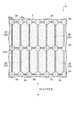
図11は、図10の加工対象物の表面側一部拡大図であり、図12は、図10の加工対象物の裏面側一部拡大図である。図11,12に示すように、加工対象物1は、ストライプ構造の半導体レーザ素子となる矩形板状(外形:600μm×200μm、厚さ:120μm)の半導体レーザ部34が2次元マトリックス状に複数配列されて構成されている。加工対象物1に対しては、半導体レーザ部34,34間においてストライプ方向(半導体レーザ素子におけるレーザ光の共振方向)と直交する方向に延在する切断予定ライン(第1の切断予定ライン)5a、及び半導体レーザ部34,34間においてストライプ方向に延在する切断予定ライン(第2の切断予定ライン)5bが格子状に設定されている。 11 is a partially enlarged view of the front surface side of the processing object of FIG. 10, and FIG. 12 is a partially enlarged view of the back surface side of the processing object of FIG. As shown in FIGS. 11 and 12, the
なお、半導体基板11がGaAsからなる場合には、(011)面及び(0−1−1)面に沿って切断予定ライン5a,5bを設定し、半導体基板11がGaNからなる場合には、(1−100)面及び(−1100)面に沿って切断予定ライン5a,5bを設定する。 When the
アノード電極層32は、図11に示すように、半導体レーザ部34毎に形成された矩形状のアノード電極35を有している。行方向及び列方向にて隣り合うアノード電極35,35は、互いに数μm程度の隙間をとって形成されており、各アノード電極35の四隅には、切欠部35aが形成されている。また、カソード電極層33は、図12に示すように、半導体レーザ部34毎に形成された矩形状のかソード電極36を有している。行方向及び列方向にて隣り合うカソード電極36,36は、互いに数μm程度の隙間をとって形成されており、各カソード電極36においてストライプ方向と直交する二辺には、両端部を残して切欠部36aが形成されている。 As shown in FIG. 11, the
以上のように構成された加工対象物1に対して、本実施形態に係る半導体レーザ素子の製造方法が適用される。 The semiconductor laser device manufacturing method according to this embodiment is applied to the
まず、加工対象物1をレーザ加工装置の支持台(図示せず)上に固定する。そして、図13に示すように、加工対象物1の表面3をレーザ光入射面として半導体基板11の内部に集光点Pを合わせてレーザ光Lを照射し、支持台の移動によって、切断予定ライン5aに沿ってレーザ光Lをスキャンする。このとき、切断予定ライン5aの両側には、数μm程度の隙間をとってアノード電極35が形成されているため、レーザ光Lは、切断予定ライン5aにおいてアノード電極35の切欠部35aに挟まれた部分でのみ半導体基板11の内部に集光される。これにより、図15に示すように、加工対象物1において、切断予定ライン5aに沿った部分のうち、半導体レーザ素子の共振面となる部分34aを除いて、溶融処理領域を含む改質領域7aが切断予定ライン5aに沿って形成されて、切断起点領域(第1の切断起点領域)8aとなる。 First, the
続いて、図14に示すように、加工対象物1の裏面21をレーザ光入射面として半導体基板11の内部に集光点Pを合わせてレーザ光Lを照射し、支持台の移動によって、切断予定ライン5bに沿ってレーザ光Lをスキャンする。このとき、切断予定ライン5bの両側には、数μm程度の隙間をとってカソード電極36が形成されているため、レーザ光Lは、切断予定ライン5bにおいてカソード電極36の切欠部36aに挟まれた部分でのみ半導体基板11の内部に集光される。これにより、図15に示すように、加工対象物1において、切断予定ライン5bに沿った部分のうち、切断予定ライン5aと交差する部分34bを除いて、溶融処理領域を含む改質領域7bが切断予定ライン5bに沿って形成されて、切断起点領域(第2の切断起点領域)8bとなる。 Subsequently, as shown in FIG. 14, the
なお、切断起点領域8bを形成するに際しては、切断起点領域8bを起点として加工対象物1を切断予定ライン5bに沿って切断するのに要する切断力が、切断起点領域8aを起点として加工対象物1を切断予定ライン5aに沿って切断するのに要する切断力よりも大きくなるようにする。具体的には、1本の切断予定ライン5aに対して形成する改質領域7aの列数よりも、1本の切断予定ライン5bに対して形成する改質領域7bの列数を少なくしたり、切断予定ライン5aに沿って照射するレーザ光Lの強度よりも、切断予定ライン5bに沿って照射するレーザ光Lの強度を小さくしたりする。 In forming the cutting
続いて、図16に示すように、切断起点領域8aを起点として加工対象物1を切断予定ライン5aに沿って劈開させることにより、複数の半導体レーザ部34が1次元に配列されたバー37を複数得る。 Subsequently, as shown in FIG. 16, the
そして、図17に示すように、各バー37の劈開面(バー37においてストライプ方向と直交する端面)37aに誘電体膜38を形成する。これにより、半導体レーザ素子の共振面となる部分34aに、保護膜や反射制御膜を効率良く形成することができる。なお、誘電体膜38の形成は、蒸着やスパッタリングによってAl2O3やSi2O3、Si3N4等の誘電体を所定の厚さに積層することで行われる。誘電体膜38は、特に高出力の半導体レーザ素子を製造する場合、一端面側で反射率5%程度の低反射膜とされ、他端面側で反射率95%程度の高反射膜とされる。Then, as shown in FIG. 17, a
続いて、図18に示すように、切断起点領域8bを起点として各バー37を切断予定ライン5bに沿って劈開させることにより、半導体レーザ素子39を複数得る。 Subsequently, as shown in FIG. 18, a plurality of
以上説明したように、本実施形態に係る半導体レーザ素子の製造方法では、加工対象物1に対して、切断予定ライン5aに沿っての切断起点領域8aの形成、及び切断予定ライン5bに沿っての切断起点領域8bの形成の双方を予め行う。ここで、切断起点領域8bは、加工対象物1の内部に集光点Pを合わせてレーザ光Lを照射することにより形成される改質領域7bを有するものであり、しかも、切断予定ライン5bに沿った部分のうち、切断予定ライン5aと交差する部分34bを除いて、切断予定ライン5bに沿って形成される。これにより、切断起点領域8aを起点として加工対象物1を切断する際に、例えば罫書き等に比べて切断起点領域8bの影響力が極めて小さくなり、精度の良い劈開面37aを有するバー37を確実に得ることができる。従って、複数のバー37のそれぞれに対して、切断予定ライン5bに沿っての切断起点領域の形成を行うことが不要となり、半導体レーザ素子39の生産性を向上させることが可能となる。 As described above, in the manufacturing method of the semiconductor laser device according to the present embodiment, the formation of the cutting
また、切断起点領域8a,8bを形成するに際しては、切断起点領域8bを起点として加工対象物1を切断予定ライン5bに沿って切断するのに要する切断力が、切断起点領域8aを起点として加工対象物1を切断予定ライン5aに沿って切断するのに要する切断力よりも大きくなるように、切断予定ライン5bに沿って切断起点領域8bが形成される。これにより、切断起点領域8aを起点として加工対象物1を切断する際に、切断起点領域8bを起点として加工対象物1が切断されるような事態を確実に防止することができる。 Further, when the cutting
更に、切断起点領域8a,8bを形成するに際しては、切断起点領域8bとなる改質領域7bだけでなく、切断起点領域8aとなる改質領域7aも、加工対象物1の内部に集光点Pを合わせてレーザ光Lを照射することにより形成される。この場合、加工対象物1に対する切断起点領域8aの形成及び切断起点領域8bの形成の双方を、レーザ加工装置のみを用いて予め行うことができる。そして、切断起点領域8aは、加工対象物1において、切断予定ライン5aに沿った部分のうち、半導体レーザ素子39の共振面となる部分34aを除いて、切断予定ライン5aに沿って形成される。そのため、半導体レーザ素子39の共振面において、レーザ光が散乱したり、レーザ光の反射率が低下したりするのを防止することができる。 Furthermore, when forming the cutting
なお、半導体基板11とエピタキシャル結晶成長層31との間の格子定数のミスフィットを防止するために半導体基板11がOFF角を有するものである場合、半導体レーザ部34,34間においてストライプ方向に延在する切断予定ライン5bに沿って、罫書きを起点としてバー37を劈開させると、その劈開面が加工対象物1の表面3に対して傾斜することになる。それに対し、本実施形態に係る半導体レーザ素子の製造方法では、切断起点領域8bとして改質領域7bを形成するため、切断予定ライン5bに沿ってバー37を分断させた際における分断面を加工対象物1の表面3に対して略垂直にすることができる。これにより、半導体レーザ素子39においてチッピングの抑制や実装面積の小型化が可能となる。 When the
本発明は、上述した実施形態に限定されるものではない。 The present invention is not limited to the embodiment described above.
例えば、加工対象物1を劈開させることによりバー37を複数得るための切断起点領域5aについては、切断予定ライン5aの両端部等、切断予定ライン5aの少なくとも一部に沿って形成すればよい。なお、切断起点領域5aは、改質領域7aを有するものに限定されず、罫書き等であってもよい。 For example, the cutting
また、遮光性を有するアノード電極35に切欠部35aを設けておくことで、加工対象物1に対し、切断予定ライン5aに沿った部分のうち、半導体レーザ素子39の共振面となる部分34aを除いて、切断予定ライン5aに沿って切断起点領域8aを形成したが、これに限定されない。他の例として、シャッタ等によってレーザ光Lの照射をON/OFFに切り替えたり、レーザ光Lの発振形態をパルス波/CW波に切り替えたりすることで、改質領域7aの形成/非形成を行い、上述したような切断起点領域8aを形成してもよい。このような場合には、アノード電極層32の形成前に切断起点領域8aを形成することができる。以上の点は、切断起点領域8bについても同様である。 In addition, by providing the
なお、数μm程度の隙間をとって切断予定ライン5aの両側にアノード電極35を形成するのは、レーザ光Lの遮光を実現すると共に、切断予定ライン5aに沿って加工対象物1を確実且つ高精度に劈開させるためである。これは、カソード電極36についても同様である。また、半導体レーザ素子39が小型化するほど、レーザ光Lの照射をON/OFFに切り替えたり、レーザ光Lの発振形態をパルス波/CW波に切り替えたりすることが困難となるため、上述したようなアノード電極35及びカソード電極36を形成することは極めて有効である。特にアノード電極35がその四隅に切欠部35aを有しているため、半導体レーザ素子39において適した電圧を印加することが可能となる。 The formation of the
1…加工対象物、5a…切断予定ライン(第1の切断予定ライン)、5b…切断予定ライン(第2の切断予定ライン)、7a,7b…改質領域、8a…切断起点領域(第1の切断起点領域)、8b…切断起点領域(第2の切断起点領域)、34…半導体レーザ部、34a…共振面となる部分、34b…交差する部分、37…バー、37a…劈開面(バーにおいてストライプ方向と直交する端面)、38…誘電体膜、39…半導体レーザ素子、L…レーザ光、P…集光点。 DESCRIPTION OF
Claims (5)
Translated fromJapanese前記半導体レーザ素子となる複数の半導体レーザ部が2次元に配列された加工対象物に対し、前記半導体レーザ部間においてストライプ方向と直交する方向に延在する第1の切断予定ラインの少なくとも一部に沿って、第1の切断起点領域を形成すると共に、前記加工対象物に対し、その内部に集光点を合わせてレーザ光を照射することにより、前記半導体レーザ部間において前記ストライプ方向に延在する第2の切断予定ラインに沿って、改質領域を有する第2の切断起点領域を形成する工程と、
前記第1の切断起点領域を起点として前記加工対象物を前記第1の切断予定ラインに沿って切断することにより、複数の前記半導体レーザ部が1次元に配列されたバーを複数得る工程と、
前記第2の切断起点領域を起点として前記バーを前記第2の切断予定ラインに沿って切断することにより、前記半導体レーザ素子を複数得る工程と、を含み、
前記第1及び前記第2の切断起点領域を形成する工程では、前記第2の切断起点領域を起点として前記加工対象物を前記第2の切断予定ラインに沿って切断するのに要する第2の切断力が、前記第1の切断起点領域を起点として前記加工対象物を前記第1の切断予定ラインに沿って切断するのに要する第1の切断力よりも大きくなるように、前記第2の切断予定ラインに沿って、前記第2の切断起点領域を形成することを特徴とする半導体レーザ素子の製造方法。A method of manufacturing a semiconductor laser device having a stripe structure,
At least a part of a first scheduled cutting line extending in a direction perpendicular to the stripe direction between the semiconductor laser parts with respect to a workpiece in which a plurality of semiconductor laser parts serving as the semiconductor laser elements are two-dimensionally arranged A first cutting start region is formed along the line, and a laser beam is irradiated on the object to be processed with a converging point inside thereof, thereby extending in the stripe direction between the semiconductor laser portions. Forming a second cutting start region having a modified region along a second planned cutting line;
Obtaining a plurality of bars in which a plurality of the semiconductor laser portions are arranged one-dimensionally by cutting the workpiece along the first scheduled cutting line with the first cutting start region as a starting point;
By cutting along the bar the second cutting start region as a start point on the second line to cut,saw including a plurality step of obtaining the semiconductor laserdevice,
In the step of forming the first and second cutting start regions, a second step required to cut the workpiece along the second scheduled cutting line using the second cutting start region as a starting point. The second force is set so that the cutting force is larger than the first cutting force required to cut the workpiece along the first scheduled cutting line from the first cutting starting region. A method of manufacturing a semiconductor laser device, comprising forming the second cutting starting point region along a planned cutting line .
Priority Applications (6)
| Application Number | Priority Date | Filing Date | Title |
|---|---|---|---|
| JP2007231956AJP5225639B2 (en) | 2007-09-06 | 2007-09-06 | Manufacturing method of semiconductor laser device |
| CN2008801060905ACN101796698B (en) | 2007-09-06 | 2008-09-02 | Manufacturing method of semiconductor laser element |
| US12/676,666US8110422B2 (en) | 2007-09-06 | 2008-09-02 | Manufacturing method of semiconductor laser element |
| PCT/JP2008/065760WO2009031534A1 (en) | 2007-09-06 | 2008-09-02 | Manufacturing method of semiconductor laser element |
| KR1020107002282AKR101522746B1 (en) | 2007-09-06 | 2008-09-02 | Manufacturing method of semiconductor laser element |
| TW097134192ATWI464986B (en) | 2007-09-06 | 2008-09-05 | Method for manufacturing semiconductor laser element |
Applications Claiming Priority (1)
| Application Number | Priority Date | Filing Date | Title |
|---|---|---|---|
| JP2007231956AJP5225639B2 (en) | 2007-09-06 | 2007-09-06 | Manufacturing method of semiconductor laser device |
Publications (2)
| Publication Number | Publication Date |
|---|---|
| JP2009064983A JP2009064983A (en) | 2009-03-26 |
| JP5225639B2true JP5225639B2 (en) | 2013-07-03 |
Family
ID=40428850
Family Applications (1)
| Application Number | Title | Priority Date | Filing Date |
|---|---|---|---|
| JP2007231956AActiveJP5225639B2 (en) | 2007-09-06 | 2007-09-06 | Manufacturing method of semiconductor laser device |
Country Status (6)
| Country | Link |
|---|---|
| US (1) | US8110422B2 (en) |
| JP (1) | JP5225639B2 (en) |
| KR (1) | KR101522746B1 (en) |
| CN (1) | CN101796698B (en) |
| TW (1) | TWI464986B (en) |
| WO (1) | WO2009031534A1 (en) |
Families Citing this family (58)
| Publication number | Priority date | Publication date | Assignee | Title |
|---|---|---|---|---|
| JP4659300B2 (en) | 2000-09-13 | 2011-03-30 | 浜松ホトニクス株式会社 | Laser processing method and semiconductor chip manufacturing method |
| TWI326626B (en) | 2002-03-12 | 2010-07-01 | Hamamatsu Photonics Kk | Laser processing method |
| EP2400539B1 (en) | 2002-03-12 | 2017-07-26 | Hamamatsu Photonics K.K. | Substrate dividing method |
| WO2003076119A1 (en) | 2002-03-12 | 2003-09-18 | Hamamatsu Photonics K.K. | Method of cutting processed object |
| TWI520269B (en) | 2002-12-03 | 2016-02-01 | Hamamatsu Photonics Kk | Cutting method of semiconductor substrate |
| FR2852250B1 (en) | 2003-03-11 | 2009-07-24 | Jean Luc Jouvin | PROTECTIVE SHEATH FOR CANNULA, AN INJECTION KIT COMPRISING SUCH ANKLE AND NEEDLE EQUIPPED WITH SUCH ANKLE |
| DE60315515T2 (en) | 2003-03-12 | 2007-12-13 | Hamamatsu Photonics K.K., Hamamatsu | LASER PROCESSING PROCEDURES |
| CN101862907B (en)* | 2003-07-18 | 2014-01-22 | 浜松光子学株式会社 | Laser beam machining method, laser beam machining apparatus, and laser machined product |
| JP4563097B2 (en) | 2003-09-10 | 2010-10-13 | 浜松ホトニクス株式会社 | Semiconductor substrate cutting method |
| JP4601965B2 (en)* | 2004-01-09 | 2010-12-22 | 浜松ホトニクス株式会社 | Laser processing method and laser processing apparatus |
| JP4598407B2 (en)* | 2004-01-09 | 2010-12-15 | 浜松ホトニクス株式会社 | Laser processing method and laser processing apparatus |
| JP4509578B2 (en) | 2004-01-09 | 2010-07-21 | 浜松ホトニクス株式会社 | Laser processing method and laser processing apparatus |
| EP1742253B1 (en) | 2004-03-30 | 2012-05-09 | Hamamatsu Photonics K.K. | Laser processing method |
| KR101109860B1 (en)* | 2004-08-06 | 2012-02-21 | 하마마츠 포토닉스 가부시키가이샤 | Laser processing method, cutting method for work and semiconductor device |
| JP4762653B2 (en)* | 2005-09-16 | 2011-08-31 | 浜松ホトニクス株式会社 | Laser processing method and laser processing apparatus |
| JP4907965B2 (en)* | 2005-11-25 | 2012-04-04 | 浜松ホトニクス株式会社 | Laser processing method |
| JP4804911B2 (en)* | 2005-12-22 | 2011-11-02 | 浜松ホトニクス株式会社 | Laser processing equipment |
| JP4907984B2 (en) | 2005-12-27 | 2012-04-04 | 浜松ホトニクス株式会社 | Laser processing method and semiconductor chip |
| JP5183892B2 (en) | 2006-07-03 | 2013-04-17 | 浜松ホトニクス株式会社 | Laser processing method |
| EP1875983B1 (en) | 2006-07-03 | 2013-09-11 | Hamamatsu Photonics K.K. | Laser processing method and chip |
| CN101516566B (en)* | 2006-09-19 | 2012-05-09 | 浜松光子学株式会社 | Laser processing method and laser processing apparatus |
| JP4954653B2 (en) | 2006-09-19 | 2012-06-20 | 浜松ホトニクス株式会社 | Laser processing method |
| JP5101073B2 (en)* | 2006-10-02 | 2012-12-19 | 浜松ホトニクス株式会社 | Laser processing equipment |
| JP4964554B2 (en)* | 2006-10-03 | 2012-07-04 | 浜松ホトニクス株式会社 | Laser processing method |
| JP5132911B2 (en)* | 2006-10-03 | 2013-01-30 | 浜松ホトニクス株式会社 | Laser processing method |
| WO2008041604A1 (en)* | 2006-10-04 | 2008-04-10 | Hamamatsu Photonics K.K. | Laser processing method |
| JP5336054B2 (en)* | 2007-07-18 | 2013-11-06 | 浜松ホトニクス株式会社 | Processing information supply system provided with processing information supply device |
| JP5449665B2 (en)* | 2007-10-30 | 2014-03-19 | 浜松ホトニクス株式会社 | Laser processing method |
| JP5134928B2 (en)* | 2007-11-30 | 2013-01-30 | 浜松ホトニクス株式会社 | Workpiece grinding method |
| JP5054496B2 (en)* | 2007-11-30 | 2012-10-24 | 浜松ホトニクス株式会社 | Processing object cutting method |
| JP5692969B2 (en) | 2008-09-01 | 2015-04-01 | 浜松ホトニクス株式会社 | Aberration correction method, laser processing method using this aberration correction method, laser irradiation method using this aberration correction method, aberration correction apparatus, and aberration correction program |
| JP5254761B2 (en) | 2008-11-28 | 2013-08-07 | 浜松ホトニクス株式会社 | Laser processing equipment |
| JP5241527B2 (en) | 2009-01-09 | 2013-07-17 | 浜松ホトニクス株式会社 | Laser processing equipment |
| JP5241525B2 (en) | 2009-01-09 | 2013-07-17 | 浜松ホトニクス株式会社 | Laser processing equipment |
| KR101757937B1 (en) | 2009-02-09 | 2017-07-13 | 하마마츠 포토닉스 가부시키가이샤 | Workpiece cutting method |
| JP5639997B2 (en) | 2009-04-07 | 2014-12-10 | 浜松ホトニクス株式会社 | Laser processing equipment |
| JP5491761B2 (en) | 2009-04-20 | 2014-05-14 | 浜松ホトニクス株式会社 | Laser processing equipment |
| JP2011035253A (en)* | 2009-08-04 | 2011-02-17 | Disco Abrasive Syst Ltd | Method of processing wafer |
| JP5379604B2 (en)* | 2009-08-21 | 2013-12-25 | 浜松ホトニクス株式会社 | Laser processing method and chip |
| JP5653110B2 (en)* | 2010-07-26 | 2015-01-14 | 浜松ホトニクス株式会社 | Chip manufacturing method |
| US8722516B2 (en) | 2010-09-28 | 2014-05-13 | Hamamatsu Photonics K.K. | Laser processing method and method for manufacturing light-emitting device |
| JP5670764B2 (en)* | 2011-01-13 | 2015-02-18 | 浜松ホトニクス株式会社 | Laser processing method |
| JP6013859B2 (en)* | 2012-10-01 | 2016-10-25 | 株式会社ディスコ | Wafer processing method |
| JP6147982B2 (en)* | 2012-10-09 | 2017-06-14 | 株式会社ディスコ | Wafer processing method |
| JP6059059B2 (en) | 2013-03-28 | 2017-01-11 | 浜松ホトニクス株式会社 | Laser processing method |
| US9812361B2 (en)* | 2013-09-11 | 2017-11-07 | Nxp B.V. | Combination grinding after laser (GAL) and laser on-off function to increase die strength |
| CN107148324A (en)* | 2014-08-28 | 2017-09-08 | Ipg光子公司 | Multiple laser systems and methods for dicing and post-dicing machining of hard dielectric materials |
| JP6384532B2 (en) | 2016-08-29 | 2018-09-05 | 日亜化学工業株式会社 | Method for manufacturing light emitting device |
| JP6931277B2 (en)* | 2016-08-31 | 2021-09-01 | 三洋電機株式会社 | Method for manufacturing electrodes for secondary batteries and method for manufacturing secondary batteries |
| JP6821245B2 (en)* | 2016-10-11 | 2021-01-27 | 株式会社ディスコ | Wafer processing method |
| JP6957187B2 (en)* | 2017-04-18 | 2021-11-02 | 浜松ホトニクス株式会社 | Chip manufacturing method and silicon chip |
| US10589445B1 (en)* | 2018-10-29 | 2020-03-17 | Semivation, LLC | Method of cleaving a single crystal substrate parallel to its active planar surface and method of using the cleaved daughter substrate |
| JP2020072220A (en)* | 2018-11-01 | 2020-05-07 | 株式会社ディスコ | Processing method of work piece |
| US20220059994A1 (en)* | 2018-12-13 | 2022-02-24 | Sony Group Corporation | Semiconductor apparatus and method for manufacturing semiconductor apparatus |
| US10562130B1 (en) | 2018-12-29 | 2020-02-18 | Cree, Inc. | Laser-assisted method for parting crystalline material |
| US10576585B1 (en) | 2018-12-29 | 2020-03-03 | Cree, Inc. | Laser-assisted method for parting crystalline material |
| US11024501B2 (en) | 2018-12-29 | 2021-06-01 | Cree, Inc. | Carrier-assisted method for parting crystalline material along laser damage region |
| US10611052B1 (en) | 2019-05-17 | 2020-04-07 | Cree, Inc. | Silicon carbide wafers with relaxed positive bow and related methods |
Family Cites Families (12)
| Publication number | Priority date | Publication date | Assignee | Title |
|---|---|---|---|---|
| US6211488B1 (en)* | 1998-12-01 | 2001-04-03 | Accudyne Display And Semiconductor Systems, Inc. | Method and apparatus for separating non-metallic substrates utilizing a laser initiated scribe |
| JP4659300B2 (en) | 2000-09-13 | 2011-03-30 | 浜松ホトニクス株式会社 | Laser processing method and semiconductor chip manufacturing method |
| JP2002289955A (en)* | 2001-03-23 | 2002-10-04 | Sharp Corp | Semiconductor laser element, manufacturing method therefor and optical information reproducing device |
| JP2003017791A (en) | 2001-07-03 | 2003-01-17 | Sharp Corp | Nitride semiconductor device and method for manufacturing the nitride semiconductor device |
| JP2003086900A (en)* | 2001-09-07 | 2003-03-20 | Toshiba Electronic Engineering Corp | Semiconductor laser device and method of manufacturing semiconductor laser device |
| WO2003076119A1 (en) | 2002-03-12 | 2003-09-18 | Hamamatsu Photonics K.K. | Method of cutting processed object |
| JP2003338468A (en)* | 2002-03-12 | 2003-11-28 | Hamamatsu Photonics Kk | Manufacturing method of light-emitting element, light- emitting diode, and semiconductor laser element |
| US20060209395A1 (en)* | 2003-03-26 | 2006-09-21 | Nec Corporation | Semiconductor laser and method for manufacturing the same |
| US7408199B2 (en)* | 2004-04-02 | 2008-08-05 | Nichia Corporation | Nitride semiconductor laser device and nitride semiconductor device |
| JP4767711B2 (en) | 2006-02-16 | 2011-09-07 | 株式会社ディスコ | Wafer division method |
| JP4430689B2 (en)* | 2007-05-28 | 2010-03-10 | 日亜化学工業株式会社 | Manufacturing method of nitride semiconductor laser device |
| JP5449665B2 (en) | 2007-10-30 | 2014-03-19 | 浜松ホトニクス株式会社 | Laser processing method |
- 2007
- 2007-09-06JPJP2007231956Apatent/JP5225639B2/enactiveActive
- 2008
- 2008-09-02WOPCT/JP2008/065760patent/WO2009031534A1/enactiveApplication Filing
- 2008-09-02KRKR1020107002282Apatent/KR101522746B1/enactiveActive
- 2008-09-02USUS12/676,666patent/US8110422B2/enactiveActive
- 2008-09-02CNCN2008801060905Apatent/CN101796698B/enactiveActive
- 2008-09-05TWTW097134192Apatent/TWI464986B/enactive
Also Published As
| Publication number | Publication date |
|---|---|
| CN101796698A (en) | 2010-08-04 |
| US20100240159A1 (en) | 2010-09-23 |
| KR20100052467A (en) | 2010-05-19 |
| TW200919882A (en) | 2009-05-01 |
| US8110422B2 (en) | 2012-02-07 |
| KR101522746B1 (en) | 2015-05-26 |
| CN101796698B (en) | 2012-06-27 |
| JP2009064983A (en) | 2009-03-26 |
| WO2009031534A1 (en) | 2009-03-12 |
| TWI464986B (en) | 2014-12-11 |
Similar Documents
| Publication | Publication Date | Title |
|---|---|---|
| JP5225639B2 (en) | Manufacturing method of semiconductor laser device | |
| JP4198123B2 (en) | Laser processing method | |
| JP5449665B2 (en) | Laser processing method | |
| JP5054496B2 (en) | Processing object cutting method | |
| JP4200177B2 (en) | Laser processing method and semiconductor device | |
| JP4829781B2 (en) | Laser processing method and semiconductor chip | |
| KR101349556B1 (en) | Laser processing method and laser processing device | |
| KR101455408B1 (en) | Laser processing method | |
| KR101428823B1 (en) | Laser processing method and laser processing apparatus | |
| JP5312761B2 (en) | Cutting method | |
| JP4907984B2 (en) | Laser processing method and semiconductor chip | |
| JP5138219B2 (en) | Laser processing method | |
| JP4634089B2 (en) | Laser processing method | |
| JP5322418B2 (en) | Laser processing method and laser processing apparatus | |
| WO2008004394A1 (en) | Laser working method | |
| JP5122161B2 (en) | Processing object cutting method |
Legal Events
| Date | Code | Title | Description |
|---|---|---|---|
| A621 | Written request for application examination | Free format text:JAPANESE INTERMEDIATE CODE: A621 Effective date:20100902 | |
| A131 | Notification of reasons for refusal | Free format text:JAPANESE INTERMEDIATE CODE: A131 Effective date:20121106 | |
| A521 | Request for written amendment filed | Free format text:JAPANESE INTERMEDIATE CODE: A523 Effective date:20121225 | |
| TRDD | Decision of grant or rejection written | ||
| A01 | Written decision to grant a patent or to grant a registration (utility model) | Free format text:JAPANESE INTERMEDIATE CODE: A01 Effective date:20130212 | |
| A61 | First payment of annual fees (during grant procedure) | Free format text:JAPANESE INTERMEDIATE CODE: A61 Effective date:20130313 | |
| R150 | Certificate of patent or registration of utility model | Ref document number:5225639 Country of ref document:JP Free format text:JAPANESE INTERMEDIATE CODE: R150 Free format text:JAPANESE INTERMEDIATE CODE: R150 | |
| FPAY | Renewal fee payment (event date is renewal date of database) | Free format text:PAYMENT UNTIL: 20160322 Year of fee payment:3 | |
| R250 | Receipt of annual fees | Free format text:JAPANESE INTERMEDIATE CODE: R250 | |
| R250 | Receipt of annual fees | Free format text:JAPANESE INTERMEDIATE CODE: R250 |