JP5224837B2 - Substrate plasma processing apparatus and plasma processing method - Google Patents
Substrate plasma processing apparatus and plasma processing methodDownload PDFInfo
- Publication number
- JP5224837B2 JP5224837B2JP2008023066AJP2008023066AJP5224837B2JP 5224837 B2JP5224837 B2JP 5224837B2JP 2008023066 AJP2008023066 AJP 2008023066AJP 2008023066 AJP2008023066 AJP 2008023066AJP 5224837 B2JP5224837 B2JP 5224837B2
- Authority
- JP
- Japan
- Prior art keywords
- substrate
- frequency voltage
- negative pulse
- applying means
- high frequency
- Prior art date
- Legal status (The legal status is an assumption and is not a legal conclusion. Google has not performed a legal analysis and makes no representation as to the accuracy of the status listed.)
- Active
Links
Images


Classifications
- H—ELECTRICITY
- H01—ELECTRIC ELEMENTS
- H01J—ELECTRIC DISCHARGE TUBES OR DISCHARGE LAMPS
- H01J37/00—Discharge tubes with provision for introducing objects or material to be exposed to the discharge, e.g. for the purpose of examination or processing thereof
- H01J37/32—Gas-filled discharge tubes
- H01J37/32009—Arrangements for generation of plasma specially adapted for examination or treatment of objects, e.g. plasma sources
- H01J37/32018—Glow discharge
- H01J37/32027—DC powered
- H—ELECTRICITY
- H01—ELECTRIC ELEMENTS
- H01J—ELECTRIC DISCHARGE TUBES OR DISCHARGE LAMPS
- H01J37/00—Discharge tubes with provision for introducing objects or material to be exposed to the discharge, e.g. for the purpose of examination or processing thereof
- H01J37/32—Gas-filled discharge tubes
- H01J37/32009—Arrangements for generation of plasma specially adapted for examination or treatment of objects, e.g. plasma sources
- H01J37/32018—Glow discharge
- H01J37/32045—Circuits specially adapted for controlling the glow discharge
- H—ELECTRICITY
- H01—ELECTRIC ELEMENTS
- H01J—ELECTRIC DISCHARGE TUBES OR DISCHARGE LAMPS
- H01J37/00—Discharge tubes with provision for introducing objects or material to be exposed to the discharge, e.g. for the purpose of examination or processing thereof
- H01J37/32—Gas-filled discharge tubes
- H01J37/32009—Arrangements for generation of plasma specially adapted for examination or treatment of objects, e.g. plasma sources
- H01J37/32082—Radio frequency generated discharge
- H01J37/32091—Radio frequency generated discharge the radio frequency energy being capacitively coupled to the plasma
Landscapes
- Physics & Mathematics (AREA)
- Engineering & Computer Science (AREA)
- Plasma & Fusion (AREA)
- Chemical & Material Sciences (AREA)
- Analytical Chemistry (AREA)
- Plasma Technology (AREA)
- Drying Of Semiconductors (AREA)
- Chemical Vapour Deposition (AREA)
Description
Translated fromJapanese本発明は、真空チャンバー内において、RF電極と対向電極とが互いに対向するように配置され、それらの間に生成されたプラズマによってRF電極上に保持された基板を加工する、いわゆる平行平板型の基板のプラズマ処理装置及びプラズマ処理方法に関する。 The present invention is a so-called parallel plate type in which a RF electrode and a counter electrode are arranged so as to face each other in a vacuum chamber, and a substrate held on the RF electrode is processed by plasma generated therebetween. The present invention relates to a substrate plasma processing apparatus and a plasma processing method.
半導体ウエハなどの基板に対して配線などを行う際には、基板に対して微細な加工処理を施す必要があり、そのため、従来では、プラズマを用いたプラズマ処理装置が頻繁に用いられていた。 When wiring or the like is performed on a substrate such as a semiconductor wafer, it is necessary to perform fine processing on the substrate. Therefore, conventionally, a plasma processing apparatus using plasma has been frequently used.
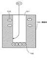
図11は、このような従来の基板のプラズマ処理装置の一例における構成を概略的に示す図である。 FIG. 11 is a diagram schematically showing the configuration of an example of such a conventional substrate plasma processing apparatus.
図11に示す基板のプラズマ処理装置10においては、予め所定の真空度まで排気されたチャンバー11内に、高周波(RF)電極12と対向電極13とが互いに対向するようにして配置され、RF電極12の、対向電極13と対向する主面上に処理に供すべき基板Sが保持され、いわゆる平行平板型のプラズマ処理装置を構成している。ガス導入管14からはプラズマ生成及びそれによって基板Sの加工に供すべきガスを矢印で示すようにしてチャンバー11内に導入するとともに、図示しない真空ポンプを用いて、排気口15からチャンバー11内を真空排気する。このとき、チャンバー11内の圧力は例えば約1Pa程度とする。 In the substrate
次いで、13.56MHzの商業用RF電源17から整合器16を介してRF電極12にRF(電圧)を印加することにより、RF電極12及び対向電極13間にプラズマPを生ぜしめるようにしている。 Next, RF (voltage) is applied to the
この際、プラズマP中の正イオンはRF電極12上に生じる負の自己バイアス電位VdcによってRF電極12上の基板Sに高速で入射するようになる。その結果、その際の基板入射エネルギーを利用して基板S上の表面反応を誘発し、リアクティブイオンエッチング(RIE)、PCVD(Plaslma Chemical Vapor Deposition)、スパッタリング、イオンインプラ等のプラズマ基板処理が行われる。特に、基板を加工するという観点からは、主としてRIEが用いられる。したがって、以下では、特にRIEを用いた基板処理を中心として詳述する。 At this time, positive ions in the plasma P are incident on the substrate S on the
図11に示すようなプラズマ処理装置においては、図12に示すように、RFパワー増大とともにVdc(平均の基板入射エネルギー)は増大するため、処理レート調整、加工形状調整のために主にRFパワーによるVdcの調整が行われている。またVdcが依存する圧力や電極形状でも一部調整することができる。 In the plasma processing apparatus as shown in FIG. 11, Vdc (average substrate incident energy) increases as the RF power increases as shown in FIG. 12, and therefore the RF power is mainly used to adjust the processing rate and the processing shape. Vdc is adjusted by the above. Further, the pressure and electrode shape on which Vdc depends can be partially adjusted.
図13、図14は13MHz、Vrf=160V、6.6pa、電極間30mm、300mmウエハサイズの平行平板型Arプラズマを連続体モデルプラズマシミュレータ(G. Chen, L. L. Raja, J. Appl. Phys. 96, 6073(2004))でシミュレーションした結果である。また、図15は、基板SのRIEに対して適したイオンエネルギーの分布状態を示したグラフである。 13 and 14 show a parallel model Ar plasma of 13 MHz, Vrf = 160 V, 6.6 pa, 30 mm between electrodes, 300 mm wafer size (G. Chen, LL Raja, J. Appl. Phys. 96). , 6073 (2004)). FIG. 15 is a graph showing ion energy distribution suitable for RIE of the substrate S.
図13に示すように、RF電極電位が周期的に変動するためイオンの基板入射エネルギーも周期的に変動する。ただしイオン質量による電位への追従遅れがあるため、Vrfより小さい振幅Vrf´でイオンエネルギーは時間変動する。イオンエネルギーは正確にはVdcとプラズマポテンシャルVpの和になるが、Vpの値及び時間変化が相対的に小さいので説明及び図13では省略している。そのため基板Sへの入射エネルギーは、図13に示すグラフを時間積分することにより、図14で示されるようなイオンエネルギー分布となる。 As shown in FIG. 13, since the RF electrode potential periodically changes, the ion incident energy of the ions also periodically changes. However, since there is a delay in tracking the potential due to the ion mass, the ion energy varies with time at an amplitude Vrf ′ smaller than Vrf. The ion energy is precisely the sum of Vdc and plasma potential Vp, but is omitted in the description and FIG. 13 because the value of Vp and the change with time are relatively small. Therefore, the incident energy to the substrate S becomes an ion energy distribution as shown in FIG. 14 by time-integrating the graph shown in FIG.
図14から明らかなように、図11に示すような装置内に生成されたプラズマ内のイオンエネルギーは、低エネルギー側ピークと高エネルギー側ピークとの2つに分割され、そのエネルギー幅ΔEはプラズマ発生条件によって数10〜数100[eV]と広くなる。したがって、Vdcを基板処理に最適なエネルギーに調整した場合においても、図15に示すように基板入射するイオンにはエネルギーの高すぎるイオン(高エネルギー側ピーク)と低すぎるイオン(低エネルギー側ピーク)とが存在するようになる。 As is clear from FIG. 14, the ion energy in the plasma generated in the apparatus as shown in FIG. 11 is divided into two peaks, a low energy side peak and a high energy side peak, and the energy width ΔE is the plasma. Depending on the generation conditions, it becomes as wide as several tens to several hundreds [eV]. Therefore, even when Vdc is adjusted to an optimum energy for substrate processing, as shown in FIG. 15, ions that are too energy (high energy peak) and ions that are too low (low energy peak) for ions incident on the substrate. And come to exist.
したがって、例えばRIEにおいては、高エネルギー側ピークに相当するエネルギーのイオンで基板処理を実施した場合は、肩削り(肩落ち)を誘発して加工形状を悪化させる傾向がある。一方、低エネルギー側ピークに相当するエネルギーのイオンで基板処理を実施した場合は、表面反応閾値以下で基板処理にまったく寄与しない、あるいは異方性劣化 (イオン入射角度が熱速度で広がる)に伴い加工形状を悪化させる傾向がある。 Therefore, for example, in RIE, when substrate processing is performed with ions having an energy corresponding to a high energy side peak, there is a tendency to induce shoulder shaving (shoulder fall) and deteriorate the processing shape. On the other hand, when substrate processing is performed with ions with energy corresponding to the low energy side peak, it does not contribute to the substrate processing at all below the surface reaction threshold, or due to anisotropy degradation (the ion incident angle spreads with the thermal velocity). There is a tendency to deteriorate the processing shape.
かかる観点より、最近の半導体プロセスにおいては、ますますシュリンクしていく半導体デバイス・種々の膜・複合膜のRIEに対応し、加工形状を精緻に制御するため、図15の略中心部に斜線で示したようなイオンエネルギーの狭帯域化(小さいΔEの実現)と平均エネルギー値の最適調整(Vdcの最適化)が必要となる。 From such a viewpoint, in recent semiconductor processes, in order to precisely control the processing shape in response to the RIE of semiconductor devices, various films, and composite films that are shrinking more and more, a hatching is applied to the approximate center of FIG. It is necessary to narrow the ion energy band as shown (realization of small ΔE) and optimal adjustment of the average energy value (optimization of Vdc).
イオンエネルギー狭帯域化のためには、RF周波数の高周波化(例えば、特許文献1参照。)やパルスプラズマ化(例えば、非特許文献1参照。)が検討されている。 In order to narrow the ion energy band, high frequency RF (for example, refer to Patent Document 1) and pulse plasma (for example, refer to Non-Patent Document 1) have been studied.
また、プラズマ生成は大きく分けて誘導結合型と容量結合型に大別されるが、加工形状の精密制御の観点から、副次反応を抑制するためにプラズマ体積を小さくして滞留時間を小さくすることが有効であり、このような観点から、体積の大きな誘導結合型プラズマと比較して容量結合型の平行平板型プラズマが有利である。 Plasma generation is roughly divided into inductive coupling type and capacitive coupling type. From the viewpoint of precise control of the processing shape, the plasma volume is reduced to reduce the residence time in order to suppress side reactions. From this point of view, the capacitively coupled parallel plate type plasma is more advantageous than the large volume inductively coupled plasma.
また、Vdcとプラズマ密度の制御性向上を目的に平行平板の電極に2つの異なる周波数のRFを導入し、高い周波数(例えば100MHz)のRFでプラズマ密度を、低い周波数(例えば3MHz)のRFでVdcを独立制御する方法も考案されている(例えば、特許文献1参照。)。この場合は、高周波用電源及び高周波用整合器に加えて、低周波用電源及び低周波用電源とを設け、上述した高周波のRF及び低周波のRFがRF電極に対して重畳できるようにしている。 In addition, for the purpose of improving controllability of Vdc and plasma density, two different frequency RFs are introduced into parallel plate electrodes, and the plasma density is increased with a high frequency (for example, 100 MHz) RF and the RF with a low frequency (for example, 3 MHz). A method of independently controlling Vdc has also been devised (see, for example, Patent Document 1). In this case, in addition to the high frequency power source and the high frequency matching unit, a low frequency power source and a low frequency power source are provided so that the above-described high frequency RF and low frequency RF can be superimposed on the RF electrode. Yes.
清浄プロセス、プロセス安定の観点から対向電極は接地電位であることが有利となる。対向電極にRFを引加すると対向電極面で生成するVdcにより対向電極が腐食し、ダスト源、プロセスを不安定化源となる。そのため、2つのRFは基板が設置されたRF電極に重畳される。 From the viewpoint of the cleaning process and process stability, the counter electrode is advantageously at ground potential. When RF is applied to the counter electrode, the counter electrode corrodes due to Vdc generated on the counter electrode surface, and the dust source and the process become an unstable source. Therefore, the two RFs are superimposed on the RF electrode on which the substrate is installed.
また、RFのパルス化により、電子温度の低下を図ること(例えば、非特許文献2参照。)、プロセス阻害ラジカル(例えばフッ素ラジカル)密度の抑制を図ること(例えば、非特許文献3参照。)、プラズマエッチングの選択性(例えば、シリコン酸化/シリコンエッチングレート選択比)の向上を図ること(例えば、非特許文献4参照。)が試みられている。
上記したとおり、従来から周波数の高い高周波電力(HF)のパルス化や、周波数の高い高周波電力(HF)と周波数の低い高周波電力(LF)との重畳印加などにより、ラジカル密度を制御し、電子温度低下によるプラズマダメージの抑制等を図ることが試みられている。 As described above, the radical density is controlled by pulsing the high frequency power (HF) having a high frequency or by superimposing the high frequency power (HF) having a high frequency and the high frequency power (LF) having a low frequency. Attempts have been made to suppress plasma damage due to a decrease in temperature.
また、本発明者等は、周波数の高い高周波電力(HF)にDC負パルスを重畳印加することを検討している。この技術では、DC負パルスを重畳印加することにより、正イオンエネルギーが狭帯域化して、プロセスに望ましいエネルギー帯に容易に制御され、プラズマエッチングの加工精度向上、プラズマダメージ抑制、プラズマCVDの埋め込み特性向上が成される。一方、HF(RF)のパルス化により、ラジカル密度が制御され、電子温度低下によるプラズマダメージ抑制が期待される。 In addition, the present inventors are considering applying a DC negative pulse superimposed on high-frequency power (HF) having a high frequency. In this technology, by applying a DC negative pulse in a superimposed manner, the positive ion energy is narrowed and easily controlled to the energy band desired for the process, improving plasma etching processing accuracy, suppressing plasma damage, and embedding characteristics of plasma CVD. Improvements are made. On the other hand, radical density is controlled by HF (RF) pulsing, and plasma damage suppression due to a decrease in electron temperature is expected.
DC負パルスとパルス化された周波数の高い高周波電力(HF)を重畳印加したことにより、例えば、CH4ガスによる酸化膜の異方性エッチングにおいては、Fラジカル密度が減少(等方性エッチング減少)し、CF3+等のイオンラジカルによる違方性エッチングが増大して、なおかつイオンエネルギーが狭帯域に制御される。また側壁保護膜(異方性促進)生成源となるCF2等のラジカル密度が増大する。このラジカル種選択作用、エネルギーの選択作用により、プロセス制御性向上とともに、格段の加工性能向上が成される。By applying DC negative pulse and pulsed high frequency high frequency power (HF), for example, in anisotropic etching of oxide film with CH4 gas, F radical density is reduced (isotropic etching is reduced). ) And anisotropic etching due to ion radicals such as CF3+ increases, and the ion energy is controlled in a narrow band. In addition, the density of radicals such as CF2 serving as a side wall protective film (anisotropy promotion) generation source increases. By this radical species selection action and energy selection action, the process controllability is improved and the processing performance is remarkably improved.
しかし、後述する図7(パルス化したHFとDC負パルスを重畳印加した際のプラズマ密度、電子温度、およびプロセスの時間変化をシミュレーションした解析結果)に示すように、高周波電力(HF)のオフとともに電子温度は極めて短時間に(〜5e−6秒)低下して電子衝突・イオン化によるイオン発生、電子発生は停止する。その、いわゆるアフターグローの状態においてDC負パルスを印加するとプラズマ中の電子、イオンがプラズマ外に引き出され、プラズマは不安定となり、消滅してしまう。プラズマの消滅はプロセスレートの減少、再着火時のデバイスダメージ、プロセス不安定化を誘発する。また、図9に示すように、DC負パルスを用いた酸化膜、窒化膜等の絶縁体100の加工時、トレンチ溝101の底部102において電子不足によるチャージアップが起こる場合がある。そして、このようなチャージアップが起きると、イオン曲がりによる加工形状悪化、エッチングストップ、またチャージ電圧によるデバイスへのダメージを誘発する。 However, as shown in FIG. 7 (analysis result simulating plasma density, electron temperature, and process change over time when pulsed HF and DC negative pulses are superimposed and applied), the high-frequency power (HF) is turned off. At the same time, the electron temperature decreases in an extremely short time (˜5e-6 seconds), and ion generation and electron generation due to electron collision and ionization stop. When a DC negative pulse is applied in the so-called afterglow state, electrons and ions in the plasma are drawn out of the plasma, and the plasma becomes unstable and disappears. Plasma extinction induces a decrease in process rate, device damage during re-ignition, and process instability. In addition, as shown in FIG. 9, when processing the
本発明は、上述した従来の事情に鑑みてなされたものであり、いわゆる平行平板型プラズマ処理装置において、基板の加工に適したラジカル種密度を増大させ、イオンラジカルエネルギーを基板の加工に適したエネルギー値、狭帯域エネルギー幅に制御して、精緻加工を行うことができ、また、優れた埋め込み成膜を行うことが可能な基板のプラズマ処理装置及びプラズマ処理方法を提供することを目的とする。 The present invention has been made in view of the above-described conventional circumstances. In a so-called parallel plate type plasma processing apparatus, the radical species density suitable for substrate processing is increased, and ion radical energy is suitable for substrate processing. An object of the present invention is to provide a plasma processing apparatus and a plasma processing method for a substrate, which can be precisely processed by controlling the energy value and the narrow band energy width, and can perform excellent embedded film formation. .
本発明の基板のプラズマ処理装置の一態様は、内部を真空に保持可能とされたチャンバーと、前記チャンバー内に配置され、主面上において処理すべき基板を保持するように構成された基板保持電極と、前記チャンバー内において、前記基板保持電極と対向するように配置された対向電極と、前記基板保持電極に対して50MHz以上の所定周波数の高周波電圧を印加するための高周波電圧印加手段と、前記基板保持電極に対して前記高周波電圧と重畳するようにして所定のDC負パルス電圧を印加するためのDC負パルス電圧印加手段と、前記高周波電圧印加手段のオン・オフを所定タイミングで行い、前記高周波電圧の印加が間欠的に行われるよう制御するとともに、当該高周波電圧印加手段のオン・オフのタイミングに応じて前記DC負パルス電圧印加手段のオン・オフを制御し、前記DC負パルス電圧の印加が間欠的に行われるよう制御し、かつ、前記高周波電圧印加手段のオフ以前に、前記DC負パルス電圧印加手段をオフとする制御手段とを備えたことを特徴とする。
本発明の基板のプラズマ処理装置の他の態様は、内部を真空に保持可能とされたチャンバーと、前記チャンバー内に配置され、主面上において処理すべき基板を保持するように構成された基板保持電極と、前記チャンバー内において、前記基板保持電極と対向するように配置された対向電極と、前記基板保持電極に対して50MHz以上の所定周波数の高周波電圧を印加するための高周波電圧印加手段と、前記基板保持電極に対して前記高周波電圧と重畳するようにして所定のDC負パルス電圧を印加するためのDC負パルス電圧印加手段と、前記高周波電圧印加手段のオン・オフを所定タイミングで行い、前記高周波電圧の印加が間欠的に行われるよう制御するとともに、当該高周波電圧印加手段のオン・オフのタイミングに応じて前記DC負パルス電圧印加手段のオン・オフを制御し、前記DC負パルス電圧の印加が間欠的に行われるよう制御し、かつ、前記高周波電圧印加手段のオン以降に、前記DC負パルス電圧印加手段をオンとする制御手段とを備えたことを特徴とする。One aspect of the substrate plasma processing apparatus of the present invention is a substrate holding apparatus configured to hold a substrate to be processed on a main surface, the chamber being configured to be able to hold the inside in a vacuum, and the chamber. An electrode, a counter electrode disposed so as to face the substrate holding electrode in the chamber, and a high frequency voltage applying means for applying a high frequency voltage of a predetermined frequency of 50 MHz or more to the substrate holding electrode; DC negative pulse voltage applying means for applying a predetermined DC negative pulse voltage to the substrate holding electrode so as to be superimposed on the high frequency voltage, and turning on and off the high frequency voltage applying means at a predetermined timing, The high-frequency voltage is controlled to be intermittently applied, and the DC voltage is controlled according to the on / off timing of the high-frequency voltage application means. Controls the on-off of the pulse voltage applying means, the DC application of the negative pulse voltage is controlledto be intermittentlyperformed, and turned off before the high-frequency voltage applying means, turning off the DC negative pulse voltage applying means And a control means.
In another aspect of the substrate plasma processing apparatus of the present invention, a chamber capable of maintaining the inside in a vacuum, and a substrate disposed in the chamber and configured to hold a substrate to be processed on a main surface. A holding electrode; a counter electrode arranged to face the substrate holding electrode in the chamber; and a high frequency voltage applying means for applying a high frequency voltage of a predetermined frequency of 50 MHz or more to the substrate holding electrode. DC negative pulse voltage applying means for applying a predetermined DC negative pulse voltage to the substrate holding electrode so as to be superimposed on the high frequency voltage, and turning on / off the high frequency voltage applying means at a predetermined timing. The high frequency voltage is controlled to be intermittently applied, and the high frequency voltage applying means is turned on / off according to the on / off timing. The negative pulse voltage application means is controlled to be turned on / off, the negative DC voltage pulse is applied intermittently, and the negative DC voltage pulse application means is turned on after the high frequency voltage application means is turned on. And a control means for turning on.
本発明の基板のプラズマ処理方法の一態様は、内部を真空に保持可能とされたチャンバーと、前記チャンバー内に配置され、主面上において処理すべき基板を保持するように構成された基板保持電極と、前記チャンバー内において、前記基板保持電極と対向するように配置された対向電極と、前記基板保持電極に対して50MHz以上の所定周波数の高周波電圧を印加するための高周波電圧印加手段と、前記基板保持電極に対して前記高周波電圧と重畳するようにして所定のDC負パルス電圧を印加するためのDC負パルス電圧印加手段と、を具備した基板のプラズマ処理装置を用いた基板のプラズマ処理方法であって、前記高周波電圧印加手段からの前記高周波電圧のオン・オフを所定タイミングで行い、前記高周波電圧の印加を間欠的に行うとともに、当該高周波電圧のオン・オフのタイミングに応じて前記DC負パルス電圧印加手段をオン・オフし、前記DC負パルス電圧の印加を間欠的に行い、かつ、前記高周波電圧印加手段のオフ以前に、前記DC負パルス電圧印加手段をオフとすることを特徴とする。
本発明の基板のプラズマ処理方法の他の態様は、内部を真空に保持可能とされたチャンバーと、前記チャンバー内に配置され、主面上において処理すべき基板を保持するように構成された基板保持電極と、前記チャンバー内において、前記基板保持電極と対向するように配置された対向電極と、前記基板保持電極に対して50MHz以上の所定周波数の高周波電圧を印加するための高周波電圧印加手段と、前記基板保持電極に対して前記高周波電圧と重畳するようにして所定のDC負パルス電圧を印加するためのDC負パルス電圧印加手段と、を具備した基板のプラズマ処理装置を用いた基板のプラズマ処理方法であって、前記高周波電圧印加手段からの前記高周波電圧のオン・オフを所定タイミングで行い、前記高周波電圧の印加を間欠的に行うとともに、当該高周波電圧のオン・オフのタイミングに応じて前記DC負パルス電圧印加手段をオン・オフし、前記DC負パルス電圧の印加を間欠的に行い、かつ、前記高周波電圧印加手段のオン以降に、前記DC負パルス電圧印加手段をオンとすることを特徴とする。One aspect of the substrate plasma processing method of the present invention includes a chamber capable of maintaining the inside in a vacuum, and a substrate holding unit disposed in the chamber and configured to hold the substrate to be processed on the main surface. An electrode, a counter electrode disposed so as to face the substrate holding electrode in the chamber, and a high frequency voltage applying means for applying a high frequency voltage of a predetermined frequency of 50 MHz or more to the substrate holding electrode; DC negative pulse voltage applying means for applying a predetermined DC negative pulse voltage to the substrate holding electrode so as to be superimposed on the high-frequency voltage, and plasma processing of the substrate using the substrate plasma processing apparatus A method of turning on and off the high-frequency voltage from the high-frequency voltage applying means at a predetermined timing, and intermittently applying the high-frequency voltage. Utotomoni, the DC negative pulse voltage applying means on and off in accordance with the timing of the high-frequency voltage on and off intermittentlyhave line application of the DC negative pulsevoltage, and the high-frequency voltage applying means Prior to turning off, the DC negative pulse voltage applying means is turned off .
According to another aspect of the substrate plasma processing method of the present invention, there is provided a chamber capable of maintaining the inside in a vacuum, and a substrate disposed in the chamber and configured to hold the substrate to be processed on the main surface. A holding electrode; a counter electrode arranged to face the substrate holding electrode in the chamber; and a high frequency voltage applying means for applying a high frequency voltage of a predetermined frequency of 50 MHz or more to the substrate holding electrode. Substrate negative electrode voltage applying means for applying a predetermined negative DC pulse voltage to the substrate holding electrode so as to be superimposed on the high-frequency voltage, and plasma of the substrate using the substrate plasma processing apparatus In the processing method, the high-frequency voltage from the high-frequency voltage applying means is turned on and off at a predetermined timing, and the high-frequency voltage is intermittently applied. The DC negative pulse voltage applying means is turned on / off according to the on / off timing of the high frequency voltage, the DC negative pulse voltage is intermittently applied, and the high frequency voltage applying means is turned on. Thereafter, the DC negative pulse voltage applying means is turned on.
本発明によれば、いわゆる平行平板型プラズマ処理装置において、基板の加工に適したラジカル種密度を増大させ、イオンラジカルエネルギーを基板の加工に適したエネルギー値、狭帯域エネルギー幅に制御して、精緻加工を行うことができ、また、優れた埋め込み成膜を行うことが可能な基板のプラズマ処理装置及びプラズマ処理方法を提供することができる。 According to the present invention, in a so-called parallel plate type plasma processing apparatus, the density of radical species suitable for substrate processing is increased, and the ion radical energy is controlled to an energy value suitable for substrate processing, a narrow band energy width, It is possible to provide a plasma processing apparatus and a plasma processing method for a substrate that can be precisely processed and can perform excellent embedded film formation.
以下、本発明に係る基板のプラズマ処理装置及びプラズマ処理方法の実施形態について、図面を参照して説明する。まず、図1を参照して基板のプラズマ処理装置の実施形態について説明する。 Embodiments of a substrate plasma processing apparatus and a plasma processing method according to the present invention will be described below with reference to the drawings. First, an embodiment of a substrate plasma processing apparatus will be described with reference to FIG.
図1に示すように、本実施形態の基板のプラズマ処理装置20は、いわゆる平行平板型のプラズマ処理装置であり、所定の真空度まで排気可能なチャンバー21内には、基板保持電極(高周波(RF)電極)22と対向電極23とが互いに対向するようにして配置されている。この基板保持電極22の、対向電極23と対向する主面上には、処理に供すべき基板Sが保持可能となっている。チャンバー21には、ガス導入管24と、図示しない真空ポンプに接続された排気口25が設けられている。そして、ガス導入管24からプラズマ生成及びそれによって基板Sの加工に供すべきガスを矢印で示すようにチャンバー21内に導入するとともに、排気口25からチャンバー21内を真空排気するようになっている。 As shown in FIG. 1, the substrate
上記のガスとしては、例えば、Ar、Kr、Xe、N2、O2、CO、H2などのガスの他、適宜SF6やCF4、CH3F、C2F6、C4F8、C5F8、C4F6、Cl2、HBr、SiH4、SiF4などのプロセスガスを用いることができる。また、チャンバー21内の圧力は、基板Sに対する加工速度や使用するガスの種類などに応じて適宜に設定することができるが、例えば数Pa程度に保持することができる。Examples of the gas include Ar, Kr, Xe, N2 , O2 , CO, and H2, as well as SF6 , CF4 , CH3 F, C2 F6 , and C4 F8. , C5 F8 , C4 F6 , Cl2 , HBr, SiH4, SiF4, or other process gases can be used. The pressure in the
基板保持電極22には、高周波発生装置27が接続されるとともに、DC負パルス発生装置29が接続されている。また、高周波発生装置27及びDC負パルス発生装置29には、制御器30が接続されており、この制御器30によってその動作が制御されるようになっている。図1にその波形を模式的に示すように、高周波発生装置27からは、パルス化された50MHz以上の所定周波数の高周波(HF)信号が発生し、DC負パルス発生装置29からはパルス化されたDC負パルス信号が発生する。そして、基板保持電極22には、これらの信号が重畳された信号が印加される。 A
図2は、上記の高周波発生装置27及びDC負パルス発生装置29の構成を示すものである。同図に示すように、高周波発生装置27は、高周波発振器270と、高周波増幅器271と、整合器272と、ハイパスフィルタ273とを具備している。なお、ハイパスフィルタ273は、整合器272に含まれる場合がある。また、DC負パルス発生装置29は、パルス発振器290と、パルス増幅器291と、ローパスフィルタ292とを具備している。 FIG. 2 shows the configuration of the high-
制御器30は、トリガ信号発生器からなり、同図に矢印で示すように、高周波発生装置27に対するトリガ信号Aは、高周波増幅器271に入力され、DC負パルス発生装置29に対するトリガ信号Bは、パルス発振器290に入力されるようになっている。そして、制御器30からのトリガ信号Aにより、高周波増幅器271は高周波信号振幅をパルス的に増幅してオン・オフ動作し、制御器30からのトリガ信号Bによりパルス発振器290はパルス発生のオン・オフ動作を行うようになっている。そして、増幅された高周波信号は、整合器272、HF信号阻止用のハイパスフィルタ273を通じて、一方、DC負パルスは、パルス増幅器291で増幅され、信号逆流防止用のローパスフィルタ292を通じて、基板保持電極22に重畳印加される。高周波発生制御用のトリガ信号AとDC負パルス発生制御用のトリガ信号Bは制御器30内で同期、タイミング制御される。 The
上記のような制御器30による高周波及びDC負パルスのオン・オフ動作の制御は、図3或いは図4に示すようにしてもよい。図3に示す場合、制御器30からのトリガ信号Aにより、高周波増幅器271は、高周波信号振幅をパルス的に増幅してオン・オフ動作し、制御器30からのトリガ信号Bにより、パルス増幅器290は、パルス振幅をパルス的に増幅してオン・オフ動作を行うようになっている。また、図4に示す場合、制御器30からのトリガ信号Aにより、ハイパスフィルタ273がHF通過動作となり、制御器30からのトリガ信号Bにより、ローパスフィルタ292がパルス通過動作となる。フィルタにおける信号カット、通過はフィルタ内のコンデンサ、コイル等、可変素子の変動で行う。これによって、高周波及びDC負パルスのオン・オフ動作の制御を行う。 The control of the on / off operation of the high frequency and DC negative pulse by the
その他、図示しないが、制御器30からのトリガ信号Aにより高周波発振器270、高周波増幅器271、ハイパスフィルタ273のいずれかを制御して高周波信号をオン・オフ動作させること、制御器30からのトリガ信号Bにより、パルス発振器290、パルス増幅器291、ローパスフィルタ292のいずれかを制御してDC負パルス信号をオン・オフ動作させること、の制御位置の組み合わせは自由に選ぶことができる。 In addition, although not shown, the high frequency signal is turned on / off by controlling any one of the
また、高周波発振器270、高周波増幅器271、或いはハイパスフィルタ273のいずれかが外部トリガ機能を持ち、そこからのトリガ信号Bでパルス発振器290、パルス増幅器291、ローパスフィルタ292のいずれかを同期制御する、或いは、パルス発振器290、パルス増幅器291、或いはローパスフィルタ292のいずれかが外部トリガ機能を持ち、そこからのトリガ信号Aで高周波発振器270、高周波増幅器271、ハイパフィルタ273のいずれかを同期制御してもよい。また、高周波とDC負パルスのオフ動作はパルス的なオン・オフ動作が好ましいが、オフ動作がパルス的にオン動作の10倍以上異なる振幅変動動作でもよい。 Further, any of the high-
上記構成の基板のプラズマ処理装置20により基板のプラズマ処理を行う場合、基板Sとして、例えばレジストマスク加工した300mmウエハを基板保持電極22に載置し、真空チャンバー21を真空引きし、所定の処理ガスとして例えばCF4ガスを対向電極23からシャワーヘッドで所定流量、例えば200sccm供給して真空チャンバー21内の真空度を、図示していない排気バルブによって所定圧力、例えば2.66Paに調整する。そして、ウエハを載せた基板保持電極22には、高周波発生装置27からの高周波とDCパルス発生装置29からのDC負パルスが、図1のブロック図及び図5のタイミングチャートに示すように重畳印加される。When performing plasma processing of a substrate by the substrate
高周波発生装置27からの高周波は、50MHz以上の所定周波数を有し、例えば100MHz、100Vの高周波が用いられる。図5に示すように、この高周波は、制御器30からの所定周期、所定のDuty比、例えば、10kHz周期、Duty比50%のトリガ信号Aを受けて50μs間隔でオン・オフ制御される。また、DC負パルス発生装置29からは、所定の繰り返し周期、所定のDuty比のDC負パルス、例えば、1MHzの繰り返し周期、Duty比80%、−500VのDC負パルスが発生し、このDC負パルスは、トリガ信号Aに同期したトリガ信号Bを受けて50μs間隔でオン・オフ制御される。図5の最下段に示すように、基板保持電極22には、これらが重畳印加される。図5に示すタイミングチャートでは、高周波のオンと同時にDC負パルスをオンとし、高周波のオフと同時にDC負パルスをオフするようになっている。 The high frequency from the
図7(a)に、上記のようにしてパルス化した高周波とDC負パルスを重畳印加した際の電子密度、電子温度の時間変化を示す。なお、図7(b)は、高周波パワーと、負パルス電圧及びその時間軸を拡大したものを示してある。また、図8に、フッ素ラジカル密度及びシリコン基板エッチングレートの時間変化を、上記したパルス化した高周波とDC負パルスを重畳印加した場合と、通常の高周波プラズマの場合を比較した結果を示す。なお、これらの結果は、REACTION DESIGN社製CHEMKINを用いてCF4ガス系によるシリコンの異方性エッチングレートをシミュレーションしたものである。化学反応モデルはPaulin Hoら(J.Vac..Sci.Technol. A (2001))によるモデルを用いた。FIG. 7A shows changes over time in the electron density and the electron temperature when the high frequency pulsed as described above and a DC negative pulse are applied in a superimposed manner. FIG. 7B shows the high frequency power, the negative pulse voltage, and the time axis thereof enlarged. Further, FIG. 8 shows a result of comparing the time change of the fluorine radical density and the silicon substrate etching rate in the case where the pulsed high frequency and the DC negative pulse are superimposed and the case of normal high frequency plasma. These results are obtained by simulating the anisotropic etching rate of silicon by CF4 gas system using CHEMKIN manufactured by REACTION DESIGN. The chemical reaction model used was a model by Paulin Ho et al. (J. Vac .. Sci. Technol. A (2001)).
図7(a)に示されるように、図5に示されるタイミングチャートのようにパルス化した高周波とDC負パルスを重畳印加した場合、安定したプラズマが生成した。すなわち、前述したとおり、高周波電力(HF)のオフとともに電子温度は速やかに(〜5e−6秒)低下して電子衝突・イオン化によるイオン、電子発生は停止する。その、いわゆるアフターグローの状態においてDC負パルスを印加するとプラズマ中の電子、イオンがプラズマ外に引き出され、プラズマは不安定となり、消滅してしまう。そして、プラズマの消滅はプロセスレートの減少、再着火時のデバイスダメージ、プロセス不安定化を誘発する。一方、図5のタイミングチャートに示したとおり、本実施形態では、高周波のオンと同時にDC負パルスをオンとし、高周波のオフと同時にDC負パルスをオフするので、アフターグローの状態においてDC負パルスが印加されることがなく、安定したプラズマが生成する。 As shown in FIG. 7A, stable plasma was generated when a pulsed high frequency and a DC negative pulse were applied as shown in the timing chart of FIG. That is, as described above, the electron temperature quickly decreases (˜5e-6 seconds) as the high frequency power (HF) is turned off, and the generation of ions and electrons due to electron collision and ionization stops. When a DC negative pulse is applied in the so-called afterglow state, electrons and ions in the plasma are drawn out of the plasma, and the plasma becomes unstable and disappears. And extinction of plasma induces a decrease in process rate, device damage during reignition, and process instability. On the other hand, as shown in the timing chart of FIG. 5, in this embodiment, the DC negative pulse is turned on at the same time as the high frequency is turned on, and the DC negative pulse is turned off at the same time as the high frequency is turned off. Is not applied, and a stable plasma is generated.
また、図8(a)に示されるように、高周波オフ時の電子温度低下(平均電子温度低下)に伴い、等方エッチングにより加工形状を悪化させる中性のフッ素ラジカル密度は減少し、図8(b)に示すように、高周波パルス及びDC負パルス印加時のみ、エネルギー幅がそろった(狭帯域化された)陽イオンにより、等方成分の少なく加工形状に優れるシリコンの異方性エッチングが実現した。また、保護膜を形成するエッチングの系では高周波パルスおよびDC負パルスオフ時には、保護膜形成が起こり等方性エッチングは皆無となる。 Further, as shown in FIG. 8 (a), the neutral fluorine radical density that deteriorates the processed shape by isotropic etching decreases with the decrease in electron temperature (average electron temperature decrease) when the high frequency is turned off. As shown in (b), anisotropic etching of silicon that has less isotropic components and excellent processing shape is achieved by cations having a uniform energy width (narrow band) only when a high-frequency pulse and a DC negative pulse are applied. It was realized. In the etching system for forming the protective film, the protective film is formed when the high-frequency pulse and the DC negative pulse are turned off, and the isotropic etching is completely eliminated.
また、図9に示すように、DC負パルスを重畳したプラズマで絶縁体100をエッチングする際、アスペクトの大きなトレンチ溝101の底部102では等方的に降り注ぐ電子のフラックスは少ないため、底部102の絶縁体100に正の電荷滞積(チャージアップ)が発生する。DC負パルスを用いる場合には、低エネルギーイオンが減少するため、さらにチャージアップは増大する。なお、トレンチ溝101の上部側壁103は、過剰な電子フラックスにより負のチャージアップ(瞬時)が発生する。このため、トレンチ溝101の底部102のチャージアップにより、入射する正イオンの軌道は曲がり、異方性が落ちる。その結果、加工精度劣化、埋め込み特性劣化、エッチングストップが発生し、ダメージを誘発してしまう。なお、図9は、全体が絶縁体100の場合について示してあるが、底部のみが絶縁体の場合も同様になる。このようなチャージアップは、高周波が停止されていると進行し、高周波が存在すると、低いエネルギーのイオンや電子により緩和、解消される。 Further, as shown in FIG. 9, when the
図5のタイミングチャートに示したとおり、本実施形態では、高周波のオンと同時にDC負パルスをオンとし、高周波のオフと同時にDC負パルスをオフするので、高周波が停止されている間にDC負パルスのみが印加されることがなく、上記のようなチャージアップの発生を抑制することができる。 As shown in the timing chart of FIG. 5, in this embodiment, the DC negative pulse is turned on simultaneously with the high frequency being turned on, and the DC negative pulse is turned off simultaneously with the high frequency being turned off. Only the pulse is not applied, and the occurrence of charge-up as described above can be suppressed.
さらに、このような場合、DC負パルスの印加を休止して高周波のみを印加すると高周波印加による低エネルギーのイオン並びに電子により、チャージアップが緩和、解消される。つまり、図6のタイミングチャートに示すように、高周波オフ時間よりも所定のTpre時間前にDC負パルスの印加を休止させることにより、トレンチ溝部のチャージアップは緩和される。 Further, in such a case, when the application of the DC negative pulse is stopped and only the high frequency is applied, the charge-up is alleviated and eliminated by the low energy ions and electrons generated by the high frequency application. That is, as shown in the timing chart of FIG. 6, the charge-up of the trench groove is alleviated by stopping the application of the DC negative pulse before a predetermined Tpre time before the high-frequency off time.
図10は、(a)に示すDC負パルス印加を、連続的に印加した場合に比べて、間欠的に印加した場合に、(b)に示すようにチャージアップ緩和が生じることを示したものである。この図10に示すように、DC負パルスの連続印加パルス数n1、パルス印加時間t1(秒)、パルス休止時間t3(秒)とすると、チャージアップダメージの防止のためには、
(1)高周波パルスに同期した一連のDC負パルス印加時間(n1×t1(秒))の間に溜まる単位面積当たりのチャージ量Y・n1ZeBNivbt1を、単位面積当たりの絶縁限界電荷量Qmax以下に抑えるとともに、
(2)その後のDC負パルス印加時のチャージアップによる電荷積算でチャージジアップダメージを発生させないために、高周波のみ印加時間(Tpre(秒))の単位面積当たりのチャージ緩和量ZeBNivbTpreがQmax以上になる必要がある。すなわち、
Y・n1ZeBNivbt1≦Qmax (1)
Qmax=Vmax * (ε0εs/d) (2)
となるようにn1、t1、Tpreを制御する必要がある。ここで、ε0は真空の誘電率、εsは加工するトレンチ底部絶縁材料の比誘電率、Zはイオン価数、vbはボーム速度でvb=(kTe/Mi)1/2、Teは電子温度、kはボルツマン定数、Miはイオンの質量、dは底部絶縁体膜厚、Vmaxは絶縁耐圧、Bはシース端部、バルク部のプラズマ密度比(≒0.605)、Yは正イオン入射時の電荷蓄積に関与する割合である。FIG. 10 shows that the charge-up relaxation occurs as shown in (b) when the DC negative pulse application shown in (a) is applied intermittently compared to the case where it is applied continuously. It is. As shown in FIG. 10, assuming that the number of DC negative pulses continuously applied is n1, the pulse application time t1 (seconds), and the pulse pause time t3 (seconds), in order to prevent charge-up damage,
(1) The charge amount per unit area Y · n1ZeBNivbt1 which is accumulated during a series of DC negative pulse application times (n1 × t1 (seconds)) synchronized with the high-frequency pulse is suppressed to an insulation limit charge amount Qmax or less per unit area. With
(2) The charge relaxation amount ZeBNivbTpre per unit area of only the high frequency application time (Tpre (seconds)) is equal to or higher than Qmax in order not to cause charge-up damage due to charge integration by subsequent charge-up at the time of DC negative pulse application. Need to be. That is,
Y ・ n1ZeBNivbt1 ≦ Qmax (1)
Qmax = Vmax * (ε0εs / d) (2)
It is necessary to control n1, t1, and Tpre so that Where ε0 is the dielectric constant of the vacuum, εs is the relative dielectric constant of the trench bottom insulating material to be processed, Z is the ionic valence, vb is the Baume velocity, vb = (kTe / Mi)1/2 , Te is the electron temperature, k is the Boltzmann constant, Mi is the mass of the ion, d is the thickness of the bottom insulator, Vmax is the withstand voltage, B is the plasma density ratio (≈0.605) of the sheath end and the bulk, and Y is when positive ions are incident It is the rate involved in charge accumulation.
ゲート酸化膜加工を例とすると、
ゲート幅50nm、d=10nm、一般的な酸化膜破壊耐圧10MV/cmを用いると、Vmax=10V、Qmax=3.54e−2[C/m2]となり、(2)式から、Tpre≧5.18[μs]となる。Taking gate oxide film processing as an example,
Using a gate width of 50 nm, d = 10 nm, and a typical oxide film breakdown voltage of 10 MV / cm, Vmax = 10 V, Qmax = 3.54e−2 [C / m2 ], and from formula (2), Tpre ≧ 5 18 [μs].
また、繰り返し周波数1MHz(t1=1μs)、Duty比80%のDCパルスの場合、Duty比を加味するとY≒0.6と見積もられ、(1)式のY・ZeBNivbt1=3.28e−3[C/m2]となる。すなわち、t1・n1≦10.8μsでありDUTY比50%の高周波パルスの繰り返し周期を50kHz以上とすれば(1)式を満たし、ダメージを発生させない。Further, in the case of a DC pulse with a repetition frequency of 1 MHz (t1 = 1 μs) and a duty ratio of 80%, it is estimated that Y≈0.6 when the duty ratio is taken into account, and Y · ZeBNivbt1 = 3.28e-3 in the equation (1). [C / m2 ]. That is, if t1 · n1 ≦ 10.8 μs and the repetition period of the high-frequency pulse having a DUTY ratio of 50% is 50 kHz or more, the expression (1) is satisfied and no damage is generated.
また、図7に示すように、高周波オンによって電子温度が高周波印加定常時の電子温度の1/2に回復するには2μs程度の回復時間が必要となる。電子温度の回復前にDC負パルスをオンするとプラズマは不安定となる場合があり、瞬時消滅し、再着火時の突入電流ストレスはデバイスへのダメージを誘発する可能性がある。このため、図6に示すように、プラズマ回復・安定化のために、高周波オンの4μs程度(Tpost)後にDC負パルスをオンにすることにより、さらにプラズマを安定化させることができる。 Further, as shown in FIG. 7, a recovery time of about 2 μs is required for the electron temperature to recover to ½ of the electron temperature at the time of steady application of the high frequency when the high frequency is turned on. If the DC negative pulse is turned on before the recovery of the electron temperature, the plasma may become unstable and instantaneously disappear, and the inrush current stress at the time of reignition may induce damage to the device. For this reason, as shown in FIG. 6, the plasma can be further stabilized by turning on the DC negative pulse about 4 μs (Tpost) after the high frequency is turned on for plasma recovery and stabilization.
また、プラズマ基板処理プロセスの進行、切り替えに応じて、上記Tpre時間、Tpost時間、DC負パルスのパルス時間t1、パルス数n1、Duty比、HFのパルス周波数、Duty比を変更することは、デバイスへのダメージ抑制、加工形状制御、ラジカル密度制御、プロセスレート増加のために有効となる。 In addition, changing the Tpre time, Tpost time, DC negative pulse time t1, pulse number n1, Duty ratio, HF pulse frequency, and Duty ratio according to the progress and switching of the plasma substrate processing process This is effective for suppressing damage to the surface, controlling the processing shape, controlling the radical density, and increasing the process rate.
なお、本発明は、上記した実施形態に限定されるものではなく、各種の変形を行うことができることは、勿論である。 Of course, the present invention is not limited to the above-described embodiment, and various modifications can be made.
20…基板のプラズマ処理装置、21…チャンバー、22…基板保持電極、23…対向電極、24…ガス導入管、25…排気口、27…高周波発生装置、29…DC負パルス発生装置、30…制御器。 DESCRIPTION OF
Claims (7)
Translated fromJapanese前記チャンバー内に配置され、主面上において処理すべき基板を保持するように構成された基板保持電極と、
前記チャンバー内において、前記基板保持電極と対向するように配置された対向電極と、
前記基板保持電極に対して50MHz以上の所定周波数の高周波電圧を印加するための高周波電圧印加手段と、
前記基板保持電極に対して前記高周波電圧と重畳するようにして所定のDC負パルス電圧を印加するためのDC負パルス電圧印加手段と、
前記高周波電圧印加手段のオン・オフを所定タイミングで行い、前記高周波電圧の印加が間欠的に行われるよう制御するとともに、当該高周波電圧印加手段のオン・オフのタイミングに応じて前記DC負パルス電圧印加手段のオン・オフを制御し、前記DC負パルス電圧の印加が間欠的に行われるよう制御し、かつ、前記高周波電圧印加手段のオフ以前に、前記DC負パルス電圧印加手段をオフとする制御手段と
を備えたことを特徴とする基板のプラズマ処理装置。A chamber capable of holding the inside in a vacuum;
A substrate holding electrode disposed in the chamber and configured to hold a substrate to be processed on a main surface;
A counter electrode arranged to face the substrate holding electrode in the chamber;
A high frequency voltage applying means for applying a high frequency voltage of a predetermined frequency of 50 MHz or more to the substrate holding electrode;
DC negative pulse voltage applying means for applying a predetermined DC negative pulse voltage so as to be superimposed on the substrate holding electrode with the high-frequency voltage;
The high frequency voltage applying means is turned on / off at a predetermined timing, and the high frequency voltage is controlled to be intermittently applied, and the DC negative pulse voltage is controlled according to the on / off timing of the high frequency voltage applying means. The application means is controlled to be turned on / off, the application of the DC negative pulse voltage is intermittently performed, and the DC negative pulse voltage application means is turned off before the high-frequency voltage application means is turned off. And a substrate plasma processing apparatus.
前記高周波電圧印加手段のオフより予め設定されたチャージアップ緩和時間(Tpre)前(但し、
Tpre≧Qmax/(ZeBNivb)、
Qmaxはダメージを発生しない単位面積当たりの最大電荷量、Zはイオン価数、vbはボーム速度でvb=(kTe/Mi)1/2、Teは電子温度、kはボルツマン定数、Miはイオンの重量、Bはシース端とバルク部のプラズマ密度比、)
に、前記DC負パルス電圧印加手段をオフとすること特徴とする請求項1に記載の基板のプラズマ処理装置。The control means, when plasma processing an insulating film or a film having an insulator on the bottom,
Before the charge-up relaxation time( Tpre) set in advance from turning off the high-frequency voltage applying means (however,
Tpre ≧ Qmax / (ZeBNivb ),
Maximum charge amount per unit area Qmax is generating no damage, Z is an ionic valence,v b isv b = (kTe / Mi) 1/2 Baume speed, Te is electron temperature, k is Boltzmann's constant, Mi is weight of the ion, B is plasma density ratio of the sheath end and the bulkportion)
The plasma processing apparatus of substrate according to claim1, characterized by turning off the DC negative pulse voltage applying means.
前記チャンバー内に配置され、主面上において処理すべき基板を保持するように構成された基板保持電極と、
前記チャンバー内において、前記基板保持電極と対向するように配置された対向電極と、
前記基板保持電極に対して50MHz以上の所定周波数の高周波電圧を印加するための高周波電圧印加手段と、
前記基板保持電極に対して前記高周波電圧と重畳するようにして所定のDC負パルス電圧を印加するためのDC負パルス電圧印加手段と、
前記高周波電圧印加手段のオン・オフを所定タイミングで行い、前記高周波電圧の印加が間欠的に行われるよう制御するとともに、当該高周波電圧印加手段のオン・オフのタイミングに応じて前記DC負パルス電圧印加手段のオン・オフを制御し、前記DC負パルス電圧の印加が間欠的に行われるよう制御し、かつ、前記高周波電圧印加手段のオン以降に、前記DC負パルス電圧印加手段をオンとする制御手段と
を備えたことを特徴とする基板のプラズマ処理装置。A chamber capable of holding the inside in a vacuum;
A substrate holding electrode disposed in the chamber and configured to hold a substrate to be processed on a main surface;
A counter electrode arranged to face the substrate holding electrode in the chamber;
A high frequency voltage applying means for applying a high frequency voltage of a predetermined frequency of 50 MHz or more to the substrate holding electrode;
DC negative pulse voltage applying means for applying a predetermined DC negative pulse voltage so as to be superimposed on the substrate holding electrode with the high-frequency voltage;
The high frequency voltage applying means is turned on / off at a predetermined timing, and the high frequency voltage is controlled to be intermittently applied, and the DC negative pulse voltage is controlled according to the on / off timing of the high frequency voltage applying means. The application means is controlled to be turned on / off, the application of the DC negative pulse voltage is controlled intermittently, and the DC negative pulse voltage application means is turned on after the high frequency voltage application means is turned on. the plasma processing apparatus of the substrate, characterized in thata control means.
前記チャンバー内に配置され、主面上において処理すべき基板を保持するように構成された基板保持電極と、
前記チャンバー内において、前記基板保持電極と対向するように配置された対向電極と、
前記基板保持電極に対して50MHz以上の所定周波数の高周波電圧を印加するための高周波電圧印加手段と、
前記基板保持電極に対して前記高周波電圧と重畳するようにして所定のDC負パルス電圧を印加するためのDC負パルス電圧印加手段と、を具備した基板のプラズマ処理装置を用いた基板のプラズマ処理方法であって、
前記高周波電圧印加手段からの前記高周波電圧のオン・オフを所定タイミングで行い、前記高周波電圧の印加を間欠的に行うとともに、当該高周波電圧のオン・オフのタイミングに応じて前記DC負パルス電圧印加手段をオン・オフし、前記DC負パルス電圧の印加を間欠的に行い、かつ、前記高周波電圧印加手段のオフ以前に、前記DC負パルス電圧印加手段をオフとする
ことを特徴とする基板のプラズマ処理方法。A chamber capable of holding the inside in a vacuum;
A substrate holding electrode disposed in the chamber and configured to hold a substrate to be processed on a main surface;
A counter electrode arranged to face the substrate holding electrode in the chamber;
A high frequency voltage applying means for applying a high frequency voltage of a predetermined frequency of 50 MHz or more to the substrate holding electrode;
DC negative pulse voltage applying means for applying a predetermined DC negative pulse voltage to the substrate holding electrode so as to be superimposed on the high-frequency voltage, and plasma processing of the substrate using the substrate plasma processing apparatus A method,
The high-frequency voltage from the high-frequency voltage applying means is turned on / off at a predetermined timing, the high-frequency voltage is intermittently applied, and the DC negative pulse voltage is applied according to the on-off timing of the high-frequency voltage. means on and off,have intermittently line application of the DC negative pulsevoltage, and off before the high-frequency voltage applying means, characterized by an off the DC negative pulse voltage applying means substrate Plasma processing method.
前記チャンバー内に配置され、主面上において処理すべき基板を保持するように構成された基板保持電極と、
前記チャンバー内において、前記基板保持電極と対向するように配置された対向電極と、
前記基板保持電極に対して50MHz以上の所定周波数の高周波電圧を印加するための高周波電圧印加手段と、
前記基板保持電極に対して前記高周波電圧と重畳するようにして所定のDC負パルス電圧を印加するためのDC負パルス電圧印加手段と、を具備した基板のプラズマ処理装置を用いた基板のプラズマ処理方法であって、
前記高周波電圧印加手段からの前記高周波電圧のオン・オフを所定タイミングで行い、前記高周波電圧の印加を間欠的に行うとともに、当該高周波電圧のオン・オフのタイミングに応じて前記DC負パルス電圧印加手段をオン・オフし、前記DC負パルス電圧の印加を間欠的に行い、かつ、前記高周波電圧印加手段のオン以降に、前記DC負パルス電圧印加手段をオンとする
ことを特徴とする基板のプラズマ処理方法。A chamber capable of holding the inside in a vacuum;
A substrate holding electrode disposed in the chamber and configured to hold a substrate to be processed on a main surface;
A counter electrode arranged to face the substrate holding electrode in the chamber;
A high frequency voltage applying means for applying a high frequency voltage of a predetermined frequency of 50 MHz or more to the substrate holding electrode;
DC negative pulse voltage applying means for applying a predetermined DC negative pulse voltage to the substrate holding electrode so as to be superimposed on the high-frequency voltage, and plasma processing of the substrate using the substrate plasma processing apparatus A method,
The high-frequency voltage from the high-frequency voltage applying means is turned on / off at a predetermined timing, the high-frequency voltage is intermittently applied, and the DC negative pulse voltage is applied according to the on-off timing of the high-frequency voltage. The substrateis turned on / off, the application of the DC negative pulse voltage is intermittently performed, and the DC negative pulse voltage application unit is turned on after the high-frequency voltage application unit is turned on . Plasma processing method.
Priority Applications (5)
| Application Number | Priority Date | Filing Date | Title |
|---|---|---|---|
| JP2008023066AJP5224837B2 (en) | 2008-02-01 | 2008-02-01 | Substrate plasma processing apparatus and plasma processing method |
| TW098103149ATWI402909B (en) | 2008-02-01 | 2009-01-23 | Substrate plasma processing apparatus and plasma processing method |
| CN2009101267042ACN101499399B (en) | 2008-02-01 | 2009-01-23 | Substrate plasma processing apparatus and plasma processing method |
| KR1020090006307AKR101051243B1 (en) | 2008-02-01 | 2009-01-23 | Substrate plasma processing apparatus and plasma processing method |
| US12/363,070US8821684B2 (en) | 2008-02-01 | 2009-01-30 | Substrate plasma processing apparatus and plasma processing method |
Applications Claiming Priority (1)
| Application Number | Priority Date | Filing Date | Title |
|---|---|---|---|
| JP2008023066AJP5224837B2 (en) | 2008-02-01 | 2008-02-01 | Substrate plasma processing apparatus and plasma processing method |
Publications (2)
| Publication Number | Publication Date |
|---|---|
| JP2009187975A JP2009187975A (en) | 2009-08-20 |
| JP5224837B2true JP5224837B2 (en) | 2013-07-03 |
Family
ID=40930646
Family Applications (1)
| Application Number | Title | Priority Date | Filing Date |
|---|---|---|---|
| JP2008023066AActiveJP5224837B2 (en) | 2008-02-01 | 2008-02-01 | Substrate plasma processing apparatus and plasma processing method |
Country Status (5)
| Country | Link |
|---|---|
| US (1) | US8821684B2 (en) |
| JP (1) | JP5224837B2 (en) |
| KR (1) | KR101051243B1 (en) |
| CN (1) | CN101499399B (en) |
| TW (1) | TWI402909B (en) |
Families Citing this family (117)
| Publication number | Priority date | Publication date | Assignee | Title |
|---|---|---|---|---|
| JP5295833B2 (en) | 2008-09-24 | 2013-09-18 | 株式会社東芝 | Substrate processing apparatus and substrate processing method |
| WO2011039793A1 (en) | 2009-09-29 | 2011-04-07 | 株式会社 東芝 | Substrate processing device |
| KR101214758B1 (en)* | 2010-02-26 | 2012-12-21 | 성균관대학교산학협력단 | Etching Method |
| US9117767B2 (en)* | 2011-07-21 | 2015-08-25 | Lam Research Corporation | Negative ion control for dielectric etch |
| US8828883B2 (en) | 2010-08-24 | 2014-09-09 | Micron Technology, Inc. | Methods and apparatuses for energetic neutral flux generation for processing a substrate |
| KR20120022251A (en)* | 2010-09-01 | 2012-03-12 | 삼성전자주식회사 | Plasma etching method and apparatus thereof |
| JP5172928B2 (en) | 2010-09-30 | 2013-03-27 | 株式会社東芝 | Substrate processing method and substrate processing apparatus |
| JP2012104382A (en)* | 2010-11-10 | 2012-05-31 | Tokyo Electron Ltd | Plasma treatment apparatus, plasma treatment method, and plasma treatment bias voltage determination method |
| JP5864879B2 (en)* | 2011-03-31 | 2016-02-17 | 東京エレクトロン株式会社 | Substrate processing apparatus and control method thereof |
| JP5977509B2 (en)* | 2011-12-09 | 2016-08-24 | 東京エレクトロン株式会社 | Plasma processing method and plasma processing apparatus |
| CN103632913B (en)* | 2012-08-28 | 2016-06-22 | 中微半导体设备(上海)有限公司 | Plasma processing apparatus |
| US9132436B2 (en) | 2012-09-21 | 2015-09-15 | Applied Materials, Inc. | Chemical control features in wafer process equipment |
| CN103730316B (en)* | 2012-10-16 | 2016-04-06 | 中微半导体设备(上海)有限公司 | A kind of plasma processing method and plasma treatment appts |
| CN103021783B (en)* | 2012-12-24 | 2015-12-02 | 中微半导体设备(上海)有限公司 | The lithographic method of semiconductor structure |
| US10256079B2 (en) | 2013-02-08 | 2019-04-09 | Applied Materials, Inc. | Semiconductor processing systems having multiple plasma configurations |
| KR102064914B1 (en)* | 2013-03-06 | 2020-01-10 | 삼성전자주식회사 | Apparatus for etching process and method of the etching process |
| CN103746674B (en)* | 2013-12-25 | 2017-01-11 | 北京长峰广播通讯设备有限责任公司 | Method and apparatus for generating self-excited oscillation type electronic tube grid modulation pulse |
| US10047438B2 (en) | 2014-06-10 | 2018-08-14 | Lam Research Corporation | Defect control and stability of DC bias in RF plasma-based substrate processing systems using molecular reactive purge gas |
| US9966240B2 (en) | 2014-10-14 | 2018-05-08 | Applied Materials, Inc. | Systems and methods for internal surface conditioning assessment in plasma processing equipment |
| US11637002B2 (en) | 2014-11-26 | 2023-04-25 | Applied Materials, Inc. | Methods and systems to enhance process uniformity |
| US20160225652A1 (en) | 2015-02-03 | 2016-08-04 | Applied Materials, Inc. | Low temperature chuck for plasma processing systems |
| JP6579786B2 (en)* | 2015-04-17 | 2019-09-25 | 株式会社日立ハイテクノロジーズ | Plasma etching method |
| US9741593B2 (en) | 2015-08-06 | 2017-08-22 | Applied Materials, Inc. | Thermal management systems and methods for wafer processing systems |
| US9691645B2 (en) | 2015-08-06 | 2017-06-27 | Applied Materials, Inc. | Bolted wafer chuck thermal management systems and methods for wafer processing systems |
| US10504700B2 (en) | 2015-08-27 | 2019-12-10 | Applied Materials, Inc. | Plasma etching systems and methods with secondary plasma injection |
| US9799491B2 (en)* | 2015-10-29 | 2017-10-24 | Applied Materials, Inc. | Low electron temperature etch chamber with independent control over plasma density, radical composition and ion energy for atomic precision etching |
| US10779980B2 (en) | 2016-04-27 | 2020-09-22 | Synerz Medical, Inc. | Intragastric device for treating obesity |
| US10504754B2 (en) | 2016-05-19 | 2019-12-10 | Applied Materials, Inc. | Systems and methods for improved semiconductor etching and component protection |
| US11004660B2 (en) | 2018-11-30 | 2021-05-11 | Eagle Harbor Technologies, Inc. | Variable output impedance RF generator |
| US9865484B1 (en)* | 2016-06-29 | 2018-01-09 | Applied Materials, Inc. | Selective etch using material modification and RF pulsing |
| KR102476353B1 (en)* | 2016-07-26 | 2022-12-09 | 삼성전자주식회사 | Designed waveform generator for semiconductor equipment, plasma processing apparatus, method of controlling plasma processing apparatus, and method of manufacturing semiconductor device |
| US10748745B2 (en) | 2016-08-16 | 2020-08-18 | Applied Materials, Inc. | Modular microwave plasma source |
| US10546729B2 (en) | 2016-10-04 | 2020-01-28 | Applied Materials, Inc. | Dual-channel showerhead with improved profile |
| US9934942B1 (en) | 2016-10-04 | 2018-04-03 | Applied Materials, Inc. | Chamber with flow-through source |
| US10163696B2 (en) | 2016-11-11 | 2018-12-25 | Applied Materials, Inc. | Selective cobalt removal for bottom up gapfill |
| US10373804B2 (en) | 2017-02-03 | 2019-08-06 | Applied Materials, Inc. | System for tunable workpiece biasing in a plasma reactor |
| US10431429B2 (en) | 2017-02-03 | 2019-10-01 | Applied Materials, Inc. | Systems and methods for radial and azimuthal control of plasma uniformity |
| US10319739B2 (en) | 2017-02-08 | 2019-06-11 | Applied Materials, Inc. | Accommodating imperfectly aligned memory holes |
| US10943834B2 (en) | 2017-03-13 | 2021-03-09 | Applied Materials, Inc. | Replacement contact process |
| US10707058B2 (en) | 2017-04-11 | 2020-07-07 | Applied Materials, Inc. | Symmetric and irregular shaped plasmas using modular microwave sources |
| JP6903375B2 (en) | 2017-04-19 | 2021-07-14 | 株式会社ディスコ | Device chip manufacturing method |
| US11037764B2 (en) | 2017-05-06 | 2021-06-15 | Applied Materials, Inc. | Modular microwave source with local Lorentz force |
| US11276559B2 (en) | 2017-05-17 | 2022-03-15 | Applied Materials, Inc. | Semiconductor processing chamber for multiple precursor flow |
| JP7176860B6 (en) | 2017-05-17 | 2022-12-16 | アプライド マテリアルズ インコーポレイテッド | Semiconductor processing chamber to improve precursor flow |
| US11276590B2 (en) | 2017-05-17 | 2022-03-15 | Applied Materials, Inc. | Multi-zone semiconductor substrate supports |
| US10297458B2 (en) | 2017-08-07 | 2019-05-21 | Applied Materials, Inc. | Process window widening using coated parts in plasma etch processes |
| JP7045152B2 (en)* | 2017-08-18 | 2022-03-31 | 東京エレクトロン株式会社 | Plasma processing method and plasma processing equipment |
| US10510575B2 (en) | 2017-09-20 | 2019-12-17 | Applied Materials, Inc. | Substrate support with multiple embedded electrodes |
| US10264663B1 (en)* | 2017-10-18 | 2019-04-16 | Lam Research Corporation | Matchless plasma source for semiconductor wafer fabrication |
| US20240079213A9 (en) | 2017-11-17 | 2024-03-07 | Advanced Energy Industries, Inc. | Synchronization of plasma processing components |
| KR102730398B1 (en)* | 2017-12-07 | 2024-11-13 | 램 리써치 코포레이션 | Rf pulsing within pulsing for semiconductor rf plasma processing |
| US10903054B2 (en) | 2017-12-19 | 2021-01-26 | Applied Materials, Inc. | Multi-zone gas distribution systems and methods |
| US11328909B2 (en) | 2017-12-22 | 2022-05-10 | Applied Materials, Inc. | Chamber conditioning and removal processes |
| US10854426B2 (en) | 2018-01-08 | 2020-12-01 | Applied Materials, Inc. | Metal recess for semiconductor structures |
| US10964512B2 (en) | 2018-02-15 | 2021-03-30 | Applied Materials, Inc. | Semiconductor processing chamber multistage mixing apparatus and methods |
| US10679870B2 (en) | 2018-02-15 | 2020-06-09 | Applied Materials, Inc. | Semiconductor processing chamber multistage mixing apparatus |
| TWI766433B (en) | 2018-02-28 | 2022-06-01 | 美商應用材料股份有限公司 | Systems and methods to form airgaps |
| US10319600B1 (en) | 2018-03-12 | 2019-06-11 | Applied Materials, Inc. | Thermal silicon etch |
| US10573527B2 (en) | 2018-04-06 | 2020-02-25 | Applied Materials, Inc. | Gas-phase selective etching systems and methods |
| US11081317B2 (en) | 2018-04-20 | 2021-08-03 | Applied Materials, Inc. | Modular high-frequency source |
| US11393661B2 (en) | 2018-04-20 | 2022-07-19 | Applied Materials, Inc. | Remote modular high-frequency source |
| US10504699B2 (en)* | 2018-04-20 | 2019-12-10 | Applied Materials, Inc. | Phased array modular high-frequency source |
| JP6965205B2 (en)* | 2018-04-27 | 2021-11-10 | 東京エレクトロン株式会社 | Etching device and etching method |
| US10886137B2 (en) | 2018-04-30 | 2021-01-05 | Applied Materials, Inc. | Selective nitride removal |
| US10555412B2 (en) | 2018-05-10 | 2020-02-04 | Applied Materials, Inc. | Method of controlling ion energy distribution using a pulse generator with a current-return output stage |
| JP7094154B2 (en) | 2018-06-13 | 2022-07-01 | 東京エレクトロン株式会社 | Film forming equipment and film forming method |
| US11049755B2 (en) | 2018-09-14 | 2021-06-29 | Applied Materials, Inc. | Semiconductor substrate supports with embedded RF shield |
| US10892198B2 (en) | 2018-09-14 | 2021-01-12 | Applied Materials, Inc. | Systems and methods for improved performance in semiconductor processing |
| US11062887B2 (en) | 2018-09-17 | 2021-07-13 | Applied Materials, Inc. | High temperature RF heater pedestals |
| US11417534B2 (en) | 2018-09-21 | 2022-08-16 | Applied Materials, Inc. | Selective material removal |
| US11682560B2 (en) | 2018-10-11 | 2023-06-20 | Applied Materials, Inc. | Systems and methods for hafnium-containing film removal |
| US11121002B2 (en) | 2018-10-24 | 2021-09-14 | Applied Materials, Inc. | Systems and methods for etching metals and metal derivatives |
| CN111092008A (en)* | 2018-10-24 | 2020-05-01 | 江苏鲁汶仪器有限公司 | Inductively coupled plasma etching equipment and etching method |
| US11476145B2 (en) | 2018-11-20 | 2022-10-18 | Applied Materials, Inc. | Automatic ESC bias compensation when using pulsed DC bias |
| US11437242B2 (en) | 2018-11-27 | 2022-09-06 | Applied Materials, Inc. | Selective removal of silicon-containing materials |
| US11721527B2 (en) | 2019-01-07 | 2023-08-08 | Applied Materials, Inc. | Processing chamber mixing systems |
| US10920319B2 (en) | 2019-01-11 | 2021-02-16 | Applied Materials, Inc. | Ceramic showerheads with conductive electrodes |
| KR102827481B1 (en) | 2019-01-22 | 2025-06-30 | 어플라이드 머티어리얼스, 인코포레이티드 | Feedback loop to control pulse voltage waveform |
| US11508554B2 (en) | 2019-01-24 | 2022-11-22 | Applied Materials, Inc. | High voltage filter assembly |
| JP2020178099A (en) | 2019-04-22 | 2020-10-29 | 東京エレクトロン株式会社 | Matching method and plasma processing apparatus |
| JP7234036B2 (en) | 2019-05-28 | 2023-03-07 | 東京エレクトロン株式会社 | Plasma processing method and plasma processing apparatus |
| US20210029815A1 (en)* | 2019-07-02 | 2021-01-28 | Eagle Harbor Technologies, Inc. | Nanosecond pulser rf isolation |
| JP7262375B2 (en) | 2019-11-26 | 2023-04-21 | 東京エレクトロン株式会社 | Plasma processing method and plasma processing apparatus |
| US12057294B2 (en)* | 2019-12-17 | 2024-08-06 | Tokyo Electron Limited | Plasma processing apparatus and plasma processing method |
| JP7344821B2 (en) | 2020-03-17 | 2023-09-14 | 東京エレクトロン株式会社 | plasma processing equipment |
| CN113571403A (en) | 2020-04-28 | 2021-10-29 | 东京毅力科创株式会社 | Plasma processing apparatus and plasma processing method |
| JP7486450B2 (en) | 2020-04-28 | 2024-05-17 | 東京エレクトロン株式会社 | Plasma processing apparatus and plasma processing method |
| JP7439302B2 (en)* | 2020-05-12 | 2024-02-27 | イーグル ハーバー テクノロジーズ,インク. | High frequency RF generator and DC pulsing |
| US11848176B2 (en) | 2020-07-31 | 2023-12-19 | Applied Materials, Inc. | Plasma processing using pulsed-voltage and radio-frequency power |
| CN114267585A (en) | 2020-09-16 | 2022-04-01 | 东京毅力科创株式会社 | Etching method and plasma processing apparatus |
| TW202223995A (en) | 2020-11-05 | 2022-06-16 | 日商東京威力科創股份有限公司 | Plasma processing apparatus and plasma processing method |
| JP2022075506A (en)* | 2020-11-05 | 2022-05-18 | 東京エレクトロン株式会社 | Plasma treatment apparatus and plasma treatment method |
| US11798790B2 (en) | 2020-11-16 | 2023-10-24 | Applied Materials, Inc. | Apparatus and methods for controlling ion energy distribution |
| US11901157B2 (en) | 2020-11-16 | 2024-02-13 | Applied Materials, Inc. | Apparatus and methods for controlling ion energy distribution |
| CN112466732B (en)* | 2020-11-25 | 2024-06-21 | 北京北方华创微电子装备有限公司 | Semiconductor process equipment and plasma ignition method |
| JP7737401B2 (en) | 2020-12-10 | 2025-09-10 | 東京エレクトロン株式会社 | Plasma processing method and plasma processing apparatus |
| US11495470B1 (en) | 2021-04-16 | 2022-11-08 | Applied Materials, Inc. | Method of enhancing etching selectivity using a pulsed plasma |
| US11791138B2 (en) | 2021-05-12 | 2023-10-17 | Applied Materials, Inc. | Automatic electrostatic chuck bias compensation during plasma processing |
| US11948780B2 (en) | 2021-05-12 | 2024-04-02 | Applied Materials, Inc. | Automatic electrostatic chuck bias compensation during plasma processing |
| US11967483B2 (en) | 2021-06-02 | 2024-04-23 | Applied Materials, Inc. | Plasma excitation with ion energy control |
| US20220399185A1 (en) | 2021-06-09 | 2022-12-15 | Applied Materials, Inc. | Plasma chamber and chamber component cleaning methods |
| US12394596B2 (en) | 2021-06-09 | 2025-08-19 | Applied Materials, Inc. | Plasma uniformity control in pulsed DC plasma chamber |
| US11810760B2 (en) | 2021-06-16 | 2023-11-07 | Applied Materials, Inc. | Apparatus and method of ion current compensation |
| US11569066B2 (en) | 2021-06-23 | 2023-01-31 | Applied Materials, Inc. | Pulsed voltage source for plasma processing applications |
| US11776788B2 (en) | 2021-06-28 | 2023-10-03 | Applied Materials, Inc. | Pulsed voltage boost for substrate processing |
| US11476090B1 (en) | 2021-08-24 | 2022-10-18 | Applied Materials, Inc. | Voltage pulse time-domain multiplexing |
| US12106938B2 (en) | 2021-09-14 | 2024-10-01 | Applied Materials, Inc. | Distortion current mitigation in a radio frequency plasma processing chamber |
| US11694876B2 (en) | 2021-12-08 | 2023-07-04 | Applied Materials, Inc. | Apparatus and method for delivering a plurality of waveform signals during plasma processing |
| TW202401492A (en) | 2022-03-18 | 2024-01-01 | 日商東京威力科創股份有限公司 | Plasma processing method and plasma processing apparatus |
| US11972924B2 (en) | 2022-06-08 | 2024-04-30 | Applied Materials, Inc. | Pulsed voltage source for plasma processing applications |
| JP2023180564A (en)* | 2022-06-09 | 2023-12-21 | 東京エレクトロン株式会社 | Plasma processing method and substrate processing equipment |
| US12315732B2 (en) | 2022-06-10 | 2025-05-27 | Applied Materials, Inc. | Method and apparatus for etching a semiconductor substrate in a plasma etch chamber |
| US20240096594A1 (en)* | 2022-09-19 | 2024-03-21 | Adaptive Plasma Technology Corp. | System for etching with a plasma |
| US12272524B2 (en) | 2022-09-19 | 2025-04-08 | Applied Materials, Inc. | Wideband variable impedance load for high volume manufacturing qualification and on-site diagnostics |
| JPWO2024062804A1 (en) | 2022-09-21 | 2024-03-28 | ||
| US12111341B2 (en) | 2022-10-05 | 2024-10-08 | Applied Materials, Inc. | In-situ electric field detection method and apparatus |
| KR20240121029A (en) | 2023-02-01 | 2024-08-08 | 삼성전자주식회사 | Substrate treatment apparatus and substrate treatment method using the same |
Family Cites Families (30)
| Publication number | Priority date | Publication date | Assignee | Title |
|---|---|---|---|---|
| KR100324792B1 (en)* | 1993-03-31 | 2002-06-20 | 히가시 데쓰로 | Plasma processing apparatus |
| US6902683B1 (en)* | 1996-03-01 | 2005-06-07 | Hitachi, Ltd. | Plasma processing apparatus and plasma processing method |
| TW335517B (en)* | 1996-03-01 | 1998-07-01 | Hitachi Ltd | Apparatus and method for processing plasma |
| JPH104085A (en)* | 1996-06-18 | 1998-01-06 | Sony Corp | Dry etching and apparatus therefor |
| JP3220383B2 (en)* | 1996-07-23 | 2001-10-22 | 東京エレクトロン株式会社 | Plasma processing apparatus and method |
| JP3122618B2 (en)* | 1996-08-23 | 2001-01-09 | 東京エレクトロン株式会社 | Plasma processing equipment |
| JP4013271B2 (en)* | 1997-01-16 | 2007-11-28 | 日新電機株式会社 | Article surface treatment method and apparatus |
| JP2000306894A (en)* | 1999-04-23 | 2000-11-02 | Nec Corp | Method of plasma treatment of wafer |
| US6465376B2 (en)* | 1999-08-18 | 2002-10-15 | International Business Machines Corporation | Method and structure for improving electromigration of chip interconnects |
| JP2001207259A (en)* | 2000-01-25 | 2001-07-31 | Natl Inst Of Advanced Industrial Science & Technology Meti | Surface modification method and surface modification device |
| JP4334723B2 (en)* | 2000-03-21 | 2009-09-30 | 新明和工業株式会社 | Ion plating film forming apparatus and ion plating film forming method. |
| US20050103441A1 (en)* | 2001-11-14 | 2005-05-19 | Masanobu Honda | Etching method and plasma etching apparatus |
| JP2003234331A (en)* | 2001-12-05 | 2003-08-22 | Tokyo Electron Ltd | Plasma etching method and plasma etching apparatus |
| JP4377698B2 (en)* | 2002-04-08 | 2009-12-02 | 東京エレクトロン株式会社 | Plasma etching method and plasma etching apparatus |
| AU2003236309A1 (en)* | 2002-04-08 | 2003-10-20 | Kabushiki Kaisha Toshiba | Plasma etching method |
| JP2004076069A (en)* | 2002-08-13 | 2004-03-11 | Mitsubishi Heavy Ind Ltd | Surface treatment equipment |
| JP2004095663A (en) | 2002-08-29 | 2004-03-25 | Tokyo Electron Ltd | Plasma processing apparatus and method therefor |
| JP2004238649A (en)* | 2003-02-04 | 2004-08-26 | National Institute Of Advanced Industrial & Technology | Method and apparatus for manufacturing carbon-based membrane-coated member |
| JP4653964B2 (en)* | 2003-04-08 | 2011-03-16 | 株式会社栗田製作所 | DLC film forming method and DLC film-formed product |
| JP2005126257A (en)* | 2003-10-22 | 2005-05-19 | Plasma Ion Assist Co Ltd | Method for manufacturing carbon nanotube |
| JP4342984B2 (en)* | 2004-03-10 | 2009-10-14 | Okiセミコンダクタ株式会社 | Etching method |
| JP4672455B2 (en) | 2004-06-21 | 2011-04-20 | 東京エレクトロン株式会社 | Plasma etching apparatus, plasma etching method, and computer-readable storage medium |
| US7692916B2 (en) | 2005-03-31 | 2010-04-06 | Tokyo Electron Limited | Capacitive coupling plasma processing apparatus and method |
| JP4704087B2 (en) | 2005-03-31 | 2011-06-15 | 東京エレクトロン株式会社 | Plasma processing apparatus and plasma processing method |
| JP4714166B2 (en)* | 2006-08-31 | 2011-06-29 | 株式会社東芝 | Substrate plasma processing apparatus and plasma processing method |
| JP2008060429A (en)* | 2006-08-31 | 2008-03-13 | Toshiba Corp | Substrate plasma processing apparatus and plasma processing method |
| US7851367B2 (en)* | 2006-08-31 | 2010-12-14 | Kabushiki Kaisha Toshiba | Method for plasma processing a substrate |
| JP4660498B2 (en)* | 2007-03-27 | 2011-03-30 | 株式会社東芝 | Substrate plasma processing equipment |
| KR20080111627A (en)* | 2007-06-19 | 2008-12-24 | 삼성전자주식회사 | Plasma processing apparatus and method thereof |
| JP4607930B2 (en)* | 2007-09-14 | 2011-01-05 | 株式会社東芝 | Plasma processing apparatus and plasma processing method |
- 2008
- 2008-02-01JPJP2008023066Apatent/JP5224837B2/enactiveActive
- 2009
- 2009-01-23TWTW098103149Apatent/TWI402909B/enactive
- 2009-01-23CNCN2009101267042Apatent/CN101499399B/enactiveActive
- 2009-01-23KRKR1020090006307Apatent/KR101051243B1/enactiveActive
- 2009-01-30USUS12/363,070patent/US8821684B2/enactiveActive
Also Published As
| Publication number | Publication date |
|---|---|
| US20090194508A1 (en) | 2009-08-06 |
| CN101499399A (en) | 2009-08-05 |
| KR20090084694A (en) | 2009-08-05 |
| KR101051243B1 (en) | 2011-07-21 |
| TWI402909B (en) | 2013-07-21 |
| JP2009187975A (en) | 2009-08-20 |
| US8821684B2 (en) | 2014-09-02 |
| CN101499399B (en) | 2012-03-21 |
| TW200947546A (en) | 2009-11-16 |
Similar Documents
| Publication | Publication Date | Title |
|---|---|---|
| JP5224837B2 (en) | Substrate plasma processing apparatus and plasma processing method | |
| US10181412B2 (en) | Negative ion control for dielectric etch | |
| US11670486B2 (en) | Pulsed plasma chamber in dual chamber configuration | |
| TWI604498B (en) | Plasma processing apparatus and plasma processing method | |
| TWI689986B (en) | Plasma processing method and plasma processing device | |
| US8545670B2 (en) | Plasma processing apparatus and plasma processing method | |
| JP4660498B2 (en) | Substrate plasma processing equipment | |
| JP5502879B2 (en) | Substrate processing equipment | |
| US20180005850A1 (en) | Selective etch using material modification and rf pulsing | |
| JP4714166B2 (en) | Substrate plasma processing apparatus and plasma processing method | |
| JP2008060429A (en) | Substrate plasma processing apparatus and plasma processing method | |
| US20150099368A1 (en) | Dry etching method | |
| TW201440111A (en) | Plasma processing method and plasma processing device | |
| US20130001197A1 (en) | Plasma processing method | |
| JP7500718B2 (en) | Substrate processing method and apparatus | |
| US10193066B2 (en) | Apparatus and techniques for anisotropic substrate etching | |
| JP5542509B2 (en) | Plasma processing apparatus and plasma processing method |
Legal Events
| Date | Code | Title | Description |
|---|---|---|---|
| A621 | Written request for application examination | Free format text:JAPANESE INTERMEDIATE CODE: A621 Effective date:20110119 | |
| A977 | Report on retrieval | Free format text:JAPANESE INTERMEDIATE CODE: A971007 Effective date:20110704 | |
| RD02 | Notification of acceptance of power of attorney | Free format text:JAPANESE INTERMEDIATE CODE: A7422 Effective date:20120813 | |
| A131 | Notification of reasons for refusal | Free format text:JAPANESE INTERMEDIATE CODE: A131 Effective date:20121030 | |
| A521 | Request for written amendment filed | Free format text:JAPANESE INTERMEDIATE CODE: A523 Effective date:20121225 | |
| TRDD | Decision of grant or rejection written | ||
| A01 | Written decision to grant a patent or to grant a registration (utility model) | Free format text:JAPANESE INTERMEDIATE CODE: A01 Effective date:20130219 | |
| A61 | First payment of annual fees (during grant procedure) | Free format text:JAPANESE INTERMEDIATE CODE: A61 Effective date:20130312 | |
| R150 | Certificate of patent or registration of utility model | Ref document number:5224837 Country of ref document:JP Free format text:JAPANESE INTERMEDIATE CODE: R150 Free format text:JAPANESE INTERMEDIATE CODE: R150 | |
| FPAY | Renewal fee payment (event date is renewal date of database) | Free format text:PAYMENT UNTIL: 20160322 Year of fee payment:3 | |
| S111 | Request for change of ownership or part of ownership | Free format text:JAPANESE INTERMEDIATE CODE: R313115 | |
| R350 | Written notification of registration of transfer | Free format text:JAPANESE INTERMEDIATE CODE: R350 | |
| S111 | Request for change of ownership or part of ownership | Free format text:JAPANESE INTERMEDIATE CODE: R313115 | |
| R350 | Written notification of registration of transfer | Free format text:JAPANESE INTERMEDIATE CODE: R350 |