JP5220753B2 - Light emitting diode lighting device - Google Patents
Light emitting diode lighting deviceDownload PDFInfo
- Publication number
- JP5220753B2 JP5220753B2JP2009531973AJP2009531973AJP5220753B2JP 5220753 B2JP5220753 B2JP 5220753B2JP 2009531973 AJP2009531973 AJP 2009531973AJP 2009531973 AJP2009531973 AJP 2009531973AJP 5220753 B2JP5220753 B2JP 5220753B2
- Authority
- JP
- Japan
- Prior art keywords
- guide plate
- light guide
- led
- electrode
- light
- Prior art date
- Legal status (The legal status is an assumption and is not a legal conclusion. Google has not performed a legal analysis and makes no representation as to the accuracy of the status listed.)
- Active
Links
- 230000008878couplingEffects0.000description14
- 238000010168coupling processMethods0.000description14
- 238000005859coupling reactionMethods0.000description14
- 239000011888foilSubstances0.000description3
- 239000000853adhesiveSubstances0.000description2
- 230000001070adhesive effectEffects0.000description2
- 238000005286illuminationMethods0.000description2
- 239000002184metalSubstances0.000description2
- 238000010292electrical insulationMethods0.000description1
- 239000011521glassSubstances0.000description1
- 238000009413insulationMethods0.000description1
- 238000003754machiningMethods0.000description1
- 238000012986modificationMethods0.000description1
- 230000004048modificationEffects0.000description1
Images


Classifications
- G—PHYSICS
- G02—OPTICS
- G02B—OPTICAL ELEMENTS, SYSTEMS OR APPARATUS
- G02B6/00—Light guides; Structural details of arrangements comprising light guides and other optical elements, e.g. couplings
- G02B6/0001—Light guides; Structural details of arrangements comprising light guides and other optical elements, e.g. couplings specially adapted for lighting devices or systems
- G02B6/0011—Light guides; Structural details of arrangements comprising light guides and other optical elements, e.g. couplings specially adapted for lighting devices or systems the light guides being planar or of plate-like form
- G02B6/0013—Means for improving the coupling-in of light from the light source into the light guide
- G02B6/0015—Means for improving the coupling-in of light from the light source into the light guide provided on the surface of the light guide or in the bulk of it
- G02B6/002—Means for improving the coupling-in of light from the light source into the light guide provided on the surface of the light guide or in the bulk of it by shaping at least a portion of the light guide, e.g. with collimating, focussing or diverging surfaces
- G02B6/0021—Means for improving the coupling-in of light from the light source into the light guide provided on the surface of the light guide or in the bulk of it by shaping at least a portion of the light guide, e.g. with collimating, focussing or diverging surfaces for housing at least a part of the light source, e.g. by forming holes or recesses
- G—PHYSICS
- G02—OPTICS
- G02B—OPTICAL ELEMENTS, SYSTEMS OR APPARATUS
- G02B6/00—Light guides; Structural details of arrangements comprising light guides and other optical elements, e.g. couplings
- G02B6/0001—Light guides; Structural details of arrangements comprising light guides and other optical elements, e.g. couplings specially adapted for lighting devices or systems
- G02B6/0011—Light guides; Structural details of arrangements comprising light guides and other optical elements, e.g. couplings specially adapted for lighting devices or systems the light guides being planar or of plate-like form
- G02B6/0033—Means for improving the coupling-out of light from the light guide
- G02B6/005—Means for improving the coupling-out of light from the light guide provided by one optical element, or plurality thereof, placed on the light output side of the light guide
- G02B6/0055—Reflecting element, sheet or layer
- G—PHYSICS
- G02—OPTICS
- G02B—OPTICAL ELEMENTS, SYSTEMS OR APPARATUS
- G02B6/00—Light guides; Structural details of arrangements comprising light guides and other optical elements, e.g. couplings
- G02B6/0001—Light guides; Structural details of arrangements comprising light guides and other optical elements, e.g. couplings specially adapted for lighting devices or systems
- G02B6/0011—Light guides; Structural details of arrangements comprising light guides and other optical elements, e.g. couplings specially adapted for lighting devices or systems the light guides being planar or of plate-like form
- G02B6/0066—Light guides; Structural details of arrangements comprising light guides and other optical elements, e.g. couplings specially adapted for lighting devices or systems the light guides being planar or of plate-like form characterised by the light source being coupled to the light guide
- G02B6/0068—Arrangements of plural sources, e.g. multi-colour light sources
- H—ELECTRICITY
- H01—ELECTRIC ELEMENTS
- H01L—SEMICONDUCTOR DEVICES NOT COVERED BY CLASS H10
- H01L2924/00—Indexing scheme for arrangements or methods for connecting or disconnecting semiconductor or solid-state bodies as covered by H01L24/00
- H01L2924/0001—Technical content checked by a classifier
- H01L2924/0002—Not covered by any one of groups H01L24/00, H01L24/00 and H01L2224/00
- H—ELECTRICITY
- H10—SEMICONDUCTOR DEVICES; ELECTRIC SOLID-STATE DEVICES NOT OTHERWISE PROVIDED FOR
- H10H—INORGANIC LIGHT-EMITTING SEMICONDUCTOR DEVICES HAVING POTENTIAL BARRIERS
- H10H20/00—Individual inorganic light-emitting semiconductor devices having potential barriers, e.g. light-emitting diodes [LED]
- H10H20/80—Constructional details
- H10H20/85—Packages
- H10H20/855—Optical field-shaping means, e.g. lenses
- H10H20/856—Reflecting means
- H—ELECTRICITY
- H10—SEMICONDUCTOR DEVICES; ELECTRIC SOLID-STATE DEVICES NOT OTHERWISE PROVIDED FOR
- H10H—INORGANIC LIGHT-EMITTING SEMICONDUCTOR DEVICES HAVING POTENTIAL BARRIERS
- H10H20/00—Individual inorganic light-emitting semiconductor devices having potential barriers, e.g. light-emitting diodes [LED]
- H10H20/80—Constructional details
- H10H20/85—Packages
- H10H20/857—Interconnections, e.g. lead-frames, bond wires or solder balls
Landscapes
- Physics & Mathematics (AREA)
- General Physics & Mathematics (AREA)
- Optics & Photonics (AREA)
- Planar Illumination Modules (AREA)
- Light Guides In General And Applications Therefor (AREA)
- Fastening Of Light Sources Or Lamp Holders (AREA)
- Non-Portable Lighting Devices Or Systems Thereof (AREA)
- Arrangement Of Elements, Cooling, Sealing, Or The Like Of Lighting Devices (AREA)
Description
Translated fromJapanese本発明は複数の発光ダイオードを有する照明装置に関する。 The present invention relates to a lighting device having a plurality of light emitting diodes.
発光ダイオード(LED)に基づく照明装置は、パワー消費、耐久性、サイズ等に関するLEDの優れた特性に起因して、従来の蛍光灯及びスポットライト器具を置き換えると期待されている。 Lighting devices based on light emitting diodes (LEDs) are expected to replace conventional fluorescent and spotlight fixtures due to the superior properties of LEDs in terms of power consumption, durability, size, and the like.
LEDを接続するために、既存のLEDベースの照明装置は、専用の二層の印刷回路基板(PCB)又は類似の物を、通常有する。斯様なLEDベースの照明装置の例は、例えば米国特許公報US7083317にて開示されており、LEDは可撓性のある配線板に取り付けられている。更に、光を導光板へと取り込むために、LEDの発光面は、導光板の入光端面と接触している。 To connect the LEDs, existing LED-based lighting devices typically have a dedicated two-layer printed circuit board (PCB) or the like. An example of such an LED-based lighting device is disclosed in, for example, US Pat. No. US7083317, and the LED is attached to a flexible wiring board. Further, in order to take light into the light guide plate, the light emitting surface of the LED is in contact with the light incident end surface of the light guide plate.
しかしながら、専用のPCB又は配線板の使用は、照明装置の厚みを増大させる。また、専用のPCBは、照明装置のかなりのコストを意味する。 However, the use of a dedicated PCB or wiring board increases the thickness of the lighting device. A dedicated PCB also means a considerable cost of the lighting device.
これらの問題を解決するか又は少なくとも軽減し、改善された照明装置を供することが、本発明の目的である。 It is an object of the present invention to solve or at least reduce these problems and provide an improved lighting device.
以下の説明から明らかであろう、これらの目的及び他の目的が、導光板と、当該導光板へ光を発するための複数のLEDと、光を導光板から抽出するのに適している複数の外部結合構造部と、LEDに接続されている第1の電極及び第2の電極とを有する発光ダイオード(LED)照明装置によって達成され、当該第1の電極は導光板の一方の側に配置され、第2の電極は導光板の他方の側に配置されている。 These and other objects, which will be apparent from the following description, are a light guide plate, a plurality of LEDs for emitting light to the light guide plate, and a plurality of light sources suitable for extracting light from the light guide plate. Achieved by a light emitting diode (LED) lighting device having an external coupling structure and a first electrode and a second electrode connected to the LED, the first electrode being disposed on one side of the light guide plate The second electrode is disposed on the other side of the light guide plate.
本発明は、導光板が二つの電極を電気的に絶縁するために使用されることができる、との理解に基づいている。当該二つの電極は、異なる極性をもつ。当該電極を収容するためのいかなる専用のPCB又は追加の絶縁層も不要となり、本発明の照明装置は減少した厚みをもつことができ、照明装置のためのコストが下げられることができる。また、電極は、導光板の両側にある熱分散部材として用いられることができ、これによって、いかなる専用のヒートシンクの必要性も取り除き、再度、照明装置のコストを下げる。 The present invention is based on the understanding that a light guide plate can be used to electrically insulate two electrodes. The two electrodes have different polarities. No dedicated PCB or additional insulating layer to accommodate the electrode is required, and the lighting device of the present invention can have a reduced thickness, and the cost for the lighting device can be reduced. The electrodes can also be used as heat spreading members on both sides of the light guide plate, thereby eliminating the need for any dedicated heat sink and again reducing the cost of the lighting device.
LED及び外部結合構造部は、導光板の面内に、好ましくは配置される。例えば、LEDは、導光板内に配置された穴に収容される。 The LED and the external coupling structure are preferably arranged in the plane of the light guide plate. For example, the LED is accommodated in a hole arranged in the light guide plate.
電極は、構造化(加工)されていることもあるし、構造化されていないこともある。構造化された電極は、穴を有する板若しくは箔によって、又は、ワイア・グリッド(格子状の配線)によって実現されることができ、他方、構造化されていない電極は、単純な導電板又は導電箔によって実現されることができる。 The electrode may be structured (processed) or unstructured. A structured electrode can be realized by a plate or foil with holes, or by a wire grid, whereas an unstructured electrode can be a simple conductive plate or conductive It can be realized by a foil.
好ましい実施例においては、下部にある電極は構造化されておらず、他方、上部にある電極は、光が外部結合構造部によって導光板から抽出される位置で、(開口部又は穴のような)光学的に透明な領域をもつよう構造化されている。斯様な実施例では、電極が、不要な方向にLEDから漏れるかもしれない光に対するシールドとして用いられることもできる。当該シールドは、照明装置の効率を増し、防幻要件を満たすことを可能にする。ここで「上部」方向とは、照明装置の主発光方向を指す。 In the preferred embodiment, the bottom electrode is unstructured, while the top electrode is where the light is extracted from the light guide plate by the outer coupling structure (such as an opening or hole). ) Structured to have optically transparent areas. In such an embodiment, the electrode can also be used as a shield against light that may leak from the LED in unwanted directions. The shield increases the efficiency of the lighting device and makes it possible to meet the anti-glare requirements. Here, the “upper” direction refers to the main light emission direction of the lighting device.
また、好ましくは、LED又は一連のLEDは並列に接続され、個々のLEDの又は一連のLEDの何らかの故障も、照明装置の全体の動作に著しく影響を及ぼさないであろう。並列接続は、例えば、上部電極及び下部電極にそれぞれ接続している、上部-下部接点を有するLEDを用いて実現される。通常、LED接点(上部及び下部、下部のみ、上部のみ)の選択は、(複数の)電極の構造の選択に関連がある。電極に接続された上部-下部接点のLEDの使用に伴う更なる長所は、電極間に導光板を固定することが可能になる点である。このように、導光部は機械的圧力によって簡単に、光学的な接点無しで電極に固定することができ、接着剤などの取付け手段は必要としない。 Also preferably, the LEDs or series of LEDs are connected in parallel and any failure of the individual LEDs or series of LEDs will not significantly affect the overall operation of the lighting device. The parallel connection is realized using, for example, LEDs having upper-lower contacts connected to the upper electrode and the lower electrode, respectively. Typically, the selection of LED contacts (upper and lower, lower only, upper only) is related to the selection of electrode structure (s). A further advantage with the use of top-bottom contact LEDs connected to the electrodes is that it is possible to fix the light guide plate between the electrodes. In this way, the light guide can be easily fixed to the electrode without mechanical contact by mechanical pressure, and no attachment means such as an adhesive is required.
本発明の、この態様及び他の態様は、本発明の現在好ましい実施例を示している添付の図面を参照して、ここで更に詳細に説明されよう。 This and other aspects of the invention will now be described in further detail with reference to the accompanying drawings, which illustrate presently preferred embodiments of the invention.
図1aは、本発明の一実施例による照明装置10の断面の側面図である。当該照明装置10は、導光板12を有する。当該導光板12は透明で、ガラス又はプラスチックで作られることができる。 FIG. 1a is a cross-sectional side view of a
照明装置10は更に、導光板12の面内に配置され、導光板12へと光を発する、複数の発光ダイオード(LED)14を有する。すなわち、図1で、LEDは、導光板12の貫通穴16内に置かれた側面発光のLED 14である。LED 14の発光面が、18にて示されている。代替的には、LEDは、約90度傾けられた上部発光のLEDのこともある。穴16内にあるLED 14からの光を導光板12へ取り込むために、穴16の各々は、内部結合用の端面19を持つ。すべての内部結合用の端面は、好ましくは同一の方向を向いている。照明装置10のパワー消費を減じ、動作時の熱の生成を減らすために、LED 14は、好ましくは低出力LEDである。また、低出力LEDは、通常、より小さく、より薄い照明装置10を可能にする。 The
これに加え、照明装置10は、導光板12の面内に配置され、光を導光板12から抽出する、複数の外部結合構造部20を有する。すなわち、図1において、外部結合構造部はここでは、内部結合用の端面19に対し、当該穴16の反対側で導光板12に供された反射面20である。当該反射面20は、導光板12の面に対して、約45度傾けられている。各々の穴16の、内部結合用の端面19と反対側の反射面20との間にある残りの側壁は、例えばTIR(レンズ集光)によって、いかなる入射光も反射するよう適応されている。また、図1bで例示しているように、LED 14及び反射面20は、導光部の面内で、千鳥配置にて好ましくは配置される。 In addition to this, the
さらにまた、図1aに戻り、照明装置10は、複数のLED 14をパワー源26に並列に接続するための、上部電極22及び下部電極24を有する。電極22、24は、導電性の金属箔又は金属面を各々具備する。上部電極22は、導光板12の上側28に配置され、下部電極24は、導光板12の下側30に配置され、これによって導光板12は、二つの電極22、24間の電気絶縁部として作用する。上部電極22は、各LED 14上の上部接点32を経て、複数のLED 14に接続されており、下部電極24は、各LED 14上の下部接点34を経て複数のLED 14に接続されている。電極22、24がLED 14に対する固定部によって一緒に保持されている本構造は、電極22、24の間に導光板12を固定し、接着剤などの、いかなる専用の取付け手段も無く、当該導光板を取付けることを可能にする。 Furthermore, returning to FIG. 1a, the
更に図1bに例示されているように、上部電極22は構造化(加工)されているが、その一方で、下部電極24は構造化されていない。すなわち、上部電極22は、離散した穴36の形態をした光学的に透明な領域を有し、これらの穴36が、下に位置する外部結合構造部20と共に並べられている。穴36は、穴の位置に起因して、LED 14の給電を妨げない点が留意されねばならない。図1bでは、下に位置するLED 14及び外部結合構造部20が、破線によって示されている。 Further, as illustrated in FIG. 1b, the
図1において、照明装置10の動作時には、LED 14は、電極22、24を介し、パワー源26によって給電され、LED 14によって発された光は、最初に導光板12に取り込まれ、例示的な光線-軌跡40によって示されているように、直接、又は少なくとも1回、側壁によって反射された後に、ビューア38の方向にある別の穴16の反射面20によって、導光板から取り出される。上部電極22の穴36が、外部結合構造部20の直上に位置しているので、導光板12を出た光は、上部電極22を、障害も無く容易に通過することができる。更に、電極22、24は、導光板12から漏れる何らかの誤った方向に導かれた光も止めることができ、これは、照明装置10が防幻要件を満たすことを可能にする。更に、電極22、24は、動作時にLED 14によって生成される熱の除去を行う。 In FIG. 1, during operation of the
導光板12の厚みは、LED 14の厚みに応じて、1-1.5 mmのオーダーである。導光板の各面上に一つずつある電極22、24の包含は、照明装置10の全体の厚みを単に増すだけである。これは、LED用の電気的接続部が別個のPCB上に供される事例と比較されなければならない。このような事例では、PCBが、その後、導光板と平行に配置される。PCBの厚みは導光板の厚みと同等であり、結果として、2倍の厚みを有する照明装置を生じることになる。 The thickness of the
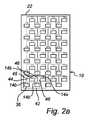
本発明の別の実施例に従った照明装置10が、図2a及び図2bに関連して、ここで説明されよう。図2a、図2bの装置は、図1a、図1bの装置と比較して、異なるLED接点の選択、及び電極の構造を持つ。すなわち、図2a、図2bの装置は、4個の連続なLEDの並列な一群42を有する。各一群又は一連のLED 42は、上部接点及び下部接点を有する1個のLED 14aと、上部接点のみを有する3個のLED 14bとを有している。絶縁用の切れ込み44が、上部-下部接点をもつ1個のLED 14aを上部接点のみをもつLED 14bと直列に接続するため、及び装置の他のLED 14から絶縁するために、上部電極22に供される。従って、絶縁された、電気的に導通のある「チャネル」46が、一連のLED 42の間に供される。下部接点があるので、上部-下部接点をもつLED 14aは、照明装置の他の上部-下部接点をもつLEDと並列に、依然として接続されている。また、直列接続された最後のLED 14bは、上部電極22を介して他のLEDのグループと並列に接続されている。最後に、図2bで見られるように、短絡を回避するために、下部電極24は、上部接点をもつLED 14bを絶縁するために、上部接点をもつLED 14bと共に並べられた最適な大きさの絶縁パッチ48を具備している。代替的には、LED 14bの下部が絶縁されていてもよく、この場合、下部電極24にはパッチは必要とされない。 A
本発明によるLEDべースの照明装置10のアプリケーションは、オフィス照明、又は雰囲気照明、又は装飾的な照明などの屋内の照明、建物の照明などの屋外の照明、照明によるサイン、等々を含む。 Applications of the LED-based
当業者は、本発明は、上で説明された好ましい実施例に決して限定されることはないと理解している。見方を変えれば、多くの修正及び変更が、添付の請求項の範囲内で可能である。例えば、種々異なる接点(例えば、上部及び下部、下部のみ、上部のみ)を有するLEDの多くの他の組合せ、及び電極の一方又は両方の構造化(加工)が、LEDの所望の結合を実現するために可能である。また、LEDの他の配置及び他のデザイン、並びに他の外部結合部構造が想定される。例えば、側面発光LEDは、複数の異なる方向に光を発することができ、外部結合構造部は、導光板からの光を複数の方向に導くのと同様、複数の方向から来る光を反射するために配置されることができる。 The person skilled in the art realizes that the present invention by no means is limited to the preferred embodiments described above. In other words, many modifications and changes are possible within the scope of the appended claims. For example, many other combinations of LEDs with different contacts (eg, top and bottom, bottom only, top only) and structuring (machining) one or both of the electrodes will achieve the desired coupling of the LEDs Is possible for. Also other arrangements and other designs of LEDs and other external coupling structures are envisaged. For example, side-emitting LEDs can emit light in multiple different directions, and the external coupling structure reflects light coming from multiple directions, as well as directing light from the light guide plate in multiple directions Can be arranged.
Claims (4)
Translated fromJapanese前記導光板へと光を発するための複数のLEDと、
前記導光板から光を抽出する複数の反射体と、
前記複数のLEDに接続される第1の電極及び第2の電極とを有する照明装置であって、
前記第1の電極が、前記導光板の一方面に沿って配置され、前記第2の電極が、前記導光板の他方面に沿って配置され、前記複数のLED及び前記複数の反射体が、それぞれ、前記導光板の貫通穴内に配置され、前記第1の電極が、各反射体に対応して設けられた穴を有し、これにより、前記LEDにより発された光が前記導光板及び前記反射体を介して前記第1の電極の前記穴から出るように構成される、照明装置。A light guide plate;
A plurality of LEDs for emitting light to the light guide plate;
A plurality ofreflectors for extracting light from the light guide plate;
Alighting devicethat having a first electrode and a secondelectrode connected to theplurality of LED,
Said first electrodeis disposedalong onesurface of the light guide plate, the second electrodeis disposedalong the othersurface of the light guideplate, wherein the plurality of LED and the plurality of reflectors is, Respectively disposed in the through hole of the light guide plate, the first electrode has a hole provided corresponding to each reflector, whereby light emitted by the LED is transmitted to the light guide plate and the light guide plate. A lighting deviceconfigured to exit from the hole of the first electrode via a reflector .
Applications Claiming Priority (5)
| Application Number | Priority Date | Filing Date | Title |
|---|---|---|---|
| EP06122321 | 2006-10-16 | ||
| EP06122321.0 | 2006-10-16 | ||
| EP06123127.0 | 2006-10-30 | ||
| EP06123127 | 2006-10-30 | ||
| PCT/IB2007/054170WO2008047286A2 (en) | 2006-10-16 | 2007-10-12 | Light emitting diode lighting device |
Publications (2)
| Publication Number | Publication Date |
|---|---|
| JP2010507192A JP2010507192A (en) | 2010-03-04 |
| JP5220753B2true JP5220753B2 (en) | 2013-06-26 |
Family
ID=39149299
Family Applications (1)
| Application Number | Title | Priority Date | Filing Date |
|---|---|---|---|
| JP2009531973AActiveJP5220753B2 (en) | 2006-10-16 | 2007-10-12 | Light emitting diode lighting device |
Country Status (7)
| Country | Link |
|---|---|
| US (1) | US7980747B2 (en) |
| EP (1) | EP2082167B1 (en) |
| JP (1) | JP5220753B2 (en) |
| BR (1) | BRPI0717787B1 (en) |
| ES (1) | ES2624591T3 (en) |
| PL (1) | PL2082167T3 (en) |
| WO (1) | WO2008047286A2 (en) |
Cited By (1)
| Publication number | Priority date | Publication date | Assignee | Title |
|---|---|---|---|---|
| US8792545B2 (en) | 1999-01-19 | 2014-07-29 | Interdigital Technology Corporation | Balancing amplitude and phase |
Families Citing this family (16)
| Publication number | Priority date | Publication date | Assignee | Title |
|---|---|---|---|---|
| CN101529156B (en)* | 2006-10-16 | 2012-03-21 | 皇家飞利浦电子股份有限公司 | Lighting device |
| GB2464916B (en) | 2008-10-21 | 2013-07-31 | Iti Scotland Ltd | Light Guides |
| EP2404202B1 (en) | 2009-03-05 | 2016-08-10 | Design LED Products Limited | Light guides |
| EP2404201B1 (en)* | 2009-03-05 | 2016-07-27 | Design LED Products Limited | Light guides |
| US20110038141A1 (en)* | 2009-08-11 | 2011-02-17 | Martin David Tillin | Lateral emission led backlight for lcd |
| DE102009051188A1 (en)* | 2009-10-29 | 2011-05-19 | Siemens Aktiengesellschaft | Light signal transmitter and light receiver for an optical sensor |
| US8646928B2 (en)* | 2010-12-31 | 2014-02-11 | Global Lighting Technologies, Inc. | Backlight module and liquid crystal display apparatus |
| US9618671B2 (en) | 2011-03-26 | 2017-04-11 | Schott Ag | LED lighting device |
| AT511756B1 (en)* | 2011-08-01 | 2013-06-15 | Sattler Erich Ernst | SIGN |
| US8307547B1 (en) | 2012-01-16 | 2012-11-13 | Indak Manufacturing Corp. | Method of manufacturing a circuit board with light emitting diodes |
| TWI476350B (en)* | 2012-03-21 | 2015-03-11 | Young Lighting Technology Inc | Light source module |
| US8974077B2 (en) | 2012-07-30 | 2015-03-10 | Ultravision Technologies, Llc | Heat sink for LED light source |
| US9271408B2 (en)* | 2013-03-27 | 2016-02-23 | Tdk Corporation | Power supply device |
| US9195281B2 (en) | 2013-12-31 | 2015-11-24 | Ultravision Technologies, Llc | System and method for a modular multi-panel display |
| USD774474S1 (en)* | 2015-02-04 | 2016-12-20 | Xiaofeng Li | Light emitting diodes on a printed circuit board |
| KR102833382B1 (en) | 2018-08-28 | 2025-07-14 | 삼성디스플레이 주식회사 | Backlight unit and display device having the same |
Family Cites Families (14)
| Publication number | Priority date | Publication date | Assignee | Title |
|---|---|---|---|---|
| JPH1062786A (en) | 1996-08-22 | 1998-03-06 | Omron Corp | Light guide device, liquid crystal display, and electronic equipment |
| JP3409666B2 (en)* | 1996-12-02 | 2003-05-26 | 日亜化学工業株式会社 | Surface light emitting device and display device using the same |
| JP4107086B2 (en)* | 1996-12-02 | 2008-06-25 | 日亜化学工業株式会社 | Planar light emitting device and display device using the same |
| JP4747254B2 (en) | 2001-09-13 | 2011-08-17 | Jnc株式会社 | Liquid crystal compound, liquid crystal composition, and liquid crystal display device |
| TWI308239B (en)* | 2002-10-25 | 2009-04-01 | Toppoly Optoelectronics Corp | Light module and flat panel display including the light module |
| JP4161713B2 (en) | 2002-12-27 | 2008-10-08 | カシオ計算機株式会社 | Surface lighting device |
| JP4325207B2 (en)* | 2003-02-06 | 2009-09-02 | 日亜化学工業株式会社 | Surface emitting device |
| US7374327B2 (en)* | 2004-03-31 | 2008-05-20 | Schexnaider Craig J | Light panel illuminated by light emitting diodes |
| JP2005327569A (en)* | 2004-05-13 | 2005-11-24 | Harison Toshiba Lighting Corp | Lighting device |
| TWM263518U (en)* | 2004-07-06 | 2005-05-01 | Au Optronics Corp | Backlight module |
| US7168842B2 (en)* | 2004-12-01 | 2007-01-30 | Au Optronics Corporation | Light emitting diode backlight package |
| WO2006137660A2 (en) | 2005-06-22 | 2006-12-28 | Fawoo Technology Co., Ltd. | Back light unit |
| KR100540055B1 (en)* | 2005-06-22 | 2006-01-11 | 화우테크놀러지 주식회사 | Backlight unit with heat radiation frame for light source |
| JP4329781B2 (en)* | 2006-05-12 | 2009-09-09 | エプソンイメージングデバイス株式会社 | Illumination device and liquid crystal device |
- 2007
- 2007-10-12JPJP2009531973Apatent/JP5220753B2/enactiveActive
- 2007-10-12PLPL07826733Tpatent/PL2082167T3/enunknown
- 2007-10-12EPEP07826733.3Apatent/EP2082167B1/enactiveActive
- 2007-10-12ESES07826733.3Tpatent/ES2624591T3/enactiveActive
- 2007-10-12BRBRPI0717787-9Apatent/BRPI0717787B1/ennot_activeIP Right Cessation
- 2007-10-12WOPCT/IB2007/054170patent/WO2008047286A2/enactiveApplication Filing
- 2007-10-12USUS12/439,791patent/US7980747B2/enactiveActive
Cited By (1)
| Publication number | Priority date | Publication date | Assignee | Title |
|---|---|---|---|---|
| US8792545B2 (en) | 1999-01-19 | 2014-07-29 | Interdigital Technology Corporation | Balancing amplitude and phase |
Also Published As
| Publication number | Publication date |
|---|---|
| WO2008047286A2 (en) | 2008-04-24 |
| ES2624591T3 (en) | 2017-07-17 |
| BRPI0717787B1 (en) | 2018-06-26 |
| US7980747B2 (en) | 2011-07-19 |
| EP2082167A2 (en) | 2009-07-29 |
| US20100053955A1 (en) | 2010-03-04 |
| BRPI0717787A2 (en) | 2013-10-29 |
| WO2008047286A3 (en) | 2008-06-12 |
| PL2082167T3 (en) | 2017-08-31 |
| JP2010507192A (en) | 2010-03-04 |
| EP2082167B1 (en) | 2017-02-22 |
Similar Documents
| Publication | Publication Date | Title |
|---|---|---|
| JP5220753B2 (en) | Light emitting diode lighting device | |
| CN101529157B (en) | Light emitting diode lighting device | |
| US8573823B2 (en) | Solid-state luminaire | |
| KR100883346B1 (en) | Panel type LED lighting device | |
| JP5123862B2 (en) | Two-dimensional lighting device | |
| TWI461629B (en) | Illuminating apparatus and illuminating module thereof | |
| JP2010135309A (en) | Led lamp | |
| JP2007073968A (en) | Thin light source using flexible circuit support | |
| CN101660715A (en) | Light-emitting diode lamp | |
| US9605830B1 (en) | Systems, methods and devices for an LED lighting module with a light transmissive cover | |
| JP2012244018A (en) | Light-emitting module and illumination apparatus | |
| JP2011014535A (en) | Lighting equipment | |
| CN106716010A (en) | Led lighting device | |
| JP2005158958A (en) | Light emitting apparatus | |
| JP2012243393A (en) | Lighting fixture | |
| JP2009104913A (en) | Lighting fixtures and emergency lights | |
| JP2012175013A (en) | Light-emitting device and illumination apparatus | |
| JP2007066906A (en) | Light emitting diode bulb | |
| JP2013045604A (en) | Lighting fixture | |
| KR101032606B1 (en) | LED lighting module | |
| JP6316045B2 (en) | lighting equipment | |
| US20110285268A1 (en) | Light-emitting device | |
| KR101131398B1 (en) | LED light condenser | |
| JP2009049386A (en) | Illumination light source and illumination device | |
| CN103912804A (en) | Large angle light emitting diode (LED) lamp |
Legal Events
| Date | Code | Title | Description |
|---|---|---|---|
| A621 | Written request for application examination | Free format text:JAPANESE INTERMEDIATE CODE: A621 Effective date:20101008 | |
| A131 | Notification of reasons for refusal | Free format text:JAPANESE INTERMEDIATE CODE: A131 Effective date:20120605 | |
| A521 | Request for written amendment filed | Free format text:JAPANESE INTERMEDIATE CODE: A523 Effective date:20120905 | |
| TRDD | Decision of grant or rejection written | ||
| A01 | Written decision to grant a patent or to grant a registration (utility model) | Free format text:JAPANESE INTERMEDIATE CODE: A01 Effective date:20130205 | |
| A61 | First payment of annual fees (during grant procedure) | Free format text:JAPANESE INTERMEDIATE CODE: A61 Effective date:20130306 | |
| FPAY | Renewal fee payment (event date is renewal date of database) | Free format text:PAYMENT UNTIL: 20160315 Year of fee payment:3 | |
| R150 | Certificate of patent or registration of utility model | Free format text:JAPANESE INTERMEDIATE CODE: R150 Ref document number:5220753 Country of ref document:JP Free format text:JAPANESE INTERMEDIATE CODE: R150 | |
| FPAY | Renewal fee payment (event date is renewal date of database) | Free format text:PAYMENT UNTIL: 20160315 Year of fee payment:3 | |
| R250 | Receipt of annual fees | Free format text:JAPANESE INTERMEDIATE CODE: R250 | |
| S533 | Written request for registration of change of name | Free format text:JAPANESE INTERMEDIATE CODE: R313533 | |
| R350 | Written notification of registration of transfer | Free format text:JAPANESE INTERMEDIATE CODE: R350 | |
| S111 | Request for change of ownership or part of ownership | Free format text:JAPANESE INTERMEDIATE CODE: R313113 | |
| R350 | Written notification of registration of transfer | Free format text:JAPANESE INTERMEDIATE CODE: R350 | |
| R250 | Receipt of annual fees | Free format text:JAPANESE INTERMEDIATE CODE: R250 | |
| R250 | Receipt of annual fees | Free format text:JAPANESE INTERMEDIATE CODE: R250 | |
| R250 | Receipt of annual fees | Free format text:JAPANESE INTERMEDIATE CODE: R250 | |
| S531 | Written request for registration of change of domicile | Free format text:JAPANESE INTERMEDIATE CODE: R313531 | |
| S533 | Written request for registration of change of name | Free format text:JAPANESE INTERMEDIATE CODE: R313533 | |
| R350 | Written notification of registration of transfer | Free format text:JAPANESE INTERMEDIATE CODE: R350 | |
| R250 | Receipt of annual fees | Free format text:JAPANESE INTERMEDIATE CODE: R250 | |
| R250 | Receipt of annual fees | Free format text:JAPANESE INTERMEDIATE CODE: R250 | |
| R250 | Receipt of annual fees | Free format text:JAPANESE INTERMEDIATE CODE: R250 | |
| R250 | Receipt of annual fees | Free format text:JAPANESE INTERMEDIATE CODE: R250 | |
| R250 | Receipt of annual fees | Free format text:JAPANESE INTERMEDIATE CODE: R250 | |
| R250 | Receipt of annual fees | Free format text:JAPANESE INTERMEDIATE CODE: R250 |