JP5217494B2 - Artificial medium, method for manufacturing the same, and antenna device - Google Patents
Artificial medium, method for manufacturing the same, and antenna deviceDownload PDFInfo
- Publication number
- JP5217494B2 JP5217494B2JP2008045071AJP2008045071AJP5217494B2JP 5217494 B2JP5217494 B2JP 5217494B2JP 2008045071 AJP2008045071 AJP 2008045071AJP 2008045071 AJP2008045071 AJP 2008045071AJP 5217494 B2JP5217494 B2JP 5217494B2
- Authority
- JP
- Japan
- Prior art keywords
- conductive
- artificial medium
- elements
- linear conductor
- dielectric
- Prior art date
- Legal status (The legal status is an assumption and is not a legal conclusion. Google has not performed a legal analysis and makes no representation as to the accuracy of the status listed.)
- Expired - Fee Related
Links
Images


Classifications
- H—ELECTRICITY
- H01—ELECTRIC ELEMENTS
- H01Q—ANTENNAS, i.e. RADIO AERIALS
- H01Q21/00—Antenna arrays or systems
- H01Q21/06—Arrays of individually energised antenna units similarly polarised and spaced apart
- H01Q21/061—Two dimensional planar arrays
- H01Q21/065—Patch antenna array
- H—ELECTRICITY
- H01—ELECTRIC ELEMENTS
- H01P—WAVEGUIDES; RESONATORS, LINES, OR OTHER DEVICES OF THE WAVEGUIDE TYPE
- H01P3/00—Waveguides; Transmission lines of the waveguide type
- H01P3/02—Waveguides; Transmission lines of the waveguide type with two longitudinal conductors
- H01P3/08—Microstrips; Strip lines
- H01P3/088—Stacked transmission lines
- H—ELECTRICITY
- H01—ELECTRIC ELEMENTS
- H01Q—ANTENNAS, i.e. RADIO AERIALS
- H01Q15/00—Devices for reflection, refraction, diffraction or polarisation of waves radiated from an antenna, e.g. quasi-optical devices
- H01Q15/0006—Devices acting selectively as reflecting surface, as diffracting or as refracting device, e.g. frequency filtering or angular spatial filtering devices
- H01Q15/0013—Devices acting selectively as reflecting surface, as diffracting or as refracting device, e.g. frequency filtering or angular spatial filtering devices said selective devices working as frequency-selective reflecting surfaces, e.g. FSS, dichroic plates, surfaces being partly transmissive and reflective
- H01Q15/0026—Devices acting selectively as reflecting surface, as diffracting or as refracting device, e.g. frequency filtering or angular spatial filtering devices said selective devices working as frequency-selective reflecting surfaces, e.g. FSS, dichroic plates, surfaces being partly transmissive and reflective said selective devices having a stacked geometry or having multiple layers
- H—ELECTRICITY
- H01—ELECTRIC ELEMENTS
- H01Q—ANTENNAS, i.e. RADIO AERIALS
- H01Q15/00—Devices for reflection, refraction, diffraction or polarisation of waves radiated from an antenna, e.g. quasi-optical devices
- H01Q15/14—Reflecting surfaces; Equivalent structures
- H01Q15/141—Apparatus or processes specially adapted for manufacturing reflecting surfaces
- H01Q15/142—Apparatus or processes specially adapted for manufacturing reflecting surfaces using insulating material for supporting the reflecting surface
- H—ELECTRICITY
- H01—ELECTRIC ELEMENTS
- H01Q—ANTENNAS, i.e. RADIO AERIALS
- H01Q21/00—Antenna arrays or systems
- H01Q21/06—Arrays of individually energised antenna units similarly polarised and spaced apart
- H01Q21/08—Arrays of individually energised antenna units similarly polarised and spaced apart the units being spaced along or adjacent to a rectilinear path
- H—ELECTRICITY
- H01—ELECTRIC ELEMENTS
- H01Q—ANTENNAS, i.e. RADIO AERIALS
- H01Q9/00—Electrically-short antennas having dimensions not more than twice the operating wavelength and consisting of conductive active radiating elements
- H01Q9/04—Resonant antennas
- H01Q9/16—Resonant antennas with feed intermediate between the extremities of the antenna, e.g. centre-fed dipole
- H01Q9/28—Conical, cylindrical, cage, strip, gauze, or like elements having an extended radiating surface; Elements comprising two conical surfaces having collinear axes and adjacent apices and fed by two-conductor transmission lines
- H01Q9/285—Planar dipole
- H—ELECTRICITY
- H01—ELECTRIC ELEMENTS
- H01Q—ANTENNAS, i.e. RADIO AERIALS
- H01Q9/00—Electrically-short antennas having dimensions not more than twice the operating wavelength and consisting of conductive active radiating elements
- H01Q9/04—Resonant antennas
- H01Q9/30—Resonant antennas with feed to end of elongated active element, e.g. unipole
- H01Q9/40—Element having extended radiating surface
- Y—GENERAL TAGGING OF NEW TECHNOLOGICAL DEVELOPMENTS; GENERAL TAGGING OF CROSS-SECTIONAL TECHNOLOGIES SPANNING OVER SEVERAL SECTIONS OF THE IPC; TECHNICAL SUBJECTS COVERED BY FORMER USPC CROSS-REFERENCE ART COLLECTIONS [XRACs] AND DIGESTS
- Y10—TECHNICAL SUBJECTS COVERED BY FORMER USPC
- Y10T—TECHNICAL SUBJECTS COVERED BY FORMER US CLASSIFICATION
- Y10T156/00—Adhesive bonding and miscellaneous chemical manufacture
- Y10T156/10—Methods of surface bonding and/or assembly therefor
Landscapes
- Engineering & Computer Science (AREA)
- Manufacturing & Machinery (AREA)
- Physics & Mathematics (AREA)
- Electromagnetism (AREA)
- Aerials With Secondary Devices (AREA)
- Waveguide Connection Structure (AREA)
- Details Of Aerials (AREA)
- Variable-Direction Aerials And Aerial Arrays (AREA)
Abstract
Description
Translated fromJapanese本発明は、媒質に関し、特にメタマテリアルとも呼ばれる人工媒質に関する。また、本発明は、そのような人工媒質の製造方法およびそのような人工媒質を用いたアンテナ装置に関する。 The present invention relates to a medium, and more particularly to an artificial medium also called a metamaterial. The present invention also relates to a method for manufacturing such an artificial medium and an antenna device using such an artificial medium.
金属等のインクルージョンパターンを、微細なレベルで高精度に配列させることにより、自然には得られない材料特性(実効比誘電率、実効比透磁率等)を発現させた媒質、いわゆる人工媒質は、高周波用アンテナ、超小型通信用の共振器、発信器およびサブ波長用焦点レンズなど、様々な分野での適用が期待されている。 By arranging the inclusion pattern such as metal with high precision at a fine level, a medium that expresses material properties (effective relative permittivity, effective relative permeability, etc.) that cannot be obtained naturally, so-called artificial media, Applications in various fields such as a high-frequency antenna, a resonator for ultra-small communication, a transmitter, and a sub-wavelength focus lens are expected.
このような人工媒質の典型的な構成の一例を図1に示す。人工媒質1は、図1に示すように、長さW、幅Dおよび厚さTを有する。媒質1は、厚さが実質的にtの誘電体層2を媒質1の長手方向(図のX方向)に多数積層させることにより構成される。また、誘電体層2は、導電面4(図のYZ平面)に、インクルージョンとしてのスプリットリング3の配列パターンを有する。各スプリットリング3は、図の手前側(Y方向の負側)に分離部6を有する。 An example of a typical configuration of such an artificial medium is shown in FIG. As shown in FIG. 1, the
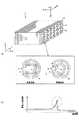
次に、このように構成された媒質の特性を図2を参照して説明する。図2は、従来の人工媒質において、実効比透磁率の上昇が生じる原理を示したものである。 Next, the characteristics of the medium configured as described above will be described with reference to FIG. FIG. 2 shows the principle of increase in effective relative permeability in a conventional artificial medium.
前述の人工媒質1に、Z方向に伝播する電磁波5(電界の向きEは、Y方向、磁界の向きHは、X方向)を入射させた場合、低周波数側では、スプリットリング3の外周側と内周側で逆向きの電流が流れる。すなわち、スプリットリング3の外周側では、時計回りに電流の流れ8が生じ、内周側では、反時計回りに電流の流れ9が生じる。従って、この場合、両者の電流によって生じる磁界は、互いに相殺され、全体として実効比透磁率の増大は生じない。しかしながら、周波数が次第に高くなると、ある周波数(共振周波数)では、スプリットリング3に流れる電流が分離部6を飛び越え、分離部6には、変位電流7が生じるようになる。またこれにより、スプリットリング3の外周側および内周側において、それぞれ同じ反時計回り方向に電流の流れ8および9が生じるようになり、スプリットリング3に流れる電流がループ電流となる。このようなループ電流の発生の結果、人工媒質を通る磁束が強まり、人工媒質の実効比透磁率が見かけ上向上する。 When the
以上のような人工媒質の実効比透磁率の周波数に対する変化の影響は、図2の下のグラフのように表される。このグラフにおいて、丸で囲った周波数領域では、前述の原理によって、実効比透磁率の著しい増大が得られることになる。 The influence of the change on the frequency of the effective relative permeability of the artificial medium as described above is expressed as a lower graph in FIG. In this graph, in the circled frequency region, a significant increase in effective relative permeability is obtained by the above-described principle.
このような原理を利用した人工媒質については、スプリットリングまたは螺旋コイルのようなインクルージョンの形状および配列パターン等によって、様々な特性を発現させることができるため、これまでに多くの提案が示されている(例えば、特許文献1、2、非特許文献1)。
ところで、従来の人工媒質においては、前述のような実効比透磁率の増大効果を得るためには、インクルージョンの導電面4が電磁波5の入射方向に対して平行に配設されるように、媒質1を形成する必要がある。これは、前述のような電流の流れ方向の周波数依存性を利用して人工媒質の実効比透磁率の向上を発現させるためには、入射される電磁波5の磁界の振幅方向Hを横切るように、インクルージョンの導電面4を配置させなければならないからである。電磁波5の磁界方向Hと導電面4の間には、このような相対関係が必要であるため、従来の人工媒質では、人工媒質を構成する際に、完成後の人工媒質の長さ方向(図1のX方向)に沿って、誘電体層2が積層される。従って、通常の場合、人工媒質の受信面(すなわち、電磁波の入射方向と垂直な面(XY平面))と、誘電体層2の導電面4の方向が一致することはない。 By the way, in the conventional artificial medium, in order to obtain the effect of increasing the effective relative permeability as described above, the medium is so arranged that the
しかしながら、この場合、誘電体層を積層して、長さWの人工媒質1を得るためには、極めて多くの枚数分の誘電体層2を積層させる必要がある。例えば、厚さが1mm程度の誘電体層では、長さWが10cmの人工媒質を得るためには、100枚もの誘電体層を積層させなければならない。従って、人工媒質の製造コストが極めて高くなるという問題が生じる。 However, in this case, in order to obtain the
また、人工媒質を構成する各誘電体層2には、少なくとも1個のインクルージョンを配置させる必要があるため、人工媒質1の厚さT(図1のZ方向の長さ)は、当然のことながら、このインクルージョンの寸法(通常マイクロ波帯においては、5〜20mm程度)以下に薄くすることはできない。従って、従来のような構成では、人工媒質を小型化(特に薄型化)させることは、極めて難しいという問題があった。 Further, since it is necessary to dispose at least one inclusion in each
本発明は、このような問題に鑑みなされたものであり、安価に製造することが可能であり、かつ小型化の可能な人工媒質、そのような人工媒質の製造方法、およびそのような人工媒質を用いたアンテナ装置を提供することを目的とする。 The present invention has been made in view of such problems, and can be manufactured at low cost, and can be miniaturized, a method for manufacturing such an artificial medium, and such an artificial medium. An object of the present invention is to provide an antenna device using the antenna.
本発明では、導電性素子が2次元周期配列的に配置された導電面が、厚さ方向に2面以上設置された人工媒質であって、前記厚さ方向と平行に伝播する電磁波が入射された際に、該電磁波により励起される電流が、動作周波数において増大するとともに、前記厚さ方向と平行な面内に電流のループが形成されることを特徴とする人工媒質が提供される。 In the present invention, the conductive surface in which the conductive elements are arranged in a two-dimensional periodic array is an artificial medium in which two or more surfaces are installed in the thickness direction, and an electromagnetic wave propagating in parallel with the thickness direction is incident. In this case, an artificial medium is provided in which a current excited by the electromagnetic wave increases at an operating frequency and a current loop is formed in a plane parallel to the thickness direction.
また、本発明による人工媒質では、各導電面の間には、誘電体層が介在され、各誘電体層を介して導電性素子が厚さ方向に相互に対向する領域に、電流のループが形成されても良い。 In the artificial medium according to the present invention, a dielectric layer is interposed between the conductive surfaces, and current loops are formed in regions where the conductive elements face each other in the thickness direction via the dielectric layers. It may be formed.
また本発明による人工媒質では、各導電面は、相互に分離した複数の導電性素子からなる実質的に同一の配列パターンを有し、各導電性素子は、前記厚さ方向に沿って位置が揃っていても良い。特に、各導電性素子の形状および寸法は、実質的に同一であっても良い。 Further, in the artificial medium according to the present invention, each conductive surface has a substantially identical arrangement pattern composed of a plurality of conductive elements separated from each other, and each conductive element is positioned along the thickness direction. You may have it. In particular, the shape and dimensions of each conductive element may be substantially the same.
また本発明による人工媒質では、前記誘電体層の内部には、該誘電体層の厚みの中心部近傍に、相互に平行な複数の第1の直線状導体素子が配置され、
該第1の直線状導体素子は、前記誘電体層の一端から他端に向かって、実質的に直線状に延伸し、
前記導電面と垂直な方向から見た場合、前記第1の直線状導体素子の少なくとも一つは、少なくともいずれかの導電性素子と重なるように配置されても良い。In the artificial medium according to the present invention, a plurality of first linear conductor elements parallel to each other are arranged in the vicinity of the center portion of the thickness of the dielectric layer inside the dielectric layer,
The first linear conductor element extends substantially linearly from one end of the dielectric layer to the other end,
When viewed from a direction perpendicular to the conductive surface, at least one of the first linear conductor elements may be disposed so as to overlap at least one of the conductive elements.
また本発明による人工媒質では、さらに、前記複数の第1の直線状導体素子と同等の深さ位置に、相互に平行な複数の第2の直線状導体素子を有し、
該複数の第2の直線状導体素子は、前記第1の直線状導体素子とは異なる方向に沿って、前記誘電体層の一端から他端まで、実質的に直線状に延伸し、
前記複数の第2の直線状導体素子は、前記導電面と垂直な方向から見た場合、少なくとも一部は、少なくともいずれかの導電性素子と重なるように配置されても良い。The artificial medium according to the present invention further includes a plurality of second linear conductor elements parallel to each other at a depth position equivalent to that of the plurality of first linear conductor elements,
The plurality of second linear conductor elements extend substantially linearly from one end of the dielectric layer to the other end along a direction different from the first linear conductor element,
The plurality of second linear conductor elements may be arranged so that at least a part thereof overlaps at least one of the conductive elements when viewed from a direction perpendicular to the conductive surface.
ここで、前記前記第1および第2の直線状導体素子は、前記導電面と垂直な方向から見た場合、前記第1の直線状導体素子と第2の直線状導体素子の交点がいずれかの導電性素子の領域に収まるように配置されも良い。 Here, the first and second linear conductor elements are either intersections of the first linear conductor element and the second linear conductor element when viewed from a direction perpendicular to the conductive surface. It may be arranged so as to fit in the region of the conductive element.
あるいは、これとは別に、またはこれに加えて、前記導電性素子は、前記導電面に行および列に沿って、それぞれ一定のピッチで配列され、
前記導電面と垂直な方向から見た場合、第1の直線状導体素子の少なくとも一つは、一つの列を構成する各導電性素子と重なるように配置され、
および/または前記導電面と垂直な方向から見た場合、第2の直線状導体素子の少なくとも一つは、一つの行を構成する各導電性素子と重なるように配置されても良い。Alternatively, or in addition, the conductive elements are arranged on the conductive surface along rows and columns, respectively, at a constant pitch,
When viewed from a direction perpendicular to the conductive surface, at least one of the first linear conductor elements is arranged so as to overlap each conductive element constituting one row,
When viewed from a direction perpendicular to the conductive surface, at least one of the second linear conductor elements may be disposed so as to overlap with each conductive element constituting one row.
また、前記導電性素子は、前記導電面に行および列に沿って、それぞれ一定のピッチで配列され、
前記第1の直線状導体素子は、前記導電性素子の列のピッチと実質的に等しいピッチで配置され、
および/または第2の直線状導体素子は、前記導電性素子の行のピッチと実質的に等しいピッチで配置されても良い。In addition, the conductive elements are arranged at a certain pitch along rows and columns on the conductive surface,
The first linear conductor elements are arranged at a pitch substantially equal to the pitch of the row of conductive elements;
And / or the second linear conductor elements may be arranged at a pitch substantially equal to the pitch of the row of conductive elements.
特に、前記導電面と垂直な方向から見た場合、前記導電性素子は、第1および第2の直線状導体素子の全ての交点に配置され、かつ前記交点を除く位置には配置されていなくても良い。 In particular, when viewed from a direction perpendicular to the conductive surface, the conductive element is disposed at all intersections of the first and second linear conductor elements, and is not disposed at a position other than the intersection. May be.
あるいは、前記導電性素子は、前記導電面に行および列に沿って、それぞれ一定のピッチで配列され、
前記第1の直線状導体素子は、前記導電性素子の列のピッチの実質的に2倍のピッチで配置され、
および/または第2の直線状導体素子は、前記導電性素子の行のピッチの実質的に2倍のピッチで配置されても良い。Alternatively, the conductive elements are arranged on the conductive surface along rows and columns, respectively, at a constant pitch,
The first linear conductor elements are arranged at a pitch substantially twice the pitch of the row of conductive elements;
And / or the second linear conductor elements may be arranged at a pitch substantially twice the pitch of the row of conductive elements.
また前述のような、前記複数の第1の直線状導体素子と同等の深さ位置に、相互に平行な複数の第2の直線状導体素子を有する人工媒質において、
前記導電性素子は、前記導電面に行および列に沿って、それぞれ一定のピッチで配列され、
前記複数の第1の直線状導体素子および第2の直線状導体素子は、実質的に同一の間隔で配置され、
前記第1の直線状導体素子は、前記導電性素子の列の方向に対して時計回りに45゜回転した方向に延伸するように配置され、
前記第1の直線状導体素子は、前記導電性素子の列の方向に対して反時計回りに45゜回転した方向に延伸するように配置されても良い。In the artificial medium having a plurality of second linear conductor elements parallel to each other at the same depth as the plurality of first linear conductor elements as described above,
The conductive elements are arranged at a constant pitch along rows and columns on the conductive surface, respectively.
The plurality of first linear conductor elements and the second linear conductor elements are disposed at substantially the same interval,
The first linear conductor elements are arranged to extend in a direction rotated 45 ° clockwise relative to the direction of the row of conductive elements;
The first linear conductor element may be arranged to extend in a direction rotated 45 ° counterclockwise with respect to the direction of the row of the conductive elements.
特に、前記導電性素子は、前記導電面と垂直な方向から見た場合、第1および第2の直線状導体素子の全ての交点に配置され、かつ前記交点を除く位置には配置されていなくても良い。 In particular, the conductive element is disposed at all intersections of the first and second linear conductor elements when viewed from a direction perpendicular to the conductive surface, and is not disposed at a position other than the intersection. May be.
なおこれらの人工媒質において、前記複数の導電性素子は、実質的に正方形の形状を有しても良い。 In these artificial media, the plurality of conductive elements may have a substantially square shape.
また、前記第1の直線状導体素子および/または第2の直線状導体素子の線幅は、前記導電性素子の同方向における幅よりも狭くても広くても良い。ここで、「導電性素子の同方向における幅」とは、直線状導体素子の線幅の方向と等しい方向で見た、導電性素子の長さを意味することに留意する必要がある。例えば、導電性素子の形状が円の場合、「導電性素子の同方向における幅」は、その直径となる。また、導電性素子の形状が矩形状であって、その長辺が直線状導体素子の線幅の方向と平行となるように配置されている場合、「導電性素子の同方向における幅」は、長辺の長さとなり、その短辺が直線状導体素子の線幅の方向と平行となるように配置されている場合、「導電性素子の同方向における幅」は、短辺の長さとなり、その対角線が直線状導体素子の線幅の方向と平行となるように配置されている場合、「導電性素子の同方向における幅」は、対角線の長さとなる。 The line width of the first linear conductor element and / or the second linear conductor element may be narrower or wider than the width of the conductive element in the same direction. Here, it should be noted that the “width in the same direction of the conductive element” means the length of the conductive element viewed in the same direction as the line width direction of the linear conductor element. For example, when the shape of the conductive element is a circle, the “width in the same direction of the conductive element” is its diameter. In addition, when the shape of the conductive element is rectangular and the long side thereof is arranged in parallel to the line width direction of the linear conductor element, the “width in the same direction of the conductive element” is , The width of the conductive element in the same direction when the short side is arranged in parallel with the direction of the line width of the linear conductor element is the length of the short side. Thus, when the diagonal line is arranged so as to be parallel to the line width direction of the linear conductor element, the “width in the same direction of the conductive element” is the length of the diagonal line.
また、前記誘電体層は、フッ素樹脂材料で構成されていても良い。 The dielectric layer may be made of a fluororesin material.
さらに、本発明では、導電性素子が配置された導電面を有する誘電体基板を調製するステップと、
前記誘電体基板を厚さ方向に積層して、人工媒質を構成するステップと、
を有する人工媒質を製造する方法であって、
前記誘電体基板を調製するステップは、前記人工媒質に、前記厚さ方向と平行な方向に伝播する電磁波が入射された際に、前記厚さ方向と平行な平面内に電流のループが形成されるように、各誘電体基板に導電性素子を配置するステップを有することを特徴とする人工媒質の製造方法が提供される。Furthermore, in the present invention, a step of preparing a dielectric substrate having a conductive surface on which conductive elements are arranged;
Laminating the dielectric substrate in the thickness direction to form an artificial medium;
A method of manufacturing an artificial medium having
In the step of preparing the dielectric substrate, when an electromagnetic wave propagating in a direction parallel to the thickness direction is incident on the artificial medium, a current loop is formed in a plane parallel to the thickness direction. Thus, a method for manufacturing an artificial medium is provided, which includes a step of disposing a conductive element on each dielectric substrate.
ここで、当該方法では、一つの誘電体基板を介して、前記厚さ方向に相互に対向する導電性素子同士の間に、電流のループが形成されても良い。 Here, in this method, a current loop may be formed between the conductive elements facing each other in the thickness direction via one dielectric substrate.
また当該方法において、前記誘電体基板を厚さ方向に積層して、人工媒質を構成するステップは、導電面に導電性素子が配置された誘電体基板同士の間に、導電性素子を有さない第2の誘電体層を介在させるステップを有しても良い。 In the method, the step of forming the artificial medium by laminating the dielectric substrates in the thickness direction includes conductive elements between the dielectric substrates having conductive elements arranged on conductive surfaces. There may be a step of interposing no second dielectric layer.
さらに、当該方法において、前記誘電体基板を調製するステップは、
前記各誘電体層の厚みの中心部近傍に、直線状導体素子を配置するステップと、
前記誘電体基板を積層した際に、各導電性素子が前記厚さ方向に沿って位置が揃うように、各誘電体基板の導電面に、複数の導電性素子からなる実質的に同一の配列パターンを設置するステップと、
を有し、
前記導電性素子の形状および寸法は、実質的に同一であり、
前記直線状導体素子は、前記誘電体基板の一端から他端に向かって、実質的に直線状に延伸し、
前記導電面と垂直な方向から見た場合、前記直線状導体素子の少なくとも一部は、少なくともいずれかの導電性素子と重なるように配置されても良い。Furthermore, in the method, the step of preparing the dielectric substrate comprises:
Placing a linear conductor element in the vicinity of the center of the thickness of each dielectric layer;
A substantially identical arrangement of a plurality of conductive elements on the conductive surface of each dielectric substrate so that the conductive elements are aligned along the thickness direction when the dielectric substrates are stacked. The step of installing the pattern;
Have
The shape and dimensions of the conductive elements are substantially the same,
The linear conductor element extends substantially linearly from one end of the dielectric substrate to the other end,
When viewed from a direction perpendicular to the conductive surface, at least a part of the linear conductor element may be arranged to overlap at least one of the conductive elements.
さらに、本発明では、
誘電体層と、該誘電体層の表裏面のそれぞれに設置された単一の導電性素子と、を有し、
各導電性素子は、実質的に同一の寸法および形状を有し、前記誘電体層の厚さ方向に沿って位置が揃っており、
前記厚さ方向と平行に伝播する電磁波が入射された際に、前記誘電体層を介して、前記導電性素子が厚さ方向に相互に対向する領域に、電流のループが形成されることを特徴とする人工媒質が提供される。Furthermore, in the present invention,
A dielectric layer, and a single conductive element installed on each of the front and back surfaces of the dielectric layer,
Each conductive element has substantially the same dimensions and shape, and is aligned along the thickness direction of the dielectric layer,
When an electromagnetic wave propagating parallel to the thickness direction is incident, a current loop is formed in a region where the conductive elements face each other in the thickness direction via the dielectric layer. A featured artificial medium is provided.
さらに、本発明では、絶縁体または誘電体で構成された基板の第1の表面に、導体を有するアンテナ素子が配置されたアンテナ装置であって、
前記基板の第1の表面と対向する第2の表面には、人工媒質が配置され、
前記人工媒質は、前述の人工媒質で構成され、前記基板の第1の表面と垂直な方向から見た場合、前記アンテナ素子の少なくとも一部は、前記人工媒質と重なっていることを特徴とするアンテナ装置が提供される。Furthermore, the present invention is an antenna device in which an antenna element having a conductor is disposed on a first surface of a substrate made of an insulator or a dielectric,
An artificial medium is disposed on the second surface opposite to the first surface of the substrate,
The artificial medium is composed of the above-described artificial medium, and when viewed from a direction perpendicular to the first surface of the substrate, at least a part of the antenna element overlaps the artificial medium. An antenna device is provided.
ここで、当該アンテナ装置は、さらに、前記人工媒質の前記基板の第2の表面とは反対の側に、配置された金属板を有しても良い。 Here, the antenna device may further include a metal plate disposed on the side of the artificial medium opposite to the second surface of the substrate.
また当該アンテナ装置において、前記アンテナ素子は、RFIDタグを有しても良い。 In the antenna device, the antenna element may include an RFID tag.
本発明では、安価に製造することが可能であり、かつ小型化の可能な人工媒質、およびそのような人工媒質の製造方法を提供することができる。また本発明では、そのような人工媒質を用いたアンテナ装置を提供することができる。 In the present invention, it is possible to provide an artificial medium that can be manufactured at a low cost and can be reduced in size, and a method for manufacturing such an artificial medium. In the present invention, an antenna device using such an artificial medium can be provided.
以下図面により本発明の形態を説明する。 Hereinafter, embodiments of the present invention will be described with reference to the drawings.
(第1の態様)
図3には、本発明による人工媒質の一構成例の斜視図を示す。また、図4には、本発明による人工媒質を構成する誘電体層の導電面に設置された導電性素子の拡大図を示す。(First aspect)
FIG. 3 shows a perspective view of a configuration example of the artificial medium according to the present invention. FIG. 4 shows an enlarged view of the conductive element installed on the conductive surface of the dielectric layer constituting the artificial medium according to the present invention.
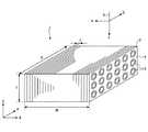
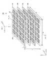
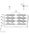
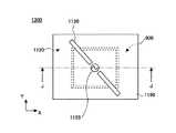
本発明による人工媒質100は、図3に示すように、実質的に、長さW(図3のX方向の長さ)、幅D(図3のY方向の長さ)および厚さt(図3のZ方向の長さ)を有する誘電体層120を、厚さ方向に沿って複数枚積層させることにより構成される。ここで、図3では、説明を明確にするため、人工媒質は、各誘電体層120が分離された分解図として示されているが、実際の本発明による媒質では、各誘電体層は、相互に接触した状態で積層されていることに留意する必要がある。人工媒質100は、長さW、幅Dおよび厚さTを有し、人工媒質100の厚さTは、実質的に誘電体層120の厚さt×積層数で定められる。なお、図3の例では、誘電体層120の積層数は4であるが、これは一例であって、人工媒質100を構成する際の誘電体層120の積層数は、特に限られない。誘電体層120の寸法は、例えば、W=10cm、D=10cm、t=0.2mmである。 As shown in FIG. 3, the
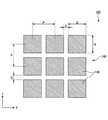
誘電体層120は、図3において、XY平面に延伸する導電面140を有し、この導電面140上には、複数の導電性素子130が配列形成されている。例えば、図3の例では、導電性素子130は、誘電体層120の長さ方向(X方向)に沿って、5個ずつ配列され、誘電体層120の幅方向(Y方向)に沿って、4個ずつ配列され、一つの導電面140には、20個の導電性素子130が配置されている。なお、図3の例では、導電性素子130は、正方形状であるが、導電性素子130は、別の形状、例えば、矩形状、三角形状、多角形状、円状または楕円状であっても良い。 In FIG. 3, the
図4に示すように、誘電体層120の導電面140に形成された正方形状導電性素子130は、一辺の長さがQであり、導電性素子130の配置ピッチ(一つの正方形状導電性素子130の中心と、隣接する正方形状導電性素子130の中心間の距離)は、X方向、Y方向いずれもPであり、導電性素子130間のギャップは、X方向、Y方向いずれもGである。ただしこれらの寸法は、一例であって、配置ピッチおよびギャップは、X方向、Y方向で異なっていても良い。また、導電性素子130の厚さは、特に限られないが、図3の例では、18〜20μmである。また、導電性素子130の材質は、電気伝導性を有する限り、特に限られないが、例えば、銅等の金属で構成される。また、このような導電性素子130の配列パターンは、既存のエッチング技術等を用いることにより、容易に形成することができる。 As shown in FIG. 4, the square
ここで実際の人工媒質では、製造の際に、例えば、複数の誘電体層120を積層後、積層方向(Z方向)に沿って均一な荷重が加えられ、さらにこの状態で熱処理を行うことにより、各誘電体層120が積層方向に接合される。この際に、各誘電体層の導電面140に設置されている導電性素子130は、隣接する誘電体層120の裏面(導電面140とは反対側の表面)に埋没される。従って、実際には、一つの誘電体層120とそれに隣接する誘電体層の界面には、導電性素子による凹凸は生じないことに留意する必要がある。 Here, in the actual artificial medium, for example, after the plurality of
次に、前述のように構成された本発明による人工媒質の特徴的性質について説明する。 Next, the characteristic properties of the artificial medium according to the present invention configured as described above will be described.
最初に図2を参照して示したように、従来の人工媒質では、媒質1は、各誘電体層2の導電面4が電磁波の伝播方向kに対して平行となるように配置される。このように配置しなければ、共振周波数域において、人工媒質に電流ループが形成されないからである。従って、通常の場合、人工媒質の電磁波の伝播方向に対して垂直な面(以下、「受信面」と称する)と、導電面は一致しない。 As shown initially with reference to FIG. 2, in the conventional artificial medium, the
これに対して本発明では、人工媒質100は、入射される電磁波150の伝播方向kに対して垂直となるように、各誘電体層120の導電面140が配置されている(図3参照)。従って、電磁波150を受信する人工媒質の受信面と導電面140とは、一致している。 On the other hand, in the present invention, the
このような配置の場合、人工媒質100を構成する誘電体層120の導電面140自身を受信面として機能させることが可能となるため、前述のような従来の人工媒質1に比べて、誘電体層120の積層数を著しく削減することが可能となる。例えば、長さW=10cm(厚さT=5mm)の人工媒質を構成する場合、厚さtが0.2mmの従来の誘電体層2では、単純計算で誘電体層を500枚積層させる必要があるが、本発明の構成の場合、同じ厚さtを有する誘電体層120では、25枚の積層で済むことになる。従って、媒質の製造コストを有意に抑制することが可能となる。また、従来の人工媒質1は、インクルージョンが電流ループを決定しており、プロセス上、インクルージョンの薄肉化は困難であり、さらに性能の劣化を招くため、媒質のロープロファイル化ができなかった。一方、本発明では、電流ループの薄型化と細密充填に適し、性能を劣化させずに、低コストでロープロファイル化が可能となる。さらに、本発明の媒質では、導電面には、単純な形状(例えば矩形状、円形状など)の導電性素子を配列すれば良く、従来のスプリットリングまたは螺旋コイルのような複雑な形状のインクルージョンは不要である。またこのような導電性素子は、従来のエッチング技術や印刷技術等によって容易に形成することができる。従って、本発明では、人工媒質の導電面の構造が簡略化され、製造が容易になるという効果が得られる。 In the case of such an arrangement, the
次に、本発明による人工媒質100において、電磁波150を受信する人工媒質の受信面と導電面140とを一致させることができる理由を説明する。 Next, the reason why the receiving surface of the artificial medium that receives the
図5および図6には、図3に示した本発明による人工媒質100のA−A断面の拡大図を示す。これらの図には、導電性素子130の上下それぞれの面の側に生じる電流の向きも示されている。特に図5は、低周波数域において人工媒質の導電性素子に生じる電流方向を示したものであり、また図6は、高周波数域において人工媒質の導電性素子に生じる電流方向を示したものである。なお、両図において、電流を表す矢印は、向きが重要であって、その大きさには、特に意味はないことに留意する必要がある。すなわち、矢印の長さは、任意に設定したものであり、実際の各電流の大きさは、同じであっても異なっていても良い。また、これらの図の例では、本発明による人工媒質100は、誘電体層120をZ方向に4層積層することにより構成されている。 5 and 6 are enlarged views of an AA cross section of the
本発明による人工媒質100に、上から下(Z方向の負の向き)に伝播する電磁波150を入射させた場合、低周波数域では、導電性素子130には、図5に示す電流が流れる。すなわち、各導電性素子について見た場合、各導電性素子130の上面側の電流の向き190a、b、cと下面側の電流の向き180a、b、cは、等しくなる。従って、この場合、電流のループは形成されず、実効比透磁率の増大は生じない。これに対して高周波数域では、変位電流170が発生するため、一つの導電性素子について見た場合、導電性素子130のそれぞれの面には、図6に示す方向に電流が流れ、導電性素子130の上面側の電流190a、b、cの向きと下面側の電流180a、b、cの向きは、ちょうど反対になる。これを一つの誘電体層120で見た場合、上側の(すなわち当該誘電体層の導電面140上に配置された)導電性素子130の電流180a、b、cの流れと、下側の(すなわち当該誘電体層の下方に隣接する誘電体層の導電面140上に配置された)導電性素子130の電流190a、b、cの流れと、当該誘電体層内を横断して流れる変位電流170a、b、cの流れとによって、人工媒質100の電磁波150と平行な面内(YZ平面)には、ループ電流Ia、b、cが生じるようになる。このような誘電体層120の積層方向でのループ電流Ia、b、cの発生の結果、磁束が増大し、人工媒質の実効比透磁率は、著しく増大されることになる。 When the
図7には、導電性素子130および誘電体層120に生じる電流の流れと位相の関係をより詳しく示す。電磁波150が誘電体層120の導電面140に対して垂直な方向から入射されると、誘電体層120の厚み部分を介して対向する1組の導電性素子130には、外部電界によって励起された電流185が互いに逆向きに発生する。またこれと同時に、各導電性素子130の端部には、誘電体層の積層方向と平行な方向に、逆向きの変位電流170が生じ、電流185および変位電流170によって、電流ループIが形成される。この状態を位相0゜とする。次に、位相90゜では、1組の導電性素子130間には、前述の変位電流170の位置に、変位電流170と同様の方向の電界171が発生する。さらに、位相180゜では、位相0゜と反対向きに電流185が発生する。また、位相270゜では、位相90゜と反対向きに電界171が発生する。 FIG. 7 shows the relationship between the current flow generated in the
ここで重要なことは、電流ループIによって生じる磁界は、入射される電磁波150の磁界の向きHと同じ方向にあることであり、このため、電流ループIの形成により、磁界を強めることが可能となる。 What is important here is that the magnetic field generated by the current loop I is in the same direction as the magnetic field direction H of the incident
ここで、誘電体層の積層数と特性の関係について説明する。誘電体層を3層以上積層することにより、実効比透磁率の周波数特性を制御することができる。基本的には、対向するどの導電性素子により、電流ループが形成されるかによって、実効比透磁率の上昇する周波数が決定される。例えば、積層数が4層であれば、基本モードとして最外層同士の導電性素子により電流ループが形成され、それより高い周波数では、中央側の2層で導電性素子により電流ループが形成される。従って、実効比透磁率のピークを複数形成することができ、マルチバンド化が可能となる。さらに、各層間厚みや導電性素子のサイズを層毎に調整することにより、広帯域化を図ることができる。 Here, the relationship between the number of laminated dielectric layers and the characteristics will be described. By laminating three or more dielectric layers, the frequency characteristic of the effective relative permeability can be controlled. Basically, the frequency at which the effective relative permeability increases is determined depending on which conductive element facing each other forms a current loop. For example, if the number of stacked layers is four, a current loop is formed by the conductive elements of the outermost layers as a basic mode, and at higher frequencies, a current loop is formed by the conductive elements in the two layers on the center side. . Therefore, a plurality of effective relative permeability peaks can be formed, and multibanding can be achieved. Furthermore, by adjusting the thickness of each interlayer and the size of the conductive element for each layer, a wide band can be achieved.
このように本発明では、人工媒質を構成する誘電体層の積層方向と平行な面内に、ループ電流を発生させることができる。これは、人工媒質の受信面を電磁波の入射方向に対して垂直に配置させることが可能となることを意味しており、この場合、人工媒質の受信面と誘電体層の導電面とを一致させることが可能となる。従って、従来の人工媒質のように、誘電体層を多数、該誘電体層の厚さ方向に積層させて受信面を構成する必要がなくなり、誘電体層の積層数を著しく削減することが可能となる。 Thus, in the present invention, a loop current can be generated in a plane parallel to the stacking direction of the dielectric layers constituting the artificial medium. This means that the receiving surface of the artificial medium can be arranged perpendicular to the incident direction of the electromagnetic wave. In this case, the receiving surface of the artificial medium and the conductive surface of the dielectric layer are coincident. It becomes possible to make it. Therefore, unlike the conventional artificial medium, there is no need to form a receiving surface by laminating a large number of dielectric layers in the thickness direction of the dielectric layers, and the number of laminated dielectric layers can be significantly reduced. It becomes.
また、図3に示す人工媒質100では、各導電性素子130の縦横のアスペクト比が小さい(すなわち、縦横の幅がほぼ等しい)ため、実効比透磁率の値が入射電磁波150の偏波(電界Eの方向)による影響を受けにくいという特徴がある。 Further, in the
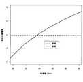
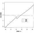
図8には、人工媒質100(誘電体層120の積層数:3層)において、厚さ方向に平行に伝播する入射電磁波の電界の方向を変化させた際に得られる、周波数と実効比透磁率の関係を示す。なお、電界方向0゜は、図3における電磁波150の電界Eの方向(すなわちY方向)に相当し、電界方向90゜は、図3におけるX方向を意味する。図8において、入射電磁波の電界の方向が0゜〜90゜の範囲で変化しても、周波数と実効比透磁率の関係はほとんど変化していないことがわかる。この結果から、入射電磁波の電界の方向が実効比透磁率に及ぼす影響は極めて小さく、人工媒質100では、実効比透磁率の偏波依存性が小さいと言える。 FIG. 8 shows the frequency and effective relative permeability obtained when the direction of the electric field of the incident electromagnetic wave propagating parallel to the thickness direction is changed in the artificial medium 100 (the number of laminated dielectric layers 120: 3 layers). The relationship of magnetic susceptibility is shown. The
なおこのような効果が得られる理由は、次のように考えられる。図9に示すように、入射する電磁波の電界Eのy軸となす角をαとし、電界Eをx成分(Ex)とy成分(Ey)に分解し、それぞれが導電性素子に作用する現象をベクトル合成する。電界Eのx成分Exは、電流Iのx成分Ixに比例し、このIxは、磁界Hのy成分Hyに比例する。電界、電流のy成分EyおよびIyと、磁界のx成分Hxについても同様である。この関係は、いかなるαにおいても成り立つ。一方、導電性素子のx方向の長さとy方向の長さは等しいため、これによる磁気共鳴周波数は等しく、磁界のxおよびy成分Hx、Hyの位相も等しくなる。従って、あらゆる角度αにおいて、合成された磁界Hの大きさは変化せず、その方向は、電界Eと直交することになる。これにより、入射電磁波の電界の方向が実効比透磁率に及ぼす影響は、極めて小さくなる。 The reason why such an effect can be obtained is considered as follows. As shown in FIG. 9, the angle formed by the y-axis of the electric field E of the incident electromagnetic wave is α, the electric field E is decomposed into an x component (Ex) and a y component (Ey), and each phenomenon acts on the conductive element. Is vector-combined. The x component Ex of the electric field E is proportional to the x component Ix of the current I, and this Ix is proportional to the y component Hy of the magnetic field H. The same applies to the y component Ey and Iy of the electric field and current and the x component Hx of the magnetic field. This relationship holds for any α. On the other hand, since the length in the x direction and the length in the y direction of the conductive element are equal, the magnetic resonance frequency by this is equal, and the phases of the x and y components Hx and Hy of the magnetic field are also equal. Therefore, the magnitude of the combined magnetic field H does not change at any angle α, and the direction thereof is orthogonal to the electric field E. Thereby, the influence of the direction of the electric field of the incident electromagnetic wave on the effective relative permeability is extremely small.
また、このような人工媒質100では、導電性素子130の縦横の幅、X方向およびY方向の配置ピッチ、導電性素子130同士間のギャップ等を独立に、自由に組み合わせることができるため、様々な機能を容易に発現させることが可能となる。 Further, in such an
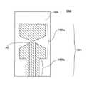
(第2の態様)
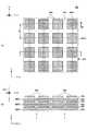
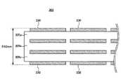
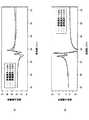
次に、図10を用いて、本発明による別の人工媒質の構成例について説明する。図10は、本発明による別の人工媒質800を示した図である。図10(a)は、人工媒質800の上面図、図10(b)は、B−B線での断面図である。(Second aspect)
Next, a configuration example of another artificial medium according to the present invention will be described with reference to FIG. FIG. 10 is a diagram illustrating another
人工媒質800は、前述の人工媒質100と同様に、導電面840を有する誘電体層820を複数枚積層させることにより構成される。また導電面840には、前述のような複数の導電性素子830が配列形成されている。ただし、人工媒質800は、さらに各誘電体層820の内部に、複数の直線状導体素子860を有する点が、前述の人工媒質100とは異なっている。なお、直線状導体素子860は、導電性素子830と同一の材料で構成されても良い。 The
各直線状導体素子860は、線幅d1(X方向の長さ)がほぼ等しく、誘電体層840の一端から他端に沿って(図10では、Y方向に沿って)、直線的に、相互に平行に延伸している。各直線状導体素子860は、図10(b)に示すように、それぞれ、実質的に各誘電体層820の厚みの中心部分に設置され、そのX方向の位置は、導電性素子830の領域と実質的に重なるように配置されている(特に、図10の例では、各直線状導体素子860は、導電性素子830の中央部近傍で重なるように配置されている)。また、各直線状導体素子860の線幅d1は、導電性素子830の幅(X方向の幅)よりも小さくなっている。ここで、図10の例では、各直線状導体素子860は、一定の距離間隔(ピッチ)で配置されており、さらにそのピッチは、導電性素子830のX方向の配置ピッチPとほぼ一致している。ただし、本発明は、このような構成に限られるものではない。例えば、各直線状導体素子860は、ランダムな距離間隔で配置されても良い。あるいは各直線状導体素子860のピッチは、導電性素子830の同方向の配置ピッチPと異なっていても良い。 Each
このような人工媒質800においても、入射電磁波150を受信する受信面と導電面840は一致しており、前述の効果を得ることができる。(ただしこの場合、良好な特性を得るため、直線状導体素子860の延伸方向(Y方向)が入射電磁波の電界Eの方向と平行となるようにして、直線状導体素子860を配置する必要があることに留意する必要がある。)また、このような人工媒質800では、導電性素子830および直線状導体素子860の形状、配置等を独立に、自由に組み合わせることができるため、様々な機能を発現させることが可能となる。例えば、人工媒質800は、後述のように、誘電率と透磁率が同時に負となる周波数領域を有する左手系媒質として使用することができる。 Even in such an
なお、図10の例では、直線状導体素子860は、Y方向に沿って延伸するように配置されているが、本発明は、このような態様に限られるものではない。すなわち、直線状導体素子860は、導電面と垂直な方向から見た際に、少なくとも一部に導電性素子と重なる領域を有する限り、いかなる方向に延伸しても良い。 In the example of FIG. 10, the
図11〜図14には、直線状導体素子を有する別の人工媒質が示されている。 FIGS. 11 to 14 show another artificial medium having a linear conductor element.
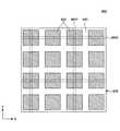
図11(a)、図11(b)(図11(a)のC−C断面図)に示す人工媒質801は、図10に示した人工媒質800とほぼ同様に構成されるが、この場合、各誘電体層820の内部には、Y方向に沿って誘電体層820の一端から他端まで延伸する複数の直線状導体素子860Y(図10の直線状導体素子860に相当する)のみならず、X方向に沿って誘電体層820の一端から他端まで延伸する複数の直線状導体素子860Xが形成されている点が異なっている。なお、直線状導体素子860Xは、導電性素子830と同一の材料で構成されても良い。各直線状導体素子860Xは、幅d2(Y方向の長さ)がほぼ等しく、直線的に、相互に平行に延伸している。また、各直線状導体素子860Xは、それぞれ、実質的に各誘電体層820の厚みの中心部分に設置され、そのY方向の位置は、導電性素子830の領域と実質的に重なるように配置されている(図11の例では、各直線状導体素子860Xは、導電性素子830の中央部近傍と重なるように配置されている)。また、図11の例では、直線状導体素子860XのY方向のピッチは、一定であり、このピッチは、導電性素子830の同方向の配置ピッチPとほぼ一致している。ただし、各直線状導体素子860Xは、ランダムな距離間隔で配置されても良い。また各直線状導体素子860Xのピッチは、導電性素子830の同方向の配置ピッチPと異なっていても良い。 The
このように構成された人工媒質801では、入射電磁波の磁界方向は、直線状導体素子860Xの延伸方向と平行であっても、直線状導体素子860Yの延伸方向と平行であっても良い。従って、前述の人工媒質800に比べて、電磁波150の電界および磁界の方向に対する配置の依存性が小さくなり、より適用の自由度が広がる。 In the
図12に示す人工媒質802は、図11に示した人工媒質801とほぼ同様に構成されるが、この場合、直線状導体素子860Xおよび860Yのピッチは、それぞれ、人工媒質801のY方向およびX方向の配置ピッチに比べて2倍に広がっている。 The
また、図13に示す人工媒質803は、図11に示した人工媒質801とほぼ同様に構成されるが、この場合、2種類の直線状導体素子(直線状導体素子860V、860W)は、それぞれ、図のX方向およびY方向から45゜だけ回転した方向に延伸している。 Further, the
また、図14に示す人工媒質803Aは、図13に示した人工媒質803とほぼ同様に構成される。ただしこの場合、導電性素子830は、人工媒質の厚さ方向から見たとき、直線状導体素子860V、860Wの全ての交点に配置されている。 Further, the
さらに図には示さないが、導電性素子と直線状導体素子は、この他にも、相互に様々な配置を取り得ることは、当業者には明らかであろう。 Further, although not shown in the drawings, it will be apparent to those skilled in the art that the conductive element and the linear conductor element can take other various arrangements.
ところで、前述のような2方向に延伸する直線状導体素子860X(以下、「第1の直線状導体素子」という)および860Y(以下、「第2の直線状導体素子」という)を有する人工媒質において、人工媒質の厚さ方向に平行な方向から見たとき、導電性素子830は、直線状導体素子860Xと直線状導体素子860Yとの各交点に配置されること(すなわち図11の人工媒質801の構成)が好ましい。以下、その理由を説明する。 By the way, the artificial medium having the
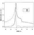
例えば、図15に模式的に示すように、第1の直線状導体素子860XのピッチをPYとし、第2の直線状導体素子860YのピッチPXをとしたとき、導電性素子830のX方向の配置ピッチPAおよびY方向の配置ピッチPBが、それぞれ、PA=2PX、PB=2PYとなっている場合を考える。ここで、各導電性素子830は、人工媒質の厚さ方向に平行な方向から見たとき、第1の直線状導体素子860Xと第2の直線状導体素子860Yの交点に配置されている。ただし、この人工媒質801Wでは、人工媒質の厚さ方向に平行な方向から見たとき、各導電性素子830の周囲に、導電性素子が配置されていない直線状導体素子の交点(8箇所)が存在する。すなわち、この人工媒質801Wでは、人工媒質の厚さ方向に平行な方向から見たとき、各導電性素子830は、その周囲が第1および第2の直線状導体素子によって完全に覆われており、導電面840に、いわば「枠で囲まれた導電性素子」として配置されているとも見なすことができる。なお、人工媒質801Wのその他の構成は、前述の人工媒質801と同様である。For example, as schematically shown in FIG. 15, when the pitch of the first
このように構成された人工媒質801Wのシミュレーション結果を図16に示す。また、前述の人工媒質801の同様のシミュレーション結果を図17に示す。シミュレーションには、FIT(FInite Integration Technique)法(有限積分法)を用いた。また、シミュレーションに使用した人工媒質801Wおよび801の各パラメータ値を表1に示す。なお両人工媒質において、誘電体層820の積層数は、1層とした。また各誘電体層820の厚さは、0.2mmとし、誘電体層111の誘電率は、4.0とし、誘電損は、0.001とした。また、各導電性素子830の寸法は、3mm×3mmとし、厚さは、10μmとした。第1および第2の直線状導体素子860Xおよび860Yの幅(d2)は、いずれも2.5mmとし、厚さはいずれも0.2mmとした。 FIG. 16 shows the simulation result of the artificial medium 801W configured as described above. Further, FIG. 17 shows a similar simulation result of the

なお、図16に示すような比実効誘電率の大きなピークは、いわゆる「枠で囲まれた導電性素子」を有する人工媒質801Wにおいて、各パラメータ値(例えば、直線状導体素子の幅d2、ピッチPX、PA等)を変化させた場合においても同様に認められた。It should be noted that the large peak of the relative effective dielectric constant as shown in FIG. 16 indicates that each parameter value (for example, the width d2 and the pitch of the linear conductor element) in the artificial medium 801W having a so-called “framed conductive element”. PX, was observed also in the case of changing the Pa, etc.).
以上のことから、導電性素子は、人工媒質の厚さ方向に平行な方向から見たとき、第1の直線状導体素子860Xと第2の直線状導体素子860Yとの各交点に配置されることがより好ましいと言える。 From the above, the conductive element is disposed at each intersection of the first
(第3の態様)
以上、導電性素子が2次元周期配列的に配置された導電面を、厚さ方向に2面以上積層することにより構成された人工媒質を例に、本発明を説明した。しかしながら、本発明の人工媒質は、このような構成に限られるものではない。すなわち、各導電面に単一の導電性素子が配置された人工媒質においても、前述の効果を得ることができる。(Third aspect)
The present invention has been described above by taking as an example an artificial medium configured by laminating two or more conductive surfaces in which the conductive elements are arranged in a two-dimensional periodic array in the thickness direction. However, the artificial medium of the present invention is not limited to such a configuration. That is, the above-described effect can be obtained even in an artificial medium in which a single conductive element is disposed on each conductive surface.
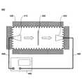
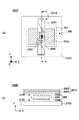
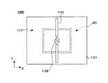
以下、図18〜図20を用いて、そのような構成を有する本発明のさらに別の人工媒質(第3の態様)の一例について詳しく説明する。ここで図18(a)は、本発明の第3の態様の人工媒質900の上面図であり、図18(b)は、人工媒質900のG−G断面図である。また、図19および図20は、それぞれ、そのような人工媒質900を備える第1のアンテナ装置の分解構成図および断面図を概略的に示したものである。 Hereinafter, an example of still another artificial medium (third aspect) of the present invention having such a configuration will be described in detail with reference to FIGS. Here, FIG. 18A is a top view of the
本発明の第3の態様の人工媒質900は、図18(a)、(b)に示すように、誘電体層920の表裏面のそれぞれに、同一の寸法形状の単一の導電性素子930a、930bを有する。従って、誘電体層920の表裏面が導電面940(940a、940b)に相当する。また、導電性素子930a、930bは、人工媒質の厚さ方向(Z方向)に沿って、位置が揃っている。なお図において、導電性素子930a、930bは、正方形状である。しかしながら、導電性素子の形状は、両方の形状(および寸法)が同一で限り、正方形に限られず、例えば、矩形状、三角形状、多角形状、円状、楕円状であっても良い。 As shown in FIGS. 18A and 18B, the
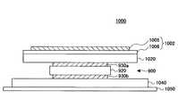
本発明による人工媒質900では、導電性素子930a、930bの大きさを調整することにより、インピーダンスマッチングが可能な周波数を調整することができる。従って、このような構成の人工媒質900は、例えば、図19、図20に示すような第1のアンテナ装置1000に適用することができる。 In the
第1のアンテナ装置1000は、アンテナ素子1002、第1のスペーサ層1020、前述の人工媒質900、第2のスペーサ層1040、および金属板1050をこの順に積層することにより構成される。アンテナ素子1002は、図19の破線で示すように、後述する放射素子1005の中心部ACが、人工媒質900の中心と重なるようにして、人工媒質900の上部に設置される。 The
アンテナ素子1002は、アンテナ基板1006と、この表面に印刷等の方法により設置された導体1005とを有する。アンテナ基板1006は、可撓性であることが好ましい。第1のスペーサ層1020は、誘電体または絶縁体で構成され、アンテナ素子1002の導体1005と人工媒質900の導電性素子930(930a)とが電気的に接触することを防止するために、アンテナ素子1002と人工媒質900の間に配置される。従って、アンテナ素子1002のアンテナ基板1006が誘電体または絶縁体で構成される場合、第1のスペーサ層1020は、省略しても良い。同様に第2のスペーサ層1040は、誘電体または絶縁体で構成され、人工媒質900の導電性素子930(930b)と金属板1050とが電気的に接触することを防止するために、両者の間に配置される。導体1005、導電性素子930a、bおよび金属板は、いかなる導電性材料で構成されても良く、例えば、銅またはアルミニウム等の金属で構成される。 The
図21には、アンテナ素子1002の導体1005の一形状を示す。この図の例では、導体1005は、放射素子1005aと給電線路1005bとで構成されている。ただし、本アンテナ装置において、導体1005の形状は、これに限られるものではないことは当然である。 FIG. 21 shows one shape of the
一般に、アンテナ装置は、他の金属が近接した状態では、特性が劣化することが知られている。従って、金属板を近傍に備えるアンテナ装置を適正に作動させるためには、比較的厚い誘電体または絶縁体の層(例えば、前述の第1および第2のスペーサ層)を金属板とアンテナ素子の間に介在させる必要がある。しかしながらこのような厚い介在層の設置は、アンテナ装置の小型化、低背化の障害となる。 In general, it is known that the characteristics of an antenna device deteriorate when other metals are close to each other. Therefore, in order to properly operate the antenna device including the metal plate in the vicinity, a relatively thick dielectric or insulator layer (for example, the first and second spacer layers described above) is formed between the metal plate and the antenna element. It is necessary to intervene. However, installation of such a thick intervening layer is an obstacle to miniaturization and low profile of the antenna device.
これに対して、前述のような本発明による人工媒質900を備える第1のアンテナ装置1000では、後述のように、金属板がアンテナ素子の近傍に配置されても、適正に作動することが確認されている。これは、アンテナ素子と金属板の間に、本発明による人工媒質を介在させることにより、人工媒質と金属板とが同相反射板として機能するためである。 On the other hand, it is confirmed that the
従って、本発明による人工媒質900を備える第1のアンテナ装置1000では、厚い介在層を設ける必要はなく、装置全体の小型化、低背化が可能となるという効果が得られる。 Therefore, in the
なお、本アンテナ装置は、広帯域アンテナ装置に限られるものではなく、電波を空間に放射する機能を有するものであれば、いかなるアンテナ装置であっても良いことに留意する必要がある。例えば、ダイポールアンテナ、ループアンテナ、メアンダラインを用いた線状アンテナ、スロットアンテナなどから選ぶことができる。また、アンテナ装置1000および/または人工媒質900が動作する動作周波数は個別に設定することができるので、前述の構成のアンテナ装置は、例えば、地上デジタル放送、携帯電話、RFID、VICS、ETC、無線LAN、などに用いることができる。 It should be noted that the present antenna device is not limited to the broadband antenna device, and may be any antenna device as long as it has a function of radiating radio waves into space. For example, it can be selected from a dipole antenna, a loop antenna, a linear antenna using a meander line, a slot antenna, and the like. In addition, since the operating frequency at which the
次に、前述のような、各導電面に単一の導電性素子が配置された人工媒質900の別の適用例について説明する。 Next, another application example of the
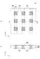
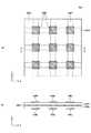
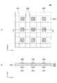
図22および図23には、それぞれ、前述の人工媒質900を3つ使用して構成される第2のアンテナ装置の上面図およびこのアンテナ装置のH−H線での断面図を示す。第2のアンテナ装置1100は、アンテナ素子群1120(図23参照)と、誘電体基板1150と、人工媒質群901(図23参照)と、をこの順に積層することにより構成される。 FIG. 22 and FIG. 23 show a top view of a second antenna device configured using three of the above-described
誘電体基板1150の上面には、アンテナ素子群1120が配置され、誘電体基板1150の下面には、人工媒質群901が配置される。 An
アンテナ素子群1120は、3つのアンテナ素子1120A〜1120Cを有する。各アンテナ素子1120A〜1120Cは、平面ダイポールアンテナ素子として構成され、給電点1125A〜Cと、導体1130A〜1130Cとを有する。これらの導体1130A〜1130Cは、誘電体基板1150の上面(XY平面)上に、Y軸に対して反時計回りに45゜回転した状態で配置される。 The
人工媒質群901は、第1〜第3の人工媒質900A、900Bおよび900Cを有する。各人工媒質は、誘電体基板1150の下面に導電面が形成されるように、X方向に沿って一列に配置することにより構成される。なお、これらの人工媒質900A〜900Cは、いずれも前述の人工媒質900と同様のものであり、一つの誘電体層(920A〜920C)の表裏面に、同一の矩形状の導電性素子(931A〜931C)を一つだけ配置して構成される。 The
ここで、第1の人工媒質900Aおよび第3の人工媒質900Cは、導電性素子931A、931Cの長手方向が図のY方向と平行になるように配置されているのに対して、第2の人工媒質900Bは、導電性素子931Bの長手方向が図のX方向と平行になるように配置されていることに留意する必要がある。 Here, the first
なお前述の各給電点1125A〜1125Cは、上部(Z方向)から見た場合、人工媒質群901のそれぞれの人工媒質の導電性素子931A〜931Cの中心に位置するように設けられている。 The feeding points 1125A to 1125C described above are provided so as to be positioned at the centers of the conductive elements 931A to 931C of the artificial media in the
このように構成されたアンテナ装置1100(以下、「本発明による第2のアンテナ装置」という)は、人工媒質群901を有さない同様のアンテナ装置(以下、「通常のアンテナ装置」と称する)に比べて以下の特徴を有する。 An
通常のアンテナ装置の場合、各アンテナ素子1120A〜1120Cから得られる電磁波の磁界は、導体1130に沿った方向、すなわち、図22のY方向から反時計回りに45゜傾斜した角度となる。これは、いずれのアンテナ素子においても等しい。この場合、給電点1125の間隔SPが接近しすぎると、隣接するアンテナ素子の電磁波がカップリングしてしまうため、間隔SPは、あまり近づけることはできない。従って、通常のアンテナ装置では、小型化することは難しい。 In the case of a normal antenna device, the magnetic field of the electromagnetic wave obtained from each of the
これに対して、本発明による第2のアンテナ装置1100では、各アンテナ素子から得られる電磁波の磁界方向は、人工媒質群901の影響を受ける。特に、中央のアンテナ素子1120Bでは、第2の人工媒質900Bは、隣接する両人工媒質900A、900Cに対して導電性素子の方向が90゜ずれているため、このアンテナ素子1120Bにより得られる電磁波の磁界方向は、両側のアンテナ素子1120A、1120Cの電磁波の磁界方向に対して、直交する。このため、本発明による第2のアンテナ装置1100では、給電点の間隔を接近させることができ、すなわち隣接するアンテナ素子同士の間隔を狭めることができる。 On the other hand, in the
従って、本発明による第2のアンテナ装置では、従来のアンテナ装置に比べて、より小型化、集積化することが可能となる。 Therefore, the second antenna device according to the present invention can be made smaller and more integrated than the conventional antenna device.
なお、上記第3の態様では、それぞれが単一の素子を有する2つの導電面からなる人工媒質を例に、本発明の構成を説明した。しかしながら、このような第3の人工媒質において、人工媒質が厚さ方向に沿って導電面を3層以上有しても良いことは、当業者には明らかであろう。 In the third aspect, the configuration of the present invention has been described by taking as an example an artificial medium composed of two conductive surfaces each having a single element. However, it will be apparent to those skilled in the art that in such a third artificial medium, the artificial medium may have three or more conductive surfaces along the thickness direction.
次に、図24および図25を用いて、本発明のさらに別のアンテナ装置(第3のアンテナ装置)の一例について詳しく説明する。ここで図24は、本発明の第3のアンテナ装置1300の概略的な上面図であり、図25は、第3のアンテナ装置1300の概略的なJ−J断面図である。なおアンテナ装置1300を構成する各素子において、前述のアンテナ装置1100と同様の素子には、同一の参照符号が付されている。 Next, an example of still another antenna device (third antenna device) of the present invention will be described in detail with reference to FIG. 24 and FIG. Here, FIG. 24 is a schematic top view of the
第3のアンテナ装置1300は、前述の第2のアンテナ装置1100と同様、前述の人工媒質900を使用して構成される。ただし、このアンテナ装置1300では、人工媒質900が一つだけ使用される。すなわち、第3のアンテナ装置1300は、アンテナ素子1120と、誘電体基板1150と、人工媒質900とをこの順に積層することにより構成される。 Similar to the
アンテナ素子1120は、平面ダイポールアンテナ素子として構成され、給電点1125と、導体1130とを有する。導体1130は、誘電体基板1150の上面(XY平面)上に、Y軸に対して反時計回りに45゜回転した状態で配置される。 The
人工媒質900は、前述の第2のアンテナ装置1100に使用される人工媒質900と同様のものであり、一つの誘電体層920の表裏面に、同一の矩形状の導電性素子931を一つずつ配置して構成される。 The
ここで、前述の給電点1125は、上部(Z方向)から見た場合、人工媒質900の導電性素子931の中心に位置するように設けられている。 Here, the above-described
このように構成された第3のアンテナ装置1300は、後述のように、人工媒質900を有さない同様のアンテナ装置に比べて、多共振であり、広帯域で作動するという特徴を有する。 As will be described later, the
以下、本発明の実施例について説明する。 Examples of the present invention will be described below.
(実施例1)
以下の手順で本発明の人工媒質を試作し、得られた人工媒質の特性を評価した。Example 1
The artificial medium of the present invention was prototyped according to the following procedure, and the characteristics of the obtained artificial medium were evaluated.
まず、一般的なプリント配線基板材料であるFR4(Flame Retardant Grade−4)と、一般的な多層プリント配線基板プロセスを用いて、一辺が150mmの人工媒質の試作を行った。厚みが0.2mm のコア層の両面に導電性素子を配置し、導体には厚み18μmの銅箔を用いた。導電性素子は、1辺Q=3mmの正方形状であり、面内での導電性素子同士の間隔Gは、1mmである。人工媒質の四辺の端部から最近接の導電性素子までの距離GSは、1.5mmとし、縦横それぞれ37個の導電性素子を設置した。 First, an artificial medium having a side of 150 mm was prototyped using a general printed wiring board material FR4 (Frame Regentant Grade-4) and a general multilayer printed wiring board process. Conductive elements were disposed on both sides of a core layer having a thickness of 0.2 mm, and a copper foil having a thickness of 18 μm was used as the conductor. The conductive elements have a square shape with one side Q = 3 mm, and the distance G between the conductive elements in the plane is 1 mm. The distance GS from the ends of the four sides of the artificial medium to the nearest conductive element was 1.5 mm, and 37 conductive elements were installed in each of the vertical and horizontal directions.
次に、このように表裏面に導電性素子の配列パターンを形成した2つのコア層を、導電性素子を設置していない、同寸法(すなわち、長さ150mm×幅150mm×厚さ0.2mm)のプリプレグ層を介在させた状態で積層した。さらに、この積層体に積層方向から均一な押圧(2〜3MPa程度)を加えた状態で、積層体を170℃以上の温度に昇温してプリプレグ層を溶融させることにより、3枚の層を接着させ、人工媒質を製作した。積層体の昇温速度は、1.5〜3.5℃/分程度とし、積層体は、170℃以上の温度で少なくとも20分間保持した。なお、積層体の熱処理は、真空度4.0kPa以下の真空雰囲気で実施した。 Next, the two core layers in which the conductive element array pattern is formed on the front and back surfaces in this way have the same dimensions (that is,
得られた人工媒質300は、図26の断面図に模式的に示すように、3層の誘電体層部分320a〜cを含み、これらの誘電体層部分の間および人工媒質300の両最表面には、導電性素子330のパターンが配置された、合わせて4層の導電面を有する構造であった。また、この人工媒質300の最終的な厚さTは、0.63mmであった。これを実施例1に係る人工媒質と称する。 The obtained
次に、このようにして製作した実施例1に係る人工媒質を用いて、基板の積層方向と平行な方向に進行する電磁波を入射した際に、人工媒質に生じる実効比誘電率および実効比透磁率を測定した。 Next, the effective relative permittivity and effective relative permeability generated in the artificial medium when the electromagnetic wave traveling in the direction parallel to the substrate stacking direction is incident using the artificial medium according to the first embodiment manufactured in this way. The magnetic susceptibility was measured.
図27には、人工媒質の実効比誘電率および実効比透磁率測定用の測定装置の概略構成図を示す。この測定装置400は、送信用ホーンアンテナ410と、受信用ホーンアンテナ420と、電波吸収体430と、ベクトルネットワークアナライザー440とを有する。送信用ホーンアンテナ410と、受信用ホーンアンテナ420との間には、測定対象である前述のように製作された人工媒質300が設置される。送信用ホーンアンテナ410〜受信用ホーンアンテナ420までの測定領域全体は、電波吸収体430によって被覆されている。またベクトルネットワークアナライザー440は、同軸ケーブル460を介して、送信用ホーンアンテナ410および受信用ホーンアンテナ420に接続されている。本測定では、送信用ホーンアンテナ410および受信用ホーンアンテナ420には、コニカルホーンアンテナを使用した。送信用ホーンアンテナ410から受信用ホーンアンテナ420までの距離は、320.6mmであり、これらのアンテナ410、420から人工媒質300の表面までの距離は、160mmとした。 FIG. 27 shows a schematic configuration diagram of a measuring device for measuring the effective relative permittivity and effective relative permeability of an artificial medium. The measuring
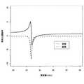
このような測定装置400を用いて、次のようにして実施例1に係る人工媒質の実効比誘電率および実効比透磁率を求めた。まず、ベクトルネットワークアナライザー440を用いて、自由空間法により人工媒質300のSパラメータを計測する。次に、得られた結果から、以下の文献(1)〜(3)に記載されている計算アルゴリズムを用いて、実施例1に係る人工媒質300の実効比誘電率および実効比透磁率を算出した:
(1)A.M.Nicolson,G.F.Ross,"Measurement of the Intrinsic Properties of Materials by Time Domain Techniques",IEEE Transaction on IM. No.4,Nov.,1970年
(2)W.B.Weir,"Automatic Measurement of Complex Dielectric Constant and Permeability at Microwave Frequencies", Proc. of IEEE,Vol.62,Jan.,1974年
(3)J.B.Jarvis,E.J.Vanzura,"Improved Technique for Determining Complex Permittivity with the Transmission/Reflection Method", IEEE Transaction MTT,vol.38,Aug.,1990年。Using such a
(1) A. M.M. Nicolson, G.M. F. Ross, “Measurement of the Intrinsic Properties of Materials by Time Domain Techniques”, IEEE Transaction on IM. No. 4, Nov. (2) W., 1970. B. Weir, “Automatic Measurement of Complex Direct Constant and Permeability at Microwave Frequencies”, Proc. of IEEE, Vol. 62, Jan. 1974 (3) J. Am. B. Jarvis, E .; J. et al. Vanzura, “Improved Technology for Determining Complex Permitency with the Transmission / Reflexion Method”, IEEE Transaction MTT, vol. 38, Aug. 1990.
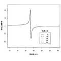
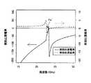
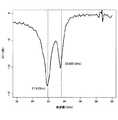
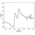
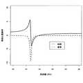
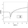
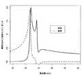
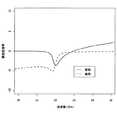
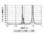
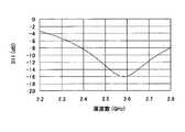
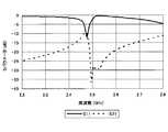
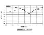
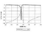
図28には、前述の装置400を用いた測定によって得られた、実施例1に係る人工媒質のSパラメータ(S11)の振幅特性を示す。また、図29には、実施例1に係る人工媒質のSパラメータ(S11)の位相特性の測定結果を示す。さらに図30には、これらの結果を用いて、前述の計算アルゴリズムによって算出した、実施例1に係る人工媒質の実効比誘電率(上段)と実効比透磁率(下段)の周波数特性を示す。図30から、実施例1に係る人工媒質の実効比透磁率は、周波数とともに増加し、21.9GHzにおいて極大値 (6.07)が得られ、23.625GHzの周波数において、最大値(11.16)が得られることがわかる。また、図28のSパラメータの振幅特性の結果から、実効比透磁率がピークを示す21.9GHzと23.625GHzの周波数において、人工媒質が整合していることがわかる。 FIG. 28 shows the amplitude characteristic of the S parameter (S11) of the artificial medium according to Example 1 obtained by measurement using the above-described
(実施例2)
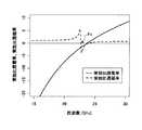
次に、2層の誘電体層と、導電性素子のパターンが設置された3層(誘電体層の間および人工媒質の表裏の最表面)の導電面とで構成される人工媒質(以下、「実施例2に係る人工媒質」という)を想定し、得られる特性をシミュレーションで予測した。(Example 2)
Next, an artificial medium composed of two dielectric layers and three layers (the outermost surfaces between the dielectric layers and the front and back surfaces of the artificial medium) on which conductive element patterns are installed (hereinafter referred to as the artificial medium) Assuming “artificial medium according to Example 2”), the obtained characteristics were predicted by simulation.
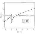
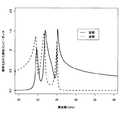
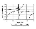
図31には、実施例2に係る人工媒質において得られた、実効比誘電率および実効比透磁率のシミュレーション結果を示す。なお、この計算には、FIT(Finite Integration Technique)法(有限積分法)による3次元電磁界シミュレーションを用いた。また層間の誘電体層は、誘電率を4.2とし、誘電損失を0.005、0.015および0.025の3種類として計算を行った。図31から、誘電損失が0.005の場合、誘電損失が0.025の場合に比べて、周波数約22.8GHzにおける実効比透磁率のピーク値が大きくなっていることがわかる。 FIG. 31 shows simulation results of effective relative permittivity and effective relative permeability obtained in the artificial medium according to Example 2. For this calculation, a three-dimensional electromagnetic field simulation by a FIT (Finite Integration Technique) method (finite integration method) was used. In addition, the dielectric layers between the layers were calculated with a dielectric constant of 4.2 and a dielectric loss of 0.005, 0.015, and 0.025. FIG. 31 shows that the peak value of the effective relative permeability at a frequency of about 22.8 GHz is larger when the dielectric loss is 0.005 than when the dielectric loss is 0.025.
この結果から、誘電損失の少ない材料を誘電体層として使用することにより、実効比透磁率のピーク値を大きくすることができる。例えば、ロジャース(ROGERS)社のRT/Duroid5880(誘電率2.2、誘電損失0.0009)、またはROGERS社のRO3003(誘電率3.0、誘電損失0.0013)等のフッ素樹脂系の材料を使用することにより、実効比透磁率のピーク値を大きくすることができると考えられる。 From this result, the peak value of the effective relative permeability can be increased by using a material having a small dielectric loss as the dielectric layer. For example, RT / Duroid 5880 (dielectric constant 2.2, dielectric loss 0.0009) of ROGERS, or RO3003 (dielectric constant 3.0, dielectric loss 0.0013) of ROGERS It is considered that the peak value of the effective relative permeability can be increased by using.
(実施例3)
次に、図32に示すような導電性素子および直線状導体素子の配置を有する人工媒質(以下、「実施例3に係る人工媒質804」という)を想定し、この特性を実施例2と同様のシミュレーションを用いて予測した。なお図32(b)は、図32(a)のD−D線に沿った断面図である。ここで、実施例3に係る人工媒質804は、次のような構成であると仮定した。すなわち、人工媒質804は、第1の誘電体層820aと第2の誘電体層820bとの間に設置された直線状導体素子860のパターン、第1の誘電体層820aの下側に配置された導電性素子830aのパターン、ならびに第2の誘電体層820bの上面に配置された導電性素子830aのパターンで構成されると仮定した。また実施例3に係る人工媒質の各パラメータは、表2のように設定した。なお、誘電体層の比誘電率は、4.0であり、誘電損失は、0.01である。また、導電性素子および直線状導体素子の導電率は、6.29×10⁷S/mである。(Example 3)
Next, an artificial medium having an arrangement of conductive elements and linear conductor elements as shown in FIG. 32 (hereinafter referred to as “
図33〜図36には、シミュレーションの結果を示す。なお、この媒質に入射される電磁波は、磁界方向が図32のX方向と平行であり、電界方向がY方向と平行なものである。図33には、実施例3に係る人工媒質804の実効比誘電率の周波数依存性を示す。この図から、周波数22GHz〜24GHz近傍で、実効比誘電率の実部が負となる領域が出現していることがわかる。また、図34には、実施例3に係る人工媒質804の実効比透磁率の周波数依存性を示す。この図から、同等の領域(周波数22〜24GHz近傍)に、実効比透磁率の実部が負となる領域が出現していることがわかる。さらに、図35には、実効屈折率の周波数依存特性を示すが、この図から、周波数22〜24GHz近傍において屈折率が負となっており、いわゆる左手系媒質が得られていることがわかる。また、図36には、規格化された実効インピーダンス(すなわち、自由空間のインピーダンスに対する媒質のインピーダンスの比)の周波数依存性を示すが、前述の周波数領域において、規格化されたインピーダンスは、ほぼ1前後の値を示している。この結果は、本発明による人工媒質が、左手系媒質として良好な特性を発揮し得ることを示している。 33 to 36 show simulation results. The electromagnetic wave incident on this medium has a magnetic field direction parallel to the X direction in FIG. 32 and an electric field direction parallel to the Y direction. FIG. 33 shows the frequency dependence of the effective relative permittivity of the
(実施例4)
次に、図37に示すような導電性素子および直線状導体素子の配置を有する人工媒質(以下、「実施例4に係る人工媒質805」という)を想定し、この特性を実施例2と同様のシミュレーションを用いて予測した。なお図37(b)は、図37(a)のE−E線に沿った断面図である。実施例4に係る人工媒質805は、前述の実施例3の人工媒質804と同様の構成であると仮定した。ただし、この実施例では、第1の誘電体層820aと第2の誘電体層820bとの間に、直線状導体素子860Xおよび860Yが設置されている点が異なっている。直線状導体素子860Xは、図のX方向に延伸し、直線状導体素子860Yは、図のY方向に延伸している。実施例4に係る人工媒質の各パラメータは、表3のように設定した。なお、誘電体層の比誘電率は、4.0であり、誘電損失は、0.01である。また、導電性素子および直線状導体素子の導電率は、6.29×10⁷S/mである。Example 4
Next, an artificial medium having an arrangement of conductive elements and linear conductor elements as shown in FIG. 37 (hereinafter referred to as “
図38〜図41には、シミュレーションの結果を示す。図38には、実施例4に係る人工媒質805の実効比誘電率の周波数依存性を示す。この図から、周波数約24GHz以下の範囲に、実効比誘電率の実部が負となる領域が出現していることがわかる。また、図39には、実施例4に係る人工媒質805の実効比透磁率の周波数依存性を示す。この図から、周波数23GHz〜24GHzの範囲に、実効比透磁率の実部が負となる領域が出現していることがわかる。さらに、図40には、実効屈折率の周波数依存特性を示すが、この図から、周波数22GHz〜24GHzの範囲において屈折率が負となっており、いわゆる左手系媒質が得られていることがわかる。また、図41には、規格化された実効インピーダンス(すなわち、自由空間のインピーダンスに対する媒質のインピーダンスの比)の周波数依存性を示すが、22GHz〜24GHzの周波数領域において、規格化された実効インピーダンスは、ほぼ1に近い値を示している。この結果は、本発明による人工媒質が、左手系媒質として良好な特性を発揮し得ることを示している。 38 to 41 show simulation results. FIG. 38 shows the frequency dependence of the effective relative permittivity of the
(実施例5)
次に、図42に示すような導電性素子および直線状導体素子の配置を有する人工媒質(以下、「実施例5に係る人工媒質806」という)を想定し、この特性を実施例2と同様のシミュレーションを用いて予測した。なお図42(b)は、図42(a)のF−F線に沿った断面図である。実施例5に係る人工媒質805は、前述の実施例4の人工媒質805と同様の構成であると仮定した。ただし、この実施例では、導電性素子830a、830bの一辺の長さQは、直線状導体素子860X'、860Y'の幅d2、d1よりも小さくなっている点が実施例4とは異なっている。実施例5に係る人工媒質の各パラメータは、表4のように設定した。なお、誘電体層の比誘電率は、4.0であり、誘電損失は、0.01である。また、導電性素子および直線状導体素子の導電率は、6.29×10⁷S/mである。(Example 5)
Next, an artificial medium having an arrangement of conductive elements and linear conductor elements as shown in FIG. 42 (hereinafter referred to as “
本願において、図32、図37、図42等に示す構成の人工媒質(すなわち、直線状導体素子を有する人工媒質)については、具体的な製作例を示さなかったが、これらの人工媒質も、実施例1と同様の技術、すなわち、一般的なプリント配線基板材料であるFR4と、一般的な多層プリント配線基板プロセスを用いて、容易に製作することができることは当業者には明らかである。この場合、一つの誘電体層の上部に直線状導体素子のパターンを形成した後、その上部を別の誘電体層で被覆するステップが追加される。 In the present application, the artificial medium having the configuration shown in FIGS. 32, 37, 42, etc. (that is, an artificial medium having a linear conductor element) has not been shown as a specific manufacturing example. It will be apparent to those skilled in the art that it can be easily manufactured using the same technique as in Example 1, that is, FR4, which is a general printed wiring board material, and a general multilayer printed wiring board process. In this case, after the pattern of the linear conductor element is formed on the top of one dielectric layer, a step of covering the top with another dielectric layer is added.
(実施例6)
次に、前述の第3の態様による人工媒質を備えるアンテナ装置(図19〜図21に示すアンテナ装置)を試作し、その特性を評価した。アンテナ装置は、以下のように製作した。
(人工媒質の製作)
誘電体層920の表裏面の各々に、単一の導電性素子930(930a、930b)を印刷し、前記表裏面を導電面940とする人工媒質900(図18参照)を製作した。(Example 6)
Next, an antenna device (the antenna device shown in FIGS. 19 to 21) provided with the artificial medium according to the above-described third aspect was prototyped and its characteristics were evaluated. The antenna device was manufactured as follows.
(Production of artificial medium)
A single conductive element 930 (930a, 930b) was printed on each of the front and back surfaces of the
誘電体層930の寸法形状は、100mm×100mm(厚さ0.762mm)の正方形とした。また、導電性素子930a、930bの寸法形状は、90mm×90mmの正方形とし、これらは、厚み方向に相互に位置が揃うように、誘電体層の表裏面のほぼ中央に配置した。誘電体層920には、熱硬化性樹脂(比誘電率3.38)を使用し、導電性素子930a、930bには、銅を使用した。
(アンテナ装置の製作)
アンテナ素子1002は、ポリイミド製の可撓性基板1006(縦245mm×横110mm)上に、銅を導体1005として印刷することにより製作した。The dimensional shape of the dielectric layer 930 was a square of 100 mm × 100 mm (thickness 0.762 mm). The dimensions of the
(Production of antenna device)
The
次に、このアンテナ素子1002を第1のスペーサ層1020(縦275mm×横130mm、厚さ0.762mm)を介して、前述の人工媒質900の上に積層した。さらに人工媒質900の下に、第2のスペーサ層1040(縦220mm×横220mm、厚さ0.762mm)を介して、金属板1050(縦300mm×横300mm、厚さ3mm)を配置し、アンテナ装置(実施例6に係るアンテナ装置)を製作した。第1のスペーサ層1020、第2のスペーサ層1040には、比誘電率が3.38で、厚さが0.762mmの熱硬化性樹脂を使用した。 Next, this
なお、前述の導体1005は、図21に示すような、放射素子1005aと、給電線路1005bとを有する形状とした。この場合、放射素子1005aへの給電は、給電線路1005bのコプレナーウェーブガイドにより行われる。放射素子1005a(形状は、図21の放射素子1005a参照)の外形寸法は、縦142mm×横99mmとした。給電線路1005bのインピーダンスは、50Ωであった。 Note that the above-described
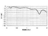
(特性評価)
前述のように製作したアンテナ装置の特性を評価した。アンテナ特性は、前述のベクトルネットワークアナライザーを用いて、リターンロス(S11特性)を測定することにより実施した。(Characteristic evaluation)
The characteristics of the antenna device manufactured as described above were evaluated. The antenna characteristic was implemented by measuring the return loss (S11 characteristic) using the vector network analyzer described above.
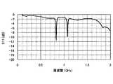
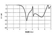
図47には、前述のアンテナ素子1002単独の場合に得られた、S11特性を示す。周波数500MHz付近から、S11値が−10dBを下回るようになり、広帯域アンテナとして適正に作動することがわかる。 FIG. 47 shows S11 characteristics obtained in the case of the
図48は、実施例6に係るアンテナ装置の同様の測定結果を示したものである。この結果から、実施例6に係るアンテナ装置では、約835MHzおよび約1070MHzの周波数において、インピーダンスがマッチングしていることがわかる。 FIG. 48 shows the same measurement result of the antenna device according to Example 6. From this result, it can be seen that in the antenna device according to Example 6, impedances are matched at frequencies of about 835 MHz and about 1070 MHz.
(比較例1)
次に、前述の実施例6と同様のアンテナ装置であって、アンテナ素子1002と金属板1050の間に人工媒質900を含まないアンテナ装置(比較例1)を試作し、同様の測定方法で、このアンテナ装置の特性を評価した。図49には、比較例1に係るアンテナ装置1000Bの概略断面図を示す。この図において、実施例6のアンテナ装置(すなわち図19〜図21)と同様の部材には、同一の参照符号が付されていることに留意する必要がある。(Comparative Example 1)
Next, an antenna device (Comparative Example 1) that is the same antenna device as that of the above-described Example 6 and does not include the
測定結果を図50に示す。この結果から、本発明による人工媒質900を有さないアンテナ装置では、インピーダンスがマッチングしていないことがわかる。 The measurement results are shown in FIG. From this result, it can be seen that the impedance is not matched in the antenna device without the
図48と図50の比較から、本発明による人工媒質900を備えるアンテナ装置では、金属と近接した状態でも、適正に作動することが示された。 Comparison between FIG. 48 and FIG. 50 indicates that the antenna device including the
通常、金属板をアンテナ装置の反射板として使用するためには、アンテナ素子と金属板の距離を、アンテナの動作周波数の波長の1/4だけ離す必要がある。従って、アンテナ装置の低背化は難しい。しかしながら、本発明による人工媒質900を用いることにより、両者間の距離を大幅に短縮することができる。すなわち、本発明による人工媒質900を備えるアンテナ装置では、アンテナ素子と金属板との間に、厚い誘電体または絶縁体の層を介在させる必要がなくなり、アンテナ装置の小型化、低背化を実現することが可能となる。 Usually, in order to use a metal plate as a reflector of an antenna device, the distance between the antenna element and the metal plate needs to be separated by ¼ of the wavelength of the antenna operating frequency. Therefore, it is difficult to reduce the height of the antenna device. However, by using the
(実施例7)
次に、前述の第3の態様による人工媒質を備える別のアンテナ装置2000について、その特性をシミュレーションにより評価した。(Example 7)
Next, the characteristics of another
別のアンテナ装置2000は、図51(a)(b)に示すような構成とした。図51(b)は、図51(a)のK−K断面の概略図である。(ただし、図51(b)において、実際にはパターン形成されている放射導体2020は、簡略化して示されていることに留意する必要がある。)
図51に示すように、別のアンテナ装置2000は、金属板2150、前述の人工媒質900、およびアンテナ素子2010をこの順に積層することにより構成される。アンテナ素子2010は、UHF帯RFIDタグ(Omron製:Waveインレット)であり、このアンテナ素子2010は、PET(Polyethylene Terephtha late)フィルム2040上に放射導体2020が印刷形成されたものである。なお、放射導体2020上には、ICチップ2050が実装されている。アンテナ素子2010と人工媒質900の間、および人工媒質900と金属板2150の間には、両者を電気的に絶縁するため、それぞれ空気層2160および2161が形成されている。Another
As shown in FIG. 51, another
フィルム2040の寸法は、100mm(Y方向の長さ)×20mm(X方向の長さ)×厚さ0.038mmとした。人工媒質900は、誘電率が3.38の誘電体層920(縦(Y方向の長さ)55mm×横(X方向の長さ)90mm×厚さ1mm)と、単一の導電性素子(930a、930b)(縦49.5mm×横81mm×厚さ0.01mm)とで構成される。フィルム2040は、図に示すように、フィルム2040の長手方向が矩形状の人工媒質900の長手方向と直交するようにして、人工媒質900の上部に設置した。金属板2150は、XY平面に無限に延在しており、その厚さは0.01mmと仮定した。また、空気層2160および2161の厚さは、それぞれ0.462mmおよび0.5mmとした。 The dimension of the
このような別のアンテナ装置2000について、アンテナ特性を評価した。アンテナ特性は、FIT(FInite Integration Technique)法(有限積分法)をベースとした電磁界シミュレータ(Microwave Studio)を用いて実施した。結果を図52〜図54に示す。なお、シミュレーションでは、ICチップ2050の実装位置に給電点を設けた。 With respect to such another
図52は、別のアンテナ装置2000のS11特性を示したものである。また図53および図54は、それぞれ、アンテナ装置2000の入力インピーダンスの実部および虚部を示したものである。なお、図53、図54には、図51に示す配置のRFIDタグ2010を、XY平面において、図の位置から45゜および90゜回転させて配置した場合の結果を同時に示している。 FIG. 52 shows the S11 characteristic of another
図52に示すように、アンテナ装置2000は、990MHz近傍でS11が−10dBを下回り、良好な特性を示すことがわかる。また図54に示すように、アンテナ装置の入力インピーダンスの虚部は、RFIDタグ2010の回転角度とともに変化することがわかる。これは、RFIDタグ2010と人工媒質900の配置関係によって、アンテナ装置の入力インピーダンス(特に虚部の値)が変化することを示している。すなわち両者の配置を制御することにより、アンテナ装置2000の入力インピーダンスを最適な値に調整することができる。 As shown in FIG. 52, it can be seen that the
一般に、RFIDタグに金属物を設置した状態で、RFIDタグを通信可能にする場合、人工媒質を利用した同相反射板を利用することが有効であると考えられる。しかしながら、そのような装置では、RFIDタグの入力インピーダンスがICチップとミスマッチングを起こし、これにより通信性能が低下する場合がある。これに対して、本発明によるアンテナ装置の場合、RFIDタグの配置を調整することにより、アンテナ装置のインピーダンスをRFIDタグの入力インピーダンスに近づけることができるため、本発明のアンテナ装置では、良好な通信特性を得ることができる。 In general, it is considered effective to use an in-phase reflection plate using an artificial medium when the RFID tag can communicate with a metal object placed on the RFID tag. However, in such a device, the input impedance of the RFID tag may cause mismatching with the IC chip, which may reduce communication performance. On the other hand, in the case of the antenna device according to the present invention, the impedance of the antenna device can be brought close to the input impedance of the RFID tag by adjusting the arrangement of the RFID tag. Characteristics can be obtained.
(実施例8)
次に、前述の第3の態様による人工媒質を備える第2のアンテナ装置(図22〜図23に示すアンテナ装置)の特性をシミュレーションにより評価した。第2のアンテナ装置は、以下の構成とした。(Example 8)
Next, the characteristics of the second antenna device (the antenna device shown in FIGS. 22 to 23) including the artificial medium according to the third aspect described above were evaluated by simulation. The second antenna device has the following configuration.
3つの人工媒質900A〜900Cは、図18に示したような構成とした。誘電体層920の寸法は、縦21.7mm×横17.3mm×厚さ1mmとした。導電性素子の寸法は、横19.5mm×縦15.6mmとした。なお、前述のように、3つの人工媒質900A〜900Cのうち、中央に配置される人工媒質900Bは、残りの人工媒質900A、900Cに比べて、導電性素子931Bの長手方向が90゜回転された状態となるように、誘電体基板1150上に配置した。 The three
誘電体基板1150の寸法は、横21.7mm×縦17.3×厚さ1mmとした。誘電体基板の比誘電率は、9とした。 The dimensions of the
3つのアンテナ素子1120A〜Cにおいて、各導体1130A〜Cの外形寸法(全長と線幅)は、36mm×2mmとし、厚さは0.01mmとした。各導体1130A〜Cは、いずれもY軸に対して反時計回りに45゜回転した状態で配置した。各アンテナ素子間の間隔SPは、30mmとした。 In the three
このように構成されたアンテナ装置を実施例8に係るアンテナ装置と称する。 The antenna device configured as described above is referred to as an antenna device according to an eighth embodiment.
(特性評価)
前述のように製作した実施例8に係るアンテナ装置の特性をシミュレーションにより評価した。(Characteristic evaluation)
The characteristics of the antenna device according to Example 8 manufactured as described above were evaluated by simulation.
まず初めに、アンテナ素子単体の特性を確認するため、図55に示す一つのアンテナ素子1120Dのリターンロス特性を評価した。なお、図55(a)は、アンテナ素子1120Dの上面図であり、図55(b)は、アンテナ素子1120Dの断面図である。このアンテナ素子1120Dは、誘電体基板1150Dの表面に、導体1130Dと給電点1125Dを備える。誘電体基板1150Dの寸法は、横100mm×縦50mmで、比誘電率は9とした。結果を図56に示す。得られたS11特性から、約2.6GHzでアンテナ素子が効率的に作動することがわかる。 First, in order to confirm the characteristics of a single antenna element, the return loss characteristics of one
次に、図22、図23に示す構成のアンテナ装置について、解析を行った。結果を図57に示す。なお、この結果は、中央のアンテナ素子1120Bにおいて得られたものである。なお、シミュレーション結果において、S21特性とS31特性は等しいため、図57には、S11とS21のみを表示した。 Next, the antenna apparatus having the configuration shown in FIGS. 22 and 23 was analyzed. The results are shown in FIG. This result was obtained for the
以下の式により、整合周波数での放射効率を算出したところ、放射効率ηは、74.8%となった。 When the radiation efficiency at the matching frequency was calculated by the following equation, the radiation efficiency η was 74.8%.
放射効率η=1−S112−S212−S312
一方、同様の構成を有するものの、人工媒質群901を有さないアンテナ装置により得られた結果を図58に示す。前述の図57の場合と同様、この結果は、中央のアンテナ素子において得られたものである。この結果から、整合周波数での放射効率ηを算出したところ、ηは67.9%であった。このことから、人工媒質を有さないアンテナ装置では、中央のアンテナ素子が両側のアンテナ素子の干渉を受け、放射効率が低下するのに対して、人工媒質を有するアンテナ装置では、そのような干渉が生じにくく、高い放射効率が得られることがわかった。Radiation efficiency η = 1−S112 −S212 −S312
On the other hand, FIG. 58 shows the result obtained by the antenna device having the same configuration but not having the
この結果は、本発明による人工媒質を使用することにより、アンテナ素子同士を接近させることが可能となることを示しており、これによりアンテナ装置の小型化、低背化を実現することが可能となる。 This result shows that the antenna elements can be brought close to each other by using the artificial medium according to the present invention, which makes it possible to realize a reduction in size and height of the antenna device. Become.
(実施例9)
次に、図59に示す構成を有するアンテナ装置1200の特性をシミュレーションにより評価した。ここで、アンテナ装置1200は、前述のアンテナ装置1100と同様の構成を有する。しかしながら、本アンテナ装置1200は、3つのアンテナ素子1121A〜Cの導体1131A〜Cが、Y方向に平行に延伸している点、および人工媒質901の導電性素子がいずれも正方形状である点が、前述のアンテナ装置1100とは異なっている。Example 9
Next, the characteristics of the
このアンテナ装置1200の特性を、前述の実施例8の場合と同様のシミュレーションにより解析した結果を図60に示す。また、図61には、アンテナ装置1200において、人工媒質901A〜901Cを除去した場合の特性シミュレーション結果を示す。ここで図60および図61は、いずれも中央のアンテナ素子に対して得られた結果である。 FIG. 60 shows the result of analyzing the characteristics of the
両者において、整合周波数での放射効率ηを比較したところ、アンテナ装置1200の場合は、η=71.4%となり、人工媒質を有さないアンテナ装置では、η=65.4%となった。このことから、アンテナ装置1200では、人工媒質の設置により、アンテナ素子同士の干渉が抑制され、放射効率が向上することがわかる。 In both cases, when the radiation efficiency η at the matching frequency was compared, η = 71.4% in the case of the
この結果は、本発明による人工媒質を使用することにより、アンテナ素子同士を接近させることが可能となることを示しており、これによりアンテナ装置の小型化、低背化を実現することが可能となる。 This result shows that the antenna elements can be brought close to each other by using the artificial medium according to the present invention, which makes it possible to realize a reduction in size and height of the antenna device. Become.
(実施例10)
次に、図24および図25に示す構成を有するアンテナ装置1300の特性をシミュレーションにより評価した。ここで、アンテナ装置1300は、以下の構成とした。(Example 10)
Next, the characteristics of the
人工媒質900は、図22および図23に示したアンテナ装置1100に使用されているもの(例えば人工媒質900A)と同様の構成とした。誘電体層920の寸法は、縦21.7mm×横8.68mm×厚さ1mmとした。導電性素子の寸法は、横19.5mm×縦7.8mmとした。 The
誘電体基板1150の寸法は、横40mm×縦40mm×厚さ1mmとした。誘電体基板の比誘電率は、9とした。 The dimensions of the
アンテナ素子1120おいて、導体1130の外形寸法(全長と線幅)は、36mm×2mmとし、厚さは0.01mmとした。導体1130は、Y軸に対して反時計回りに45゜回転した状態で配置した。 In the
このように構成されたアンテナ装置を実施例10に係るアンテナ装置と称する。 The antenna device configured as described above is referred to as an antenna device according to the tenth embodiment.
このアンテナ装置1300の特性を、前述の実施例8の場合と同様のシミュレーションにより解析した結果を図62に示す。また、図63には、アンテナ装置1300において、人工媒質900を除去した場合の特性シミュレーション結果を示す。 FIG. 62 shows the result of analyzing the characteristics of the
図62から、実施例10に係るアンテナ装置では、2.5GHzと約4GHz〜約6GHzの2箇所の周波数領域で、整合が得られていることがわかる。一方、人工媒質900を除去した場合は、図63から、約2.5GHz近傍の周波数でのみ、整合が生じることがわかる。 From FIG. 62, it can be seen that in the antenna device according to Example 10, matching is obtained in two frequency regions of 2.5 GHz and about 4 GHz to about 6 GHz. On the other hand, when the
このように、本発明による人工媒質900を備える実施例10に係るアンテナ装置は、多共振の広帯域アンテナとして使用し得ることがわかった。 Thus, it was found that the antenna device according to Example 10 including the
(実施例11)
次に、図64に示す構成を有する、実施例11に係るアンテナ装置1400の特性を、同様のシミュレーションにより評価した。ここで、アンテナ装置1400は、前述のアンテナ装置1300と同様の構成を有する。しかしながら、本アンテナ装置1400は、アンテナ素子1121の導体1131が、Y方向に平行に延伸している点が、前述のアンテナ装置1300とは異なっている。なお図64では、人工媒質、給電点、誘電体基板が、図59にならって、それぞれ、参照符号901、1126、1151で表されていることに留意する必要がある。(Example 11)
Next, the characteristics of the
人工媒質901において、誘電体層920の寸法は、縦21.7mm×横13.02mm×厚さ1mmとした。また導電性素子の寸法は、横19.5mm×縦11.7mmとした。その他の素子の寸法は、実施例10の場合と同様である。 In the
実施例11に係るアンテナ装置1400の特性をシミュレーションにより解析した結果を図65に示す。 FIG. 65 shows the result of analyzing the characteristics of the
この図から、周波数約3GHzと、周波数約4GHz〜約6GHzの2箇所において、整合が得られることわかる。 From this figure, it can be seen that matching is obtained at two locations of a frequency of about 3 GHz and a frequency of about 4 GHz to about 6 GHz.
このように、実施例11に係るアンテナ装置1400においても、多共振の広帯域アンテナとして使用し得ることが確認された。 Thus, it was confirmed that the
本発明の人工媒質は、例えば、高周波用アンテナ、超小型通信用の共振器、発信器等に利用することができる。 The artificial medium of the present invention can be used for, for example, a high-frequency antenna, a resonator for microminiature communication, a transmitter, and the like.
1 従来の人工媒質
2 誘電体層
3 スプリットリング
4 導電面
5 電磁波
6 分離部
7 変位電流
8、9 電流
100、300 人工媒質
120 誘電体層
130、330 導電性素子
140 導電面
170 変位電流
15 電磁波
180、185、190 電流
320a、320b、320c 誘電体層部分
400 測定装置
I、II ループ電流
800〜806 人工媒質
820 誘電体層
830 導電性素子
840 導電面
860 直線状導体素子
900 人工媒質
901 人工媒質群
900A、B、C 人工媒質
901 人工媒質群
920 誘電体層
930a、b 導電性素子
931A、B、C 導電性素子
940a、b 導電面
1000 本発明によるアンテナ装置
1002 アンテナ素子
1005 導体
1005a 放射素子
1005b 給電線路
1006 アンテナ基板
1020 第1のスペーサ層
1040 第1のスペーサ層
1050 金属板
1100 第2のアンテナ装置
1120 アンテナ素子群
1120A、B、C アンテナ素子
1121A、B、C アンテナ素子
1125A、B、C 給電点
1126A、B、C 給電点
1130 導体
1131A、B、C 導体
1150、1151 誘電体基板
2000 別のアンテナ装置
2010 RFIDタグ
2150 金属板。DESCRIPTION OF
Claims (21)
Translated fromJapanese前記厚さ方向と平行に伝播する電磁波が入射された際に、該電磁波により励起される電流が、動作周波数において増大するとともに、前記厚さ方向と平行な面内に電流のループが形成され、
各導電面の間には、誘電体層が介在され、かつ、各誘電体層を介して導電性素子が厚さ方向に相互に対向する領域に、電流のループが形成され、
各導電面は、相互に分離した複数の導電性素子からなる実質的に同一の配列パターンを有し、各導電性素子は、前記厚さ方向に沿って位置が揃っており、かつ、各導電性素子の形状および寸法は実質的に同一であり、
前記誘電体層の内部には、該誘電体層の厚みの中心部近傍に、相互に平行な複数の第1の直線状導体素子が配置され、
該第1の直線状導体素子は、前記誘電体層の一端から他端に向かって、実質的に直線状に延伸し、
前記導電面と垂直な方向から見た場合、前記第1の直線状導体素子の少なくとも一つは、少なくともいずれかの導電性素子と重なるように配置されていることを特徴とする人工媒質。The conductive surface on which the conductive elements are arranged in a two-dimensional periodic array is an artificial medium in which two or more surfaces are installed in the thickness direction,
When an electromagnetic wave propagating in parallel with the thickness direction is incident, a current excited by the electromagnetic wave increases at an operating frequency, and a current loop is formed in a plane parallel to the thickness direction,
Between each conductive surface, a dielectric layer is interposed, and a current loop is formed in a region where the conductive elements face each other in the thickness direction via each dielectric layer,
Each conductive surface has a substantially identical arrangement pattern composed of a plurality of conductive elements separated from each other, each conductive element is aligned along the thickness direction, and each conductive surface The shape and dimensions of the active elements are substantially the same,
Inside the dielectric layer, a plurality of first linear conductor elements parallel to each other are disposed in the vicinity of the central portion of the thickness of the dielectric layer,
The first linear conductor element extends substantially linearly from one end of the dielectric layer to the other end,
An artificial medium, wherein when viewed from a direction perpendicular to the conductive surface, at least one of the first linear conductor elements is disposed so as to overlap at least one of the conductive elements.
該複数の第2の直線状導体素子は、前記第1の直線状導体素子とは異なる方向に沿って、前記誘電体層の一端から他端まで、実質的に直線状に延伸し、
前記複数の第2の直線状導体素子は、前記導電面と垂直な方向から見た場合、少なくとも一部は、少なくともいずれかの導電性素子と重なるように配置されていることを特徴とする請求項1に記載の人工媒質。A plurality of second linear conductor elements parallel to each other at the same depth as the plurality of first linear conductor elements;
The plurality of second linear conductor elements extend substantially linearly from one end of the dielectric layer to the other end along a direction different from the first linear conductor element,
The plurality of second linear conductor elements are arranged so that at least a part thereof overlaps at least one of the conductive elements when viewed from a direction perpendicular to the conductive surface. Item 4. The artificial medium according to Item1 .
前記導電面と垂直な方向から見た場合、第1の直線状導体素子の少なくとも一つは、一つの列を構成する各導電性素子と重なるように配置され、
および/または前記導電面と垂直な方向から見た場合、第2の直線状導体素子の少なくとも一つは、一つの行を構成する各導電性素子と重なるように配置されることを特徴とする請求項1乃至3のいずれか一つに記載の人工媒質。The conductive elements are arranged at a constant pitch along rows and columns on the conductive surface, respectively.
When viewed from a direction perpendicular to the conductive surface, at least one of the first linear conductor elements is arranged so as to overlap each conductive element constituting one row,
When viewed from a direction perpendicular to the conductive surface, at least one of the second linear conductor elements is disposed so as to overlap with each conductive element constituting one row. The artificial medium according to any one of claims1 to3 .
前記第1の直線状導体素子は、前記導電性素子の列のピッチと実質的に等しいピッチで配置され、
および/または第2の直線状導体素子は、前記導電性素子の行のピッチと実質的に等しいピッチで配置されることを特徴とする請求項1乃至4のいずれか一つに記載の人工媒質。The conductive elements are arranged at a constant pitch along rows and columns on the conductive surface, respectively.
The first linear conductor elements are arranged at a pitch substantially equal to the pitch of the row of conductive elements;
And / or the second linear conductor elements, artificial medium according to any one of claims1 to4, characterized in that it is arranged at a pitch substantially equal to the pitch of rows of the conductive elements .
前記第1の直線状導体素子は、前記導電性素子の列のピッチの実質的に2倍のピッチで配置され、
および/または第2の直線状導体素子は、前記導電性素子の行のピッチの実質的に2倍のピッチで配置されることを特徴とする請求項1乃至4のいずれか一つに記載の人工媒質。The conductive elements are arranged at a constant pitch along rows and columns on the conductive surface, respectively.
The first linear conductor elements are arranged at a pitch substantially twice the pitch of the row of conductive elements;
And / or the second linear conductor elements, according to any one of claims1 to4, characterized in that it is substantially arranged at twice the pitch of the rows of the conductive elements Artificial medium.
前記複数の第1の直線状導体素子および第2の直線状導体素子は、実質的に同一の間隔で配置され、
前記第1の直線状導体素子は、前記導電性素子の列の方向に対して時計回りに45゜回転した方向に延伸するように配置され、
前記第1の直線状導体素子は、前記導電性素子の列の方向に対して反時計回りに45゜回転した方向に延伸するように配置されることを特徴とする請求項2に記載の人工媒質。The conductive elements are arranged at a constant pitch along rows and columns on the conductive surface, respectively.
The plurality of first linear conductor elements and the second linear conductor elements are disposed at substantially the same interval,
The first linear conductor elements are arranged to extend in a direction rotated 45 ° clockwise relative to the direction of the row of conductive elements;
3. The artificial line according to claim2 , wherein the first linear conductor element is arranged to extend in a direction rotated 45 ° counterclockwise with respect to the direction of the row of the conductive elements. medium.
前記誘電体基板を厚さ方向に積層して、人工媒質を構成するステップと、
を有する人工媒質を製造する方法であって、
前記誘電体基板を調製するステップは、
前記人工媒質に、前記厚さ方向と平行な方向に伝播する電磁波が入射された際に、前記厚さ方向と平行な平面内に電流のループが形成されるように、各誘電体基板に導電性素子を配置するステップを有し、
前記誘電体基板を厚さ方向に積層して、人工媒質を構成するステップは、導電面に導電性素子が配置された誘電体基板同士の間に、導電性素子を有さない第2の誘電体層を介在させるステップを有することを特徴とする人工媒質の製造方法。Preparing a dielectric substrate having a conductive surface on which conductive elements are disposed;
Laminating the dielectric substrate in the thickness direction to form an artificial medium;
A method of manufacturing an artificial medium having
Preparing the dielectric substrate comprises:
When an electromagnetic wave propagating in a direction parallel to the thickness direction is incident on the artificial medium, a conductive loop is formed on each dielectric substrate so that a current loop is formed in a plane parallel to the thickness direction. Placing the active element,
The step of forming the artificial medium by laminating the dielectric substrates in the thickness direction includes a second dielectric having no conductive element between the dielectric substrates having conductive elements arranged on the conductive surfaces. A method for producing an artificial medium, comprising a step of interposing a body layer.
前記誘電体基板を厚さ方向に積層して、人工媒質を構成するステップと、
を有する人工媒質を製造する方法であって、
前記誘電体基板を調製するステップは、
前記人工媒質に、前記厚さ方向と平行な方向に伝播する電磁波が入射された際に、前記厚さ方向と平行な平面内に電流のループが形成されるように、各誘電体基板に導電性素子を配置するステップと、
前記各誘電体層の厚みの中心部近傍に、直線状導体素子を配置するステップと、
前記誘電体基板を積層した際に、各導電性素子が前記厚さ方向に沿って位置が揃うように、各誘電体基板の導電面に、複数の導電性素子からなる実質的に同一の配列パターンを設置するステップと、
を有し、
前記導電性素子の形状および寸法は、実質的に同一であり、
前記直線状導体素子は、前記誘電体基板の一端から他端に向かって、実質的に直線状に延伸し、
前記導電面と垂直な方向から見た場合、前記直線状導体素子の少なくとも一部は、少なくともいずれかの導電性素子と重なるように配置されていることを特徴とする人工媒質の製造方法。Preparing a dielectric substrate having a conductive surface on which conductive elements are disposed;
Laminating the dielectric substrate in the thickness direction to form an artificial medium;
A method of manufacturing an artificial medium having
Preparing the dielectric substrate comprises:
When an electromagnetic wave propagating in a direction parallel to the thickness direction is incident on the artificial medium, a conductive loop is formed on each dielectric substrate so that a current loop is formed in a plane parallel to the thickness direction. Placing a conductive element;
Placing a linear conductor element in the vicinity of the center of the thickness of each dielectric layer;
A substantially identical arrangement of a plurality of conductive elements on the conductive surface of each dielectric substrate so that the conductive elements are aligned along the thickness direction when the dielectric substrates are stacked. The step of installing the pattern;
Have
The shape and dimensions of the conductive elements are substantially the same,
The linear conductor element extends substantially linearly from one end of the dielectric substrate to the other end,
An artificial medium manufacturing method, wherein when viewed from a direction perpendicular to the conductive surface, at least a part of the linear conductor element is arranged to overlap at least one of the conductive elements.
前記基板の第1の表面と対向する第2の表面には、人工媒質が配置され、
前記人工媒質は、
誘電体層と、該誘電体層の表裏面のそれぞれに設置された単一の導電性素子とを有し、
各導電性素子は、実質的に同一の寸法および形状を有し、前記誘電体層の厚さ方向に沿って位置が揃っており、
前記厚さ方向と平行に伝播する電磁波が入射された際に、前記誘電体層を介して、前記導電性素子が厚さ方向に相互に対向する領域に、電流のループが形成され、
前記基板の第1の表面と垂直な方向から見た場合、前記アンテナ素子の少なくとも一部は、前記人工媒質と重なっていることを特徴とするアンテナ装置。An antenna device in which an antenna element having a conductor is disposed on a first surface of a substrate made of an insulator or a dielectric,
An artificial medium is disposed on the second surface opposite to the first surface of the substrate,
The artificial medium is
A dielectric layer, and a single conductive element disposed on each of the front and back surfaces of the dielectric layer,
Each conductive element has substantially the same dimensions and shape, and is aligned along the thickness direction of the dielectric layer,
When an electromagnetic wave propagating parallel to the thickness direction is incident, a current loop is formed in a region where the conductive elements face each other in the thickness direction via the dielectric layer,
When viewed from a direction perpendicular to the first surface of the substrate, at least a part of the antenna element overlaps with the artificial medium.
Priority Applications (5)
| Application Number | Priority Date | Filing Date | Title |
|---|---|---|---|
| JP2008045071AJP5217494B2 (en) | 2007-05-08 | 2008-02-26 | Artificial medium, method for manufacturing the same, and antenna device |
| PCT/JP2008/058565WO2008136530A1 (en) | 2007-05-08 | 2008-05-08 | Artificial medium, its manufacturing method, and antenna device |
| EP08752451AEP2148386A4 (en) | 2007-05-08 | 2008-05-08 | ARTIFICIAL CARRIER, METHOD FOR MANUFACTURING THE SAME, AND ANTENNA DEVICE |
| EP13003387.1AEP2648279B1 (en) | 2007-05-08 | 2008-05-08 | Antenna device comprising an artificial medium |
| US12/591,082US20100053019A1 (en) | 2007-05-08 | 2009-11-06 | Artificial medium, its manufacturing method, and antenna device |
Applications Claiming Priority (5)
| Application Number | Priority Date | Filing Date | Title |
|---|---|---|---|
| JP2007123638 | 2007-05-08 | ||
| JP2007123638 | 2007-05-08 | ||
| JP2007305098 | 2007-11-26 | ||
| JP2007305098 | 2007-11-26 | ||
| JP2008045071AJP5217494B2 (en) | 2007-05-08 | 2008-02-26 | Artificial medium, method for manufacturing the same, and antenna device |
Publications (2)
| Publication Number | Publication Date |
|---|---|
| JP2009153089A JP2009153089A (en) | 2009-07-09 |
| JP5217494B2true JP5217494B2 (en) | 2013-06-19 |
Family
ID=39943633
Family Applications (1)
| Application Number | Title | Priority Date | Filing Date |
|---|---|---|---|
| JP2008045071AExpired - Fee RelatedJP5217494B2 (en) | 2007-05-08 | 2008-02-26 | Artificial medium, method for manufacturing the same, and antenna device |
Country Status (4)
| Country | Link |
|---|---|
| US (1) | US20100053019A1 (en) |
| EP (2) | EP2648279B1 (en) |
| JP (1) | JP5217494B2 (en) |
| WO (1) | WO2008136530A1 (en) |
Families Citing this family (188)
| Publication number | Priority date | Publication date | Assignee | Title |
|---|---|---|---|---|
| CN102112998A (en)* | 2008-08-01 | 2011-06-29 | 旭硝子株式会社 | RFID tag and its manufacturing method, impedance adjustment method, and resin sheet and its manufacturing method |
| WO2011078293A1 (en)* | 2009-12-24 | 2011-06-30 | 旭硝子株式会社 | Rfid tag |
| JP5470155B2 (en)* | 2010-05-17 | 2014-04-16 | 日本電信電話株式会社 | Antenna device |
| CN102479999B (en)* | 2011-03-18 | 2012-12-12 | 深圳光启高等理工研究院 | Impedance matching element |
| CN102680810B (en)* | 2011-03-18 | 2014-09-03 | 深圳光启高等理工研究院 | Microwave anechoic chamber experiment system |
| WO2012139367A1 (en)* | 2011-04-12 | 2012-10-18 | 深圳光启高等理工研究院 | Artificial dielectric material |
| CN102544739B (en) | 2011-05-20 | 2015-12-16 | 深圳光启高等理工研究院 | A kind of Meta Materials with high-k |
| CN102903397B (en) | 2011-07-29 | 2015-07-22 | 深圳光启高等理工研究院 | Artificial broadband absorbing electromagnetic material |
| CN102969572B (en)* | 2011-09-01 | 2015-06-17 | 深圳光启高等理工研究院 | Low frequency negative-magnetic-conductivity metamaterial |
| CN103036049B (en)* | 2011-09-30 | 2016-04-13 | 深圳光启高等理工研究院 | A kind of artificial electromagnetic material being used as impedance matching |
| JP5958853B2 (en)* | 2012-02-16 | 2016-08-02 | 国立大学法人茨城大学 | Artificial dielectric lens made of conductive chip |
| CN103296411B (en)* | 2012-02-29 | 2018-05-22 | 深圳光启创新技术有限公司 | Metamaterial antenna cover and antenna system |
| CN103296376B (en)* | 2012-02-29 | 2017-04-26 | 深圳光启创新技术有限公司 | Compound substrate and antenna |
| CN103296442B (en)* | 2012-02-29 | 2017-10-31 | 洛阳尖端技术研究院 | Meta Materials and the antenna house being made up of Meta Materials |
| CN102769160B (en)* | 2012-06-29 | 2016-04-06 | 深圳光启创新技术有限公司 | Dual-passband electromagnetic wave transparent material and radome thereof and antenna system |
| CN102760964A (en)* | 2012-07-03 | 2012-10-31 | 深圳光启创新技术有限公司 | Wave-transmitting meta-material and antenna cover and antenna system with material |
| CN102769205A (en)* | 2012-07-24 | 2012-11-07 | 电子科技大学 | A tunable dual-frequency negative refractive index medium based on ferrimagnet and its preparation method |
| WO2014019514A1 (en)* | 2012-07-31 | 2014-02-06 | 深圳光启创新技术有限公司 | Wide-frequency wave-absorbing metamaterial, electronic device and method for obtaining wide-frequency wave-absorbing metamaterial |
| JP6002540B2 (en)* | 2012-10-25 | 2016-10-05 | 日本電信電話株式会社 | Antenna device |
| US9113347B2 (en) | 2012-12-05 | 2015-08-18 | At&T Intellectual Property I, Lp | Backhaul link for distributed antenna system |
| US10009065B2 (en) | 2012-12-05 | 2018-06-26 | At&T Intellectual Property I, L.P. | Backhaul link for distributed antenna system |
| US9173333B2 (en)* | 2013-01-25 | 2015-10-27 | Laird Technologies, Inc. | Shielding structures including frequency selective surfaces |
| US9622338B2 (en) | 2013-01-25 | 2017-04-11 | Laird Technologies, Inc. | Frequency selective structures for EMI mitigation |
| JP5674838B2 (en)* | 2013-03-04 | 2015-02-25 | 電気興業株式会社 | Antenna device |
| JP5585740B1 (en)* | 2013-03-18 | 2014-09-10 | 株式会社村田製作所 | Multilayer inductor element and communication device |
| US9525524B2 (en) | 2013-05-31 | 2016-12-20 | At&T Intellectual Property I, L.P. | Remote distributed antenna system |
| US9999038B2 (en) | 2013-05-31 | 2018-06-12 | At&T Intellectual Property I, L.P. | Remote distributed antenna system |
| JP6241919B2 (en)* | 2013-09-30 | 2017-12-06 | 住友電工デバイス・イノベーション株式会社 | Optical semiconductor device |
| US8897697B1 (en) | 2013-11-06 | 2014-11-25 | At&T Intellectual Property I, Lp | Millimeter-wave surface-wave communications |
| US9209902B2 (en) | 2013-12-10 | 2015-12-08 | At&T Intellectual Property I, L.P. | Quasi-optical coupler |
| US9692101B2 (en) | 2014-08-26 | 2017-06-27 | At&T Intellectual Property I, L.P. | Guided wave couplers for coupling electromagnetic waves between a waveguide surface and a surface of a wire |
| US9768833B2 (en) | 2014-09-15 | 2017-09-19 | At&T Intellectual Property I, L.P. | Method and apparatus for sensing a condition in a transmission medium of electromagnetic waves |
| US10063280B2 (en) | 2014-09-17 | 2018-08-28 | At&T Intellectual Property I, L.P. | Monitoring and mitigating conditions in a communication network |
| US9615269B2 (en) | 2014-10-02 | 2017-04-04 | At&T Intellectual Property I, L.P. | Method and apparatus that provides fault tolerance in a communication network |
| US9685992B2 (en) | 2014-10-03 | 2017-06-20 | At&T Intellectual Property I, L.P. | Circuit panel network and methods thereof |
| US9503189B2 (en) | 2014-10-10 | 2016-11-22 | At&T Intellectual Property I, L.P. | Method and apparatus for arranging communication sessions in a communication system |
| US9973299B2 (en) | 2014-10-14 | 2018-05-15 | At&T Intellectual Property I, L.P. | Method and apparatus for adjusting a mode of communication in a communication network |
| US9762289B2 (en) | 2014-10-14 | 2017-09-12 | At&T Intellectual Property I, L.P. | Method and apparatus for transmitting or receiving signals in a transportation system |
| US9312919B1 (en) | 2014-10-21 | 2016-04-12 | At&T Intellectual Property I, Lp | Transmission device with impairment compensation and methods for use therewith |
| US9769020B2 (en) | 2014-10-21 | 2017-09-19 | At&T Intellectual Property I, L.P. | Method and apparatus for responding to events affecting communications in a communication network |
| US9653770B2 (en) | 2014-10-21 | 2017-05-16 | At&T Intellectual Property I, L.P. | Guided wave coupler, coupling module and methods for use therewith |
| US9627768B2 (en) | 2014-10-21 | 2017-04-18 | At&T Intellectual Property I, L.P. | Guided-wave transmission device with non-fundamental mode propagation and methods for use therewith |
| US9780834B2 (en) | 2014-10-21 | 2017-10-03 | At&T Intellectual Property I, L.P. | Method and apparatus for transmitting electromagnetic waves |
| US9577306B2 (en) | 2014-10-21 | 2017-02-21 | At&T Intellectual Property I, L.P. | Guided-wave transmission device and methods for use therewith |
| US9520945B2 (en) | 2014-10-21 | 2016-12-13 | At&T Intellectual Property I, L.P. | Apparatus for providing communication services and methods thereof |
| US9997819B2 (en) | 2015-06-09 | 2018-06-12 | At&T Intellectual Property I, L.P. | Transmission medium and method for facilitating propagation of electromagnetic waves via a core |
| US9654173B2 (en) | 2014-11-20 | 2017-05-16 | At&T Intellectual Property I, L.P. | Apparatus for powering a communication device and methods thereof |
| US9544006B2 (en) | 2014-11-20 | 2017-01-10 | At&T Intellectual Property I, L.P. | Transmission device with mode division multiplexing and methods for use therewith |
| US10340573B2 (en) | 2016-10-26 | 2019-07-02 | At&T Intellectual Property I, L.P. | Launcher with cylindrical coupling device and methods for use therewith |
| US10009067B2 (en) | 2014-12-04 | 2018-06-26 | At&T Intellectual Property I, L.P. | Method and apparatus for configuring a communication interface |
| US9461706B1 (en) | 2015-07-31 | 2016-10-04 | At&T Intellectual Property I, Lp | Method and apparatus for exchanging communication signals |
| US9954287B2 (en) | 2014-11-20 | 2018-04-24 | At&T Intellectual Property I, L.P. | Apparatus for converting wireless signals and electromagnetic waves and methods thereof |
| US9680670B2 (en) | 2014-11-20 | 2017-06-13 | At&T Intellectual Property I, L.P. | Transmission device with channel equalization and control and methods for use therewith |
| US9742462B2 (en) | 2014-12-04 | 2017-08-22 | At&T Intellectual Property I, L.P. | Transmission medium and communication interfaces and methods for use therewith |
| US9800327B2 (en) | 2014-11-20 | 2017-10-24 | At&T Intellectual Property I, L.P. | Apparatus for controlling operations of a communication device and methods thereof |
| US10144036B2 (en) | 2015-01-30 | 2018-12-04 | At&T Intellectual Property I, L.P. | Method and apparatus for mitigating interference affecting a propagation of electromagnetic waves guided by a transmission medium |
| US9876570B2 (en) | 2015-02-20 | 2018-01-23 | At&T Intellectual Property I, Lp | Guided-wave transmission device with non-fundamental mode propagation and methods for use therewith |
| US9749013B2 (en) | 2015-03-17 | 2017-08-29 | At&T Intellectual Property I, L.P. | Method and apparatus for reducing attenuation of electromagnetic waves guided by a transmission medium |
| WO2016148274A1 (en)* | 2015-03-19 | 2016-09-22 | 日本電気株式会社 | Antenna and wireless communication device |
| WO2016159369A1 (en)* | 2015-04-02 | 2016-10-06 | 日本電気株式会社 | Multi-band antenna and radio communication device |
| US10224981B2 (en) | 2015-04-24 | 2019-03-05 | At&T Intellectual Property I, Lp | Passive electrical coupling device and methods for use therewith |
| US9705561B2 (en) | 2015-04-24 | 2017-07-11 | At&T Intellectual Property I, L.P. | Directional coupling device and methods for use therewith |
| US9793954B2 (en) | 2015-04-28 | 2017-10-17 | At&T Intellectual Property I, L.P. | Magnetic coupling device and methods for use therewith |
| US9948354B2 (en) | 2015-04-28 | 2018-04-17 | At&T Intellectual Property I, L.P. | Magnetic coupling device with reflective plate and methods for use therewith |
| US9748626B2 (en) | 2015-05-14 | 2017-08-29 | At&T Intellectual Property I, L.P. | Plurality of cables having different cross-sectional shapes which are bundled together to form a transmission medium |
| US9871282B2 (en) | 2015-05-14 | 2018-01-16 | At&T Intellectual Property I, L.P. | At least one transmission medium having a dielectric surface that is covered at least in part by a second dielectric |
| US9490869B1 (en) | 2015-05-14 | 2016-11-08 | At&T Intellectual Property I, L.P. | Transmission medium having multiple cores and methods for use therewith |
| US10650940B2 (en) | 2015-05-15 | 2020-05-12 | At&T Intellectual Property I, L.P. | Transmission medium having a conductive material and methods for use therewith |
| US9917341B2 (en) | 2015-05-27 | 2018-03-13 | At&T Intellectual Property I, L.P. | Apparatus and method for launching electromagnetic waves and for modifying radial dimensions of the propagating electromagnetic waves |
| US9866309B2 (en) | 2015-06-03 | 2018-01-09 | At&T Intellectual Property I, Lp | Host node device and methods for use therewith |
| US10103801B2 (en) | 2015-06-03 | 2018-10-16 | At&T Intellectual Property I, L.P. | Host node device and methods for use therewith |
| US9912381B2 (en) | 2015-06-03 | 2018-03-06 | At&T Intellectual Property I, Lp | Network termination and methods for use therewith |
| US10812174B2 (en) | 2015-06-03 | 2020-10-20 | At&T Intellectual Property I, L.P. | Client node device and methods for use therewith |
| US9913139B2 (en) | 2015-06-09 | 2018-03-06 | At&T Intellectual Property I, L.P. | Signal fingerprinting for authentication of communicating devices |
| US9608692B2 (en) | 2015-06-11 | 2017-03-28 | At&T Intellectual Property I, L.P. | Repeater and methods for use therewith |
| US10142086B2 (en) | 2015-06-11 | 2018-11-27 | At&T Intellectual Property I, L.P. | Repeater and methods for use therewith |
| US9820146B2 (en) | 2015-06-12 | 2017-11-14 | At&T Intellectual Property I, L.P. | Method and apparatus for authentication and identity management of communicating devices |
| US9667317B2 (en) | 2015-06-15 | 2017-05-30 | At&T Intellectual Property I, L.P. | Method and apparatus for providing security using network traffic adjustments |
| US9640850B2 (en) | 2015-06-25 | 2017-05-02 | At&T Intellectual Property I, L.P. | Methods and apparatus for inducing a non-fundamental wave mode on a transmission medium |
| US9865911B2 (en) | 2015-06-25 | 2018-01-09 | At&T Intellectual Property I, L.P. | Waveguide system for slot radiating first electromagnetic waves that are combined into a non-fundamental wave mode second electromagnetic wave on a transmission medium |
| US9509415B1 (en) | 2015-06-25 | 2016-11-29 | At&T Intellectual Property I, L.P. | Methods and apparatus for inducing a fundamental wave mode on a transmission medium |
| US10044409B2 (en) | 2015-07-14 | 2018-08-07 | At&T Intellectual Property I, L.P. | Transmission medium and methods for use therewith |
| US9836957B2 (en) | 2015-07-14 | 2017-12-05 | At&T Intellectual Property I, L.P. | Method and apparatus for communicating with premises equipment |
| US9722318B2 (en) | 2015-07-14 | 2017-08-01 | At&T Intellectual Property I, L.P. | Method and apparatus for coupling an antenna to a device |
| US10205655B2 (en) | 2015-07-14 | 2019-02-12 | At&T Intellectual Property I, L.P. | Apparatus and methods for communicating utilizing an antenna array and multiple communication paths |
| US10320586B2 (en) | 2015-07-14 | 2019-06-11 | At&T Intellectual Property I, L.P. | Apparatus and methods for generating non-interfering electromagnetic waves on an insulated transmission medium |
| US10033107B2 (en) | 2015-07-14 | 2018-07-24 | At&T Intellectual Property I, L.P. | Method and apparatus for coupling an antenna to a device |
| US10033108B2 (en) | 2015-07-14 | 2018-07-24 | At&T Intellectual Property I, L.P. | Apparatus and methods for generating an electromagnetic wave having a wave mode that mitigates interference |
| US9882257B2 (en) | 2015-07-14 | 2018-01-30 | At&T Intellectual Property I, L.P. | Method and apparatus for launching a wave mode that mitigates interference |
| US10148016B2 (en) | 2015-07-14 | 2018-12-04 | At&T Intellectual Property I, L.P. | Apparatus and methods for communicating utilizing an antenna array |
| US9628116B2 (en) | 2015-07-14 | 2017-04-18 | At&T Intellectual Property I, L.P. | Apparatus and methods for transmitting wireless signals |
| US10170840B2 (en) | 2015-07-14 | 2019-01-01 | At&T Intellectual Property I, L.P. | Apparatus and methods for sending or receiving electromagnetic signals |
| US9853342B2 (en) | 2015-07-14 | 2017-12-26 | At&T Intellectual Property I, L.P. | Dielectric transmission medium connector and methods for use therewith |
| US10341142B2 (en) | 2015-07-14 | 2019-07-02 | At&T Intellectual Property I, L.P. | Apparatus and methods for generating non-interfering electromagnetic waves on an uninsulated conductor |
| US9847566B2 (en) | 2015-07-14 | 2017-12-19 | At&T Intellectual Property I, L.P. | Method and apparatus for adjusting a field of a signal to mitigate interference |
| US10090606B2 (en) | 2015-07-15 | 2018-10-02 | At&T Intellectual Property I, L.P. | Antenna system with dielectric array and methods for use therewith |
| US9793951B2 (en) | 2015-07-15 | 2017-10-17 | At&T Intellectual Property I, L.P. | Method and apparatus for launching a wave mode that mitigates interference |
| US9608740B2 (en) | 2015-07-15 | 2017-03-28 | At&T Intellectual Property I, L.P. | Method and apparatus for launching a wave mode that mitigates interference |
| US9749053B2 (en) | 2015-07-23 | 2017-08-29 | At&T Intellectual Property I, L.P. | Node device, repeater and methods for use therewith |
| US9912027B2 (en) | 2015-07-23 | 2018-03-06 | At&T Intellectual Property I, L.P. | Method and apparatus for exchanging communication signals |
| US9948333B2 (en) | 2015-07-23 | 2018-04-17 | At&T Intellectual Property I, L.P. | Method and apparatus for wireless communications to mitigate interference |
| US9871283B2 (en) | 2015-07-23 | 2018-01-16 | At&T Intellectual Property I, Lp | Transmission medium having a dielectric core comprised of plural members connected by a ball and socket configuration |
| US10784670B2 (en) | 2015-07-23 | 2020-09-22 | At&T Intellectual Property I, L.P. | Antenna support for aligning an antenna |
| US9967173B2 (en) | 2015-07-31 | 2018-05-08 | At&T Intellectual Property I, L.P. | Method and apparatus for authentication and identity management of communicating devices |
| US9735833B2 (en) | 2015-07-31 | 2017-08-15 | At&T Intellectual Property I, L.P. | Method and apparatus for communications management in a neighborhood network |
| US10020587B2 (en) | 2015-07-31 | 2018-07-10 | At&T Intellectual Property I, L.P. | Radial antenna and methods for use therewith |
| US9904535B2 (en) | 2015-09-14 | 2018-02-27 | At&T Intellectual Property I, L.P. | Method and apparatus for distributing software |
| US10009901B2 (en) | 2015-09-16 | 2018-06-26 | At&T Intellectual Property I, L.P. | Method, apparatus, and computer-readable storage medium for managing utilization of wireless resources between base stations |
| US10079661B2 (en) | 2015-09-16 | 2018-09-18 | At&T Intellectual Property I, L.P. | Method and apparatus for use with a radio distributed antenna system having a clock reference |
| US10009063B2 (en) | 2015-09-16 | 2018-06-26 | At&T Intellectual Property I, L.P. | Method and apparatus for use with a radio distributed antenna system having an out-of-band reference signal |
| US10136434B2 (en) | 2015-09-16 | 2018-11-20 | At&T Intellectual Property I, L.P. | Method and apparatus for use with a radio distributed antenna system having an ultra-wideband control channel |
| US9769128B2 (en) | 2015-09-28 | 2017-09-19 | At&T Intellectual Property I, L.P. | Method and apparatus for encryption of communications over a network |
| US9729197B2 (en) | 2015-10-01 | 2017-08-08 | At&T Intellectual Property I, L.P. | Method and apparatus for communicating network management traffic over a network |
| US9876264B2 (en) | 2015-10-02 | 2018-01-23 | At&T Intellectual Property I, Lp | Communication system, guided wave switch and methods for use therewith |
| US9882277B2 (en) | 2015-10-02 | 2018-01-30 | At&T Intellectual Property I, Lp | Communication device and antenna assembly with actuated gimbal mount |
| US10355367B2 (en) | 2015-10-16 | 2019-07-16 | At&T Intellectual Property I, L.P. | Antenna structure for exchanging wireless signals |
| US10665942B2 (en) | 2015-10-16 | 2020-05-26 | At&T Intellectual Property I, L.P. | Method and apparatus for adjusting wireless communications |
| US9912419B1 (en) | 2016-08-24 | 2018-03-06 | At&T Intellectual Property I, L.P. | Method and apparatus for managing a fault in a distributed antenna system |
| US9860075B1 (en) | 2016-08-26 | 2018-01-02 | At&T Intellectual Property I, L.P. | Method and communication node for broadband distribution |
| US10291311B2 (en) | 2016-09-09 | 2019-05-14 | At&T Intellectual Property I, L.P. | Method and apparatus for mitigating a fault in a distributed antenna system |
| US11032819B2 (en) | 2016-09-15 | 2021-06-08 | At&T Intellectual Property I, L.P. | Method and apparatus for use with a radio distributed antenna system having a control channel reference signal |
| US10135146B2 (en) | 2016-10-18 | 2018-11-20 | At&T Intellectual Property I, L.P. | Apparatus and methods for launching guided waves via circuits |
| US10340600B2 (en) | 2016-10-18 | 2019-07-02 | At&T Intellectual Property I, L.P. | Apparatus and methods for launching guided waves via plural waveguide systems |
| US10135147B2 (en) | 2016-10-18 | 2018-11-20 | At&T Intellectual Property I, L.P. | Apparatus and methods for launching guided waves via an antenna |
| US9991580B2 (en) | 2016-10-21 | 2018-06-05 | At&T Intellectual Property I, L.P. | Launcher and coupling system for guided wave mode cancellation |
| US10811767B2 (en) | 2016-10-21 | 2020-10-20 | At&T Intellectual Property I, L.P. | System and dielectric antenna with convex dielectric radome |
| US10374316B2 (en) | 2016-10-21 | 2019-08-06 | At&T Intellectual Property I, L.P. | System and dielectric antenna with non-uniform dielectric |
| US9876605B1 (en) | 2016-10-21 | 2018-01-23 | At&T Intellectual Property I, L.P. | Launcher and coupling system to support desired guided wave mode |
| JPWO2018079543A1 (en)* | 2016-10-24 | 2019-08-08 | 京セラ株式会社 | Communication device |
| US10312567B2 (en) | 2016-10-26 | 2019-06-04 | At&T Intellectual Property I, L.P. | Launcher with planar strip antenna and methods for use therewith |
| US10224634B2 (en) | 2016-11-03 | 2019-03-05 | At&T Intellectual Property I, L.P. | Methods and apparatus for adjusting an operational characteristic of an antenna |
| US10498044B2 (en) | 2016-11-03 | 2019-12-03 | At&T Intellectual Property I, L.P. | Apparatus for configuring a surface of an antenna |
| US10225025B2 (en) | 2016-11-03 | 2019-03-05 | At&T Intellectual Property I, L.P. | Method and apparatus for detecting a fault in a communication system |
| US10291334B2 (en) | 2016-11-03 | 2019-05-14 | At&T Intellectual Property I, L.P. | System for detecting a fault in a communication system |
| US10090594B2 (en) | 2016-11-23 | 2018-10-02 | At&T Intellectual Property I, L.P. | Antenna system having structural configurations for assembly |
| US10340603B2 (en) | 2016-11-23 | 2019-07-02 | At&T Intellectual Property I, L.P. | Antenna system having shielded structural configurations for assembly |
| US10178445B2 (en) | 2016-11-23 | 2019-01-08 | At&T Intellectual Property I, L.P. | Methods, devices, and systems for load balancing between a plurality of waveguides |
| US10535928B2 (en) | 2016-11-23 | 2020-01-14 | At&T Intellectual Property I, L.P. | Antenna system and methods for use therewith |
| US10340601B2 (en) | 2016-11-23 | 2019-07-02 | At&T Intellectual Property I, L.P. | Multi-antenna system and methods for use therewith |
| US10305190B2 (en) | 2016-12-01 | 2019-05-28 | At&T Intellectual Property I, L.P. | Reflecting dielectric antenna system and methods for use therewith |
| US10361489B2 (en) | 2016-12-01 | 2019-07-23 | At&T Intellectual Property I, L.P. | Dielectric dish antenna system and methods for use therewith |
| US10755542B2 (en) | 2016-12-06 | 2020-08-25 | At&T Intellectual Property I, L.P. | Method and apparatus for surveillance via guided wave communication |
| US10727599B2 (en) | 2016-12-06 | 2020-07-28 | At&T Intellectual Property I, L.P. | Launcher with slot antenna and methods for use therewith |
| US10819035B2 (en) | 2016-12-06 | 2020-10-27 | At&T Intellectual Property I, L.P. | Launcher with helical antenna and methods for use therewith |
| US10326494B2 (en) | 2016-12-06 | 2019-06-18 | At&T Intellectual Property I, L.P. | Apparatus for measurement de-embedding and methods for use therewith |
| US10439675B2 (en) | 2016-12-06 | 2019-10-08 | At&T Intellectual Property I, L.P. | Method and apparatus for repeating guided wave communication signals |
| US10382976B2 (en) | 2016-12-06 | 2019-08-13 | At&T Intellectual Property I, L.P. | Method and apparatus for managing wireless communications based on communication paths and network device positions |
| CN106549210B (en)* | 2016-12-06 | 2023-03-21 | 华南理工大学 | High-capacity and metal-insensitive double-layer chip-free tag antenna |
| US10694379B2 (en) | 2016-12-06 | 2020-06-23 | At&T Intellectual Property I, L.P. | Waveguide system with device-based authentication and methods for use therewith |
| US10020844B2 (en) | 2016-12-06 | 2018-07-10 | T&T Intellectual Property I, L.P. | Method and apparatus for broadcast communication via guided waves |
| US9927517B1 (en) | 2016-12-06 | 2018-03-27 | At&T Intellectual Property I, L.P. | Apparatus and methods for sensing rainfall |
| US10135145B2 (en) | 2016-12-06 | 2018-11-20 | At&T Intellectual Property I, L.P. | Apparatus and methods for generating an electromagnetic wave along a transmission medium |
| US10637149B2 (en) | 2016-12-06 | 2020-04-28 | At&T Intellectual Property I, L.P. | Injection molded dielectric antenna and methods for use therewith |
| US10243270B2 (en) | 2016-12-07 | 2019-03-26 | At&T Intellectual Property I, L.P. | Beam adaptive multi-feed dielectric antenna system and methods for use therewith |
| US10168695B2 (en) | 2016-12-07 | 2019-01-01 | At&T Intellectual Property I, L.P. | Method and apparatus for controlling an unmanned aircraft |
| US10139820B2 (en) | 2016-12-07 | 2018-11-27 | At&T Intellectual Property I, L.P. | Method and apparatus for deploying equipment of a communication system |
| US10547348B2 (en) | 2016-12-07 | 2020-01-28 | At&T Intellectual Property I, L.P. | Method and apparatus for switching transmission mediums in a communication system |
| US10027397B2 (en) | 2016-12-07 | 2018-07-17 | At&T Intellectual Property I, L.P. | Distributed antenna system and methods for use therewith |
| US9893795B1 (en) | 2016-12-07 | 2018-02-13 | At&T Intellectual Property I, Lp | Method and repeater for broadband distribution |
| US10389029B2 (en) | 2016-12-07 | 2019-08-20 | At&T Intellectual Property I, L.P. | Multi-feed dielectric antenna system with core selection and methods for use therewith |
| US10359749B2 (en) | 2016-12-07 | 2019-07-23 | At&T Intellectual Property I, L.P. | Method and apparatus for utilities management via guided wave communication |
| US10446936B2 (en) | 2016-12-07 | 2019-10-15 | At&T Intellectual Property I, L.P. | Multi-feed dielectric antenna system and methods for use therewith |
| US10389037B2 (en) | 2016-12-08 | 2019-08-20 | At&T Intellectual Property I, L.P. | Apparatus and methods for selecting sections of an antenna array and use therewith |
| US10916969B2 (en) | 2016-12-08 | 2021-02-09 | At&T Intellectual Property I, L.P. | Method and apparatus for providing power using an inductive coupling |
| US10530505B2 (en) | 2016-12-08 | 2020-01-07 | At&T Intellectual Property I, L.P. | Apparatus and methods for launching electromagnetic waves along a transmission medium |
| US10069535B2 (en) | 2016-12-08 | 2018-09-04 | At&T Intellectual Property I, L.P. | Apparatus and methods for launching electromagnetic waves having a certain electric field structure |
| US10777873B2 (en) | 2016-12-08 | 2020-09-15 | At&T Intellectual Property I, L.P. | Method and apparatus for mounting network devices |
| US10103422B2 (en) | 2016-12-08 | 2018-10-16 | At&T Intellectual Property I, L.P. | Method and apparatus for mounting network devices |
| US10601494B2 (en) | 2016-12-08 | 2020-03-24 | At&T Intellectual Property I, L.P. | Dual-band communication device and method for use therewith |
| US10326689B2 (en) | 2016-12-08 | 2019-06-18 | At&T Intellectual Property I, L.P. | Method and system for providing alternative communication paths |
| US10938108B2 (en) | 2016-12-08 | 2021-03-02 | At&T Intellectual Property I, L.P. | Frequency selective multi-feed dielectric antenna system and methods for use therewith |
| US9911020B1 (en) | 2016-12-08 | 2018-03-06 | At&T Intellectual Property I, L.P. | Method and apparatus for tracking via a radio frequency identification device |
| US9998870B1 (en) | 2016-12-08 | 2018-06-12 | At&T Intellectual Property I, L.P. | Method and apparatus for proximity sensing |
| US10411356B2 (en) | 2016-12-08 | 2019-09-10 | At&T Intellectual Property I, L.P. | Apparatus and methods for selectively targeting communication devices with an antenna array |
| US9838896B1 (en) | 2016-12-09 | 2017-12-05 | At&T Intellectual Property I, L.P. | Method and apparatus for assessing network coverage |
| US10340983B2 (en) | 2016-12-09 | 2019-07-02 | At&T Intellectual Property I, L.P. | Method and apparatus for surveying remote sites via guided wave communications |
| US10264586B2 (en) | 2016-12-09 | 2019-04-16 | At&T Mobility Ii Llc | Cloud-based packet controller and methods for use therewith |
| US9973940B1 (en) | 2017-02-27 | 2018-05-15 | At&T Intellectual Property I, L.P. | Apparatus and methods for dynamic impedance matching of a guided wave launcher |
| US10298293B2 (en) | 2017-03-13 | 2019-05-21 | At&T Intellectual Property I, L.P. | Apparatus of communication utilizing wireless network devices |
| DE102017210422A1 (en)* | 2017-06-21 | 2018-12-27 | Siemens Healthcare Gmbh | MR coil arrangement with adaptive coil spacing layer |
| CN108258431A (en)* | 2017-12-30 | 2018-07-06 | 天津大学 | It is a kind of equipped with the I-shaped left-handed material cracked |
| CN108258430A (en)* | 2017-12-30 | 2018-07-06 | 天津大学 | One kind is cracked I-shaped left-handed material |
| US11936105B2 (en)* | 2021-06-16 | 2024-03-19 | Vasant Limited | Artificial dielectric material and focusing lenses made of it |
| WO2023162658A1 (en)* | 2022-02-28 | 2023-08-31 | 富士フイルム株式会社 | Metamaterial and laminate body |
| CN114639967B (en)* | 2022-03-25 | 2023-09-26 | 深圳市南斗星科技有限公司 | Composite artificial medium lens antenna and manufacturing method thereof |
| CN114464998B (en)* | 2022-03-30 | 2024-03-12 | 安徽大学 | Millimeter wave double-split-ring slot antenna fed by coplanar waveguide |
| WO2024237150A1 (en)* | 2023-05-18 | 2024-11-21 | 京セラ株式会社 | Radio wave control plate |
| CN116613540A (en)* | 2023-05-24 | 2023-08-18 | 广州司南技术有限公司 | A kind of focusing lens with matching layer |
Family Cites Families (13)
| Publication number | Priority date | Publication date | Assignee | Title |
|---|---|---|---|---|
| US5231406A (en)* | 1991-04-05 | 1993-07-27 | Ball Corporation | Broadband circular polarization satellite antenna |
| GB2360132B (en)* | 2000-03-06 | 2002-04-24 | Marconi Caswell Ltd | Structure with switchable magnetic properties |
| US6917343B2 (en)* | 2001-09-19 | 2005-07-12 | Titan Aerospace Electronics Division | Broadband antennas over electronically reconfigurable artificial magnetic conductor surfaces |
| US6768476B2 (en)* | 2001-12-05 | 2004-07-27 | Etenna Corporation | Capacitively-loaded bent-wire monopole on an artificial magnetic conductor |
| US6774866B2 (en)* | 2002-06-14 | 2004-08-10 | Etenna Corporation | Multiband artificial magnetic conductor |
| US7015865B2 (en)* | 2004-03-10 | 2006-03-21 | Lucent Technologies Inc. | Media with controllable refractive properties |
| US7348838B2 (en)* | 2004-04-27 | 2008-03-25 | Broadcom Corporation | Method and system for DC offset cancellation from a modulated signal |
| KR100683005B1 (en)* | 2004-06-10 | 2007-02-15 | 한국전자통신연구원 | Microstrip Stack Patch Antenna Using Multi-layer Circular Conductor Array and Planar Array Antenna Using Them |
| US7205941B2 (en)* | 2004-08-30 | 2007-04-17 | Hewlett-Packard Development Company, L.P. | Composite material with powered resonant cells |
| WO2006039699A2 (en)* | 2004-10-01 | 2006-04-13 | De Rochemont L Pierre | Ceramic antenna module and methods of manufacture thereof |
| JP3947793B2 (en) | 2005-03-03 | 2007-07-25 | 国立大学法人山口大学 | Left-handed media without vias |
| US7636063B2 (en)* | 2005-12-02 | 2009-12-22 | Eswarappa Channabasappa | Compact broadband patch antenna |
| KR100859714B1 (en)* | 2006-10-31 | 2008-09-23 | 한국전자통신연구원 | Tag antenna mountable on metallic objects using artificial magnetic conductorAMC for wireless identification and wireless identification system using the same tag antenna |
- 2008
- 2008-02-26JPJP2008045071Apatent/JP5217494B2/ennot_activeExpired - Fee Related
- 2008-05-08WOPCT/JP2008/058565patent/WO2008136530A1/enactiveApplication Filing
- 2008-05-08EPEP13003387.1Apatent/EP2648279B1/ennot_activeNot-in-force
- 2008-05-08EPEP08752451Apatent/EP2148386A4/ennot_activeWithdrawn
- 2009
- 2009-11-06USUS12/591,082patent/US20100053019A1/ennot_activeAbandoned
Also Published As
| Publication number | Publication date |
|---|---|
| US20100053019A1 (en) | 2010-03-04 |
| JP2009153089A (en) | 2009-07-09 |
| WO2008136530A1 (en) | 2008-11-13 |
| EP2648279A1 (en) | 2013-10-09 |
| EP2148386A4 (en) | 2011-03-30 |
| EP2148386A1 (en) | 2010-01-27 |
| EP2648279B1 (en) | 2015-07-22 |
Similar Documents
| Publication | Publication Date | Title |
|---|---|---|
| JP5217494B2 (en) | Artificial medium, method for manufacturing the same, and antenna device | |
| JP5327214B2 (en) | Artificial medium | |
| Alam et al. | Development of electromagnetic band gap structures in the perspective of microstrip antenna design | |
| KR101944568B1 (en) | Antenna isolation using metamaterial | |
| JP2018174585A (en) | Electrically small vertical split ring resonator antenna | |
| JP4051079B2 (en) | High efficiency slot fed microstrip antenna with improved stub | |
| US9601820B2 (en) | Dielectric waveguide comprised of a core surrounded by a cladding and forming integrated periodical structures | |
| JP2022520700A (en) | Antenna array based on one or more metamaterial structures | |
| JP6424886B2 (en) | Antenna, array antenna and wireless communication device | |
| Sallam et al. | Micromachined on-chip dielectric resonator antenna operating at 60 GHz | |
| JP2007110723A (en) | Broadband antenna and method for manufacturing the same | |
| US11095039B2 (en) | Communication apparatus | |
| US8421549B2 (en) | Impedance matching component | |
| US20190260135A1 (en) | Communication apparatus | |
| Emara et al. | Laser-drilled all-dielectric Huygens’ transmit-arrays as 120 GHz band beamformers | |
| CN102771012B (en) | Devices suitable for receiving and/or emitting electromagnetic waves, systems including such devices and uses of such devices | |
| WO2015049816A1 (en) | Antenna device | |
| KR101014972B1 (en) | Metamaterial Antenna and Communication Device Using the Same | |
| Liu et al. | Wideband circular patch antenna with I‐shaped structure for horizontal omnidirectional gain enhancement | |
| CN116508209A (en) | Wave control medium, wave control element, wave control member, wave control device and method for manufacturing wave control medium | |
| Abdelrehim et al. | Performance improvement of patch antenna using circular split ring resonators and thin wires employing metamaterials lens | |
| Ayyadurai et al. | Dual‐band beam tilting antenna with low profile negative refractive index metamaterial | |
| Abdelrehim et al. | High performance terahertz antennas based on split ring resonator and thin wire metamaterial structures | |
| JP5276463B2 (en) | Antenna device and RFID tag including the same | |
| Kumar et al. | Composite right/left‐handed wideband metamaterial antenna loaded with SRRs and CSRRs to improve gain and efficiency |
Legal Events
| Date | Code | Title | Description |
|---|---|---|---|
| A621 | Written request for application examination | Free format text:JAPANESE INTERMEDIATE CODE: A621 Effective date:20100914 | |
| A131 | Notification of reasons for refusal | Free format text:JAPANESE INTERMEDIATE CODE: A131 Effective date:20121120 | |
| A521 | Request for written amendment filed | Free format text:JAPANESE INTERMEDIATE CODE: A523 Effective date:20130118 | |
| TRDD | Decision of grant or rejection written | ||
| A01 | Written decision to grant a patent or to grant a registration (utility model) | Free format text:JAPANESE INTERMEDIATE CODE: A01 Effective date:20130205 | |
| A61 | First payment of annual fees (during grant procedure) | Free format text:JAPANESE INTERMEDIATE CODE: A61 Effective date:20130218 | |
| FPAY | Renewal fee payment (event date is renewal date of database) | Free format text:PAYMENT UNTIL: 20160315 Year of fee payment:3 | |
| R151 | Written notification of patent or utility model registration | Ref document number:5217494 Country of ref document:JP Free format text:JAPANESE INTERMEDIATE CODE: R151 | |
| FPAY | Renewal fee payment (event date is renewal date of database) | Free format text:PAYMENT UNTIL: 20160315 Year of fee payment:3 | |
| S533 | Written request for registration of change of name | Free format text:JAPANESE INTERMEDIATE CODE: R313533 | |
| R350 | Written notification of registration of transfer | Free format text:JAPANESE INTERMEDIATE CODE: R350 | |
| R250 | Receipt of annual fees | Free format text:JAPANESE INTERMEDIATE CODE: R250 | |
| R250 | Receipt of annual fees | Free format text:JAPANESE INTERMEDIATE CODE: R250 | |
| R250 | Receipt of annual fees | Free format text:JAPANESE INTERMEDIATE CODE: R250 | |
| R250 | Receipt of annual fees | Free format text:JAPANESE INTERMEDIATE CODE: R250 | |
| R250 | Receipt of annual fees | Free format text:JAPANESE INTERMEDIATE CODE: R250 | |
| LAPS | Cancellation because of no payment of annual fees |