JP5211131B2 - Backlight device and liquid crystal display device - Google Patents
Backlight device and liquid crystal display deviceDownload PDFInfo
- Publication number
- JP5211131B2 JP5211131B2JP2010227330AJP2010227330AJP5211131B2JP 5211131 B2JP5211131 B2JP 5211131B2JP 2010227330 AJP2010227330 AJP 2010227330AJP 2010227330 AJP2010227330 AJP 2010227330AJP 5211131 B2JP5211131 B2JP 5211131B2
- Authority
- JP
- Japan
- Prior art keywords
- recess
- mold frame
- backlight device
- frame
- liquid crystal
- Prior art date
- Legal status (The legal status is an assumption and is not a legal conclusion. Google has not performed a legal analysis and makes no representation as to the accuracy of the status listed.)
- Active
Links
Images


Classifications
- G—PHYSICS
- G02—OPTICS
- G02F—OPTICAL DEVICES OR ARRANGEMENTS FOR THE CONTROL OF LIGHT BY MODIFICATION OF THE OPTICAL PROPERTIES OF THE MEDIA OF THE ELEMENTS INVOLVED THEREIN; NON-LINEAR OPTICS; FREQUENCY-CHANGING OF LIGHT; OPTICAL LOGIC ELEMENTS; OPTICAL ANALOGUE/DIGITAL CONVERTERS
- G02F1/00—Devices or arrangements for the control of the intensity, colour, phase, polarisation or direction of light arriving from an independent light source, e.g. switching, gating or modulating; Non-linear optics
- G02F1/01—Devices or arrangements for the control of the intensity, colour, phase, polarisation or direction of light arriving from an independent light source, e.g. switching, gating or modulating; Non-linear optics for the control of the intensity, phase, polarisation or colour
- G02F1/13—Devices or arrangements for the control of the intensity, colour, phase, polarisation or direction of light arriving from an independent light source, e.g. switching, gating or modulating; Non-linear optics for the control of the intensity, phase, polarisation or colour based on liquid crystals, e.g. single liquid crystal display cells
- G02F1/133—Constructional arrangements; Operation of liquid crystal cells; Circuit arrangements
- G02F1/1333—Constructional arrangements; Manufacturing methods
- G02F1/133308—Support structures for LCD panels, e.g. frames or bezels
- G—PHYSICS
- G02—OPTICS
- G02F—OPTICAL DEVICES OR ARRANGEMENTS FOR THE CONTROL OF LIGHT BY MODIFICATION OF THE OPTICAL PROPERTIES OF THE MEDIA OF THE ELEMENTS INVOLVED THEREIN; NON-LINEAR OPTICS; FREQUENCY-CHANGING OF LIGHT; OPTICAL LOGIC ELEMENTS; OPTICAL ANALOGUE/DIGITAL CONVERTERS
- G02F1/00—Devices or arrangements for the control of the intensity, colour, phase, polarisation or direction of light arriving from an independent light source, e.g. switching, gating or modulating; Non-linear optics
- G02F1/01—Devices or arrangements for the control of the intensity, colour, phase, polarisation or direction of light arriving from an independent light source, e.g. switching, gating or modulating; Non-linear optics for the control of the intensity, phase, polarisation or colour
- G02F1/13—Devices or arrangements for the control of the intensity, colour, phase, polarisation or direction of light arriving from an independent light source, e.g. switching, gating or modulating; Non-linear optics for the control of the intensity, phase, polarisation or colour based on liquid crystals, e.g. single liquid crystal display cells
- G02F1/133—Constructional arrangements; Operation of liquid crystal cells; Circuit arrangements
- G02F1/1333—Constructional arrangements; Manufacturing methods
- G02F1/1335—Structural association of cells with optical devices, e.g. polarisers or reflectors
- G—PHYSICS
- G02—OPTICS
- G02F—OPTICAL DEVICES OR ARRANGEMENTS FOR THE CONTROL OF LIGHT BY MODIFICATION OF THE OPTICAL PROPERTIES OF THE MEDIA OF THE ELEMENTS INVOLVED THEREIN; NON-LINEAR OPTICS; FREQUENCY-CHANGING OF LIGHT; OPTICAL LOGIC ELEMENTS; OPTICAL ANALOGUE/DIGITAL CONVERTERS
- G02F1/00—Devices or arrangements for the control of the intensity, colour, phase, polarisation or direction of light arriving from an independent light source, e.g. switching, gating or modulating; Non-linear optics
- G02F1/01—Devices or arrangements for the control of the intensity, colour, phase, polarisation or direction of light arriving from an independent light source, e.g. switching, gating or modulating; Non-linear optics for the control of the intensity, phase, polarisation or colour
- G02F1/13—Devices or arrangements for the control of the intensity, colour, phase, polarisation or direction of light arriving from an independent light source, e.g. switching, gating or modulating; Non-linear optics for the control of the intensity, phase, polarisation or colour based on liquid crystals, e.g. single liquid crystal display cells
- G02F1/133—Constructional arrangements; Operation of liquid crystal cells; Circuit arrangements
- G02F1/1333—Constructional arrangements; Manufacturing methods
- G02F1/133308—Support structures for LCD panels, e.g. frames or bezels
- G02F1/133314—Back frames
- G—PHYSICS
- G02—OPTICS
- G02F—OPTICAL DEVICES OR ARRANGEMENTS FOR THE CONTROL OF LIGHT BY MODIFICATION OF THE OPTICAL PROPERTIES OF THE MEDIA OF THE ELEMENTS INVOLVED THEREIN; NON-LINEAR OPTICS; FREQUENCY-CHANGING OF LIGHT; OPTICAL LOGIC ELEMENTS; OPTICAL ANALOGUE/DIGITAL CONVERTERS
- G02F1/00—Devices or arrangements for the control of the intensity, colour, phase, polarisation or direction of light arriving from an independent light source, e.g. switching, gating or modulating; Non-linear optics
- G02F1/01—Devices or arrangements for the control of the intensity, colour, phase, polarisation or direction of light arriving from an independent light source, e.g. switching, gating or modulating; Non-linear optics for the control of the intensity, phase, polarisation or colour
- G02F1/13—Devices or arrangements for the control of the intensity, colour, phase, polarisation or direction of light arriving from an independent light source, e.g. switching, gating or modulating; Non-linear optics for the control of the intensity, phase, polarisation or colour based on liquid crystals, e.g. single liquid crystal display cells
- G02F1/133—Constructional arrangements; Operation of liquid crystal cells; Circuit arrangements
- G02F1/1333—Constructional arrangements; Manufacturing methods
- G02F1/133308—Support structures for LCD panels, e.g. frames or bezels
- G02F1/133322—Mechanical guidance or alignment of LCD panel support components
Landscapes
- Physics & Mathematics (AREA)
- Nonlinear Science (AREA)
- Mathematical Physics (AREA)
- Chemical & Material Sciences (AREA)
- Crystallography & Structural Chemistry (AREA)
- General Physics & Mathematics (AREA)
- Optics & Photonics (AREA)
- Liquid Crystal (AREA)
- Planar Illumination Modules (AREA)
- Moulds For Moulding Plastics Or The Like (AREA)
Description
Translated fromJapanese本発明はバックライト装置及びこれを用いた液晶表示装置に関する。 The present invention relates to a backlight device and a liquid crystal display device using the backlight device.
液晶表示装置は、画素毎に液晶の透過率を制御する液晶パネルと、その背面に設置され液晶パネルに照明光を当てるバックライト装置とを備えて構成される。携帯電話等に用いられる小型の液晶表示装置では、バックライト装置は、画面の一辺に配置された光源からの光を導光板によって面状に広げる構成とされ、薄い形状を可能としている。この構成では、導光板の背面には反射シートが配置される一方、前面には液晶パネルとの間に拡散シートやプリズムシートからなる光学シート群が配置される。これらの部材はモールドフレームを用いて一体に組み立てられる。モールドフレームは、樹脂を射出成形して形成される枠である。モールドフレームの背面には反射シートが貼り付けられ、そのモールドフレームの枠内に導光板及び光学シートが収納される。 The liquid crystal display device includes a liquid crystal panel that controls the transmittance of the liquid crystal for each pixel and a backlight device that is installed on the back surface of the liquid crystal panel and applies illumination light to the liquid crystal panel. In a small-sized liquid crystal display device used for a mobile phone or the like, a backlight device is configured to spread light from a light source arranged on one side of a screen in a planar shape by a light guide plate, thereby enabling a thin shape. In this configuration, a reflection sheet is disposed on the back surface of the light guide plate, and an optical sheet group including a diffusion sheet and a prism sheet is disposed on the front surface with the liquid crystal panel. These members are assembled together using a mold frame. The mold frame is a frame formed by injection molding of resin. A reflective sheet is attached to the back surface of the mold frame, and the light guide plate and the optical sheet are accommodated in the frame of the mold frame.
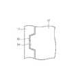
図8は、モールドフレームの従来の射出成形を説明するための模式図である。同図には、モールドフレーム2及びランナー部4が示されている。図示しない金型にはモールドフレーム2の形状を有するキャビティが形成される。キャビティは溶融樹脂がその全体に均一に進入する位置に設けられた複数のゲートを介してランナーに接続される。従来、モールドフレーム2の背面又は前面にゲートを配置して射出成形が行われている。 FIG. 8 is a schematic view for explaining conventional injection molding of a mold frame. In the figure, the
キャビティ及びランナーに注入された樹脂が冷えて固まると図8の上側に示すように、モールドフレーム2とランナー部4とが一体の中間成形品8が金型から取り出される。この中間成形品8をゲートの位置(ゲート部6)で切断して、図8の下側に示すように、モールドフレーム2がランナー部4から切り離される。 When the resin injected into the cavity and the runner cools and hardens, the intermediate molded product 8 in which the
この切断の精度によってはゲート部6の先端がモールドフレーム2側に残ってモールドフレーム2の表面に凸部を生じ得る。そこで、この凸部が当該表面への他の部材の取り付けに支障を来さないように、当該表面を予めゲートの近傍にて後退させ凹部となるように成形し、ゲート残りの凸部が生じても当該凹部から突出しないようにされる。凹部の開口は、例えば、ゲート切断に用いる治具の先端のサイズなどに応じて1mm程度の寸法を必要とする。 Depending on the accuracy of this cutting, the tip of the
液晶表示装置の狭額縁化に伴い、モールドフレームの厚みや枠の太さ(枠幅)の縮小が求められており、近年では例えば、それらは1mm未満になり得る。ゲートをモールドフレームの周上のどこに配置するかは、溶融樹脂がキャビティに同時に、しかも均等に流入するという観点から決定され、ゲートをモールドフレームの厚みや幅が微小な細い部分に配置すべき場合がある。しかし、そのような微細な部分に、上述の凹部を伴うゲートの配置スペースを確保することは容易ではない。また、バックライト装置は薄い形状を有するので基本的にその厚み方向の強度が他の方向より低い。そのため、ゲートの位置をモールドフレームの細い部分の前面又は背面に設定すると、上述の凹部にてモールドフレームの厚みが小さくなり、厚み方向の強度がさらに弱くなるという問題がある。さらに、枠の内側側面には光学シートの縁に設ける突起を受け入れるための凹部がゲート近傍の凹部とは別個に設けられ、この凹部は強度を一層低下させ得る。 With the narrowing of the frame of the liquid crystal display device, reduction of the thickness of the mold frame and the thickness of the frame (frame width) is required. In recent years, for example, they can be less than 1 mm. Where to place the gate on the periphery of the mold frame is determined from the viewpoint that molten resin flows into the cavity simultaneously and evenly, and the gate should be placed in a thin part where the thickness and width of the mold frame are very small There is. However, it is not easy to secure an arrangement space for the gate with the above-described recess in such a fine portion. In addition, since the backlight device has a thin shape, the strength in the thickness direction is basically lower than in other directions. Therefore, when the position of the gate is set to the front or back of the thin part of the mold frame, there is a problem that the thickness of the mold frame is reduced by the above-described recess, and the strength in the thickness direction is further reduced. Furthermore, a recess for receiving a protrusion provided on the edge of the optical sheet is provided on the inner side surface of the frame separately from the recess near the gate, and this recess can further reduce the strength.
本発明は上記問題点を解決するためになされたものであり、モールドフレームの微細化を可能として、一層の狭額縁化がされたバックライト装置及び液晶表示装置を提供することを目的とする。 The present invention has been made to solve the above-described problems, and an object of the present invention is to provide a backlight device and a liquid crystal display device in which the mold frame can be miniaturized and the frame is further narrowed.
本発明に係るバックライト装置は、背面に反射シートを配置された導光板と、前記導光板の光放出面上に配置される、拡散シート又はプリズムシートである少なくとも1枚の光学シートと、内側に前記導光板及び前記光学シートの積層体を収める枠であって、樹脂を注入するゲートを当該枠の内側側面に配して射出成形されるモールドフレームを有し、前記モールドフレームは、前記内側側面が前記ゲートの位置を包含する部分にて後退して形成される凹部であって、当該モールドフレームの厚み方向のうち少なくとも前面側に開いた凹部を有し、少なくとも1枚の前記光学シートは、前記凹部に嵌る突起部を有する。 A backlight device according to the present invention includes a light guide plate having a reflective sheet disposed on the back surface, at least one optical sheet that is a diffusion sheet or a prism sheet disposed on a light emission surface of the light guide plate, and an inner side. A frame for accommodating a laminate of the light guide plate and the optical sheet, and having a mold frame that is injection-molded by arranging a gate for injecting a resin on an inner side surface of the frame, The side surface is a recess formed by retreating at a portion including the position of the gate, and has a recess opened at least on the front side in the thickness direction of the mold frame, and at least one of the optical sheets is And a protrusion that fits into the recess.
本発明の好適な態様は、前記凹部が、前記厚み方向のうち前記前面側のみに開き、前記背面側にはつながっていないバックライト装置である。 The suitable aspect of this invention is a backlight apparatus which the said recessed part opens only in the said front side among the said thickness directions, and is not connected with the said back side.
本発明の他の好適な態様は、前記凹部が、前記内側側面の後退方向に狭くなる線形テーパを有し、前記前面から見て台形形状であるバックライト装置である。 Another preferred aspect of the present invention is the backlight device, wherein the concave portion has a linear taper that becomes narrower in the receding direction of the inner side surface, and has a trapezoidal shape when viewed from the front surface.
本発明に係る液晶表示装置は、上記本発明に係るバックライト装置と、当該バックライト装置の前面に設置される液晶表示パネルを有する。 The liquid crystal display device according to the present invention includes the backlight device according to the present invention and a liquid crystal display panel installed in front of the backlight device.
本発明によれば、モールドフレームのさらなる微細化が可能となり、一層の狭額縁化がされたバックライト装置及び液晶表示装置が実現される。 According to the present invention, the mold frame can be further miniaturized, and a backlight device and a liquid crystal display device with a further narrowed frame can be realized.
以下、本発明の実施の形態(以下実施形態という)について、図面に基づいて説明する。 Hereinafter, embodiments of the present invention (hereinafter referred to as embodiments) will be described with reference to the drawings.
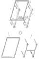
図1は、実施形態に係るバックライト装置10の概略の展開斜視図である。このバックライト装置10はサイドライト方式であり、長方形の枠形状のモールドフレーム12の背面に、反射シート14が貼り付けられる。反射シート14が取り付けられたモールドフレーム12の枠内には、導光板16、拡散シート18、プリズムシート20,22が順番に積層される。モールドフレーム12の前面には、フレーム周に沿って遮光テープ24が貼り付けられる。また、モールドフレーム12の短辺のうち一方は、幅広に形成され、この幅広部分26の背面には固定テープ28が貼り付けられる。 FIG. 1 is a schematic exploded perspective view of a
モールドフレーム12の幅広部分26の背面には、発光ダイオード(Light Emitting Diode:LED)が配列された電子基板(図示せず)が取り付けられる。固定テープ28はこの電子基板をモールドフレーム12に固定する。 An electronic board (not shown) on which light emitting diodes (LEDs) are arranged is attached to the back surface of the
LEDはサイドライト方式の本バックライト装置10の光源である。導光板16は例えば、アクリルで形成され、幅広部分26側の側部からLED光を入射される。入射した光は導光板16内で全反射を繰り返して面状に広がる。導光板16はその各所に伝達された光によって前面側の表面(光放出面)が一様に光るように構成される。 The LED is a light source of the sidelight
反射シート14は、当該シートの縁に予め粘着テープ等の粘着部材を備え、当該粘着部によりモールドフレーム12に固定される。反射シート14は導光板16の裏面から漏れ出る光を反射して導光板16へ戻し、バックライト装置10の発光効率を向上させる。 The
拡散シート18は、光を拡散する樹脂がコーティングされたフィルムである。拡散シート18は導光板16の表面から出射される光を拡散し、発光面内での光強度の均一性を向上させる。 The
プリズムシート20,22はそれぞれ表面に一方向伸びる筋状のプリズムやレンズを成形されたフィルムであり、拡散シート18から前面の様々な方向へ出射される光を面に垂直な方向を中心として集光させ、発光面正面における輝度を向上させる。プリズムシート20,22はそれぞれプリズム等の延在方向とは直交する方向に対する集光を行い、集光方向が異なる2枚のプリズムシート20,22を重ねることで二次元的な集光が実現される。 Each of the
図2は、実施形態に係る液晶表示装置30の垂直断面の一部を示す模式的な断面図である。液晶表示装置30は、バックライト装置10の前面に液晶表示パネル32を配置される。遮光テープ24は、液晶表示装置30においてバックライト装置10と液晶表示パネル32とを接着する粘着部材である。この接着部分からバックライト装置10の光が漏れ出て液晶表示装置30のコントラスト低下等の問題を生じないように、当該粘着部材として遮光性を有するものを用いる。 FIG. 2 is a schematic cross-sectional view showing a part of a vertical cross section of the liquid
なお、液晶表示パネル32は、透明な一対のガラス基板、その間に挟まれた液晶、及びその他の構成要素からなるが、図2においてその構造は省略している。液晶表示パネル32は、画素毎に液晶の配向を制御して、バックライト装置10から入射した光に対する透過率を変えることにより画面に画像を形成する。 The liquid
モールドフレーム12は上述のように、長方形の枠形状に形成され、枠内に導光板16及び光学シート(拡散シート18、プリズムシート20,22)の積層体を収める。モールドフレーム12は、金型を用いて樹脂を射出成形して形成される。図3は、モールドフレーム12の射出成形を説明するための模式図である。金型にはモールドフレーム12に対応したキャビティが形成され、キャビティは注入口(ゲート)にて、樹脂からなるランナーに接続される。ランナー、ゲートを介してキャビティに溶融樹脂が注入され、当該樹脂が冷えて固まると金型が取り外される。図3の上側はこの金型を取り外した状態を表しており、キャビティにより成形されたモールドフレーム12と、樹脂が注入されたランナーからなるランナー部40とが一体となった中間成形品42が得られる。 As described above, the
この中間成形品42において、ゲート部44がゲートの位置に対応する。ゲートは、溶融樹脂がキャビティの全体に均一に進入する位置に設けられる。均一な注入を実現するためにゲートは複数箇所に設けることができる。本実施形態では4つのゲートが設けられ、長方形の枠状のモールドフレーム12において短辺より長辺にて多くの樹脂を要することに対応して、各長辺に2つのゲートが配置される。また、2つの短辺のうち幅広部分26の方がもう一方の細い短辺46より多くの樹脂注入を要することに対応して、幅広部分26と最寄りのゲートとの距離は細い短辺46と最寄りのゲートとの距離より短く設定されている。 In the intermediate molded
従来技術で説明した構成と異なり、これらのゲートはモールドフレーム12の枠の内側側面に配置される。例えば、ランナーは、モールドフレーム12の短辺に平行に延在され、その両端を2つの長辺上の対向する2つのゲートに接続される部分48a,48bと、これら部分48a,48bの中央部分に両端を接続され、長辺に平行に延在される部分48cとで“H”型に構成される。溶融樹脂は部分48cの中央から注入され、部分48cから部分48a,48bにそれぞれ流入し、さらにゲートを介してキャビティに注入される。 Unlike the configuration described in the prior art, these gates are arranged on the inner side surface of the frame of the
中間成形品42はゲート部44にて切断され、図3の下側に示すように、モールドフレーム12がランナー部40から切り離される。モールドフレーム12は、ゲートの位置を包含する部分にて内側側面が後退して形成される凹部50を有する。この凹部50は、従来技術と同様、モールドフレーム12にゲート痕として生じ得る凸部への対策として設けられる。 The intermediate molded
凹部50は、モールドフレーム12の厚み方向のうち少なくとも前面側に開いている。つまり、モールドフレーム12の厚み方向に沿って、凹部50とモールドフレーム12の前面(上面)との間には壁は存在せず、凹部50の底面をなす後退した内側側面はモールドフレーム12の上面に達する。よって、モールドフレーム12の上面には凹部50が現れる。 The
図4は、光学シート52が枠内に配置されたモールドフレーム12の模式的な平面図である。同図はモールドフレーム12の上面に現れる凹部50をわかりやすく示している。図4に示すように、モールドフレーム12内に配置される光学シート52(拡散シート18、プリズムシート20,22)は、凹部50に嵌る突起部54を有する。凹部50が前面側に開いているので、光学シート52をモールドフレーム12内に置けば、突起部54は凹部50に入る。 FIG. 4 is a schematic plan view of the
バックライト装置10において光学シート52はモールドフレーム12内に基本的に置かれているだけであり、接着等の手段で固定されていない。そのためバックライト装置10は、前面に液晶表示パネル32を取り付けられていない状態では、光学シート52が搬送中の振動などによってモールドフレーム12から飛び出して脱落する可能性を有している。凹部50に入った突起部54は、当該突起部54がない場合と比べて、この光学シート52の脱落を起こしにくくする。また、プリズムシート20,22は反ってその端部が浮くことがあるが、突起部54を設けることで端部をモールドフレーム12から浮きにくくすることができる。なお、モールドフレーム12と光学シート52との間には、各部材の熱収縮の相違や加工精度を考慮して設けられる微小な間隙が存在していても良い。 In the
突起部54は、図4に示すように各凹部50の位置に設けてもよいし、一部の凹部50の位置だけに設けてもよい。例えば、プリズムシート20,22の反りが特定の対角線方向において生じる場合には、その対角線上の2つの角に近い凹部50の位置だけに突起部54を設けることができる。 As shown in FIG. 4, the
また、突起部54は全ての光学シート52に対して設けてもよいし、一部のシートだけに設けてもよい。例えば、光学シート52のうち一番上に位置するプリズムシート22だけに突起部54を設けて、その下の拡散シート18及びプリズムシート20の脱落防止も図ることができる。 Further, the
凹部50は上述したように射出成形に伴って形成され、その位置は溶融樹脂が好適に注入されるように設計される。バックライト装置10では当該凹部50を突起部54を受け入れるために活用する。これにより、突起部54を嵌めるための凹部を別途、モールドフレーム12に形成する必要がなくなる。すなわち、凹部にてモールドフレーム12が細くなることによるバックライト装置10の強度低下を少なくしつつ、突起部54を設けて光学シート52の脱落防止を図ることができる。 As described above, the
図5はモールドフレーム12の凹部50が形成された部分の模式的な斜視図である。図5に示す凹部50は、モールドフレーム12の厚み方向のうち前面側のみに開き、背面側にはつながっていない。この凹部50でのモールドフレーム12の断面は図2に示されており、同図に示すように当該凹部50はモールドフレーム12の内側前面の角をL字型に切り欠いた形状をなす。なお、図2のバックライト装置10の断面は、図4では例えば、II−II線の位置に対応する。 FIG. 5 is a schematic perspective view of a portion of the
このようにモールドフレーム12の厚み方向の一部を凹部50にせずに本来の幅のまま残すことにより、モールドフレーム12の強度低下を少なくすることができる。 Thus, by leaving a part in the thickness direction of the
図6はモールドフレーム12の凹部50が形成された部分の他の例を示す模式的な斜視図である。図6に示す凹部50は、モールドフレーム12の厚み方向の背面側にも開いている。つまり、凹部50の底面はモールドフレーム12の前面から背面までつながっている。この凹部50は図5の凹部50よりもモールドフレーム12の幅方向の強度は低下する。しかし、同様の大きさの凹部をモールドフレーム12の前面や背面に設けることが、バックライト装置10の短辺方向や長辺方向に比べて弱い厚み方向の強度をさらに低下させることに比べれば、図6の凹部50がバックライト装置10の強度に与える影響は少ない。 FIG. 6 is a schematic perspective view showing another example of the portion of the
ここまで図に例示した凹部50は前面から見ると基本的には矩形であった。つまり、凹部50の底面と凹部50両側のモールドフレーム12の内側側面とはそれぞれに対して垂直であり、モールドフレーム12の長辺方向に関する凹部50の間口寸法と底面寸法とは基本的に同じとしていた。しかし、間口寸法と底面寸法とは異なってもよい。 The
図7はモールドフレーム12の凹部50が形成された部分の他の例を示す模式的な平面図である。図7に示す凹部50は、内側側面の後退方向に狭くなる線形テーパを有し、前面から見て台形形状である。つまり、間口寸法より底面寸法が小さくなるように形成されている。このような順テーパの凹部50は射出成形にて容易に形成できる。光学シート52の突起部54は当該凹部50に適合するテーパを付すことができる。この光学シート52の形状では、突起部54の根本の屈曲(入り隅)部分が鈍角となり、光学シート52が当該部分から内側へ裂けにくくなる。なお、当該裂けの発生を抑制するために、当該部分を円弧等のよりなめらかな形状としてもよい。 FIG. 7 is a schematic plan view showing another example of a portion of the
モールドフレーム12の内側側面にゲートを設けると、凹部50がバックライト装置10の外面に現れない。このことは、バックライト装置10の美観を損ねないだけでなく、バックライト装置10やこれを用いた液晶表示装置30を部品として他の装置に組み込む際にモールドフレーム12の外側側面を接着スペースとして利用したり、組み立てのための構造をモールドフレーム12の外側側面に別途形成する際の設計の自由度を確保できる。また、モールドフレーム12の内側側面にゲートを配置したことに加え、ランナーを側方からゲートに接続し、かつ当該ゲートに対応して設ける凹部50を前面側に開いた形状としたことにより、中間成形品42を図3に示したように分割する際に、ゲート切断に用いる治具の刃先を前面側から直線的に差し込んでゲートの根本(モールドフレーム12側の端部)に当てることができる。この刃先の前面から背面へ向かう挿入方向は各凹部50にて共通であり、各凹部50での切断を同時に行うことが容易である。 When the gate is provided on the inner side surface of the
ちなみに、携帯電話等の小型の装置の部品として上述の本発明に係るバックライト装置10、液晶表示装置30を用いることができ、そのような小型の装置では、モールドフレーム12の厚みや枠幅は1mm程度、もしくはそれ以下となり得る。そのような枠幅の細いモールドフレーム12では凹部50の深さは当然のことながら枠幅未満の浅いものとなるが、強度確保の観点からはできるだけ浅くすることが好適である。凹部50の間口寸法(又は底面寸法)は、切断治具の刃先が入る大きさである必要があるが、当該治具の刃先を微細にして、当該間口寸法をできるだけ小さくすることが強度上好適である。例えば、間口寸法は1mm程度にすることが可能である。 Incidentally, the
10 バックライト装置、12 モールドフレーム、14 反射シート、16 導光板、18 拡散シート、20,22 プリズムシート、24 遮光テープ、28 固定テープ、30 液晶表示装置、32 液晶表示パネル、40 ランナー部、42 中間成形品、44 ゲート部、50 凹部、52 光学シート、54 突起部。 DESCRIPTION OF
Claims (5)
Translated fromJapanese背面に反射シートを配置された導光板と、
前記導光板の光放出面上に配置される、拡散シート又はプリズムシートである少なくとも1枚の光学シートと、
前記導光板及び前記光学シートの積層体の外周を取り囲んで当該積層体を内側に収める枠であって、樹脂を注入するゲートを当該枠の内側側面に配して射出成形されるモールドフレームと、を有し、
前記モールドフレームは、前記内側側面が前記ゲートの位置を包含する部分にて後退して形成される凹部であって、当該モールドフレームの厚み方向のうち前面側のみに開き、背面側にはつながっていない凹部を有し、
少なくとも1枚の前記光学シートは、前記凹部に嵌る突起部を有し、
前記凹部は、前記前面側に向いた面であって前記光学シートの前記突起部が対向配置される面を有すること、
を特徴とするバックライト装置。A backlight device installed on the back of the liquid crystal display panel,
A light guide plate having a reflective sheet disposed on the back;
At least one optical sheet, which is a diffusion sheet or a prism sheet, disposed on the light emission surface of the light guide plate;
A frame to accommodatethe laminate surrounds the outer periphery of thefront Kishirube light plate and the stack of the optical sheeton the inside, and a mold frame gate for injecting a resin disposed inside the side surface of the frame is injection molded Have
The mold frame is a recess formed by retreating the inner side surface at a portion including the position of the gate,and opens only on the front side in the thickness direction of the mold frame,and is connected to the back side. Hasno recess,
At least one of the optical sheet,have a protrusion that fits in therecess,
The recess, that the protrusion of the optical sheet to a surface facing to the front side is closed a surface disposed opposite,
A backlight device characterized by.
前記モールドフレームは前記凹部にて前記導光板に対応した厚みを有すること、を特徴とするバックライト装置。The backlight device according to claim 1, wherein the mold frame has a thickness corresponding to the light guide plate at the concave portion.
前記凹部は、前記内側側面の後退方向に狭くなる線形テーパを有し、前記前面から見て台形形状であること、を特徴とするバックライト装置。The backlight device according to claim 1,
The said recessed part has a linear taper which becomes narrow in the retraction direction of the said inner side surface, and is a trapezoid shape seeing from the said front surface, The backlight apparatus characterized by the above-mentioned.
前記枠は2つの短辺と2つの長辺を有する長方形の形状であり、第1の前記短辺よりも第2の前記短辺において幅広に形成され、The frame has a rectangular shape having two short sides and two long sides, and is formed wider at the second short side than at the first short side,
前記各長辺の2箇所に第1の前記凹部と第2の前記凹部とが形成され、The first concave portion and the second concave portion are formed at two locations on each long side,
前記第1の凹部は前記第2の短辺よりも前記第1の短辺寄りに形成され、The first recess is formed closer to the first short side than the second short side,
前記第2の凹部は前記第1の短辺よりも前記第2の短辺寄りに形成され、The second recess is formed closer to the second short side than the first short side,
前記第1の凹部と前記第1の短辺との距離は、前記第2の凹部と前記第2の短辺との距離よりも短いこと、The distance between the first recess and the first short side is shorter than the distance between the second recess and the second short side;
を特徴とするバックライト装置。A backlight device characterized by.
当該バックライト装置の前面に設置される液晶表示パネルと、
を有する液晶表示装置。The backlight device according to any one of claims 1 to4 ,
A liquid crystal display panel installed in front of the backlight device;
A liquid crystal display device.
Priority Applications (6)
| Application Number | Priority Date | Filing Date | Title |
|---|---|---|---|
| JP2010227330AJP5211131B2 (en) | 2010-10-07 | 2010-10-07 | Backlight device and liquid crystal display device |
| TW100134850ATWI474084B (en) | 2010-10-07 | 2011-09-27 | A backlight device and a liquid crystal display device |
| CN201110305519.7ACN102444842B (en) | 2010-10-07 | 2011-09-30 | Backlight device and liquid crystal display device |
| CN2011203833339UCN202691755U (en) | 2010-10-07 | 2011-09-30 | Backlight device and liquid crystal display device |
| US13/253,178US20120086890A1 (en) | 2010-10-07 | 2011-10-05 | Backlight device and liquid crystal display device |
| KR1020110101790AKR101290971B1 (en) | 2010-10-07 | 2011-10-06 | Back-light device and liquid crystal display device |
Applications Claiming Priority (1)
| Application Number | Priority Date | Filing Date | Title |
|---|---|---|---|
| JP2010227330AJP5211131B2 (en) | 2010-10-07 | 2010-10-07 | Backlight device and liquid crystal display device |
Publications (2)
| Publication Number | Publication Date |
|---|---|
| JP2012084253A JP2012084253A (en) | 2012-04-26 |
| JP5211131B2true JP5211131B2 (en) | 2013-06-12 |
Family
ID=45924865
Family Applications (1)
| Application Number | Title | Priority Date | Filing Date |
|---|---|---|---|
| JP2010227330AActiveJP5211131B2 (en) | 2010-10-07 | 2010-10-07 | Backlight device and liquid crystal display device |
Country Status (5)
| Country | Link |
|---|---|
| US (1) | US20120086890A1 (en) |
| JP (1) | JP5211131B2 (en) |
| KR (1) | KR101290971B1 (en) |
| CN (2) | CN202691755U (en) |
| TW (1) | TWI474084B (en) |
Families Citing this family (14)
| Publication number | Priority date | Publication date | Assignee | Title |
|---|---|---|---|---|
| JP5211131B2 (en)* | 2010-10-07 | 2013-06-12 | 株式会社ジャパンディスプレイイースト | Backlight device and liquid crystal display device |
| US20130107168A1 (en)* | 2011-11-01 | 2013-05-02 | Shenzhen China Star Optoelectronics Technology Co., Ltd. | Backlight module and liquid crystal display |
| EP2713200B1 (en)* | 2012-09-26 | 2015-10-28 | LG Display Co., Ltd. | Liquid crystal display device |
| TWI509314B (en)* | 2013-10-23 | 2015-11-21 | Coretronic Corp | Display device |
| JP2015090823A (en)* | 2013-11-07 | 2015-05-11 | Nltテクノロジー株式会社 | Backlight unit and liquid crystal display device using the same |
| KR20150141237A (en) | 2014-06-09 | 2015-12-18 | 삼성디스플레이 주식회사 | Liquid crystal display |
| KR102164261B1 (en)* | 2014-08-08 | 2020-10-13 | 엘지디스플레이 주식회사 | Liquid crystal display device having means for fixing of optical sheets |
| CN104614898B (en)* | 2015-02-12 | 2018-05-01 | 京东方科技集团股份有限公司 | A kind of display device |
| KR102394030B1 (en)* | 2015-03-31 | 2022-05-06 | 삼성디스플레이 주식회사 | Prism plate, display device having the same, and method of manufacturing prism plate |
| CN107403856B (en)* | 2016-05-19 | 2019-10-22 | 华为终端有限公司 | A kind of LED and its manufacturing method and electronic equipment using the LED |
| US10824010B2 (en) | 2018-03-05 | 2020-11-03 | Huizhou China Star Optoelectronics Technology Co., Ltd. | Backlight module and display apparatus |
| CN108303827A (en)* | 2018-03-05 | 2018-07-20 | 惠州市华星光电技术有限公司 | A kind of backlight module and display device |
| KR102680672B1 (en)* | 2018-10-10 | 2024-07-02 | 삼성디스플레이 주식회사 | Liquid crystal display device and method of manufacturing the same |
| CN112578590B (en) | 2019-09-29 | 2022-04-29 | 京东方科技集团股份有限公司 | Backlight module and display device |
Family Cites Families (17)
| Publication number | Priority date | Publication date | Assignee | Title |
|---|---|---|---|---|
| JP3411448B2 (en)* | 1996-07-03 | 2003-06-03 | 沖電気工業株式会社 | Resin sealing mold for semiconductor element and method for manufacturing semiconductor device |
| JPH1186489A (en)* | 1997-09-16 | 1999-03-30 | Tdk Corp | Disk cartridge |
| US6108298A (en)* | 1997-04-15 | 2000-08-22 | Tdk Corporation | Disc cartridge |
| KR100739527B1 (en)* | 2000-10-13 | 2007-07-13 | 삼성전자주식회사 | Backlight Unit of Liquid Crystal Display |
| TWM268608U (en)* | 2004-12-10 | 2005-06-21 | Innolux Display Corp | Back light module |
| JP5061277B2 (en)* | 2005-11-21 | 2012-10-31 | 株式会社ジャパンディスプレイイースト | Display device |
| US7626747B2 (en)* | 2006-06-02 | 2009-12-01 | Panasonic Corporation | Liquid crystal display apparatus |
| JP4872676B2 (en)* | 2006-06-02 | 2012-02-08 | パナソニック株式会社 | Liquid crystal display |
| KR20080011983A (en)* | 2006-08-02 | 2008-02-11 | 삼성전자주식회사 | Back light assembly and liquid crystal display device having same |
| KR20080035043A (en)* | 2006-10-18 | 2008-04-23 | 삼성전자주식회사 | Back light assembly and display device having same |
| JP2008293902A (en)* | 2007-05-28 | 2008-12-04 | Funai Electric Co Ltd | Backlight device and display device using it |
| JP2008305576A (en)* | 2007-06-05 | 2008-12-18 | Toshiba Matsushita Display Technology Co Ltd | Lighting unit, and liquid crystal display device with the same |
| JP2009163964A (en)* | 2007-12-29 | 2009-07-23 | Citizen Finetech Miyota Co Ltd | Lighting device |
| JP2009181068A (en)* | 2008-01-31 | 2009-08-13 | Toppan Printing Co Ltd | Optical sheet, backlight device, display device, and optical sheet manufacturing method |
| KR20090100117A (en)* | 2008-03-19 | 2009-09-23 | 삼성전자주식회사 | Backlight unit and liquid crystal display including the same |
| KR101515462B1 (en)* | 2008-11-13 | 2015-05-06 | 삼성디스플레이 주식회사 | Liquid crystal display device and method of assembling the same |
| JP5211131B2 (en)* | 2010-10-07 | 2013-06-12 | 株式会社ジャパンディスプレイイースト | Backlight device and liquid crystal display device |
- 2010
- 2010-10-07JPJP2010227330Apatent/JP5211131B2/enactiveActive
- 2011
- 2011-09-27TWTW100134850Apatent/TWI474084B/enactive
- 2011-09-30CNCN2011203833339Upatent/CN202691755U/ennot_activeExpired - Lifetime
- 2011-09-30CNCN201110305519.7Apatent/CN102444842B/enactiveActive
- 2011-10-05USUS13/253,178patent/US20120086890A1/ennot_activeAbandoned
- 2011-10-06KRKR1020110101790Apatent/KR101290971B1/enactiveActive
Also Published As
| Publication number | Publication date |
|---|---|
| JP2012084253A (en) | 2012-04-26 |
| TWI474084B (en) | 2015-02-21 |
| KR20120036283A (en) | 2012-04-17 |
| CN102444842B (en) | 2015-03-18 |
| TW201219928A (en) | 2012-05-16 |
| US20120086890A1 (en) | 2012-04-12 |
| CN102444842A (en) | 2012-05-09 |
| CN202691755U (en) | 2013-01-23 |
| KR101290971B1 (en) | 2013-07-30 |
Similar Documents
| Publication | Publication Date | Title |
|---|---|---|
| JP5211131B2 (en) | Backlight device and liquid crystal display device | |
| JP4993096B2 (en) | Planar illumination device, transparent resin substrate thereof, and injection molding method of transparent resin substrate | |
| US9927643B2 (en) | Liquid crystal display device and method for manufacturing the same | |
| JP5436935B2 (en) | Liquid crystal display | |
| US20140354918A1 (en) | Surface light source device and frame used therein | |
| KR20110003777A (en) | Optical assembly, backlight unit and display device having same | |
| US20110109836A1 (en) | Illumination device and liquid crystal display device | |
| KR101630342B1 (en) | Liquid crystal display device and mathod for manufacturing the same | |
| JP2013026110A (en) | Lighting system, liquid crystal display device and electronic equipment | |
| KR20150066847A (en) | Material for controlling luminous flux, light emitting device and display device | |
| KR101922062B1 (en) | Liquid Crystal Display device and Method for manufacturing the same | |
| KR102376821B1 (en) | Liquid crystal display module and liquid crystal display apparatus using the same | |
| KR20150066846A (en) | Optical element and light emitting device including the same | |
| US20140192554A1 (en) | Illumination device and display device provided therewith | |
| KR20110027185A (en) | Light guide plate and backlight unit having same | |
| JP2017021228A (en) | Display device | |
| KR102296755B1 (en) | Light guide panel holder and back light unit and liquid crystal display apparatus using the same | |
| KR20170014400A (en) | Liquid crystal display module and liquid crystal display apparatus using the same | |
| KR20150026479A (en) | Backlight unit and liquid crystal display device usint the same | |
| KR101047704B1 (en) | Backlight unit and display device with optical assembly | |
| KR101064088B1 (en) | Backlight unit and display device with optical assembly | |
| CN117425852A (en) | Planar lighting device | |
| KR102727942B1 (en) | Backlight unit and liquid crystal display device having the same | |
| US20200379289A1 (en) | Backlight module and liquid crystal module | |
| KR102396019B1 (en) | Backlight Unit And Liquid Crystal Display Device Using The Same |
Legal Events
| Date | Code | Title | Description |
|---|---|---|---|
| A977 | Report on retrieval | Free format text:JAPANESE INTERMEDIATE CODE: A971007 Effective date:20120928 | |
| A131 | Notification of reasons for refusal | Free format text:JAPANESE INTERMEDIATE CODE: A131 Effective date:20121009 | |
| A521 | Request for written amendment filed | Free format text:JAPANESE INTERMEDIATE CODE: A523 Effective date:20121205 | |
| TRDD | Decision of grant or rejection written | ||
| A01 | Written decision to grant a patent or to grant a registration (utility model) | Free format text:JAPANESE INTERMEDIATE CODE: A01 Effective date:20130212 | |
| A61 | First payment of annual fees (during grant procedure) | Free format text:JAPANESE INTERMEDIATE CODE: A61 Effective date:20130225 | |
| FPAY | Renewal fee payment (event date is renewal date of database) | Free format text:PAYMENT UNTIL: 20160301 Year of fee payment:3 | |
| R150 | Certificate of patent or registration of utility model | Ref document number:5211131 Country of ref document:JP Free format text:JAPANESE INTERMEDIATE CODE: R150 Free format text:JAPANESE INTERMEDIATE CODE: R150 | |
| R250 | Receipt of annual fees | Free format text:JAPANESE INTERMEDIATE CODE: R250 | |
| R250 | Receipt of annual fees | Free format text:JAPANESE INTERMEDIATE CODE: R250 | |
| R250 | Receipt of annual fees | Free format text:JAPANESE INTERMEDIATE CODE: R250 | |
| R250 | Receipt of annual fees | Free format text:JAPANESE INTERMEDIATE CODE: R250 | |
| R250 | Receipt of annual fees | Free format text:JAPANESE INTERMEDIATE CODE: R250 | |
| R250 | Receipt of annual fees | Free format text:JAPANESE INTERMEDIATE CODE: R250 | |
| S531 | Written request for registration of change of domicile | Free format text:JAPANESE INTERMEDIATE CODE: R313531 | |
| S533 | Written request for registration of change of name | Free format text:JAPANESE INTERMEDIATE CODE: R313533 | |
| R350 | Written notification of registration of transfer | Free format text:JAPANESE INTERMEDIATE CODE: R350 | |
| R250 | Receipt of annual fees | Free format text:JAPANESE INTERMEDIATE CODE: R250 | |
| R250 | Receipt of annual fees | Free format text:JAPANESE INTERMEDIATE CODE: R250 | |
| R250 | Receipt of annual fees | Free format text:JAPANESE INTERMEDIATE CODE: R250 | |
| R250 | Receipt of annual fees | Free format text:JAPANESE INTERMEDIATE CODE: R250 | |
| S111 | Request for change of ownership or part of ownership | Free format text:JAPANESE INTERMEDIATE CODE: R313113 | |
| R350 | Written notification of registration of transfer | Free format text:JAPANESE INTERMEDIATE CODE: R350 |