JP5207659B2 - Semiconductor device - Google Patents
Semiconductor deviceDownload PDFInfo
- Publication number
- JP5207659B2 JP5207659B2JP2007134927AJP2007134927AJP5207659B2JP 5207659 B2JP5207659 B2JP 5207659B2JP 2007134927 AJP2007134927 AJP 2007134927AJP 2007134927 AJP2007134927 AJP 2007134927AJP 5207659 B2JP5207659 B2JP 5207659B2
- Authority
- JP
- Japan
- Prior art keywords
- electrode
- ball
- electrode pad
- printed wiring
- wiring board
- Prior art date
- Legal status (The legal status is an assumption and is not a legal conclusion. Google has not performed a legal analysis and makes no representation as to the accuracy of the status listed.)
- Expired - Fee Related
Links
Images


Classifications
- H—ELECTRICITY
- H05—ELECTRIC TECHNIQUES NOT OTHERWISE PROVIDED FOR
- H05K—PRINTED CIRCUITS; CASINGS OR CONSTRUCTIONAL DETAILS OF ELECTRIC APPARATUS; MANUFACTURE OF ASSEMBLAGES OF ELECTRICAL COMPONENTS
- H05K1/00—Printed circuits
- H05K1/02—Details
- H05K1/11—Printed elements for providing electric connections to or between printed circuits
- H05K1/111—Pads for surface mounting, e.g. lay-out
- H—ELECTRICITY
- H01—ELECTRIC ELEMENTS
- H01L—SEMICONDUCTOR DEVICES NOT COVERED BY CLASS H10
- H01L23/00—Details of semiconductor or other solid state devices
- H01L23/12—Mountings, e.g. non-detachable insulating substrates
- H—ELECTRICITY
- H01—ELECTRIC ELEMENTS
- H01L—SEMICONDUCTOR DEVICES NOT COVERED BY CLASS H10
- H01L23/00—Details of semiconductor or other solid state devices
- H01L23/48—Arrangements for conducting electric current to or from the solid state body in operation, e.g. leads, terminal arrangements ; Selection of materials therefor
- H01L23/488—Arrangements for conducting electric current to or from the solid state body in operation, e.g. leads, terminal arrangements ; Selection of materials therefor consisting of soldered or bonded constructions
- H01L23/498—Leads, i.e. metallisations or lead-frames on insulating substrates, e.g. chip carriers
- H01L23/49811—Additional leads joined to the metallisation on the insulating substrate, e.g. pins, bumps, wires, flat leads
- H01L23/49816—Spherical bumps on the substrate for external connection, e.g. ball grid arrays [BGA]
- H—ELECTRICITY
- H01—ELECTRIC ELEMENTS
- H01L—SEMICONDUCTOR DEVICES NOT COVERED BY CLASS H10
- H01L24/00—Arrangements for connecting or disconnecting semiconductor or solid-state bodies; Methods or apparatus related thereto
- H01L24/01—Means for bonding being attached to, or being formed on, the surface to be connected, e.g. chip-to-package, die-attach, "first-level" interconnects; Manufacturing methods related thereto
- H01L24/02—Bonding areas ; Manufacturing methods related thereto
- H01L24/04—Structure, shape, material or disposition of the bonding areas prior to the connecting process
- H01L24/06—Structure, shape, material or disposition of the bonding areas prior to the connecting process of a plurality of bonding areas
- H—ELECTRICITY
- H01—ELECTRIC ELEMENTS
- H01L—SEMICONDUCTOR DEVICES NOT COVERED BY CLASS H10
- H01L24/00—Arrangements for connecting or disconnecting semiconductor or solid-state bodies; Methods or apparatus related thereto
- H01L24/01—Means for bonding being attached to, or being formed on, the surface to be connected, e.g. chip-to-package, die-attach, "first-level" interconnects; Manufacturing methods related thereto
- H01L24/10—Bump connectors ; Manufacturing methods related thereto
- H01L24/15—Structure, shape, material or disposition of the bump connectors after the connecting process
- H01L24/17—Structure, shape, material or disposition of the bump connectors after the connecting process of a plurality of bump connectors
- H—ELECTRICITY
- H01—ELECTRIC ELEMENTS
- H01L—SEMICONDUCTOR DEVICES NOT COVERED BY CLASS H10
- H01L25/00—Assemblies consisting of a plurality of semiconductor or other solid state devices
- H01L25/03—Assemblies consisting of a plurality of semiconductor or other solid state devices all the devices being of a type provided for in a single subclass of subclasses H10B, H10D, H10F, H10H, H10K or H10N, e.g. assemblies of rectifier diodes
- H01L25/10—Assemblies consisting of a plurality of semiconductor or other solid state devices all the devices being of a type provided for in a single subclass of subclasses H10B, H10D, H10F, H10H, H10K or H10N, e.g. assemblies of rectifier diodes the devices having separate containers
- H01L25/105—Assemblies consisting of a plurality of semiconductor or other solid state devices all the devices being of a type provided for in a single subclass of subclasses H10B, H10D, H10F, H10H, H10K or H10N, e.g. assemblies of rectifier diodes the devices having separate containers the devices being integrated devices of class H10
- H—ELECTRICITY
- H05—ELECTRIC TECHNIQUES NOT OTHERWISE PROVIDED FOR
- H05K—PRINTED CIRCUITS; CASINGS OR CONSTRUCTIONAL DETAILS OF ELECTRIC APPARATUS; MANUFACTURE OF ASSEMBLAGES OF ELECTRICAL COMPONENTS
- H05K1/00—Printed circuits
- H05K1/02—Details
- H05K1/14—Structural association of two or more printed circuits
- H05K1/141—One or more single auxiliary printed circuits mounted on a main printed circuit, e.g. modules, adapters
- H—ELECTRICITY
- H05—ELECTRIC TECHNIQUES NOT OTHERWISE PROVIDED FOR
- H05K—PRINTED CIRCUITS; CASINGS OR CONSTRUCTIONAL DETAILS OF ELECTRIC APPARATUS; MANUFACTURE OF ASSEMBLAGES OF ELECTRICAL COMPONENTS
- H05K3/00—Apparatus or processes for manufacturing printed circuits
- H05K3/30—Assembling printed circuits with electric components, e.g. with resistor
- H05K3/32—Assembling printed circuits with electric components, e.g. with resistor electrically connecting electric components or wires to printed circuits
- H05K3/34—Assembling printed circuits with electric components, e.g. with resistor electrically connecting electric components or wires to printed circuits by soldering
- H05K3/341—Surface mounted components
- H05K3/3431—Leadless components
- H05K3/3436—Leadless components having an array of bottom contacts, e.g. pad grid array or ball grid array components
- H—ELECTRICITY
- H01—ELECTRIC ELEMENTS
- H01L—SEMICONDUCTOR DEVICES NOT COVERED BY CLASS H10
- H01L2224/00—Indexing scheme for arrangements for connecting or disconnecting semiconductor or solid-state bodies and methods related thereto as covered by H01L24/00
- H01L2224/01—Means for bonding being attached to, or being formed on, the surface to be connected, e.g. chip-to-package, die-attach, "first-level" interconnects; Manufacturing methods related thereto
- H01L2224/02—Bonding areas; Manufacturing methods related thereto
- H01L2224/04—Structure, shape, material or disposition of the bonding areas prior to the connecting process
- H01L2224/0401—Bonding areas specifically adapted for bump connectors, e.g. under bump metallisation [UBM]
- H—ELECTRICITY
- H01—ELECTRIC ELEMENTS
- H01L—SEMICONDUCTOR DEVICES NOT COVERED BY CLASS H10
- H01L2224/00—Indexing scheme for arrangements for connecting or disconnecting semiconductor or solid-state bodies and methods related thereto as covered by H01L24/00
- H01L2224/01—Means for bonding being attached to, or being formed on, the surface to be connected, e.g. chip-to-package, die-attach, "first-level" interconnects; Manufacturing methods related thereto
- H01L2224/02—Bonding areas; Manufacturing methods related thereto
- H01L2224/04—Structure, shape, material or disposition of the bonding areas prior to the connecting process
- H01L2224/06—Structure, shape, material or disposition of the bonding areas prior to the connecting process of a plurality of bonding areas
- H01L2224/0601—Structure
- H01L2224/0603—Bonding areas having different sizes, e.g. different heights or widths
- H—ELECTRICITY
- H01—ELECTRIC ELEMENTS
- H01L—SEMICONDUCTOR DEVICES NOT COVERED BY CLASS H10
- H01L2224/00—Indexing scheme for arrangements for connecting or disconnecting semiconductor or solid-state bodies and methods related thereto as covered by H01L24/00
- H01L2224/01—Means for bonding being attached to, or being formed on, the surface to be connected, e.g. chip-to-package, die-attach, "first-level" interconnects; Manufacturing methods related thereto
- H01L2224/10—Bump connectors; Manufacturing methods related thereto
- H01L2224/12—Structure, shape, material or disposition of the bump connectors prior to the connecting process
- H01L2224/13—Structure, shape, material or disposition of the bump connectors prior to the connecting process of an individual bump connector
- H01L2224/13001—Core members of the bump connector
- H01L2224/13099—Material
- H—ELECTRICITY
- H01—ELECTRIC ELEMENTS
- H01L—SEMICONDUCTOR DEVICES NOT COVERED BY CLASS H10
- H01L2224/00—Indexing scheme for arrangements for connecting or disconnecting semiconductor or solid-state bodies and methods related thereto as covered by H01L24/00
- H01L2224/01—Means for bonding being attached to, or being formed on, the surface to be connected, e.g. chip-to-package, die-attach, "first-level" interconnects; Manufacturing methods related thereto
- H01L2224/10—Bump connectors; Manufacturing methods related thereto
- H01L2224/12—Structure, shape, material or disposition of the bump connectors prior to the connecting process
- H01L2224/14—Structure, shape, material or disposition of the bump connectors prior to the connecting process of a plurality of bump connectors
- H01L2224/1401—Structure
- H01L2224/1403—Bump connectors having different sizes, e.g. different diameters, heights or widths
- H—ELECTRICITY
- H01—ELECTRIC ELEMENTS
- H01L—SEMICONDUCTOR DEVICES NOT COVERED BY CLASS H10
- H01L2224/00—Indexing scheme for arrangements for connecting or disconnecting semiconductor or solid-state bodies and methods related thereto as covered by H01L24/00
- H01L2224/01—Means for bonding being attached to, or being formed on, the surface to be connected, e.g. chip-to-package, die-attach, "first-level" interconnects; Manufacturing methods related thereto
- H01L2224/10—Bump connectors; Manufacturing methods related thereto
- H01L2224/15—Structure, shape, material or disposition of the bump connectors after the connecting process
- H01L2224/16—Structure, shape, material or disposition of the bump connectors after the connecting process of an individual bump connector
- H01L2224/161—Disposition
- H01L2224/16151—Disposition the bump connector connecting between a semiconductor or solid-state body and an item not being a semiconductor or solid-state body, e.g. chip-to-substrate, chip-to-passive
- H01L2224/16221—Disposition the bump connector connecting between a semiconductor or solid-state body and an item not being a semiconductor or solid-state body, e.g. chip-to-substrate, chip-to-passive the body and the item being stacked
- H01L2224/16225—Disposition the bump connector connecting between a semiconductor or solid-state body and an item not being a semiconductor or solid-state body, e.g. chip-to-substrate, chip-to-passive the body and the item being stacked the item being non-metallic, e.g. insulating substrate with or without metallisation
- H—ELECTRICITY
- H01—ELECTRIC ELEMENTS
- H01L—SEMICONDUCTOR DEVICES NOT COVERED BY CLASS H10
- H01L2225/00—Details relating to assemblies covered by the group H01L25/00 but not provided for in its subgroups
- H01L2225/03—All the devices being of a type provided for in the same main group of the same subclass of class H10, e.g. assemblies of rectifier diodes
- H01L2225/10—All the devices being of a type provided for in the same main group of the same subclass of class H10, e.g. assemblies of rectifier diodes the devices having separate containers
- H01L2225/1005—All the devices being of a type provided for in the same main group of the same subclass of class H10, e.g. assemblies of rectifier diodes the devices having separate containers the devices being integrated devices of class H10
- H01L2225/1011—All the devices being of a type provided for in the same main group of the same subclass of class H10, e.g. assemblies of rectifier diodes the devices having separate containers the devices being integrated devices of class H10 the containers being in a stacked arrangement
- H01L2225/1017—All the devices being of a type provided for in the same main group of the same subclass of class H10, e.g. assemblies of rectifier diodes the devices having separate containers the devices being integrated devices of class H10 the containers being in a stacked arrangement the lowermost container comprising a device support
- H01L2225/1023—All the devices being of a type provided for in the same main group of the same subclass of class H10, e.g. assemblies of rectifier diodes the devices having separate containers the devices being integrated devices of class H10 the containers being in a stacked arrangement the lowermost container comprising a device support the support being an insulating substrate
- H—ELECTRICITY
- H01—ELECTRIC ELEMENTS
- H01L—SEMICONDUCTOR DEVICES NOT COVERED BY CLASS H10
- H01L2225/00—Details relating to assemblies covered by the group H01L25/00 but not provided for in its subgroups
- H01L2225/03—All the devices being of a type provided for in the same main group of the same subclass of class H10, e.g. assemblies of rectifier diodes
- H01L2225/10—All the devices being of a type provided for in the same main group of the same subclass of class H10, e.g. assemblies of rectifier diodes the devices having separate containers
- H01L2225/1005—All the devices being of a type provided for in the same main group of the same subclass of class H10, e.g. assemblies of rectifier diodes the devices having separate containers the devices being integrated devices of class H10
- H01L2225/1011—All the devices being of a type provided for in the same main group of the same subclass of class H10, e.g. assemblies of rectifier diodes the devices having separate containers the devices being integrated devices of class H10 the containers being in a stacked arrangement
- H01L2225/1047—Details of electrical connections between containers
- H01L2225/1058—Bump or bump-like electrical connections, e.g. balls, pillars, posts
- H—ELECTRICITY
- H01—ELECTRIC ELEMENTS
- H01L—SEMICONDUCTOR DEVICES NOT COVERED BY CLASS H10
- H01L2924/00—Indexing scheme for arrangements or methods for connecting or disconnecting semiconductor or solid-state bodies as covered by H01L24/00
- H—ELECTRICITY
- H01—ELECTRIC ELEMENTS
- H01L—SEMICONDUCTOR DEVICES NOT COVERED BY CLASS H10
- H01L2924/00—Indexing scheme for arrangements or methods for connecting or disconnecting semiconductor or solid-state bodies as covered by H01L24/00
- H01L2924/01—Chemical elements
- H01L2924/01004—Beryllium [Be]
- H—ELECTRICITY
- H01—ELECTRIC ELEMENTS
- H01L—SEMICONDUCTOR DEVICES NOT COVERED BY CLASS H10
- H01L2924/00—Indexing scheme for arrangements or methods for connecting or disconnecting semiconductor or solid-state bodies as covered by H01L24/00
- H01L2924/01—Chemical elements
- H01L2924/01005—Boron [B]
- H—ELECTRICITY
- H01—ELECTRIC ELEMENTS
- H01L—SEMICONDUCTOR DEVICES NOT COVERED BY CLASS H10
- H01L2924/00—Indexing scheme for arrangements or methods for connecting or disconnecting semiconductor or solid-state bodies as covered by H01L24/00
- H01L2924/01—Chemical elements
- H01L2924/01006—Carbon [C]
- H—ELECTRICITY
- H01—ELECTRIC ELEMENTS
- H01L—SEMICONDUCTOR DEVICES NOT COVERED BY CLASS H10
- H01L2924/00—Indexing scheme for arrangements or methods for connecting or disconnecting semiconductor or solid-state bodies as covered by H01L24/00
- H01L2924/01—Chemical elements
- H01L2924/01033—Arsenic [As]
- H—ELECTRICITY
- H01—ELECTRIC ELEMENTS
- H01L—SEMICONDUCTOR DEVICES NOT COVERED BY CLASS H10
- H01L2924/00—Indexing scheme for arrangements or methods for connecting or disconnecting semiconductor or solid-state bodies as covered by H01L24/00
- H01L2924/01—Chemical elements
- H01L2924/01047—Silver [Ag]
- H—ELECTRICITY
- H01—ELECTRIC ELEMENTS
- H01L—SEMICONDUCTOR DEVICES NOT COVERED BY CLASS H10
- H01L2924/00—Indexing scheme for arrangements or methods for connecting or disconnecting semiconductor or solid-state bodies as covered by H01L24/00
- H01L2924/15—Details of package parts other than the semiconductor or other solid state devices to be connected
- H01L2924/151—Die mounting substrate
- H01L2924/153—Connection portion
- H01L2924/1531—Connection portion the connection portion being formed only on the surface of the substrate opposite to the die mounting surface
- H01L2924/15311—Connection portion the connection portion being formed only on the surface of the substrate opposite to the die mounting surface being a ball array, e.g. BGA
- H—ELECTRICITY
- H01—ELECTRIC ELEMENTS
- H01L—SEMICONDUCTOR DEVICES NOT COVERED BY CLASS H10
- H01L2924/00—Indexing scheme for arrangements or methods for connecting or disconnecting semiconductor or solid-state bodies as covered by H01L24/00
- H01L2924/30—Technical effects
- H01L2924/301—Electrical effects
- H01L2924/3025—Electromagnetic shielding
- H—ELECTRICITY
- H05—ELECTRIC TECHNIQUES NOT OTHERWISE PROVIDED FOR
- H05K—PRINTED CIRCUITS; CASINGS OR CONSTRUCTIONAL DETAILS OF ELECTRIC APPARATUS; MANUFACTURE OF ASSEMBLAGES OF ELECTRICAL COMPONENTS
- H05K1/00—Printed circuits
- H05K1/02—Details
- H05K1/0201—Thermal arrangements, e.g. for cooling, heating or preventing overheating
- H05K1/0203—Cooling of mounted components
- H—ELECTRICITY
- H05—ELECTRIC TECHNIQUES NOT OTHERWISE PROVIDED FOR
- H05K—PRINTED CIRCUITS; CASINGS OR CONSTRUCTIONAL DETAILS OF ELECTRIC APPARATUS; MANUFACTURE OF ASSEMBLAGES OF ELECTRICAL COMPONENTS
- H05K2201/00—Indexing scheme relating to printed circuits covered by H05K1/00
- H05K2201/04—Assemblies of printed circuits
- H05K2201/049—PCB for one component, e.g. for mounting onto mother PCB
- H—ELECTRICITY
- H05—ELECTRIC TECHNIQUES NOT OTHERWISE PROVIDED FOR
- H05K—PRINTED CIRCUITS; CASINGS OR CONSTRUCTIONAL DETAILS OF ELECTRIC APPARATUS; MANUFACTURE OF ASSEMBLAGES OF ELECTRICAL COMPONENTS
- H05K2201/00—Indexing scheme relating to printed circuits covered by H05K1/00
- H05K2201/09—Shape and layout
- H05K2201/09209—Shape and layout details of conductors
- H05K2201/09372—Pads and lands
- H05K2201/09381—Shape of non-curved single flat metallic pad, land or exposed part thereof; Shape of electrode of leadless component
- H—ELECTRICITY
- H05—ELECTRIC TECHNIQUES NOT OTHERWISE PROVIDED FOR
- H05K—PRINTED CIRCUITS; CASINGS OR CONSTRUCTIONAL DETAILS OF ELECTRIC APPARATUS; MANUFACTURE OF ASSEMBLAGES OF ELECTRICAL COMPONENTS
- H05K2201/00—Indexing scheme relating to printed circuits covered by H05K1/00
- H05K2201/09—Shape and layout
- H05K2201/09209—Shape and layout details of conductors
- H05K2201/09372—Pads and lands
- H05K2201/094—Array of pads or lands differing from one another, e.g. in size, pitch or thickness; Using different connections on the pads
- H—ELECTRICITY
- H05—ELECTRIC TECHNIQUES NOT OTHERWISE PROVIDED FOR
- H05K—PRINTED CIRCUITS; CASINGS OR CONSTRUCTIONAL DETAILS OF ELECTRIC APPARATUS; MANUFACTURE OF ASSEMBLAGES OF ELECTRICAL COMPONENTS
- H05K2201/00—Indexing scheme relating to printed circuits covered by H05K1/00
- H05K2201/09—Shape and layout
- H05K2201/09209—Shape and layout details of conductors
- H05K2201/09372—Pads and lands
- H05K2201/09427—Special relation between the location or dimension of a pad or land and the location or dimension of a terminal
- H—ELECTRICITY
- H05—ELECTRIC TECHNIQUES NOT OTHERWISE PROVIDED FOR
- H05K—PRINTED CIRCUITS; CASINGS OR CONSTRUCTIONAL DETAILS OF ELECTRIC APPARATUS; MANUFACTURE OF ASSEMBLAGES OF ELECTRICAL COMPONENTS
- H05K2201/00—Indexing scheme relating to printed circuits covered by H05K1/00
- H05K2201/10—Details of components or other objects attached to or integrated in a printed circuit board
- H05K2201/10431—Details of mounted components
- H05K2201/10507—Involving several components
- H05K2201/10515—Stacked components
- H—ELECTRICITY
- H05—ELECTRIC TECHNIQUES NOT OTHERWISE PROVIDED FOR
- H05K—PRINTED CIRCUITS; CASINGS OR CONSTRUCTIONAL DETAILS OF ELECTRIC APPARATUS; MANUFACTURE OF ASSEMBLAGES OF ELECTRICAL COMPONENTS
- H05K2201/00—Indexing scheme relating to printed circuits covered by H05K1/00
- H05K2201/10—Details of components or other objects attached to or integrated in a printed circuit board
- H05K2201/10613—Details of electrical connections of non-printed components, e.g. special leads
- H05K2201/10621—Components characterised by their electrical contacts
- H05K2201/10734—Ball grid array [BGA]; Bump grid array
- Y—GENERAL TAGGING OF NEW TECHNOLOGICAL DEVELOPMENTS; GENERAL TAGGING OF CROSS-SECTIONAL TECHNOLOGIES SPANNING OVER SEVERAL SECTIONS OF THE IPC; TECHNICAL SUBJECTS COVERED BY FORMER USPC CROSS-REFERENCE ART COLLECTIONS [XRACs] AND DIGESTS
- Y02—TECHNOLOGIES OR APPLICATIONS FOR MITIGATION OR ADAPTATION AGAINST CLIMATE CHANGE
- Y02P—CLIMATE CHANGE MITIGATION TECHNOLOGIES IN THE PRODUCTION OR PROCESSING OF GOODS
- Y02P70/00—Climate change mitigation technologies in the production process for final industrial or consumer products
- Y02P70/50—Manufacturing or production processes characterised by the final manufactured product
Landscapes
- Engineering & Computer Science (AREA)
- Microelectronics & Electronic Packaging (AREA)
- Power Engineering (AREA)
- Computer Hardware Design (AREA)
- Physics & Mathematics (AREA)
- Condensed Matter Physics & Semiconductors (AREA)
- General Physics & Mathematics (AREA)
- Manufacturing & Machinery (AREA)
- Electric Connection Of Electric Components To Printed Circuits (AREA)
- Wire Bonding (AREA)
- Combinations Of Printed Boards (AREA)
- Structure Of Printed Boards (AREA)
Description
Translated fromJapanese本発明は、ボール電極を介して接続された半導体パッケージとプリント配線板や、ボール電極を介して複数のプリント配線板が積層された積層構造を有し、ボール電極の接続状態を容易にかつ高精度で検出できる半導体装置に関するものである。 The present invention has a laminated structure in which a semiconductor package and a printed wiring board connected via ball electrodes and a plurality of printed wiring boards are laminated via ball electrodes, and the connection state of the ball electrodes can be easily and highly enhanced. The present invention relates to a semiconductor device that can be detected with high accuracy.
近年、半導体装置は高密度化が進んでおり、複数のボール電極をペリフェラル状又はアレイ状に配置して半導体パッケージとプリント配線板を接続した半導体装置が注目されている。 In recent years, the density of semiconductor devices has been increased, and a semiconductor device in which a plurality of ball electrodes are arranged in a peripheral shape or an array shape and a semiconductor package and a printed wiring board are connected has attracted attention.
しかしながら、半導体パッケージとプリント配線板間に配置されたボール電極の接続状態を外部から目視で確認することは困難であった。 However, it is difficult to visually confirm the connection state of the ball electrode disposed between the semiconductor package and the printed wiring board from the outside.
このため、ボール電極の接続状態を確認する方法として、ボール電極が接続するパッド形状に凹凸を含む特徴づけを行い、X線の透過によるボール電極の陰影像(透視陰影像)の形状で接続状態を判定する方法が知られている(特許文献1、特許文献2参照)。 For this reason, as a method of confirming the connection state of the ball electrode, the pad shape to which the ball electrode is connected is characterized by including irregularities, and the connection state is determined by the shape of the shadow image (transparent shadow image) of the ball electrode by X-ray transmission. Is known (see Patent Document 1 and Patent Document 2).
また、X線透過によるボール電極の陰影像を画像処理して、等濃度領域の形状で接続状態を判定する方法が知られている(特許文献3参照)。
しかしながら近年、さらに高密度化を進めるため、ボール電極で接続された半導体パッケージとプリント配線板を複数積層した半導体装置が注目されている。 However, in recent years, in order to further increase the density, a semiconductor device in which a plurality of semiconductor packages connected by ball electrodes and a printed wiring board are stacked has attracted attention.
このような半導体装置に関しては、積層して配置されたボール電極を透視した陰影像は互に重なって映し出されるため、上記の手法では容易にボール電極の接続状態を認識できないという未解決の課題があった。 With respect to such a semiconductor device, since the shadow images seen through the stacked ball electrodes are projected on top of each other, there is an unsolved problem that the connection state of the ball electrodes cannot be easily recognized by the above method. there were.
また、等濃度領域の形状による判定については、高価な画像処理装置と演算装置を必要とし、加えて、長い検査時間を要する。 In addition, the determination based on the shape of the equal density region requires an expensive image processing apparatus and arithmetic unit, and in addition, requires a long inspection time.
本発明は、高価な画像処理装置や演算装置を必要とせず、また長い検査時間を要することなく、半導体パッケージとプリント配線板が複数積層された積層構造におけるボール電極の接続不良を検出することのできる半導体装置を提供することを目的とするものである。 The present invention can detect poor connection of ball electrodes in a laminated structure in which a plurality of semiconductor packages and printed wiring boards are laminated without requiring an expensive image processing apparatus or arithmetic unit and without requiring a long inspection time. An object of the present invention is to provide a semiconductor device that can be used.
本発明は、複数のプリント配線板を、前記プリント配線板の電極パッドに接合されたボール電極を介して三層以上、互いに積層した積層構造を備えた半導体装置において、前記電極パッドは、第1層及び第2層にそれぞれ配設された一対の電極パッドの透視陰影像が、互いに一部が重なると共に、これらの透視陰影像の非重なり部分の少なくとも一部が、他の全ての電極パッドの透視陰影像と重ならないように配設され、上部ボール電極及び下部ボール電極はそれぞれ、互いの透視陰影像が重なり合う形で前記第1層及び第2層の前記一対の電極パッドに接合された、ことを特徴とする。 The present invention provides a semiconductor device having a laminated structure in which a plurality of printed wiring boards are laminated to each other through three or more ball electrodes joined to electrode pads of the printed wiring board. The fluoroscopic shadow images of the pair of electrode pads respectively disposed on the layer and the second layer partially overlap each other, and at least a part of the non-overlapping portions of these fluoroscopic shadow images is all of the other electrode pads. The upper and lower ball electrodes are disposed so as not to overlap with the perspective shadow image, and the upper and lower ball electrodes are joined to the pair of electrode pads of the first layer and the second layer in such a manner that the respective perspective shadow images overlap. It is characterized by that.
積層構造におけるボール電極でも、透視陰影像の形状によって簡単に接続状態を確認できる。 Even in the case of the ball electrode in the laminated structure, the connection state can be easily confirmed by the shape of the perspective shadow image.
本発明を実施するための最良の形態を図面に基づいて説明する。 The best mode for carrying out the present invention will be described with reference to the drawings.
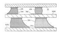
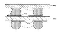
図1に示すように、第1の半導体パッケージ1aと第1のプリント配線板100aが複数のボール電極10aにより接続され、第2の半導体パッケージ1bと第2のプリント配線板100bが複数のボール電極10bにより接続される。第3のプリント配線板100cと第1のプリント配線板100aはボール電極20aを介して互に積層される。また、第1のプリント配線板100aと第2のプリント配線板100bはボール電極20bを介して互に積層される。 As shown in FIG. 1, the first semiconductor package 1a and the first printed
このような積層構造を備えた半導体装置において、ボール電極10aはプリント配線板100aに配置された電極パッド30aを介してプリント配線板100aに接続され、電極パッド30aはプリント配線板100aの面方向に凸部を有する。なお、本発明において面方向とは、プリント配線板の表面に沿った方向のことである。すなわち、電極パッド30aを、プリント配線板100aの表面に沿った平面で切断した場合の形状が、円形ではなく、円形の少なくとも一部に凸部を有している形状であることを意味している。ボール電極10bはプリント配線板100bに配置された電極パッド30bを介してプリント配線板100bに接続され、電極パッド30bはプリント配線板100bの面方向に凸部を有する。そして、電極パッド30a及び電極パッド30bを透視した透視陰影像が、各電極パッド30a、30bの前記凸部において少なくとも一部が重ならないように配置される。 In the semiconductor device having such a laminated structure, the
また、ボール電極20bはプリント配線板100aに配置された電極パッド50aを介してプリント配線板100aに接続され、電極パッド50aはプリント配線板100aの面方向に凸部を有する。そして、電極パッド30b及び電極パッド50aを透視した透視陰影像が、各電極パッド30b、50aの前記凸部において少なくとも一部が重ならないように配置される。 The
さらに、ボール電極10bは半導体パッケージ1bに配置された電極パッド40bを介して半導体パッケージ1bに接続され、電極パッド40bは半導体パッケージ1bの面方向に凸部を有する。そして、電極パッド30b及び電極パッド40bを透視した透視陰影像が、電極パッド30b及び電極パッド40bの前記凸部において少なくとも一部が重ならないように配置される。 Further, the
プリント配線板100aのボール電極20bが配置される表面側に対して反対側の裏面側のボール電極20aは、プリント配線板100aに配置された電極パッド60aを介してプリント配線板100aに接続される。電極パッド60aはプリント配線板100aの面方向に凸部を有する。そして、電極パッド50a及び電極パッド60aを透視した透視陰影像が、電極パッド50a及び電極パッド60aの前記凸部において少なくとも一部が重ならないように配置される。 The
電極パッド30a、30b、40a、40bは同径及び同軸である。また、電極パッド50a、60aも同径及び同軸である。 The
このように、ボール電極10aを介して半導体パッケージ1aはプリント配線板100aに実装され、ボール電極10bを介して半導体パッケージ1bはプリント配線板100bに実装される。また、ボール電極20bによりプリント配線板100a、100bが互に接続され、ボール電極20aによりプリント配線板100aとプリント配線板100cが接続される。 Thus, the semiconductor package 1a is mounted on the printed
そして、ボール電極10aとその直下に位置するボール電極10bは同外径(同径)で同じ中心軸(同軸)を有する。ボール電極20aとその直下に位置するボール電極20bは同外径(同径)で同じ中心軸(同軸)を有する。 The
図2は、図1の半導体装置の一部であるボール電極10bと、その直下に位置するボール電極10aを含む領域を示す断面図である。 FIG. 2 is a cross-sectional view showing a region including the
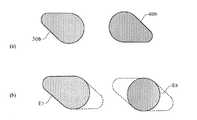
図3の(a)は、図2におけるボール電極10aが接続される電極パッド30aのプリント配線板100aの面方向の平面形状と、ボール電極10bが接続される電極パッド30bのプリント配線板100bの面方向の平面形状を示している。また、図3の(b)は、図2に示すボール電極10b及びボール電極10aを透視した陰影像(透視陰影像)を示している。 FIG. 3A shows a planar shape of the printed
図2の左側のボール電極10bは、電極パッド30bの凸部に充分に拡がった状態で電極パッド30bに接合している。また、ボール電極10aは電極パッド30aの凸部には拡がっていない状態で電極パッド30aに接合している。陰影像E1は、このときのボール電極10a及びボール電極10bを透視したものである。図2の右側のボール電極10bは、電極パッド30bの凸部には拡がっていない状態で電極パッド30bに接合している。また、ボール電極10aは電極パッド30aの凸部には拡がっていない状態で電極パッド30aに接合している。陰影像E2は、このときのボール電極10a及びボール電極10bを透視したものである。 The
図3の(a)に示すように、ボール電極10aが接続される電極パッド30aと、ボール電極10bが接続される電極パッド30bの形状を、円形に凸部が付加されたティアードロップ(涙粒)形状としている。このため、陰影像E1、E2の形状の違いをX線検査装置で判定することによって、ボール電極10aの電極パッド30aに対する接合状態と、ボール電極10bの電極パッド30bに対する接合状態を容易に検出できる。 As shown in FIG. 3 (a), the shape of the
接合状態の良否判定は、たとえば、陰影像(E1、E2)の真円度が、電極パッド(30a、30b)に接合する前のボール電極(10a、10b)の外径の30%以上であるときを良品、30%未満であるときを不良とすることができる。ただし、この良否判定の基準は、使用するボール電極の材質や、半導体装置の使用目的により設定することができる。 The determination of the quality of the bonded state is, for example, that the roundness of the shadow image (E1, E2) is 30% or more of the outer diameter of the ball electrode (10a, 10b) before being bonded to the electrode pad (30a, 30b). A time can be regarded as a non-defective product and less than 30% as a defective product. However, the criteria for the quality determination can be set according to the material of the ball electrode used and the purpose of use of the semiconductor device.
図4は、ボール電極10bと、その直下に位置するボール電極20bを含む領域を示す断面図である。 FIG. 4 is a cross-sectional view showing a region including the
図5の(a)は、図4におけるボール電極10aが接続される電極パッド30aのプリント配線板100aの面方向の平面形状と、ボール電極10bが接続される電極パッド30bのプリント配線板100bの面方向の平面形状を示している。また、図5の(b)は、ボール電極10b及びボール電極20bを透視した陰影像(透視陰影像)を示している。 5A shows the planar shape of the printed
図4の左側のボール電極10bは、電極パッド30bの凸部に充分に拡がった状態で電極パッド30bに接合している。また、ボール電極20bは、電極パッド50aに充分に拡がった状態での凸部を含んで電極パッド50aに接合している。陰影像E3は、このときのボール電極10b及びボール電極20bを透視したものである。図4の右側のボール電極10bは、電極パッド30bの凸部には拡がっていない状態で電極パッド30bに接合している。また、ボール電極20bは電極パッド50aに充分に拡がった状態で電極パッド50aに接合している。陰影像E4は、このときのボール電極10b及びボール電極20bを透視したものである。 The
ボール電極10bが接続される電極パッド30bと、ボール電極20bが接続される電極パッド50bの形状を、円形に凸部が付加されたティアードロップ(涙粒)形状としている。このため、陰影像E3と陰影像E4の形状の違いをX線検査装置で判定することによって、ボール電極10bの電極パッド30bに対する接合状態と、ボール電極20bの電極パッド50aに対する接合状態を容易に検出できる。 The shape of the
図6は、ボール電極20bと、その直下に位置するボール電極20aを含む領域を示す断面図である。 FIG. 6 is a cross-sectional view showing a region including the
図7の(a)は、図6におけるボール電極20bが接続される電極パッド50aのプリント配線板100aの面方向の平面形状と、ボール電極20aが接続される電極パッド60aのプリント配線板100aの面方向の平面形状を示している。また、図7の(b)は、ボール電極20b及びボール電極20aを透視した陰影像(透視陰影像)を示している。 FIG. 7A shows a planar shape of the printed
図6の左側のボール電極20bは、電極パッド50bの凸部に充分に拡がった状態で電極パッド50bに接合している。また、ボール電極20aは、電極パッド60aの凸部には拡がっていない状態で電極パッド60aに接合している。陰影像E5は、このときのボール電極20b及びボール電極20aを透視した陰影像である。図6の右側のボール電極20bは、電極パッド50bの凸部には拡がっていない状態で電極パッド50aに接合している。また、ボール電極20aは、電極パッド60aの凸部には拡がっていない状態で電極パッド60aに接合している。陰影像E6は、このときのボール電極20b及びボール電極20aを透視したものである。 The
ボール電極20bが接続される電極パッド50aと、ボール電極20aが接続される電極パッド60aの形状を、円形に凸部が付加されたティアードロップ(涙粒)形状としている。このため、陰影像E5と陰影像E6の形状の違いをX線検査装置で判定することによって、ボール電極20bの電極パッド50aに対する接合状態と、ボール電極20aの電極パッド60aに対する接合状態を容易に検出できる。 The shape of the
図8は、プリント配線板100bに半導体パッケージ1bを実装した実装構造におけるボール電極10bを含む領域の断面図である。 FIG. 8 is a cross-sectional view of a region including the
図9の(a)は、図8におけるボール電極10bの上部が接続される電極パッド40bのプリント配線板1bの面方向の平面形状と、ボール電極10bの下部が接続される電極パッド30bのプリント配線板100bの面方向の平面形状を示している。図9の(b)は、ボール電極10bを透視した陰影像(透視陰影像)を示している。 FIG. 9A shows a planar shape of the printed
図8の左側のボール電極10bは、電極パッド40bの凸部には拡がっていない状態で電極パッド40bに接合している。また、ボール電極10bは、電極パッド30bの凸部に充分に拡がった状態で電極パッド30bに接合している。陰影像E7は、このときのボール電極10bを透視したものである。図8の右側のボール電極10bは、電極パッド40bの凸部には拡がっていない状態で電極パッド40bに接合している。また、ボール電極10bは、電極パッド30bの凸部には拡がっていない状態で電極パッド30bに接合している。陰影像E6は、このときのボール電極10bを透視したものである。 The
ボール電極10bが接続される電極パッド30b及び電極パッド40bの形状を、円形に凸部が付加されたティアードロップ(涙粒)形状としている。このため、陰影像E7及び陰影像E8の形状の違いをX線検査装置で判定することによって、ボール電極10bの電極パッド30b、40bに対する接合状態を容易に検出できる。 The shape of the
各電極パッドの形状は、ティアードロップ形状に限らず、例えば図10に示すように、円に十字状に突起を設けた形状S1、S2、平行四辺形状S3、S4、円に五角形状に突起を設けた形状S5、S6、円に三角形状に突起を設けた形状S7、S8でもよい。 The shape of each electrode pad is not limited to the teardrop shape. For example, as shown in FIG. 10, the shapes S1 and S2, the parallelograms S3 and S4 provided with protrusions in a cross shape on the circle, and the pentagonal protrusions on the circle. The provided shapes S5 and S6, and the shapes S7 and S8 in which protrusions are provided in a triangular shape on the circle may be used.
1a 第1の半導体パッケージ
1b 第2の半導体パッケージ
10a、10b、20a、20b ボール電極
30a、30b、40a、40b、50a、60a 電極パッド
100a 第1のプリント配線板
100b 第2のプリント配線板
100c 第3のプリント配線板DESCRIPTION OF SYMBOLS 1a
Claims (3)
Translated fromJapanese前記電極パッドは、第1層及び第2層にそれぞれ配設された一対の電極パッドの透視陰影像が、互いに一部が重なると共に、これらの透視陰影像の非重なり部分の少なくとも一部が、他の全ての電極パッドの透視陰影像と重ならないように配設され、
上部ボール電極及び下部ボール電極はそれぞれ、互いの透視陰影像が重なり合う形で前記第1層及び第2層の前記一対の電極パッドに接合された、
ことを特徴とする半導体装置。In a semiconductor device having a laminated structure in which a plurality of printed wiring boards are laminated to each other via three or more ball electrodes joined to electrode pads of the printed wiring board,
In the electrode pad, the perspective shadow images of the pair of electrode pads respectively disposed in the first layer and the second layer partially overlap each other, and at least a part of the non-overlapping portions of these perspective shadow images is Arranged so as not to overlap the fluoroscopic shadow image of all other electrode pads,
Each of the upper ball electrode and the lower ball electrode is bonded to the pair of electrode pads of the first layer and the second layer in such a manner that the perspective shadow images overlap each other.
A semiconductor device.
請求項1記載の半導体装置。Each of the pair of electrode pads of the first layer and the second layer includes a convex portion formed so that a part thereof deviates from the overlapping portion.
The semiconductor device according to claim 1 .
請求項1記載の半導体装置。Each of the pair of electrode pads of the first layer and the second layer partially overlaps with all other electrode pads in which a perspective shadow image is disposed at a position corresponding to the pair of electrode pads of the other layer. Formed as
The semiconductor device according to claim 1 .
Priority Applications (6)
| Application Number | Priority Date | Filing Date | Title |
|---|---|---|---|
| JP2007134927AJP5207659B2 (en) | 2007-05-22 | 2007-05-22 | Semiconductor device |
| PCT/JP2008/059754WO2008143359A1 (en) | 2007-05-22 | 2008-05-21 | Electronic circuit device |
| CN2008800131157ACN101663925B (en) | 2007-05-22 | 2008-05-21 | Electronic circuit device |
| US12/530,708US7906733B2 (en) | 2007-05-22 | 2008-05-21 | Electronic circuit device |
| EP08764770AEP2153706A4 (en) | 2007-05-22 | 2008-05-21 | Electronic circuit device |
| KR1020097026037AKR101065877B1 (en) | 2007-05-22 | 2008-05-21 | Electronic circuit devices |
Applications Claiming Priority (1)
| Application Number | Priority Date | Filing Date | Title |
|---|---|---|---|
| JP2007134927AJP5207659B2 (en) | 2007-05-22 | 2007-05-22 | Semiconductor device |
Publications (3)
| Publication Number | Publication Date |
|---|---|
| JP2008294014A JP2008294014A (en) | 2008-12-04 |
| JP2008294014A5 JP2008294014A5 (en) | 2010-07-08 |
| JP5207659B2true JP5207659B2 (en) | 2013-06-12 |
Family
ID=40032037
Family Applications (1)
| Application Number | Title | Priority Date | Filing Date |
|---|---|---|---|
| JP2007134927AExpired - Fee RelatedJP5207659B2 (en) | 2007-05-22 | 2007-05-22 | Semiconductor device |
Country Status (6)
| Country | Link |
|---|---|
| US (1) | US7906733B2 (en) |
| EP (1) | EP2153706A4 (en) |
| JP (1) | JP5207659B2 (en) |
| KR (1) | KR101065877B1 (en) |
| CN (1) | CN101663925B (en) |
| WO (1) | WO2008143359A1 (en) |
Families Citing this family (15)
| Publication number | Priority date | Publication date | Assignee | Title |
|---|---|---|---|---|
| JP5191927B2 (en)* | 2009-02-26 | 2013-05-08 | アルプス電気株式会社 | MEMS sensor and manufacturing method thereof |
| US8716868B2 (en) | 2009-05-20 | 2014-05-06 | Panasonic Corporation | Semiconductor module for stacking and stacked semiconductor module |
| KR101671258B1 (en)* | 2009-05-20 | 2016-11-01 | 파나소닉 아이피 매니지먼트 가부시키가이샤 | Stacked semiconductor module |
| JP2011124382A (en)* | 2009-12-10 | 2011-06-23 | Fujitsu Ltd | Printed wiring board, printed wiring board unit, and electronic device |
| JP5143211B2 (en) | 2009-12-28 | 2013-02-13 | パナソニック株式会社 | Semiconductor module |
| JP6091053B2 (en)* | 2011-09-14 | 2017-03-08 | キヤノン株式会社 | Semiconductor device, printed circuit board and electronic product |
| US9001522B2 (en)* | 2011-11-15 | 2015-04-07 | Apple Inc. | Printed circuits with staggered contact pads and compact component mounting arrangements |
| US8810020B2 (en)* | 2012-06-22 | 2014-08-19 | Freescale Semiconductor, Inc. | Semiconductor device with redistributed contacts |
| WO2015151292A1 (en)* | 2014-04-04 | 2015-10-08 | 三菱電機株式会社 | Printed wire board unit |
| JP6230520B2 (en)* | 2014-10-29 | 2017-11-15 | キヤノン株式会社 | Printed circuit board and electronic device |
| JP6772232B2 (en)* | 2018-10-03 | 2020-10-21 | キヤノン株式会社 | Printed circuit boards and electronic devices |
| WO2021083032A1 (en)* | 2019-10-28 | 2021-05-06 | 天芯互联科技有限公司 | Packaging structure and manufacturing method therefor |
| CN110849918B (en)* | 2019-10-31 | 2021-11-09 | 北京时代民芯科技有限公司 | Nondestructive detection method and system for welding spot defects of flip chip bonding device |
| JP7155214B2 (en)* | 2020-09-28 | 2022-10-18 | キヤノン株式会社 | Printed circuit boards and electronics |
| TW202437821A (en)* | 2023-03-08 | 2024-09-16 | 群創光電股份有限公司 | Electronic device |
Family Cites Families (49)
| Publication number | Priority date | Publication date | Assignee | Title |
|---|---|---|---|---|
| DK291184D0 (en)* | 1984-06-13 | 1984-06-13 | Boeegh Petersen Allan | METHOD AND DEVICE FOR TESTING CIRCUIT PLATES |
| US5086337A (en)* | 1987-01-19 | 1992-02-04 | Hitachi, Ltd. | Connecting structure of electronic part and electronic device using the structure |
| US5012502A (en)* | 1990-06-18 | 1991-04-30 | Irt Corporation | Method for determining degree of interconnection of solder joints using X-ray inspection |
| US5811982A (en)* | 1995-11-27 | 1998-09-22 | International Business Machines Corporation | High density cantilevered probe for electronic devices |
| JP2710544B2 (en)* | 1993-09-30 | 1998-02-10 | インターナショナル・ビジネス・マシーンズ・コーポレイション | Probe structure, method of forming probe structure |
| CA2113752C (en)* | 1994-01-19 | 1999-03-02 | Stephen Michael Rooks | Inspection system for cross-sectional imaging |
| US5400220A (en)* | 1994-05-18 | 1995-03-21 | Dell Usa, L.P. | Mechanical printed circuit board and ball grid array interconnect apparatus |
| US5802699A (en)* | 1994-06-07 | 1998-09-08 | Tessera, Inc. | Methods of assembling microelectronic assembly with socket for engaging bump leads |
| US5477933A (en)* | 1994-10-24 | 1995-12-26 | At&T Corp. | Electronic device interconnection techniques |
| JPH08236586A (en)* | 1994-12-29 | 1996-09-13 | Nitto Denko Corp | Semiconductor device and manufacturing method thereof |
| JPH0951017A (en)* | 1995-08-04 | 1997-02-18 | Fujitsu Ltd | Semiconductor module |
| KR0182073B1 (en)* | 1995-12-22 | 1999-03-20 | 황인길 | Semiconductor chip scale semiconductor package and manufacturing method thereof |
| JPH09214088A (en) | 1996-01-31 | 1997-08-15 | Sumitomo Kinzoku Electro Device:Kk | Mounting structure of ceramic board to printed board |
| JPH09219583A (en) | 1996-02-09 | 1997-08-19 | Hitachi Ltd | Solder bump connection method |
| US6880245B2 (en)* | 1996-03-12 | 2005-04-19 | International Business Machines Corporation | Method for fabricating a structure for making contact with an IC device |
| US6086386A (en)* | 1996-05-24 | 2000-07-11 | Tessera, Inc. | Flexible connectors for microelectronic elements |
| US5953816A (en)* | 1997-07-16 | 1999-09-21 | General Dynamics Information Systems, Inc. | Process of making interposers for land grip arrays |
| JPH1154884A (en)* | 1997-08-06 | 1999-02-26 | Nec Corp | Mounting structure for semiconductor device |
| JPH11233936A (en)* | 1998-02-18 | 1999-08-27 | Hitachi Shonan Denshi Co Ltd | Solder joint inspection method and surface mount wiring board using the method |
| US6451624B1 (en)* | 1998-06-05 | 2002-09-17 | Micron Technology, Inc. | Stackable semiconductor package having conductive layer and insulating layers and method of fabrication |
| US6050832A (en)* | 1998-08-07 | 2000-04-18 | Fujitsu Limited | Chip and board stress relief interposer |
| USRE41515E1 (en)* | 1998-08-12 | 2010-08-17 | Tokyo Electron Limited | Contactor and production method for contactor |
| DE19839760A1 (en)* | 1998-09-01 | 2000-03-02 | Bosch Gmbh Robert | Method for connecting electronic components to a carrier substrate and method for checking such a connection |
| JP2001068836A (en)* | 1999-08-27 | 2001-03-16 | Mitsubishi Electric Corp | Printed wiring board, semiconductor module, and method of manufacturing semiconductor module |
| US6380060B1 (en)* | 2000-03-08 | 2002-04-30 | Tessera, Inc. | Off-center solder ball attach and methods therefor |
| US6333563B1 (en)* | 2000-06-06 | 2001-12-25 | International Business Machines Corporation | Electrical interconnection package and method thereof |
| US6507118B1 (en)* | 2000-07-14 | 2003-01-14 | 3M Innovative Properties Company | Multi-metal layer circuit |
| US6414248B1 (en)* | 2000-10-04 | 2002-07-02 | Honeywell International Inc. | Compliant attachment interface |
| US6680212B2 (en)* | 2000-12-22 | 2004-01-20 | Lucent Technologies Inc | Method of testing and constructing monolithic multi-chip modules |
| US6889429B2 (en)* | 2001-03-26 | 2005-05-10 | Semiconductor Components Industries, L.L.C. | Method of making a lead-free integrated circuit package |
| JP4191908B2 (en) | 2001-04-18 | 2008-12-03 | 株式会社東芝 | Multilayer semiconductor device |
| US6509530B2 (en)* | 2001-06-22 | 2003-01-21 | Intel Corporation | Via intersect pad for electronic components and methods of manufacture |
| US6657134B2 (en)* | 2001-11-30 | 2003-12-02 | Honeywell International Inc. | Stacked ball grid array |
| JP3601714B2 (en) | 2002-01-11 | 2004-12-15 | 富士通株式会社 | Semiconductor device and wiring board |
| JP2003218505A (en) | 2002-01-17 | 2003-07-31 | Matsushita Electric Ind Co Ltd | Printed circuit board, printed circuit board unit, method of inspecting and manufacturing printed circuit board unit, and communication device using printed circuit board unit |
| KR100864916B1 (en)* | 2002-05-23 | 2008-10-22 | 캐스케이드 마이크로테크 인코포레이티드 | Probes for Testing Devices Under Test |
| US6703851B1 (en)* | 2002-08-05 | 2004-03-09 | Exatron, Inc. | Test socket interposer |
| JP3951966B2 (en)* | 2003-05-30 | 2007-08-01 | セイコーエプソン株式会社 | Semiconductor device |
| US7317165B2 (en)* | 2003-06-24 | 2008-01-08 | Ngk Spark Plug Co., Ltd. | Intermediate substrate, intermediate substrate with semiconductor element, substrate with intermediate substrate, and structure having semiconductor element, intermediate substrate and substrate |
| US7566960B1 (en)* | 2003-10-31 | 2009-07-28 | Xilinx, Inc. | Interposing structure |
| US7176043B2 (en)* | 2003-12-30 | 2007-02-13 | Tessera, Inc. | Microelectronic packages and methods therefor |
| DE602004016483D1 (en)* | 2004-07-16 | 2008-10-23 | St Microelectronics Sa | Electronic circuit arrangement, apparatus with such an arrangement and manufacturing method |
| US7105918B2 (en)* | 2004-07-29 | 2006-09-12 | Micron Technology, Inc. | Interposer with flexible solder pad elements and methods of manufacturing the same |
| US7317249B2 (en)* | 2004-12-23 | 2008-01-08 | Tessera, Inc. | Microelectronic package having stacked semiconductor devices and a process for its fabrication |
| US7462939B2 (en)* | 2005-10-20 | 2008-12-09 | Honeywell International Inc. | Interposer for compliant interfacial coupling |
| TW200737506A (en)* | 2006-03-07 | 2007-10-01 | Sanyo Electric Co | Semiconductor device and manufacturing method of the same |
| US7687391B2 (en)* | 2006-09-27 | 2010-03-30 | International Business Machines Corporation | Electrically optimized and structurally protected via structure for high speed signals |
| US7719121B2 (en)* | 2006-10-17 | 2010-05-18 | Tessera, Inc. | Microelectronic packages and methods therefor |
| US20080093749A1 (en)* | 2006-10-20 | 2008-04-24 | Texas Instruments Incorporated | Partial Solder Mask Defined Pad Design |
- 2007
- 2007-05-22JPJP2007134927Apatent/JP5207659B2/ennot_activeExpired - Fee Related
- 2008
- 2008-05-21CNCN2008800131157Apatent/CN101663925B/ennot_activeExpired - Fee Related
- 2008-05-21WOPCT/JP2008/059754patent/WO2008143359A1/enactiveApplication Filing
- 2008-05-21USUS12/530,708patent/US7906733B2/ennot_activeExpired - Fee Related
- 2008-05-21KRKR1020097026037Apatent/KR101065877B1/ennot_activeExpired - Fee Related
- 2008-05-21EPEP08764770Apatent/EP2153706A4/ennot_activeWithdrawn
Also Published As
| Publication number | Publication date |
|---|---|
| CN101663925A (en) | 2010-03-03 |
| EP2153706A1 (en) | 2010-02-17 |
| US7906733B2 (en) | 2011-03-15 |
| CN101663925B (en) | 2011-11-16 |
| EP2153706A4 (en) | 2013-01-23 |
| WO2008143359A1 (en) | 2008-11-27 |
| US20100084177A1 (en) | 2010-04-08 |
| KR20100007998A (en) | 2010-01-22 |
| JP2008294014A (en) | 2008-12-04 |
| KR101065877B1 (en) | 2011-09-19 |
Similar Documents
| Publication | Publication Date | Title |
|---|---|---|
| JP5207659B2 (en) | Semiconductor device | |
| US20090114436A1 (en) | Substrate structure | |
| CN109095434B (en) | Sensor structure and its manufacturing method | |
| JP5528273B2 (en) | Wiring circuit board, wiring circuit board assembly sheet, and method for manufacturing the same | |
| US9729124B2 (en) | Piezoelectric vibration component having distinguishable opposing principal surfaces | |
| JP2008147472A (en) | Semiconductor device and manufacturing method therefor | |
| CN106852009B (en) | Suspension board with circuit and method for manufacturing suspension board with circuit | |
| JPH08264712A (en) | Semiconductor device | |
| JP2008164427A (en) | Probe unit board | |
| JP2008227429A (en) | Electronic circuit module and multilayer wiring board | |
| US9972567B2 (en) | Multilayer substrate, component mounted board, and method for producing component mounted board | |
| JP2004214699A (en) | Semiconductor mounting circuit board and semiconductor device having the same | |
| JPS6151510A (en) | Inspecting method for interlayer deviation of multilayer printed board | |
| KR100652440B1 (en) | Semiconductor package, stack package using the package, and method of forming the stack package | |
| KR102667735B1 (en) | flexible LED display module and LED display panel comprising the same | |
| JPWO2017212964A1 (en) | PCB connection structure | |
| JP5546363B2 (en) | Semiconductor device and manufacturing method of semiconductor device | |
| JP2007266078A (en) | Semiconductor device, semiconductor device having chip-on-chip structure, and method for manufacturing semiconductor device | |
| JPWO2004093191A1 (en) | Semiconductor device | |
| JP5868281B2 (en) | Wiring board | |
| JP4151565B2 (en) | Tape carrier | |
| US9870525B2 (en) | Semiconductor laser element and method of obtaining information from the semiconductor laser element | |
| JP4800881B2 (en) | Manufacturing method of multilayer printed wiring board | |
| JP2008021859A (en) | Printed wiring board | |
| JP2728569B2 (en) | Distributed tactile sensor |
Legal Events
| Date | Code | Title | Description |
|---|---|---|---|
| RD03 | Notification of appointment of power of attorney | Free format text:JAPANESE INTERMEDIATE CODE: A7423 Effective date:20090527 | |
| A521 | Request for written amendment filed | Free format text:JAPANESE INTERMEDIATE CODE: A523 Effective date:20100524 | |
| A621 | Written request for application examination | Free format text:JAPANESE INTERMEDIATE CODE: A621 Effective date:20100524 | |
| RD03 | Notification of appointment of power of attorney | Free format text:JAPANESE INTERMEDIATE CODE: A7423 Effective date:20120203 | |
| A131 | Notification of reasons for refusal | Free format text:JAPANESE INTERMEDIATE CODE: A131 Effective date:20121023 | |
| A521 | Request for written amendment filed | Free format text:JAPANESE INTERMEDIATE CODE: A523 Effective date:20121225 | |
| TRDD | Decision of grant or rejection written | ||
| A01 | Written decision to grant a patent or to grant a registration (utility model) | Free format text:JAPANESE INTERMEDIATE CODE: A01 Effective date:20130122 | |
| A61 | First payment of annual fees (during grant procedure) | Free format text:JAPANESE INTERMEDIATE CODE: A61 Effective date:20130219 | |
| FPAY | Renewal fee payment (event date is renewal date of database) | Free format text:PAYMENT UNTIL: 20160301 Year of fee payment:3 | |
| R151 | Written notification of patent or utility model registration | Ref document number:5207659 Country of ref document:JP Free format text:JAPANESE INTERMEDIATE CODE: R151 | |
| FPAY | Renewal fee payment (event date is renewal date of database) | Free format text:PAYMENT UNTIL: 20160301 Year of fee payment:3 | |
| LAPS | Cancellation because of no payment of annual fees |