JP5204941B2 - Toroidal plasma chamber excited from outside - Google Patents
Toroidal plasma chamber excited from outsideDownload PDFInfo
- Publication number
- JP5204941B2 JP5204941B2JP2002519385AJP2002519385AJP5204941B2JP 5204941 B2JP5204941 B2JP 5204941B2JP 2002519385 AJP2002519385 AJP 2002519385AJP 2002519385 AJP2002519385 AJP 2002519385AJP 5204941 B2JP5204941 B2JP 5204941B2
- Authority
- JP
- Japan
- Prior art keywords
- plasma
- conduit
- wafer
- plasma chamber
- chamber
- Prior art date
- Legal status (The legal status is an assumption and is not a legal conclusion. Google has not performed a legal analysis and makes no representation as to the accuracy of the status listed.)
- Expired - Lifetime
Links
Images


Classifications
- H—ELECTRICITY
- H01—ELECTRIC ELEMENTS
- H01J—ELECTRIC DISCHARGE TUBES OR DISCHARGE LAMPS
- H01J37/00—Discharge tubes with provision for introducing objects or material to be exposed to the discharge, e.g. for the purpose of examination or processing thereof
- H01J37/32—Gas-filled discharge tubes
- H01J37/32009—Arrangements for generation of plasma specially adapted for examination or treatment of objects, e.g. plasma sources
- H01J37/32082—Radio frequency generated discharge
- H01J37/321—Radio frequency generated discharge the radio frequency energy being inductively coupled to the plasma
- H—ELECTRICITY
- H01—ELECTRIC ELEMENTS
- H01J—ELECTRIC DISCHARGE TUBES OR DISCHARGE LAMPS
- H01J37/00—Discharge tubes with provision for introducing objects or material to be exposed to the discharge, e.g. for the purpose of examination or processing thereof
- H01J37/32—Gas-filled discharge tubes
- H01J37/32009—Arrangements for generation of plasma specially adapted for examination or treatment of objects, e.g. plasma sources
- H01J37/32082—Radio frequency generated discharge
- H—ELECTRICITY
- H01—ELECTRIC ELEMENTS
- H01J—ELECTRIC DISCHARGE TUBES OR DISCHARGE LAMPS
- H01J37/00—Discharge tubes with provision for introducing objects or material to be exposed to the discharge, e.g. for the purpose of examination or processing thereof
- H01J37/32—Gas-filled discharge tubes
- H01J37/32431—Constructional details of the reactor
- H01J37/3244—Gas supply means
Landscapes
- Physics & Mathematics (AREA)
- Engineering & Computer Science (AREA)
- Plasma & Fusion (AREA)
- Chemical & Material Sciences (AREA)
- Analytical Chemistry (AREA)
- Plasma Technology (AREA)
- Drying Of Semiconductors (AREA)
- Physical Or Chemical Processes And Apparatus (AREA)
- Chemical Vapour Deposition (AREA)
Description
Translated fromJapanese (発明の属する技術分野)
本発明は、マイクロエレクトロニック回路、フラットパネルディスプレイ等の製造におけるワークピースの処理に用いられるプラズマリアクタ、及び特に、それらのためのプラズマ源に関する。(Technical field to which the invention belongs)
The present invention relates to plasma reactors used for processing workpieces in the manufacture of microelectronic circuits, flat panel displays and the like, and in particular to plasma sources therefor.
(技術の背景)
マイクロエレクトロニック回路においては、従来より増大する密度及び小さなフィーチャサイズに向かう傾向が続き、このようなデバイスのプラズマ処理をより困難にしている。例えば、コンタクトホールの直径は減少されるが、一方そのホールの深さは増大している。例えば、シリコンウエハ上の誘電体膜のプラズマ増強エッチング中に、ホトレジストに対する誘電体材料(例えば、二酸化シリコン)のエッチング選択性は、エッチングプロセスがコンタクトホールをエッチングするのに充分でなければならない。コンタクトホールの直径はホールを規定するホトレジストマスクを邪魔することなくその深さの10倍から15倍である。細かなホトリソグラフに対してより短い波長の光に向かう最近の傾向は薄いホトレジスト層を必要とし、その結果誘電体とホトレジストのエッチング選択性は、いままで以上に大きくなければならないので、この仕事(タスク)を非常に困難にする。この要求は、比較的遅いエッチング速度を有するプロセス、例えば容量性結合プラズマを用いる誘電体エッチングプロセスを使用することによって容易に受け入れられる。容量性結合プラズマのプラズマ密度は、誘導性結合プラズマの密度より比較的小さく、容量性結合プラズマのエッチングプロセスは、誘電体とホトレジストの良好なエッチング選択性を示す。容量性結合プロセスの問題点は、それが遅く、従って生産性が比較的小さいことである。このようなエッチングプロセスに生じる他の問題は、プラズマが一様に分布しないことである。(Technical background)
In microelectronic circuits, there is a continuing trend towards ever increasing density and small feature sizes, making plasma processing of such devices more difficult. For example, the diameter of the contact hole is reduced while the depth of the hole is increased. For example, during plasma enhanced etching of a dielectric film on a silicon wafer, the etch selectivity of the dielectric material (eg, silicon dioxide) to the photoresist must be sufficient for the etching process to etch the contact holes. The diameter of the contact hole is 10 to 15 times its depth without interfering with the photoresist mask that defines the hole. The recent trend toward shorter wavelength light for fine lithographs requires a thin photoresist layer, and as a result, the etch selectivity of the dielectric and photoresist must be greater than ever, so this work ( Task). This requirement is readily accommodated by using a process with a relatively slow etch rate, such as a dielectric etch process using a capacitively coupled plasma. The plasma density of the capacitively coupled plasma is relatively smaller than the density of the inductively coupled plasma, and the capacitively coupled plasma etching process exhibits good dielectric and photoresist etch selectivity. The problem with the capacitive coupling process is that it is slow and therefore the productivity is relatively small. Another problem that arises in such an etching process is that the plasma is not uniformly distributed.
生産性、即ちエッチング速度を増加するために、高密度プラズマが用いられている。一般に、高密度プラズマは誘導結合プラズマである。しかし、プロセスの先駆ガスは、フリーなフッ素、即ちホトレジストに対するエッチングの選択性を減少する種の高プラズマを形成して、高密度プラズマにおいて急速に分離する傾向にある。この傾向を減少するために、酸素を含有しない表面、例えばホトレジスト上に累積する傾向にあるフッ素含有エッチャント種及び1つまたはそれ以上のポリマー種において分離するフルオロカーボンプロセスガス、例えばCF2が用いられる。これはエッチング選択性を増加する傾向にある。酸素を含有する誘電体材料における酸素は、誘電体上にポリマーのピロリゼーションを増進し、その結果誘電体材料がエッチングされてポリマーが除去されるが、一方酸素含有材料(例えば、ホトレジスト)がポリマーによって覆われ続け、従ってエッチャントから保護される。問題は、より進んだデバイス設計を可能にするために、コンタクト開口の深さの増加とホトレジスト厚の減少によって、誘電体のエッチング中にホトレジストを傷つける可能性のある高密度プラズマプロセスが行われたことである。エッチング速度を増進するために、プラズマ密度が増加されるに従って、酸素を含まない材料、例えばホトレジストを保護するために多くのポリマーの豊富なプラズマが用いられなければならないので、酸素を含む誘電体の表面からのポリマー除去の速度は、特に小さな、制限された領域、例えば狭いコンタクト開口の底部においてかなり遅くなる。その結果、ホトレジストはかなり保護されるけれども、コンタクト開口がある深さに達すると、ポリマーの累積によって阻止されるために、エッチングプロセスに対してその可能性は増大される。一般に、エッチングの停止深さは、コンタクト開口の必要な深さより少ないのでデバイスは失敗する。コンタクト開口は、中間を絶縁する酸化シリコン層を介して上部のポリシリコン導体層と下部のポリシリコン導体層間に接続を与える。例えば、エッチングの停止深さが上部と下部のポリシリコン層間の距離より小さい場合、デバイスの失敗が生じる。代わりに、たとえば10:1または15:1のアスペクト比のコンタクト開口を有するデバイス設計のようなより進んだデバイス設計への実際のまたは信頼できる応用に対して狭くなりすぎるエッチング停止のない高密度プラズマを達成するためのプロセスウインドウの可能性が起きる。High density plasma is used to increase productivity, i.e., etch rate. Generally, high density plasma is inductively coupled plasma. However, the process precursor gas tends to form a high plasma of a species that reduces the selectivity of the etch to free fluorine, ie photoresist, and rapidly separates in the high density plasma. To reduce this tendency, a fluorocarbon process gas, such as CF2, is used that separates on fluorine-containing etchant species and one or more polymer species that tend to accumulate on oxygen-free surfaces, such as photoresist. This tends to increase etch selectivity. Oxygen in a dielectric material that contains oxygen enhances the pyrrolization of the polymer on the dielectric, which results in the dielectric material being etched away to remove the polymer, while the oxygen-containing material (eg, photoresist) is polymerized. Will continue to be covered by and thus protected from the etchant. The problem is that in order to allow for more advanced device design, increasing the contact opening depth and decreasing the photoresist thickness resulted in a high-density plasma process that could damage the photoresist during the dielectric etch. That is. In order to increase the etch rate, as the plasma density is increased, oxygen-free materials such as many polymer-rich plasmas must be used to protect the photoresist, so that oxygen-containing dielectrics The rate of polymer removal from the surface is considerably slower, especially in small, limited areas, such as the bottom of narrow contact openings. As a result, although the photoresist is well protected, its potential for the etching process is increased when the contact opening reaches a certain depth, because it is blocked by polymer accumulation. In general, the etch fails because the etch stop depth is less than the required depth of the contact opening. The contact opening provides a connection between the upper polysilicon conductor layer and the lower polysilicon conductor layer via a silicon oxide layer that insulates the middle. For example, device failure occurs when the etch stop depth is less than the distance between the upper and lower polysilicon layers. Instead, high density plasma without etch stop that becomes too narrow for actual or reliable application to more advanced device designs, such as device designs with contact openings of 10: 1 or 15: 1 aspect ratio, for example. The possibility of a process window to achieve
現在必要なものは、容量結合リアクタの選択性を有し、誘導結合のプラズマリアクタ(高密度プラズマを有する)のエッチング速度を有するリアクタである。単一のマシンリアクタにおいて両方の形式のリアクタの利点を実現することは困難であった。 What is currently needed is a reactor that has the selectivity of a capacitively coupled reactor and has the etching rate of an inductively coupled plasma reactor (with high density plasma). It has been difficult to realize the advantages of both types of reactors in a single machine reactor.
特に、ウエハまたはワークピースに面するオーバヘッドコイルアンテナを有する形式の高密度誘導結合プラズマリアクタのもつ1つの問題点は、エッチング速度を増大するために、コイルアンテナに供給される電力が増加されるに従って、電力がウエハの充分上方にあるプラズマ領域に吸収されるように、ウエハと天井のギャップが著しく大きくなければならないことである。これによって、強いRF磁界によるウエハ上のデバイス損傷のリスクを避けることができる。さらに、オーバヘッドコイルアンテナに供給されるRF電力の高レベルに対して、ウエハと天井のギャップを比較的大きくしなければならず、従って、小さなギャップの利点を実現することができない。 In particular, one problem with high density inductively coupled plasma reactors of the type having an overhead coil antenna facing the wafer or workpiece is that as the power supplied to the coil antenna is increased to increase the etch rate. The gap between the wafer and the ceiling must be significantly large so that power is absorbed by the plasma region well above the wafer. This avoids the risk of device damage on the wafer due to a strong RF magnetic field. In addition, for high levels of RF power supplied to the overhead coil antenna, the gap between the wafer and the ceiling must be relatively large, so the advantage of a small gap cannot be realized.
もし、天井が誘導結合リアクタのRF磁界に対して半導電性のウインドウであるか、または容量結合リアクタの導電性電極であるなら、ウエハと天井の小さなギャップの1つの利点は、天井が比較的小さなギャップ距離(例えば、1または2インチオーダー)にあるウエハの面を横切って与えることができる増大された電位または接地基準である。 If the ceiling is a semiconductive window with respect to the RF field of the inductively coupled reactor or the conductive electrode of the capacitively coupled reactor, one advantage of the small gap between the wafer and the ceiling is that the ceiling is relatively An increased potential or ground reference that can be applied across the surface of a wafer at a small gap distance (eg, on the order of 1 or 2 inches).
したがって、誘導結合リアクタのイオン密度とエッチング速度を有する容量結合リアクタの選択性をもつだけでなく、更に、基本的な制限、例えばプラズマシースの厚さ以外のウエハと天井のギャップ長に関する従来の制限をもたないリアクタを得ることが必要である。さらに、供給されたRFプラズマソース電力を必ずしも増加することなくイオン密度とエッチング速度が増大される容量結合リアクタの選択性と誘導結合リアクタのエッチング速度を有するリアクタを得ることが必要である。 Thus, in addition to the selectivity of capacitively coupled reactors with ion density and etch rate of inductively coupled reactors, there are also basic limitations such as conventional limitations on wafer-to-ceiling gap length other than plasma sheath thickness. It is necessary to obtain a reactor without Furthermore, it is necessary to obtain a reactor having the selectivity of a capacitively coupled reactor and the etching rate of an inductively coupled reactor in which the ion density and etch rate are increased without necessarily increasing the supplied RF plasma source power.
(本発明の概要)
ワークピースを処理するためのプラズマリアクタは、エンクロージャを有し、このエンクロージャ内のワークピース支持体は、エンクロージャの上方にある部分に面しており、このワークピース支持体とエンクロージャの上方にある部分はワークピース支持体の直径を横切って広がる、それらの間にプロセス領域を画定する。このエンクロージャは、ワークピース支持体のほぼ反対側の近くにそれらを介して少なくとも第1と第2の開口を有する。プロセス領域の外側にある少なくとも1つの中空導管が第1と第2の開口に接続され、導管を通して延び、プロセス領域を横切る第1のトロイダルパス(通路)を与える。RF電力を受けるのに適合された第1のコイルアンテナが中空導管の内部に誘導的に結合され、トロイダルパスにプラズマを維持することができる。(Outline of the present invention)
A plasma reactor for processing a workpiece has an enclosure, and a workpiece support in the enclosure faces a portion above the enclosure, the workpiece support and a portion above the enclosure. Defines a process area between them that extends across the diameter of the workpiece support. The enclosure has at least first and second apertures therethrough substantially near the opposite side of the workpiece support. At least one hollow conduit outside the process region is connected to the first and second openings and extends through the conduit to provide a first toroidal path (passage) across the process region. A first coil antenna adapted to receive RF power is inductively coupled inside the hollow conduit to maintain a plasma in the toroidal path.
(好適な実施の形態の詳細な説明)
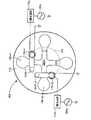
プラズマリアクタチャンバの概要
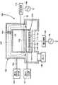
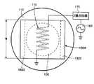
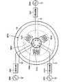
図1を参照すると、円筒上の側壁105と天井110によって囲まれたプラズマリアクタチャンバ100が半導体ウエハまたはワークピース120を支持するためのウエハペデスタルを有している。プロセスガス源125が側壁105を通して延びるガス入口ノズル130A−130Dを介してプロセスガスをチャンバ100へ供給する。真空ポンプ135がチャンバ100内の圧力を制御し、圧力を一般に0.5ミリトル(mT)以下に保つ。半分のトロイダル中空チューブのエンクロージャまたは導管(コンジット)150が半円形状に天井の上に延びている。導管150は、天井110から外側外方に延びているけれども、それにも拘わらずリアクタの一部であり、チャンバの壁を形成している。内部的には、それはリアクタの他の場所に存在している同じ排気された雰囲気を共有している。実際に、真空ポンプ135は、図1に示されたチャンバの主な部分の底部に結合される代わりに、これは好適ではないけれども導管150に結合されてもよい。導管150は、リアクタの天井110における第1の開口155の周りにシールされた1つの開口端150aとリアクタの天井110における第2の開口160の周りにシールされた他の開口端150bを有する。2つの開口またはポート150、160は、ウエハ支持ペデスタル115のほぼ反対側に配置されている。中空の導管150は、それが1つの開口においてチャンバの主な部分を出て、他の開口で再び入る流路を提供している点で、リエントラントである。この明細書において、導管は中空であり、プラズマが流れることができる閉じたパスの一部を与えることおいて、導管150は半分のドロイダルとして記載されており、全体の通路はウエハ支持ペデスタル115の上にある全体のプロセス領域を横切って流れることによって完成される。用語”Atorroidal”@の使用にもかかわらず、通路の軌道ばかりでなく通路または導管150の断面形状も円形または非円形、正方形、矩形または他のあらゆる形状、即ち規則的な形状または不規則な形状であることができる。(Detailed description of preferred embodiments)
Plasma Reactor Chamber Overview Referring to FIG. 1, a
外部の導管150は比較的薄い導体、例えばシート状の金属から形成されることができるが、チャンバ内の圧力に耐えるために充分な強度を有している。中空導管150のシート金属における渦電流を抑制するために(及びそれによって、導管150の内部へのRF誘導性磁界の結合を容易にする)、導管を2つの環状区分に分けるように、絶縁ギャップ152が中空の導管150を横切って、及び導管を介して伸びている。ギャップ152は絶縁性材料、例えばシート金属スキンに代えてセラミックのリング154によって満たされているので、ギャップは真空気密である。第2の絶縁ギャップ153が設けられており、その結果導管150の1つの区分は電気的に浮いている。バイアスRF発生器162がインピーダンス整合回路(図面では、Z整合回路として示す)164を介してウエハペデスタル115とウエハ120にRFバイアス電力を供給している。 The
代わりに、中空導管150は、導電性シートの金属の代わりに非導電性材料から形成されてもよい。非導電性材料は、例えばセラミックである。このような代替の実施の形態においては、ギャップ152または153は必要でない。 Alternatively, the
アンテナ、例えば中空導管150の一方の側に配置され、半分のトロイダルチューブの対称軸に平行な軸の周りに巻かれた巻線、即ちコイル165は、インピーダンス整合回路175を介してRF電源180に接続されている。アンテナ170は、更に、中空の導管150の反対側に配置され、第1の巻線165と同方向に巻かれた第2の巻線185を有しているので、両方の巻線からの磁界は有利に加わる。 An antenna, for example, a
チャンバ100からのプロセスガスは中空導管150を満たす。さらに、分離したプロセスガス源190がガス入口195を介して中空導管150ヘプロセスガスを直接供給する。外部の中空導管150におけるRF磁界は、チューブ内のガスをイオン化してプラズマを生成する。円形のコイルアンテナ170によって誘導されたRF磁界は、チューブ150内に形成されたプラズマがウエハ120と天井110間の領域を通して到達し、半分のトロイダル中空導管150を含むトロイダル通路を完成させるものである。ここで用いられているように、用語Atorroidal@は、この通路の閉じた、固定した性質を言うが、その断面形状または軌道には言及しないし、限定もしない。それらのいずれもは円形まはた非円形、または正方形又はその他の形状であってもよい。プラズマは、完全なトロイダル通路または閉じたプラズマ回路と考えられる領域を通して循環する。トロイダル領域は、ウエハ120の直径を横切って延び、ある実施の形態では、それが全体のウエハ表面を覆うようにウエハの面において充分な幅を有している。 Process gas from the
コイルアンテナ170からのRF誘導磁界はそれ自体閉じた磁界(全ての磁界である)を有し、従って、ここで説明される閉じたトロイダル通路をに沿ったプラズマ流を含む。RF誘導性磁界からの電力は、一般に閉じた通路に沿ったあらゆる位置で吸収され、その結果プラズマイオンは、一般に通路に沿って全て生成されると考えられている。RF電力の吸収及びプラズマイオンの生成速度は、多くのファクタに依存して閉じた通路に沿ったいろいろな位置の間で変わる。しかし、電流の密度は変わるけれども、電流は、一般に閉じた通路の長さに沿って一様である。この電流は、アンテナ170に供給されたRF信号の周波数で変化する。しかし、RF磁界によって誘導される電有は閉じているので、流れは閉じた通路の回路の周りに保全されなければならない。その結果閉じた通路のあらゆる部分に流れる電流量は、一般に通路の他の部分と同様である。以下に説明されるように、この事実は本発明において大きな利点として利用される。 The RF induced magnetic field from the
プラズマ流(プラズマカレント)が流れる閉じたトロイダル通路は、その通路を境にするいろいろな導電面に形成されるプラズマシースによって跳ね返される。これらの導電面は、中空導管150のシート金属、ウエハ(及び/又はウエハ支持ペデスタル)及びウエハの上方にある天井を含む。これらの導電面上に形成されるプラズマシースは、低質量の負の電子の大きな移動度及び重い質量の正の電子の小さな移動度のために電荷の不均衡の結果として生成される電荷空乏領域である。このようなプラズマシースは、このシースの下にある局部表面に垂直な電界を有する。従って、プロセス領域を通る、またはウエハの上にあるプロセスゾーンを通るRFプラズマ流は、ウエハに面する天井の面及びガス分配プレートに面するウエハの面に垂直な2つの電界の間によって制限され、その間を通過する。シースの厚さ(ワークピースまたは他の電極に与えられたRFバイアスを有する)は、電界が小さな領域、例えばウエハ上に集中される場合大きく、他の位置、例えば天井を覆うシースや大きな隣接するチャンバ壁の表面で小さい。従って、ウエハ上を覆うプラズマシースは非常に厚くなる。ウエハ及び天井のガス分配プレートシースの電界は互いにほぼ平行であり、プロセス領域のRFプラズマ流の流れの方向に垂直である。 A closed toroidal passage through which a plasma flow (plasma current) flows is rebounded by plasma sheaths formed on various conductive surfaces bordering on the passage. These conductive surfaces include the sheet metal of the
最初に、RF電力がコイルアンテナ170に加えられると、放電がギャップ152を横切って起き、中空導管150内のガスから容量結合されたプラズマを点弧する。その後、中空導管150を通るプラズマ流が増加するに従って、RF磁界の誘導結合がより支配的になるので、プラズマは誘導結合プラズマになる。代わりに、プラズマは他の手段、例えばワークピース支持体または他の電極に印加されたRFバイアスによって開始されてもよい。 Initially, when RF power is applied to the
ウエハ周辺のエッジ効果を避けるために、ポート150、160はウエハの直径を越える距離だけ離される。例えば、12インチ直径のウエハに対して、ポート150、160は約16〜20インチ離される。8インチ直径のウエハに対して、ポート150、160は約10〜16インチ離される。 To avoid edge effects around the wafer, the
本発明の利点
RF誘導性磁界が比較的長い閉じたトロイダル通路(即ち、ウエハとリアクタの天井間のギャップ長に対して長い)を通して吸収され、その結果、RF電力吸収が大きな領域上に分布されることは、大きな利点である。結果的に、ウエハと天井のギャップ(即ち、絶縁ギャップ152で混乱されないように、図2に最もよく示されたプロセス領域121)の近傍におけるRF電力は比較的小さく、従って、RF磁界からのデバイスの損傷の可能性を減少する。反対に、従来の誘導結合リアクタにおいて、RF電力の全ては狭いウエハと天井のギャップ内で吸収されるので、RF電力はその領域に非常に集中される。更に、この事実は、ウエハと天井のギャップ(他の利点の追求において)を狭くする能力をしばしば制限するし、または代わりに、ウエハの領域にRF電力の大きな集中を必要とする。従って、本発明は、従来技術の長く続いている制限を克服する。この特徴は、上述されたウエハを覆うプロセス領域の大きさの劇的な減少を通して反応性ガスの対流時間を減少することによってプロセス性能を向上する。Advantages of the Invention The RF inductive field is absorbed through a relatively long closed toroidal passage (ie, long relative to the gap length between the wafer and the reactor ceiling) so that the RF power absorption is distributed over a large area. This is a great advantage. As a result, the RF power in the vicinity of the wafer-to-ceiling gap (ie, the
コイルアンテナ170に供給されたRF電力を増加することなくウエハ表面のプラズマ密度が劇的に増大されることは、関連した、非常に重要な利点である(大きな効率を導く)。これは、トロイダル通路の残りに対してペデスタル面とウエハ面の近傍にあるトロイダル通路の断面積を減少することによって達成される。ウエハ120のみの近くにあるプラズマ流のトロイダル通路を非常に制限することによって、ウエハ表面近くのプラズマ密度が比例して増加される。これは、中空導管150を通るトロイダル通路のプラズマ流がペデスタルと天井(ウエハと天井)のギャップを通るプラズマ流と少なくともほぼ同じでなければならないからである。 The dramatic increase in wafer surface plasma density without increasing the RF power supplied to the
従来技術との著しい相違は、ワークピースから離れたRF磁界ばかりでなく、及びイオン密度が供給されたRF磁界を増加することなくウエハ表面で増加されるばかりでなく、プラズマイオン密度及び/又は供給されたRF磁界もウエハと天井の最小のギャップを増加することなく増大されることである。以前は、プラズマ密度のこのような増加は、ウエハ表面での強い磁界を避けるためにウエハと天井のギャップの増加を必要とした。反対に、本発明においては、増大したプラズマ密度は、ウエハ表面でのRF磁界の付随した増加を避けるために、ウエハと天井のギャップの増加を必要とすることなく実現される。これは、RF磁界がウエハから離れて供給され、ウエハ表面でのプラズマ密度の増加を実現するために、さらにRF磁界が増加される必要がないからである。その結果、いろいろな利点を達成するために、ウエハと天井のギャップを基本的な限界まで減少することができる。例えば、もし、ウエハ上の天井の面が導電性であるなら、ウエハと天井のギャップを減少することは、導電性の天井面によって与えられた電気的又は接地基準を向上する。ウエハと天井の最小ギャップについての基本的限界は、ウエハ表面と天井表面上のプラズマシースの厚さの合計である。 Notable differences from the prior art are not only the RF magnetic field away from the workpiece, and the ion density is not only increased at the wafer surface without increasing the supplied RF magnetic field, but also the plasma ion density and / or supply. The generated RF field is also increased without increasing the minimum gap between the wafer and the ceiling. Previously, this increase in plasma density required an increase in the gap between the wafer and the ceiling to avoid strong magnetic fields at the wafer surface. Conversely, in the present invention, increased plasma density is achieved without requiring an increase in the wafer-to-ceiling gap to avoid a concomitant increase in RF field at the wafer surface. This is because the RF magnetic field is supplied away from the wafer and the RF magnetic field does not need to be increased further to achieve an increase in plasma density at the wafer surface. As a result, the wafer-to-ceiling gap can be reduced to a fundamental limit to achieve various advantages. For example, if the ceiling surface on the wafer is conductive, reducing the gap between the wafer and the ceiling improves the electrical or ground reference provided by the conductive ceiling surface. The basic limit for the minimum wafer-to-ceiling gap is the sum of the thickness of the plasma sheath on the wafer and ceiling surfaces.
本発明の更なる利点は、RF誘導磁界がRFプラズマ流の全トロイダル通路に沿って与えられるので、多くの他の誘導的に電力が供給されるリアクタとは異なって、チャンバの天井110は、誘導性磁界に対するウインドウとして機能する必要がないことであり、従って所望の材料、例えば大きな導電性と厚い材料から形成され、また例えば、以下に説明されるように導電性のガス分配プレートを有することができることである。結果として、天井はペデスタル、またはウエハ120の全面を横切って信頼できる電位または接地基準を容易に与えることができる。 A further advantage of the present invention is that unlike many other inductively powered reactors, the
プラズマイオン密度の増加
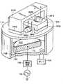
ウエハ上のプラズマ通路の断面積を減少することによってウエハ表面に近くに高プラズマ密度を実現する1つの方法は、ウエハと天井のギャップ長を減少することである。これは、単に天井の高さを減少することによって、または図2に示されるように、ウエハ上に導電性のガス分配プレート、即ちシャワーヘッドを導入することによって達成される。図2のガス分配シャワーヘッド210は、ガス源125に接続され、複数のガスノズル開口230を通してウエハ120上のプロセス領域と連通するガス分配プレナム220からなる。導電性シャワーヘッド210の利点は、2つある。即ち、第1に、そのウエハへの接近した位置によって、シャワーヘッドはウエハ表面上のプラズマ通路を圧縮し、それによりその近傍でプラズマ流の密度を増大する。第2に、シャワーヘッドはウエハの全表面近く及びウエハ表面を横切って、均一な電位規準または接地面を与える。Increasing Plasma Ion Density One way to achieve high plasma density close to the wafer surface by reducing the cross-sectional area of the plasma passage on the wafer is to reduce the gap length between the wafer and the ceiling. This is accomplished simply by reducing the height of the ceiling, or by introducing a conductive gas distribution plate or showerhead over the wafer, as shown in FIG. The
好ましくは、開口230を横切るアークを避けるために、各々の開口230は比較的小さく、ミリメートルのオーダー(好適な孔の直径は約0.5mm)である。隣り合う開口間の間隔は、数ミリメートルのオーダである。 Preferably, each
プラズマシースがプラズマ中に浸されているシャワーヘッドの表面部分の周りに形成されるので、導電性シャワーヘッド210は、それ自体を通して短絡回路を与えることなくプラズマ流通路を絞る。このシースは、ウエハ120とシャワーヘッド210間の空間よりプラズマ流に対して大きなインピーダンスを有し、従って全てのプラズマ流は、導電性シャワーヘッド210の周りに流れる。 Since the plasma sheath is formed around the surface portion of the showerhead that is immersed in the plasma, the
ウエハ上にあるプロセス領域近傍にトロイダルプラズマ流または通路を絞るために、シャワーヘッド(例えば、シャワーヘッド210)を用いることは必要でない。通路の絞り、及びその結果生じる処理領域におけるプラズマイオン密度の増加は、シャワーヘッドを必要とすることなくウエハと天井の高さを単に減少することによって達成される。もし、この方法でシャワーヘッド210が除去されるなら、プロセスガスは従来の入口ノズル(図示せず)によってチャンバ内部に供給されることができる。 It is not necessary to use a showerhead (eg, showerhead 210) to constrict the toroidal plasma flow or path near the process area on the wafer. Passage restriction and the resulting increase in plasma ion density in the processing region is accomplished by simply reducing the height of the wafer and ceiling without the need for a showerhead. If the
シャワーヘッド210の1つの利点は、例えば、ホトレジスト上のプラズマ効果の不均一性を細かく調整するために、反応性と不活性のプロセスガスのいろいろな混合比が異なる半径の異なる開口部230を通して導入されることである。従って、例えば、反応性ガスに対して大きな割合の不活性ガスを中間半径の外側の開口部230に供給することができ、これに対し、不活性ガスに対して大きな割合の反応性ガスを中間半径の内側の開口部230に供給することができる。 One advantage of the
以下に説明されるように、(ウエハ上のプラズマイオン密度を増加するために)トロイダルプラズマ流通路をウエハ上にある処理領域に絞る他の方法は、ウエハ支持ペデスタルに与えられるRFバイアス電力を増加することによって、ウエハ上のプラズマシースの厚さを増加することである。前述したように、プロセス領域を横切るプラズマ流は、ウエハ表面にあるプラズマシースと天井(またはシャワーヘッド)にあるプラズマシースの間に閉じ込められるので、ウエハ表面にあるプラズマシースの厚さを増加することは、必然的にプロセス領域内のトロイダルプラズマ流を減少し、それによって、プロセス領域におけるプラズマイオン密度を増加する。従って、本明細書において後でより詳細に説明されるように、ウエハ支持ペデスタルのRFバイアス電力が増加されるに従って、ウエハ表面近くのプラズマイオン密度は増加される。 As described below, other methods of concentrating the toroidal plasma flow path to a processing region on the wafer (to increase the plasma ion density on the wafer) increase the RF bias power applied to the wafer support pedestal. By doing so, the thickness of the plasma sheath on the wafer is increased. As described above, the plasma flow across the process area is confined between the plasma sheath on the wafer surface and the plasma sheath on the ceiling (or showerhead), thus increasing the thickness of the plasma sheath on the wafer surface. Inevitably reduces the toroidal plasma flow in the process region, thereby increasing the plasma ion density in the process region. Accordingly, as will be described in more detail later herein, as the RF bias power of the wafer support pedestal is increased, the plasma ion density near the wafer surface is increased.
高エッチング速度での高エッチング選択性
本発明は、高密度プラズマを伴って時々生じる好ましくないエッチング選択性の問題を解決する。図1と図2のリアクタは、容量結合プラズマリアクタのエッチング選択性(約7:1)と同程度に高いに酸化シリコンとホトレジストのエッチング選択性を有し、一方、高いエッチング速度を与えることは、誘導結合プラズマリアクタのエッチング速度に近づく。この成功の理由は、図1と図2のリアクタ構造が、ウエハ120上のプラズマ領域にフリーなフッ素の発生率を減少するように、反応性プロセスガス、一般にフルオロカーボンガスの分離の程度を減少することであると考えらる。従って、フルオロカーボンガスから分離した他の種に対してプラズマ中のフリーなフッ素の割合が望ましく減少される。これらの他の種は、フルオロカーボンプロセスガスからプラズマ中に形成され、保護的なポリマーコーティングとしてホトレジスト上に堆積される保護的なカーボンの豊富なポリマー先駆種を含む。それらは、更に、フルオロカーボンプロセスガスからプラズマ中に形成される反応性のないエッチャント種、例えばCFやCF2を含む。フリーなフッ素は、それが二酸化シリコンを攻撃する程度活発にホトレジスト及びその上に形成される保護的なポリマーコーティングを攻撃する傾向にあり、従って、酸素−ホトレジストのエッチング選択性を減少する。他方、反応性のないエッチング種、例えばCFやCF2は、ホトレジスト及びその上に形成される保護的なポリマーコーティングをよりゆっくり攻撃する傾向にあり、従って優れたエッチング選択性を与える。High etch selectivity at high etch rates The present invention solves the problem of undesirable etch selectivity that sometimes occurs with high density plasmas. The reactors of FIGS. 1 and 2 have silicon and photoresist etch selectivity as high as that of a capacitively coupled plasma reactor (about 7: 1), while providing high etch rates. Approach the etching rate of the inductively coupled plasma reactor. The reason for this success is that the reactor structure of FIGS. 1 and 2 reduces the extent of separation of reactive process gases, typically fluorocarbon gases, such that the incidence of free fluorine in the plasma region on
フリーなフッ素に対するプラズマ種の分離の減少は、プラズマ中の反応性ガスの滞留時間を減少することによって、本発明において達成されると考えられる。これは、フルオロカーボンプロセスガス、例えばCFやCF2からプラズマ中に初期に分離したより複雑な種がそれ自身フリーなフッ素を含む簡単な種に最後には分離されるからである。この分離の最終ステップの程度は、プラズマ中のガスの滞留時間に依存する。本明細書において用いられる用語“滞留時間”は、プロセスガスの分子及びその分子から分離した種がワークピース又はウエハ上のプロセス領域に存在する平均時間に相当する。この時間または期間は、プロセス領域への分子の最初の注入から分子及び/又はその分離した結果が処理ゾーンを通して延びる上述した閉じたトロイダル通路に沿ってプロセス領域から外へ通過するまで延びる。It is believed that the reduction of plasma species separation relative to free fluorine is achieved in the present invention by reducing the residence time of the reactive gas in the plasma. This is because the more complex species initially separated into the plasma from fluorocarbon process gases such as CF and CF2 are eventually separated into simple species that themselves contain free fluorine. The degree of this final separation step depends on the residence time of the gas in the plasma. As used herein, the term “residence time” corresponds to the average time a process gas molecule and species separated from the molecule exist in the process area on the workpiece or wafer. This time or period extends from the initial injection of molecules into the process region until the molecules and / or their separation results pass out of the process region along the above-described closed toroidal passage extending through the treatment zone.
上述したように、本発明は、フルオロカーボンのプロセスガスのプロセス領域における滞留時間を減少することによって、エッチングの選択性を増大する。滞留時間の減少は、ウエハ120と天井110間のプラズマボリューム(体積)を絞ることによって達成される。 As discussed above, the present invention increases etch selectivity by reducing the residence time of the fluorocarbon process gas in the process region. Reduction of the residence time is achieved by reducing the plasma volume between the
ウエハから天井までのギャップ、即ちボリュームの減少は、有益な効果を有する。第1に、それはウエハ上のプラズマ密度を増加して、エッチング速度を上昇する。第2に、ボリュームが減少するに従って、滞留時間が下がる。上述したように、本発明は、小さなボリュームを可能にする。従来の誘導結合リアクタと違って、RFソース電力がウエハの上にあるプロセス領域の閉じ込め内にデポジットされないで、むしろ電力デポジションがプラズマ流の全体の閉じたトロイダル通路に沿って分布される。従って、ウエハ−天井間のギャップは、RF誘導磁界の表皮深さ以下にすることができ、実際に、プロセス領域へ導入される反応性ガスの滞留時間を著しく減少するように小さくすることができ、これは著しい効果である。 Reduction of the wafer-to-ceiling gap, or volume, has a beneficial effect. First, it increases the plasma density on the wafer and increases the etch rate. Second, the residence time decreases as the volume decreases. As mentioned above, the present invention allows for small volumes. Unlike conventional inductively coupled reactors, RF source power is not deposited within the process area confinement above the wafer, but rather power deposition is distributed along the entire closed toroidal path of the plasma flow. Thus, the gap between the wafer and the ceiling can be less than or equal to the skin depth of the RF induced magnetic field, and in fact can be reduced to significantly reduce the residence time of the reactive gas introduced into the process area. This is a remarkable effect.
プラズマ通路の断面、従ってウエハ120上のボリュームを減少するのに2つの方法がある。1つは、ウエハからシャワーヘッドまでのギャップ距離を減少することである。他は、上に簡単に説明したように、RFバイアス電力発生器162によってウエハペデスタルに与えられるバイアスRF電力を増加することによって、ウエハ上のプラズマシースの厚さを増加することである。いずれの方法も、発光分光学(optical emission spectroscopy: OES)技術を用いて観測されるウエハの近傍におけるプラズマ中のフリーなフッ素の含有の減少(結果として、誘電体とホトレジストのエッチング選択性の増加)につながる。 There are two ways to reduce the cross-section of the plasma path and thus the volume on the
フリーなフッ素の含有を減少してエッチングの選択性を向上するための、本発明による3つの追加方法がある。1つの方法は、化学的非反応性希釈ガス、例えばアルゴンをプラズマに導入することである。好ましくは、第2のプロセスガス源190から中空導管150ヘアルゴンガスを直接導入することによって、アルゴンガスが外部からプロセス領域上に導入され、一方、化学的反応性プロセスガス(フルオロカーボンガス)は、シャワーヘッド210のみを通してチャンバへ入る。この有利な配置の場合、アルゴンイオン、中性子、及び励起された中性子は、トロイダル通路のプラズマ流内を、新しく導入された反応性ガス(フルオロカーボン)を希釈するためにウエハ表面を横切ってプロセス領域を通って伝播し、それにより、ウエハ上のそれらの滞留時間を効果的に減少する。プラズマのフリーなフッ素含有量を減少する他の方法は、チャンバ圧力を減少することである。さらに他の方法は、コイルアンテナ170に加えるRFソース電力を減少することである。 There are three additional methods according to the present invention to improve the etch selectivity by reducing the content of free fluorine. One method is to introduce a chemically non-reactive diluent gas, such as argon, into the plasma. Preferably, argon gas is introduced into the process region from the outside by introducing argon gas directly from the second
図3は、ウエハ−シャワーヘッド間のギャップ距離が減少されるに従って、プラズマのフリーなフッ素の含有量が減少する、本発明において観察された傾向を示すグラフである。図4は、ウエハペデスタル115に加えられたプラズマバイアス電力を増加することによって、プラズマのフリーなフッ素含有量が減少することを示すグラフである。図5は、コイルアンテナ170に加えられるRFソース電力を減少することによって、プラズマのフリーなフッ素含有量が減少することを示すグラフである。図6は、チャンバ圧力を減少することによって、プラズマのフリーなフッ素含有量が減少することを示すグラフである。図7は、円筒状エンクロージャ150への希釈ガス(アルゴンガス)の流速を増加することによって、プラズマのフリーなフッ素含有量が減少することを示すグラフである。図3−図7のグラフは、いろいろなOES観察から判断されるプラズマの振舞いの傾向を単に概略的に示したもので、実際のデータを示したものではない。 FIG. 3 is a graph showing the trend observed in the present invention where the free fluorine content of the plasma decreases as the gap distance between the wafer and showerhead is decreased. FIG. 4 is a graph showing that increasing the plasma bias power applied to the
本発明の広いプロセスウインドウ
チャンバ圧力は、0.5T以下であり、そして1mT程度に低くすることができる。プロセスガスは、約20mTに維持されるチャンバ圧力を有し、150cc/mのアルゴンと共に約15cc/mの流速でガス分配シャワーヘッドを通してチャンバ100へ導入されるC4F8である。代わりに、アルゴンガスの流速は650cc/mに、またチャンバ圧力は60mTに増加することができる。アンテナ170は、13MHzで約500ワットのRF電力で励起される。ウエハーシャワーヘッド間のギャップは、約0.3〜約2インチである。ウエハペデスタルに加えられるバイアスRF電力は、13MHz、2000ワットである。他の周波数の選択がなされてもよい。コイルアンテナ170に加えられるソース電力は、50KHz程度の低さか、または13MHzの数倍の高さ、或いはそれより高くてもよい。ウエハペデスタルに加えられるバイアス電力についても同じことである。The wide process window chamber pressure of thepresent invention is 0.5T or less and can be as low as 1 mT. The process gas is C4 F8 having a chamber pressure maintained at about 20 mT and introduced into the
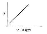
図1と図2のリアクタに対するプロセスウインドウは、従来の誘導結合リアクタに対するプロセスウインドウよりはるかに広い。これは、従来の誘導性リアクタ、及び図1と図2のリアクタに対するRFソース電力の関数としてフリーなフッ素の特定の中性フラックス(neutral flux)を示す図8のグラフに示されている。従来の誘導結合リアクタに対して、図8は、フリーなフッ素の特定のフラックスは、ソース電力が50と100ワット間を越えるに従って、急激に増加し始めることを示している。これに対して、図1と図2のリアクタは、フリーなフッ素の特定なフラックスが急激に増加し始める前に1000ワットに近かいソース電力レベルを受け入れることができる。従って、本発明のソース電力のプロセスウインドウは、従来の誘導結合リアクタのプロセスウインドウよりも広く、これは著しい利点である。 The process window for the reactor of FIGS. 1 and 2 is much wider than the process window for a conventional inductively coupled reactor. This is shown in the graph of FIG. 8 which shows the specific neutral flux of free fluorine as a function of RF source power for the conventional inductive reactor and the reactor of FIGS. For a conventional inductively coupled reactor, FIG. 8 shows that the specific flux of free fluorine begins to increase sharply as the source power exceeds between 50 and 100 watts. In contrast, the reactors of FIGS. 1 and 2 can accept source power levels approaching 1000 watts before the specific flux of free fluorine begins to increase rapidly. Thus, the source power process window of the present invention is wider than the process window of conventional inductively coupled reactors, which is a significant advantage.
本発明の二重の利点
ウエハまたはワークピースの近傍のトロイダルプラズマ流路の閉じ込めは、他の性能基準に対し著しいトレードオフのない2つの独立した利点を有する。(1)ウエハ上のプラズマ密度は、プラズマのソース電力の如何なる増加の必要性もなく増加され、(2)ホトレジストまたは他の材料に対するエッチングの選択性は、上述のように増加される。従来のプラズマリアクタにおいて、エッチングの選択性を増加する同じステップによってプラズマイオン密度を増加することは、不可能ではないにしても実用的ではなかった。従って、本発明のトロイダルプラズマソースによって実現される二重の利点は、従来技術からの革新的な出発であるようである。Dual Advantages of the Invention The confinement of the toroidal plasma flow path in the vicinity of the wafer or workpiece has two independent advantages with no significant trade-off over other performance criteria. (1) The plasma density on the wafer is increased without the need for any increase in the source power of the plasma, and (2) the etch selectivity for photoresist or other materials is increased as described above. In conventional plasma reactors, increasing plasma ion density by the same step of increasing etch selectivity has not been practical if not impossible. Thus, the double advantage realized by the toroidal plasma source of the present invention appears to be an innovative departure from the prior art.
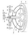
他の好適な実施の形態
図9は、図1の実施の形態のサイドアンテナ170が天井110と中空導管150の間の空間内に収まった小さなアンテナ910によって置き換えられた変形例を示す。好ましくは、このアンテナ910は、中空導管150に関して中央に置かれた単一巻線である。Other Preferred Embodiments FIG. 9 shows a variation in which the
図10と図11は、図1の実施の形態が天井110と中空導管150の間の空間を通して延びる閉じた磁気透過性コア1015の追加によってどのように増大されることができるかを示す。コア1015は、アンテナ170から中空導管150内のプラズマへの誘導結合を増進する。 FIGS. 10 and 11 show how the embodiment of FIG. 1 can be augmented by the addition of a closed magnetically
図11を参照して、インピーダンス整合は、同調キャパシタ1130の両端に接続された、コア1015の周囲に巻かれた二次巻線1120を用いることによって、インピーダンス整合回路175を用いずに達成するすることができる。同調キャパシタ1130の容量は、二次巻線1120をRF電源180の周波数に共振するように選択される。固定同調キャパシタ1130に対して、ダイナミックなインピーダンス整合が周波数同調及び/または順方向動力サーボ制御機構によって設けられてもよい。Referring to FIG. 11, impedance matching is achieved without using
図12は、中空チューブのエンクロージャ1250がリアクタの底部の回りにのび、チャンバの底部にある一対の開口1260、1265を通してチャンバ内部と連通している本発明の実施の形態を示す。コイルアンテナ1270は、図1の実施の形態の方法で中空状のエンクロージャ1250によって与えられたトロイダル通路と一緒に沿っている。図12は、主チャンバの底部に結合された真空ポンプ135を示しているけれども、それは下にある導管1250に結合されてもよい。 FIG. 12 illustrates an embodiment of the invention in which a
図13は、図10、図11の実施の形態の変形例を示し、アンテナ170はコア1015の上方区分を囲む誘導性巻線1320によって置き換えられる。巻線1320は、(導管の下部よりむしろ)導管150の上部にあるコア1015の部分を囲むのが都合よい。しかし、巻線1320はコア1015のどの部分を囲んでもよい。 FIG. 13 shows a variation of the embodiment of FIGS. 10 and 11, where the
図14は、図13の概念の拡張を示し、第2の中空チューブ状のエンクロージャ1450が第1の中空導管150と平行に走っており、第2のトロイダルプラズマ流のための平行トロイダル通路を与える。このチューブ状のエンクロージャ1450は、天井110にあるそれぞれの開口を介してその各々の端部においてチャンバ内部と連通している。磁気コア1470が2つのチューブ状のエンクロージャ150、1450の下で、コイルアンテナを通って延びている。 FIG. 14 shows an extension of the concept of FIG. 13 with a second
図15は、図14の概念の拡張を示し、平行な中空チューブ状のエンクロージャ15a、15b、150c、150dのアレーがリアクタチャンバを通して複数のトロイダルプラズマ流路を提供する。図15の実施の形態において、プラズマイオン密度は、独立のRF電源180a-dによって駆動される、個々の導管150a-dにおいてそれぞれ独立して制御される。個々の円筒状の開いたコア1520a-1520dがそれぞれのコイルアンテナ170a-170d内に分離して挿入される。この実施の形態において、中央からエッジまでの相対的なイオン密度分布が個々のRF電源180A-180dの電力レベルを別々に調整することによって調整される。 FIG. 15 shows an extension of the concept of FIG. 14, where an array of parallel hollow
図16は、図15の実施の形態の変更例を示し、チューブ状のエンクロージャ150a-dのアレーが天井を通さないでリアクタの側壁を通して延びている。図16に示された他の変更例は、チューブ状のエンクロージャ150a-dの全てに隣接する単一の共通な磁気コア1470とその回りを囲むアンテナ170を使用しているので、単一のRFソースがチューブ状のエンクロージャ150a-dの全てにプラズマを励起する。 FIG. 16 shows a variation of the embodiment of FIG. 15 in which an array of
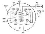
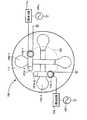
図17Aは、天井110にあるそれぞれのポートを通して延び、それぞれのコイルアンテナ170-aと170−bによって励起される一対の直交したチューブ状エンクロージャ150-1と150-2を示す。それぞれのコア1015-1と1015-2は、それぞれのコイルアンテナ170-aと170-b内にある。この実施の形態は、増大した均一性のために、ウエハ120上方に2つの相互に直交したトロイダルプラズマ流路を形成する。2つの直交したトロイダルまたは閉じた通路は分離され、図示されるように独立して電力が与えられるが、しかしウエハの上にあるプロセス領域において交差しており、その他の点では交差していない。直交した通路の各々1つに与えられるプラズマソース電力の独立した制御を確実にするために、図17のそれぞれのRF発生器180a、180bの周波数は異なっており、その結果インピーダンス整合回路175a、175bの動作は減結合される。例えば、RF発生器180aは、11MHzのRF信号を発生し、RF発生器180bは、12MHzのRF信号を発生することができる。代わりに、2つのRF発生器180a、180bの位相をずらせることによって、独立した動作を達成することができる。 FIG. 17A shows a pair of orthogonal tubular enclosures 150-1 and 150-2 that extend through respective ports in the
図17Bは、ウエハ支持体の上にある処理領域を通して2つの導管150-1、150-2の各々のトロイダルプラズマ流を案内するために、どのようにして放射状の羽根(ベイン)181が用いられるかを示している。放射状の羽根181は、チャンバの横壁近くの各々の導管の開口の問で、ウエハ支持体の端までに延びている。放射状の羽根181は、一方のトロイダル通路から他方のトロイダル通路へのプラズマの発散を防止するので、2つのプラズマ流はウエハの上にある処理領域内でのみ交差する。 FIG. 17B shows how
大きな直径のウエハに適した実施の形態
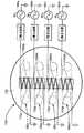
小さなデバイスサイズ及び高いデバイス密度に向かう最近の傾向に加えて、他の傾向は大きなウエハの直径に向かっている。例えば、最近、12インチの直径のウエハが製造されるようになっており、将来的には、恐らくさらに大きな直径のウエハになるであろう。その利点は、ウエハ毎の集積回路のダイの数が非常に大きいために、スループットが大きくなることである。この欠点は、プラズマ処理において、大きな直径のウエハを横切って均一なプラズマを維持することが困難なことである。本発明の以下の実施の形態は、特に大きな直径のウエハ、例えば12インチ直径のウエハの全表面にわたって均一なプラズマイオン密度分布を与えるのに適合されている。Embodiments Suitable for Large Diameter Wafers In addition to the recent trend towards small device size and high device density, other trends are towards large wafer diameters. For example, recently, 12 inch diameter wafers have been manufactured, and in the future, perhaps even larger diameter wafers will be produced. The advantage is increased throughput due to the very large number of integrated circuit dies per wafer. The drawback is that in plasma processing it is difficult to maintain a uniform plasma across a large diameter wafer. The following embodiments of the present invention are particularly adapted to provide a uniform plasma ion density distribution across the entire surface of a large diameter wafer, eg, a 12 inch diameter wafer.
図18と図19は、絶縁ギャップ1852を有する、図1の中空導管150の幅広い扁平な矩形の態様である中空なチューブ状エンクロージャ1850を示す。この態様は、大きな直径のウエハ、例えば12インチ直径のウエハまたはワークピースを一様にカバーするのにより適したプラズマの幅広い“ベルト”を生成する。天井におけるチューブ状エンクロージャ及び一対の開口1860、1862の幅Wは、約5%またはそれ以上ウエハを超えるのが好ましい。例えば、もし、ウエハが10インチであれば、矩形のチューブ状エンクロージャ1850及び開口1860、1862の幅Wは、約11インチである。図20は、図18と図19の矩形のチューブ状エンクロージャ1850の変更態様1850’を示し、外部のチューブ状エンクロージャ1850の一部1864が絞られている。しかし、図18と図19の絞られない態様が好ましい。 FIGS. 18 and 19 illustrate a
図20は、さらに、エンクロージャ1850’の絞られない部分と絞られた部分間の移行部に焦点を絞る磁石1870の選択的使用を示している。焦点を絞る磁石1870は、エンクロージャ1850の絞られない部分と絞られた部分間のプラズマの良好な移動を促進し、特に、プラズマがエンクロージャ1850の絞られない部分と絞られた部分間の移行部を横切って移動するにしたがって、プラズマからのより均一な広がりを促進する。 FIG. 20 further illustrates the selective use of
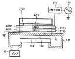
図21は、チューブ状エンクロージャ1850によって囲まれた外側領域2120を通して、複数の円筒状磁気コア2110がどのように挿入されるかを示している。円筒状コア2110は、チューブ状エンクロージャの対称軸にほぼ平行である。図22は、コア2110がチューブ状エンクロージャ1850によって囲まれた外側領域2120を通して完全に延びている図21の実施の形態の変形例を示し、外側領域2120のそれぞれの半分に2対の短くされたコア2210、2220によって置き換えられている。サイドコイル165、185(図1)は、それぞれのコア対2210、2220を囲む一対のコイル巻線2230、2240によって置きかえれている。この実施の形態において、コア対2210、2220間の偏移Dは、ウエハ周辺のイオン密度に対するウエハ中央近くのイオン密度を調整するために変えることができる。広い偏移Dは、ウエハ中央近くの誘導性結合を減少し、従って、ウエハ中央におけるプラズマイオン密度を減少する。従って、ウエハ表面を横切ってイオン密度の空間分布を正確に調整するための追加の制御素子が設けられる。図23は、図22の実施の形態の変形例を示し、別々の巻線2230、2240がコア対2210、2220に対して中央に置かれた単一の中央巻線によって置き換えられている。 FIG. 21 shows how a plurality of cylindrical
図24と図25は、ウエハを横切ってプラズマイオン密度の分布に非常に優れた均一性を与える実施の形態を示す。図24と図25の実施の形態において、互いに横切って、好ましくは、相互に直交している2つのプラズマ流の通路が確立される。これは、第1のチューブ状エンクロージャ1850に対して横切って、好ましくは直交して延びる第2の幅広い矩形の中空エンクロージャ2420を与えることによって達成される。第2のチューブ状エンクロージャ2420は、天井110を通して一対の開口2430、2440を通してチャンバの内部と連通しており、そして絶縁ギャップ2452を有する。第2のチューブ状エンクロージャ2420の側面に沿って一対のサイドコイルの巻線2450、2460がプラズマを維持し、インピーダンス回路2480を介して第2のRF電源2470によって励振される。図24に示されるように、2つの直交プラズマ流がウエハ表面上の空間を同時に占め、ウエハ表面上に均一な範囲のプラズマを与える。この実施の形態は、10インチ及びそれ以上の直径を有する大きなウエハを処理するために特に有利な使用方法を見出すことが期待されている。 24 and 25 show an embodiment that provides very good uniformity in plasma ion density distribution across the wafer. In the embodiment of FIGS. 24 and 25, two plasma flow paths are established across each other, preferably orthogonal to each other. This is accomplished by providing a second wide rectangular
図17の実施の形態におけるように、図24の実施の形態は、均一性を高めるためにウエハ上に2つの相互に直交するトロイダルプラズマを形成する。この2つの直交するトロイダル上の、または閉じた通路は、図示されるように分離され、独立して電力が供給されるが、そうしなければ、相互作用を及ぼし、または互いに発散するか、拡散する。直交する通路のそれぞれの1つに供給されるプラズマソース電力の別々の制御を確実にするために、インピーダンス整合回路の動作が減結合されるように、図24のそれぞれのRF発生器180、2470の周波数は異なる。例えば、RF発生器180は、11MHzのRF信号を発生し、一方、RF発生器2470は、12MHzのRF信号を発生することができる。代わりに、2つのRF発生器180、2470の位相をずらすことによって、独立した動作が達成される。 As in the embodiment of FIG. 17, the embodiment of FIG. 24 forms two mutually orthogonal toroidal plasmas on the wafer to increase uniformity. The two orthogonal toroidal or closed passages are separated as shown and powered independently, otherwise they interact or diverge from each other or diffuse To do. Each
図26は、図18の実施の形態の変形例を示し、絶縁ギャップ2658を有する変更された矩形のエンクロージャ2650が天井110を通ることなくチャンバの側壁105を介してチャンバ内部と連通する。この目的のために、矩形のエンクロージャ2650は水平な上部区分2652、上部区分2652のそれぞれの端において一対の下方に延びる脚2654、及び一対の水平な、内方に延びる脚2656を有し、それぞれが、下方に延びる脚2654のそれぞれの1つの下部端から側壁105にあるそれぞれの開口2670、2680に延びている。 FIG. 26 shows a variation of the embodiment of FIG. 18 in which a modified
図27は、絶縁ギャップ2752を有する第2の矩形チューブ状エンクロージャ2710が図26の実施の形態にどのようにして加えられるかを示している。第2の矩形のチューブ状エンクロージャ2710は、矩形のチューブ状エンクロージャ2650、2710が相互に直交している(または互いに少なくとも横切っている)点を除いて図26の矩形のチューブ状エンクロージャ2650と同一である。第2の矩形のチューブ状エンクロージャは、開口2720を有する側壁105を通してそれぞれの開口を介してチャンバ内部と連通している。図25の実施の形態と同様に、チューブ状エンクロージャ2650、2710は、大きなウエハの直径上に優れた均一性を与えるために、ウエハの表面上に同時に空間を占める相互に直交するトロイダルプラズマ流を生成する。プラズマソース電力は、それぞれ対のサイドコイル巻線165、185、及び2450、2460を介してチューブ状エンクロージャの内部に供給される。 FIG. 27 shows how a second
図28Aは、サイドコイル165、185、2450、2460が2つの矩形のチューブ状エンクロージャ2650、2710によって囲まれる外側領域2860内にある一対の相互に直交する内部コイル2820、2840によってどのように置き換えられる(または、補われる)かを示している。コイル2820、2840の各々の1つが矩形のチューブ状エンクロージャ2650、2710の対応する1つにトロイダルプラズマ流を生成する。これらのコイル2820、2840は異なる周波数で完全に独立して駆動されるか、同じ位相または異なる位相の同一の周波数で駆動されれてもよい。または、それらは、結合されたトロイダルプラズマ流をソース電力周波数で回転させる位相差(即ち、90度)を有する同一周波数で駆動することができる。この場合、コイル2820、2840は、それぞれ、図28Aに示されるように共通の信号発生器2880のサインとコサイン成分で駆動される。この利点は、プラズマ流通路がプラズマイオン周波数を越える回転周波数でウエハ表面を横切って方位角的に回転するので、従来技術の方法、例えば、回転が非常に低い周波数であるMERIEリアクタより不均一性がよく抑制されることである。 FIG. 28A shows how the side coils 165, 185, 2450, 2460 are replaced by a pair of mutually orthogonal
図28Bを参照すると、プラズマイオン密度の半径方向の調整は、一般に、コイル2820内で互いに向かって、または離れて軸方向に移動される一対の磁気円筒状コア2892、2894、及びコイル2840内で互いに向かって、または離れて軸方向に移動される一対の磁気円筒状コア2896、2898によって、与えられる。おのおの一対のコアが互いに向う方向に移動されるに従って、直交プラズマ流の各々の中央近くで誘導性結合がこのプラズマ流の端に対して増強されるので、ウエハ中央におけるプラズマ密度は、一般に増強される。従って中央からエッジまでのプラズマイオン密度は、コア2892、2894、2896、2898を移動することによって制御される。 Referring to FIG. 28B, the radial adjustment of the plasma ion density is generally accomplished within a pair of magnetic
図29は、本発明の他の実施の形態を示し、2つのチューブ状エンクロージャ2650、2710が単一プレナムを構成するリアクタの中心軸の周りに360度広がる単一のエンクロージャ2910へ共に合わされている。図29の実施の形態において、プレナム2190は、下方の半ドーム状壁2920とこの半ドーム状の下方壁2920とほぼ一致する上方の半ドーム状壁2930を有している。従って、プレナム2910は、下方の半ドーム状壁2920と上方の半ドーム状壁2930間の空間である。絶縁ギャップ2921は、上方のドーム状壁2920の周りに広がっており、及び/または絶縁ギャップ2931は、下方のドーム状壁2930の周りに広がっている。プレナム2910は、チャンバの対称軸の周りに360度広がる天井110にある環状の開口2925を介してチャンバ内部と連通している。 FIG. 29 shows another embodiment of the present invention where two
プレナム2910は、天井110の上の領域2950を完全に囲んでいる。図29の実施の形態において、プラズマソース電力は、一対の相互に直交するコイル2960、2965によってプレナム2910の内部に結合される。コイル2960、2965へのアクセスは、プレナム2910の中心を通る垂直の導管2980を通して与えられる。好ましくは、コイル2960、2965は、方位角方向に回転するトロイダルプラズマ流(即ちウエハ面内を回転するプラズマ流)を得るために、図28の実施の形態におけるように、直角位相(quadrature)で駆動される。回転周波数は、供給されたRF電力の周波数である。代わりに、コイル2960、2965は、異なる周波数で別々に駆動されてもよい。図30は、図29の実施の形態の状部断面図である。図31Aと図31Bは、それぞれ図30に相当する前断面図及び側断面図である。 The
1対の相互に直交するコイル2960、2965は、360度/n度離れて配置されたそれらの巻線軸を有する別々に駆動されるコイルの数nによって置き換えられる。例えば、図32は、2つのコイル2960、2965が120度間隔で配置された巻線軸を有する3つのコイル3210、3220、3230によって置き換えられ、インピーダンス整合回路3241、3251、3261を介して3つのRF電源3240、3250、3260によって駆動される場合を示す。回転するトロイダルプラズマ流を生成するために、3つの巻線3210、3220、3230は、図33に示される共通の電源3310から120度ずれた位相で駆動される。図32と図33は、コイル間の相互結合の殆どが垂直導管2980を通ることなく周りにあると考えられるから、2つのコイルのみを有する図29の実施の形態より好適である。 A pair of mutually
図34は、3つのコイルが囲まれた領域2950の外側にある実施の形態を示し、それらの誘導性インダクタンスは、導管2980を通して延びるそれぞれの垂直磁気コア3410によって囲まれた領域2950に結合される。各々のコア3410は、導管2980上に延びる一方の端を有し、その周りにコイル3210、3220、3230のそれぞれの1つが巻かれている。各々のコア340の底は囲まれた領域2950の内部にあり、水平の脚を有する。3つのコア3410の水平の脚は、120度間隔で開かれ、図32の囲まれた領域内の3つのコイルによって与えられた誘導性結合と同様なプレナム2910の内部に誘導性結合を与える。 FIG. 34 shows an embodiment in which three coils are outside the
図18−28の実施の形態の平らな矩形のチューブ状エンクロージャの利点は、チューブ状エンクロージャの広い幅と比較的低い高さがトロイダルプラズマ流を大きな直径のウエハの全表面を容易に覆う、広く薄いベルト状のプラズマにすることである。チューブ状のエンクロージャの全体は最大の幅である必要はない。代わりに、図20の実施の形態について上述したように、チャンバ内部から最も遠いチューブ状のエンクロージャの他の区分が狭くされてもよい。この場合、狭い部分1852を励磁するプラズマ流を広い区分1851の全幅を横切って全体的に広げるために、広い部分1851と狭い部分1852間の移行コーナーにフォーカス磁石1870を設けることが望ましい。もし、ウエハ表面にプラズマイオン密度を最大にすることが必要なら、狭い部分1852の断面積が広い部分1851の断面積と少なくともほぼ同程度に大きいことが望ましい。例えば、狭い部分1852は、その高さと幅がほぼ同じ通路であり、広い部分はその幅より小さい高さを有することができる。 The advantage of the flat rectangular tubular enclosure of the embodiment of FIGS. 18-28 is that the wide width and relatively low height of the tubular enclosure allows the toroidal plasma flow to easily cover the entire surface of a large diameter wafer. It is to make a thin belt-like plasma. The entire tubular enclosure need not be the maximum width. Alternatively, as described above for the embodiment of FIG. 20, other sections of the tubular enclosure furthest from the chamber interior may be narrowed. In this case, it is desirable to provide a
磁気コアを用いる代わりに、空気コアのコイル(即ち、磁気コアのないコイル)を有する、ここで述べたいろいろな実施の形態を用いることができ、そしてそれらは、開いた磁気通路型(Arod@型コア)または添付図面に示された閉じた磁気コア型であることができる。さらに、異なるRF周波数で駆動された2つまたはそれ以上のトロイダル通路を有するここに述べたいろいろな実施の形態は、同じ周波数で駆動されてもよいし、また同じか、または異なる位相で駆動されてもよい。 Instead of using a magnetic core, the various embodiments described herein having an air core coil (ie, a coil without a magnetic core) can be used, and they are open magnetic path types (Arod @ Mold core) or a closed magnetic core mold as shown in the accompanying drawings. Further, the various embodiments described herein having two or more toroidal paths driven at different RF frequencies may be driven at the same frequency and driven at the same or different phases. May be.
図35は、図17の実施の形態の変形例であり、相互に横切る中空導管が図20の実施の形態におけるように狭められている。 FIG. 35 is a variation of the embodiment of FIG. 17, with the hollow conduits traversing each other being narrowed as in the embodiment of FIG.
図36は、図24の実施の形態の変形例であるが、それぞれのRF電源に接続するためにコアの周りにそれぞれの巻線3630、3640を有する1対の磁気コア3610、3620を用いている。 FIG. 36 is a variation of the embodiment of FIG. 24, but using a pair of
図37は、図35の実施の形態に相当する実施の形態であるが、2つのリエントラント導管に代えて、チャンバへの全体で6つのリエントラントポートを有する3つの導管を有している。(図37に示されるように)2つより多い対称に配置された導管及びリエントラントポートを有することは、300mm及びそれより大きな直径のウエハを処理するために特に有利である。 FIG. 37 is an embodiment corresponding to the embodiment of FIG. 35, but instead of two reentrant conduits, it has three conduits with a total of six reentrant ports to the chamber. Having more than two symmetrically arranged conduits and reentrant ports (as shown in FIG. 37) is particularly advantageous for processing 300 mm and larger diameter wafers.
図38は、図35の実施の形態に相当する実施の形態であるが、2つのリエントラント導管に代えて、チャンバへの全体で6つのリエントラントポートを有する3つの導管を有している。 FIG. 38 is an embodiment corresponding to the embodiment of FIG. 35, but instead of two reentrant conduits, it has three conduits with a total of six reentrant ports to the chamber.
図39は、図35の実施の形態に相当する実施の形態であり、外部の導管が共通のプレナム3910において一緒に結合している。 FIG. 39 is an embodiment corresponding to the embodiment of FIG. 35, with external conduits joined together at a
図40は、図36の実施の形態に相当する実施の形態であり、外部の導管が共通のプレナム4010において一緒に結合している。 FIG. 40 is an embodiment corresponding to the embodiment of FIG. 36 with external conduits joined together at a
図41は、図37の実施の形態に相当する実施の形態であり、外部の導管が共通のプレナム4110において一緒に結合している。 FIG. 41 is an embodiment corresponding to the embodiment of FIG. 37 with external conduits joined together at a
図42は、図38の実施の形態に相当する実施の形態であり、外部の導管が共通のプレナム4210において一緒に結合している。 FIG. 42 is an embodiment corresponding to the embodiment of FIG. 38 with external conduits joined together at a
図43は、図17の実施の形態に相当する実施の形態であり、外部の導管が共通のプレナム4310において一緒に結合している。 FIG. 43 is an embodiment corresponding to the embodiment of FIG. 17 with external conduits joined together at a
本発明の有利な特徴
本発明のリアクタは、他の性能の特徴、例えばエッチング速度を犠牲にすることなくエッチングの選択度を増加するためのいろいろな機会を提供する。例えば、ウエハの近傍におけるトロイダルプラズマ流を狭めることは、エッチングの選択度を向上するばかりでなく、同時にプラズマイオン密度を増加することによってエッチング速度を増加する。従来のリアクタは、ワークピース上でエッチング速度またはプラズマイオン密度を増加する同じメカニズムによってエチングの選択度は増加しないと考えられている。Advantageous Features of the Invention The reactor of the present invention offers various opportunities to increase etch selectivity without sacrificing other performance features such as etch rate. For example, narrowing the toroidal plasma flow in the vicinity of the wafer not only improves etch selectivity, but also increases the etch rate by simultaneously increasing the plasma ion density. Conventional reactors are believed not to increase etch selectivity by the same mechanism that increases the etch rate or plasma ion density on the workpiece.
ウエハまたはワークピースの近傍でトロイダルプラズマ流を絞ることによってエッチングの選択度を増加することは、いろいろな方法の1つの本発明において達成することができる。1つの方法は、ペデスタルと天井、即ちウエハと天井の高さを減少することである。他の方法は、トロイダルプラズマイオン流の通路を絞る、ウエハ上にガス分配プレートまたはシャワーヘッドを導入することである。他の方法は、ウエハーまたはワークピースへ供給されるRFバイアス電力を増加することである。エッチングの選択度を増加する前述の方法のいずれか1つまたはいずれかの組合せは、本発明を実行する当業者によって選択することができる。 Increasing etch selectivity by constricting the toroidal plasma flow in the vicinity of the wafer or workpiece can be accomplished in one of several ways in the present invention. One way is to reduce the height of the pedestal and ceiling, ie the wafer and ceiling. Another method is to introduce a gas distribution plate or showerhead on the wafer that constricts the passage of the toroidal plasma ion stream. Another method is to increase the RF bias power supplied to the wafer or workpiece. Any one or any combination of the foregoing methods for increasing etch selectivity can be selected by those skilled in the art practicing the present invention.
本発明において、エッチングの選択度は、さらに、反応性のプロセスガスを局部的(即ち、ウエハまたはワークピース)に注入し、一方、不活性希ガス(例えば、アルゴン)を遠隔的に(即ち、導管またはプレナム)注入するすることによって向上される。これは、ワークピースの支持体上で支持体に面してガス分配プレートまたはシャワーヘッドを直接設け、シャワーヘッドを介して反応性のプロセスガスを排他的に(または少なくとも支配的に)導入することによって達成されるのが好ましい。同時に、希釈ガスは、ウエハまたはワークピースの上にあるプロセス領域から充分離れた導管に注入される。従って、トロイダルプラズマ流は、ウエハ上の材料の反応性イオンエッチングに対してプラズマイオン源になるばかりでなく、さらに、プラズマを誘起した分離プロセスがフリーなフッ素の望ましくない量を形成する点に到達するる前に反応性プロセスガス種及びそれらのプラズマ分離された結果を一掃するためのエージェント(agent)になる。反応性プロセスガス種の滞留時間のこの減少は、ホトレジストおよび他の材料に対してエッチングの選択度を増大し、これは著しい利点である。 In the present invention, the selectivity of the etching is further achieved by injecting a reactive process gas locally (ie, wafer or workpiece) while remotely supplying an inert noble gas (eg, argon) (ie, argon). (Conduit or plenum). This involves providing a gas distribution plate or showerhead directly on the workpiece support facing the support and introducing reactive process gas exclusively (or at least predominantly) through the showerhead Is preferably achieved. At the same time, the dilution gas is injected into a conduit sufficiently away from the process area above the wafer or workpiece. Thus, the toroidal plasma stream not only becomes a plasma ion source for reactive ion etching of materials on the wafer, but also reaches the point where the plasma-induced separation process forms an undesirable amount of free fluorine. It becomes an agent to clean out reactive process gas species and their plasma separated results before doing. This reduction in the residence time of the reactive process gas species increases the selectivity of the etch relative to photoresist and other materials, which is a significant advantage.
本発明は、RFソース電力の、トロイダルプラズマ流への適用において大きなフレキシビリティを与える。上述したように、電力は、一般にアンテナによってトロイダルプラズマ流に誘導結合される。多くの実施の形態において、アンテナは、導管またはプレナムの隣またはその近くにあることによって外部の導管またはプレナムに主に結合される。例えば、コイルアンテナは、アンテナまたはプレナムに並んで広がることができる。しかし、他の実施の形態では、アンテナは、導管またはプレナム、及び主リアクタのエンクロージャ(例えば、天井)間の囲まれた領域に制限される。後者の場合、アンテナは、導管に並ぶのではなく導管の“下”にあると考えることができる。非常に大きなフレキシビリティは、囲まれた領域(導管と主チャンバのエンクロージャの間)を通して延びる1つの磁気コア(複数のコア)および囲まれた領域を越えた拡張部分を有し、そしてこのアンテナはコアの拡張部分に巻かれている実施の形態によって得られる。この実施の形態において、アンテナは、磁気コアを介して誘導結合され、したがって、導管内のトロイダルプラズマ流に隣接する必要はない。この実施の形態において、閉じた磁気コアが用いられ、アンテナはトロイダルプラズマ流または導管からかなり離れているコア区分の周りに巻かれる。したがって、実際に、磁気コアを介してトロイダルプラズマ流にプラズマチャンバを結合することによって、アンテナは殆んどどこに、例えば、プラズマチャンバから全く離れた位置に、配置されてもよい。 The present invention provides great flexibility in the application of RF source power to toroidal plasma flows. As described above, power is typically inductively coupled to the toroidal plasma flow by an antenna. In many embodiments, the antenna is primarily coupled to an external conduit or plenum by being next to or near the conduit or plenum. For example, the coil antenna can extend alongside the antenna or plenum. However, in other embodiments, the antenna is limited to the enclosed area between the conduit or plenum and the main reactor enclosure (eg, ceiling). In the latter case, the antenna can be considered “below” the conduit rather than lined up with the conduit. Very great flexibility has one magnetic core (s) extending through the enclosed area (between the conduit and the main chamber enclosure) and an extension beyond the enclosed area, and this antenna It is obtained by the embodiment wound around the extended part of the core. In this embodiment, the antenna is inductively coupled through the magnetic core and therefore need not be adjacent to the toroidal plasma flow in the conduit. In this embodiment, a closed magnetic core is used and the antenna is wrapped around a core section that is far away from the toroidal plasma flow or conduit. Thus, in practice, the antenna may be placed almost anywhere, for example, quite far from the plasma chamber, by coupling the plasma chamber to the toroidal plasma flow via the magnetic core.
最後に、本発明は、非常に大きな直径のウエハまたはワークピースの表面上にプラズマの均一な範囲を与える。これは、1つの実施の形態では、好ましくは、ウエハの幅を越える幅を有する広いプラズマベルトとしてトロイダルプラズマ流を形成することによって達成される。他の実施の形態では、ウエハ表面を横切るプラズマイオン密度の均一性は、ウエハ上のプロセス領域において2つまたはそれ以上の交差する、相互に横切るかまたは直交するトロイダルプラズマ流を設けることによって得られる。トロイダルプラズマ流の流れは、方向が360/nだけ互いに離れている。トロイダルプラズマ流の各々の1つは、1つのトロイダルプラズマ流の方向に沿って整列された離れたコイルアンテナによってエネルギーが与えられる。1つの好適な実施の形態においては、均一性は、ウエハの上にあるプロセス領域において回転するトロイダルプラズマ流を得るように、それぞれのアンテナへ異なる位相のRF信号を与えることによって増大される。この好適な実施の形態では、最適な構造は、トロイダルプラズマ流が天井または側壁の円形に連続した環状開口を通して主チャンバ部分と連通する円形に連続したプレナムに流れるものである。この後者の特徴は、全体のトロイダルプラズマ流が連続して方位角的に回転することを可能にする。 Finally, the present invention provides a uniform range of plasma on the surface of a very large diameter wafer or workpiece. This is achieved in one embodiment, preferably by forming the toroidal plasma flow as a wide plasma belt having a width that exceeds the width of the wafer. In other embodiments, uniformity of plasma ion density across the wafer surface is obtained by providing two or more intersecting, crossing or orthogonal toroidal plasma flows in the process region on the wafer. . The flow of toroidal plasma flows are separated from each other by a direction of 360 / n. Each one of the toroidal plasma streams is energized by spaced coil antennas aligned along the direction of the one toroidal plasma stream. In one preferred embodiment, the uniformity is increased by providing different phase RF signals to each antenna to obtain a rotating toroidal plasma flow in the process area above the wafer. In this preferred embodiment, the optimal structure is that the toroidal plasma flow flows through a circular continuous plenum that communicates with the main chamber portion through a circular continuous annular opening in the ceiling or sidewall. This latter feature allows the entire toroidal plasma flow to rotate continuously and azimuthally.
本発明は、好適な実施の形態を特に参照して詳細に説明されたけれども、それらの変形及び変更は、本発明の真の精神及び範囲から逸脱することなく作られることを理解すべきである。 Although the invention has been described in detail with particular reference to the preferred embodiments, it is to be understood that these variations and modifications can be made without departing from the true spirit and scope of the invention. .
Claims (18)
Translated fromJapanese基板支持体と、
前記基板支持体に対して間隔をおいて対面する関係にあり、前記基板支持体に隣接する当該チャンバの前記内部環境にプロセスガスを流すように適合された、開口を有するガス分配プレートを含む天井と、
を具備し、
前記ガス分配プレート及び前記基板支持体がそれらの間に基板処理領域を画定し、
さらに、
前記ガス分配プレートに結合された、少なくとも反応性種のプロセスガス源と、
前記ガス分配プレートの対向する両側において、前記天井の各開口を通って前記基板処理領域に連通する端部を有する中空導管であって、該中空導管は前記ガス分配プレートの上に設けられ、該中空導管の内部が前記内部環境を共有するようになっている、中空導管と、
前記導管の一部の周囲に設けられたコアと、該コアの一部の周囲に設けられた誘導性巻線と、該誘導性巻線に結合されたRF電源と、
を具備し、
前記導管が、該導管内に処理ガスのRF磁界による放射を受けて、該導管の前記内部の周りにかつ前記チャンバの前記内部環境内の前記基板処理領域を横切って延びる通路にプラズマを維持する、ように構成されている、
ことを特徴とするプラズマチャンバ。
A plasma chamber defining an evacuated internal environment for processing a substrate, comprising:
A substrate support;
A ceiling that includes a gas distribution plate having an opening that is in spaced relation to the substrate support and is adapted to flow a process gas to the internal environment of the chamber adjacent to the substrate support. When,
Comprising
The gas distribution plate and the substrate support define a substrate processing region therebetween;
further,
A process gas source of at least reactive species coupled to the gas distribution plate;
A hollow conduit having an end communicating with the substrate processing region through each opening in the ceiling on opposite sides of the gas distribution plate, the hollow conduit being provided on the gas distribution plate; A hollow conduit, wherein the interior of the hollow conduit is adapted to share the internal environment;
A core provided around a portion of the conduit; an inductive winding provided around the portion of the core; and an RF power source coupled to the inductive winding;
Comprising
The conduit receives a radiation of an RF magnetic field of process gas in the conduit and maintains a plasma in a passage extending around the interior of the conduit and across the substrate processing region in the interior environment of the chamber. Configured,
A plasma chamber characterized by that.
The plasma chamber according to claim 1, wherein the passage is reentrant.
The plasma chamber according to claim 1, wherein the passage is toroidal.
The plasma chamber of claim 1, wherein the plasma flow circulates around the passage.
The plasma chamber of claim 1, wherein the cross-sectional area of the conduit substantially exceeds the cross-sectional area of the processing region of the substrate.
The plasma chamber of claim 1, wherein the plasma ion density is substantially uniform across the entire substrate support.
The plasma chamber of claim 1, wherein the plasma-induced electric field line extends across the plasma processing region of the substrate from one end of the conduit to the other.
The plasma chamber of claim 7, wherein the electric field lines areparallel .
9. The plasma chamber of claim 8, wherein the electric field strength is uniformly distributed across the plasma processing region of the substrate.
The plasma chamber of claim 1, wherein the conduit has an insulating gap in themiddle between the ends to prevent the conduit from creating a continuous conductive path between the ends.
The plasma chamber of claim 1, wherein the conduit has an outer diameter that issmaller than a diameter of the chamber.
The plasma chamber of claim 1, wherein each end of the conduit has a lateral diameter that is at least as large as the lateral diameter of the substrate support.
The plasma chamber of claim 1, further comprising a bias power source coupled to the substrate support.
The plasma chamber of claim 1, further comprising a gas injection inlet to the conduit.
The plasma of claim 14, wherein the gas inlet is adapted to flow diluent gas, and the gas distribution plate is adapted to flow primarily reactive process gas. Chamber.
The plasma chamber of claim 1, wherein the gas distribution plate is adapted to flow various mixtures of inert and reactive process gases at different radial locations.
The height of the passage along an axis substantially perpendicular to the plane of the substrate support in the substrate processing region is lower than any location in the passage, whereby any plasma ion density in the passage The plasma chamber according to claim 1, wherein a plasma ion density in the substrate processing region is increased as compared with the plasma chamber.
Applications Claiming Priority (15)
| Application Number | Priority Date | Filing Date | Title |
|---|---|---|---|
| US09/636,699US6348126B1 (en) | 2000-08-11 | 2000-08-11 | Externally excited torroidal plasma source |
| US09/637,174US6551446B1 (en) | 2000-08-11 | 2000-08-11 | Externally excited torroidal plasma source with a gas distribution plate |
| US09/638,075 | 2000-08-11 | ||
| US09/638,075US7094316B1 (en) | 2000-08-11 | 2000-08-11 | Externally excited torroidal plasma source |
| US09/636,435US6494986B1 (en) | 2000-08-11 | 2000-08-11 | Externally excited multiple torroidal plasma source |
| US09/636,434 | 2000-08-11 | ||
| US09/637,174 | 2000-08-11 | ||
| US09/636,436 | 2000-08-11 | ||
| US09/636,700 | 2000-08-11 | ||
| US09/636,699 | 2000-08-11 | ||
| US09/636,435 | 2000-08-11 | ||
| US09/636,700US6453842B1 (en) | 2000-08-11 | 2000-08-11 | Externally excited torroidal plasma source using a gas distribution plate |
| US09/636,436US6410449B1 (en) | 2000-08-11 | 2000-08-11 | Method of processing a workpiece using an externally excited torroidal plasma source |
| US09/636,434US6468388B1 (en) | 2000-08-11 | 2000-08-11 | Reactor chamber for an externally excited torroidal plasma source with a gas distribution plate |
| PCT/US2001/025505WO2002015650A2 (en) | 2000-08-11 | 2001-08-13 | Externally excited torroidal plasma source |
Publications (2)
| Publication Number | Publication Date |
|---|---|
| JP2004506339A JP2004506339A (en) | 2004-02-26 |
| JP5204941B2true JP5204941B2 (en) | 2013-06-05 |
Family
ID=27569863
Family Applications (1)
| Application Number | Title | Priority Date | Filing Date |
|---|---|---|---|
| JP2002519385AExpired - LifetimeJP5204941B2 (en) | 2000-08-11 | 2001-08-13 | Toroidal plasma chamber excited from outside |
Country Status (4)
| Country | Link |
|---|---|
| EP (1) | EP1307896A2 (en) |
| JP (1) | JP5204941B2 (en) |
| KR (1) | KR100809889B1 (en) |
| WO (1) | WO2002015650A2 (en) |
Families Citing this family (24)
| Publication number | Priority date | Publication date | Assignee | Title |
|---|---|---|---|---|
| US6939434B2 (en)* | 2000-08-11 | 2005-09-06 | Applied Materials, Inc. | Externally excited torroidal plasma source with magnetic control of ion distribution |
| US7223676B2 (en)* | 2002-06-05 | 2007-05-29 | Applied Materials, Inc. | Very low temperature CVD process with independently variable conformality, stress and composition of the CVD layer |
| US7430984B2 (en)* | 2000-08-11 | 2008-10-07 | Applied Materials, Inc. | Method to drive spatially separate resonant structure with spatially distinct plasma secondaries using a single generator and switching elements |
| KR100542740B1 (en)* | 2002-11-11 | 2006-01-11 | 삼성전자주식회사 | Method and apparatus for generating gas plasma, gas composition for plasma generation and method for manufacturing semiconductor device using same |
| JP4657620B2 (en)* | 2004-04-13 | 2011-03-23 | 株式会社日立ハイテクノロジーズ | Plasma processing equipment |
| WO2006099438A1 (en)* | 2005-03-15 | 2006-09-21 | Varian Semiconductor Equipment Associates, Inc. | Profile adjustment in plasma ion implantation |
| FR2886051B1 (en)* | 2005-05-20 | 2007-08-10 | Commissariat Energie Atomique | METHOD FOR DETACHING THIN FILM |
| ATE543199T1 (en)* | 2005-05-23 | 2012-02-15 | New Power Plasma Co Ltd | PLASMA CHAMBER WITH DISCHARGE INDUCING BRIDGE |
| JP5257917B2 (en)* | 2006-04-24 | 2013-08-07 | 株式会社ニューパワープラズマ | Inductively coupled plasma reactor with multiple magnetic cores |
| US7732309B2 (en)* | 2006-12-08 | 2010-06-08 | Applied Materials, Inc. | Plasma immersed ion implantation process |
| US7871828B2 (en)* | 2007-02-06 | 2011-01-18 | Applied Materials, Inc. | In-situ dose monitoring using optical emission spectroscopy |
| RU2007105087A (en)* | 2007-02-12 | 2008-08-20 | Борис Федорович Полторацкий (RU) | PLASMA ENERGY CONVERTER AND ELECTROMAGNETIC VORTEX REACTOR FOR ITS IMPLEMENTATION |
| US7989329B2 (en)* | 2007-12-21 | 2011-08-02 | Applied Materials, Inc. | Removal of surface dopants from a substrate |
| US7968439B2 (en)* | 2008-02-06 | 2011-06-28 | Applied Materials, Inc. | Plasma immersion ion implantation method using a pure or nearly pure silicon seasoning layer on the chamber interior surfaces |
| US7713757B2 (en)* | 2008-03-14 | 2010-05-11 | Applied Materials, Inc. | Method for measuring dopant concentration during plasma ion implantation |
| US8742665B2 (en)* | 2009-11-18 | 2014-06-03 | Applied Materials, Inc. | Plasma source design |
| JP2011040786A (en)* | 2010-10-25 | 2011-02-24 | Hitachi High-Technologies Corp | Plasma treatment apparatus |
| KR101241049B1 (en) | 2011-08-01 | 2013-03-15 | 주식회사 플라즈마트 | Plasma generation apparatus and plasma generation method |
| MY187052A (en)* | 2013-03-15 | 2021-08-27 | Plasmability Llc | Toroidal plasma processing apparatus |
| JP2015215942A (en)* | 2014-05-07 | 2015-12-03 | 国立大学法人金沢大学 | Plasma generating apparatus and plasma generating method |
| TWI670749B (en)* | 2015-03-13 | 2019-09-01 | 美商應用材料股份有限公司 | Plasma source coupled to a process chamber |
| JP2018522370A (en) | 2015-05-21 | 2018-08-09 | プラズマビリティー, エルエルシー | Toroidal plasma processing equipment with molded workpiece holder |
| JP2022007611A (en)* | 2020-06-26 | 2022-01-13 | 東京エレクトロン株式会社 | Device for forming plasma, device for processing substrate, and method for forming plasma |
| US12284747B2 (en) | 2023-03-07 | 2025-04-22 | Finesse Technology Co., Ltd. | Hollow cathode discharge assistant transformer coupled plasma source and operation method of the same |
Family Cites Families (6)
| Publication number | Priority date | Publication date | Assignee | Title |
|---|---|---|---|---|
| US4431898A (en)* | 1981-09-01 | 1984-02-14 | The Perkin-Elmer Corporation | Inductively coupled discharge for plasma etching and resist stripping |
| US5290382A (en)* | 1991-12-13 | 1994-03-01 | Hughes Aircraft Company | Methods and apparatus for generating a plasma for "downstream" rapid shaping of surfaces of substrates and films |
| US5542559A (en) | 1993-02-16 | 1996-08-06 | Tokyo Electron Kabushiki Kaisha | Plasma treatment apparatus |
| US6150628A (en)* | 1997-06-26 | 2000-11-21 | Applied Science And Technology, Inc. | Toroidal low-field reactive gas source |
| JPH11135297A (en)* | 1997-10-31 | 1999-05-21 | Kumagai Hiromi | Plasma generator |
| KR20020029743A (en)* | 1999-08-06 | 2002-04-19 | 로버트 엠. 포터 | Inductively coupled ring-plasma source apparatus for processing gases and materials and method thereof |
- 2001
- 2001-08-13KRKR1020037002020Apatent/KR100809889B1/ennot_activeExpired - Fee Related
- 2001-08-13JPJP2002519385Apatent/JP5204941B2/ennot_activeExpired - Lifetime
- 2001-08-13EPEP01964028Apatent/EP1307896A2/ennot_activeWithdrawn
- 2001-08-13WOPCT/US2001/025505patent/WO2002015650A2/enactiveApplication Filing
Also Published As
| Publication number | Publication date |
|---|---|
| WO2002015650A2 (en) | 2002-02-21 |
| JP2004506339A (en) | 2004-02-26 |
| KR20030029130A (en) | 2003-04-11 |
| EP1307896A2 (en) | 2003-05-07 |
| WO2002015650A3 (en) | 2002-06-20 |
| KR100809889B1 (en) | 2008-03-06 |
Similar Documents
| Publication | Publication Date | Title |
|---|---|---|
| JP5204941B2 (en) | Toroidal plasma chamber excited from outside | |
| US6348126B1 (en) | Externally excited torroidal plasma source | |
| US6453842B1 (en) | Externally excited torroidal plasma source using a gas distribution plate | |
| US6494986B1 (en) | Externally excited multiple torroidal plasma source | |
| US6468388B1 (en) | Reactor chamber for an externally excited torroidal plasma source with a gas distribution plate | |
| US6410449B1 (en) | Method of processing a workpiece using an externally excited torroidal plasma source | |
| US6551446B1 (en) | Externally excited torroidal plasma source with a gas distribution plate | |
| US6939434B2 (en) | Externally excited torroidal plasma source with magnetic control of ion distribution | |
| US7094316B1 (en) | Externally excited torroidal plasma source | |
| US7430984B2 (en) | Method to drive spatially separate resonant structure with spatially distinct plasma secondaries using a single generator and switching elements | |
| US5938883A (en) | Plasma processing apparatus | |
| JP3691528B2 (en) | High density plasma CVD and etching reactor | |
| US5904780A (en) | Plasma processing apparatus | |
| US7137354B2 (en) | Plasma immersion ion implantation apparatus including a plasma source having low dissociation and low minimum plasma voltage | |
| US5824605A (en) | Gas dispersion window for plasma apparatus and method of use thereof | |
| JP4246477B2 (en) | Plasma processing equipment for spatial control of dissociation and ionization. | |
| JPH04290428A (en) | Plasma reactor using uhf/vhf resonance antenna supply source and method therefor | |
| US20070017897A1 (en) | Multi-frequency plasma enhanced process chamber having a toroidal plasma source | |
| US7320734B2 (en) | Plasma immersion ion implantation system including a plasma source having low dissociation and low minimum plasma voltage | |
| US6136140A (en) | Plasma processing apparatus | |
| KR100391063B1 (en) | Device and Method for Generating Capacitively Coupled Plasma Enhanced Inductively Coupled Plasma | |
| KR100404723B1 (en) | Device for Generating Inductively Coupled Plasma with Lower Aspect Ratio | |
| TW202516572A (en) | Immersed plasma source and process chamber for large area substrates | |
| USRE40963E1 (en) | Method for plasma processing by shaping an induced electric field | |
| JP2635267C (en) |
Legal Events
| Date | Code | Title | Description |
|---|---|---|---|
| A621 | Written request for application examination | Free format text:JAPANESE INTERMEDIATE CODE: A621 Effective date:20080711 | |
| A977 | Report on retrieval | Free format text:JAPANESE INTERMEDIATE CODE: A971007 Effective date:20110415 | |
| A131 | Notification of reasons for refusal | Free format text:JAPANESE INTERMEDIATE CODE: A131 Effective date:20110421 | |
| A521 | Request for written amendment filed | Free format text:JAPANESE INTERMEDIATE CODE: A523 Effective date:20110711 | |
| A131 | Notification of reasons for refusal | Free format text:JAPANESE INTERMEDIATE CODE: A131 Effective date:20120112 | |
| A601 | Written request for extension of time | Free format text:JAPANESE INTERMEDIATE CODE: A601 Effective date:20120412 | |
| A602 | Written permission of extension of time | Free format text:JAPANESE INTERMEDIATE CODE: A602 Effective date:20120419 | |
| A601 | Written request for extension of time | Free format text:JAPANESE INTERMEDIATE CODE: A601 Effective date:20120514 | |
| A602 | Written permission of extension of time | Free format text:JAPANESE INTERMEDIATE CODE: A602 Effective date:20120521 | |
| A521 | Request for written amendment filed | Free format text:JAPANESE INTERMEDIATE CODE: A523 Effective date:20120712 | |
| A131 | Notification of reasons for refusal | Free format text:JAPANESE INTERMEDIATE CODE: A131 Effective date:20120919 | |
| A521 | Request for written amendment filed | Free format text:JAPANESE INTERMEDIATE CODE: A523 Effective date:20121219 | |
| TRDD | Decision of grant or rejection written | ||
| A01 | Written decision to grant a patent or to grant a registration (utility model) | Free format text:JAPANESE INTERMEDIATE CODE: A01 Effective date:20130131 | |
| A61 | First payment of annual fees (during grant procedure) | Free format text:JAPANESE INTERMEDIATE CODE: A61 Effective date:20130218 | |
| R150 | Certificate of patent or registration of utility model | Free format text:JAPANESE INTERMEDIATE CODE: R150 Ref document number:5204941 Country of ref document:JP Free format text:JAPANESE INTERMEDIATE CODE: R150 | |
| FPAY | Renewal fee payment (event date is renewal date of database) | Free format text:PAYMENT UNTIL: 20160222 Year of fee payment:3 | |
| R250 | Receipt of annual fees | Free format text:JAPANESE INTERMEDIATE CODE: R250 | |
| R250 | Receipt of annual fees | Free format text:JAPANESE INTERMEDIATE CODE: R250 | |
| R250 | Receipt of annual fees | Free format text:JAPANESE INTERMEDIATE CODE: R250 | |
| R250 | Receipt of annual fees | Free format text:JAPANESE INTERMEDIATE CODE: R250 | |
| R250 | Receipt of annual fees | Free format text:JAPANESE INTERMEDIATE CODE: R250 | |
| R250 | Receipt of annual fees | Free format text:JAPANESE INTERMEDIATE CODE: R250 | |
| EXPY | Cancellation because of completion of term |