JP5204171B2 - Electrical component and manufacturing method thereof - Google Patents
Electrical component and manufacturing method thereofDownload PDFInfo
- Publication number
- JP5204171B2 JP5204171B2JP2010188664AJP2010188664AJP5204171B2JP 5204171 B2JP5204171 B2JP 5204171B2JP 2010188664 AJP2010188664 AJP 2010188664AJP 2010188664 AJP2010188664 AJP 2010188664AJP 5204171 B2JP5204171 B2JP 5204171B2
- Authority
- JP
- Japan
- Prior art keywords
- film
- layer
- thermal expansion
- expansion coefficient
- sio
- Prior art date
- Legal status (The legal status is an assumption and is not a legal conclusion. Google has not performed a legal analysis and makes no representation as to the accuracy of the status listed.)
- Expired - Fee Related
Links
Images


Classifications
- B—PERFORMING OPERATIONS; TRANSPORTING
- B81—MICROSTRUCTURAL TECHNOLOGY
- B81C—PROCESSES OR APPARATUS SPECIALLY ADAPTED FOR THE MANUFACTURE OR TREATMENT OF MICROSTRUCTURAL DEVICES OR SYSTEMS
- B81C1/00—Manufacture or treatment of devices or systems in or on a substrate
- B81C1/00015—Manufacture or treatment of devices or systems in or on a substrate for manufacturing microsystems
- B81C1/00261—Processes for packaging MEMS devices
- B81C1/00333—Aspects relating to packaging of MEMS devices, not covered by groups B81C1/00269 - B81C1/00325
- B—PERFORMING OPERATIONS; TRANSPORTING
- B81—MICROSTRUCTURAL TECHNOLOGY
- B81C—PROCESSES OR APPARATUS SPECIALLY ADAPTED FOR THE MANUFACTURE OR TREATMENT OF MICROSTRUCTURAL DEVICES OR SYSTEMS
- B81C2203/00—Forming microstructural systems
- B81C2203/01—Packaging MEMS
- B81C2203/0136—Growing or depositing of a covering layer
- B—PERFORMING OPERATIONS; TRANSPORTING
- B81—MICROSTRUCTURAL TECHNOLOGY
- B81C—PROCESSES OR APPARATUS SPECIALLY ADAPTED FOR THE MANUFACTURE OR TREATMENT OF MICROSTRUCTURAL DEVICES OR SYSTEMS
- B81C2203/00—Forming microstructural systems
- B81C2203/01—Packaging MEMS
- B81C2203/0145—Hermetically sealing an opening in the lid
- H—ELECTRICITY
- H01—ELECTRIC ELEMENTS
- H01L—SEMICONDUCTOR DEVICES NOT COVERED BY CLASS H10
- H01L23/00—Details of semiconductor or other solid state devices
- H01L23/28—Encapsulations, e.g. encapsulating layers, coatings, e.g. for protection
- H01L23/31—Encapsulations, e.g. encapsulating layers, coatings, e.g. for protection characterised by the arrangement or shape
- H01L23/3157—Partial encapsulation or coating
- H01L23/3171—Partial encapsulation or coating the coating being directly applied to the semiconductor body, e.g. passivation layer
- H—ELECTRICITY
- H01—ELECTRIC ELEMENTS
- H01L—SEMICONDUCTOR DEVICES NOT COVERED BY CLASS H10
- H01L2924/00—Indexing scheme for arrangements or methods for connecting or disconnecting semiconductor or solid-state bodies as covered by H01L24/00
- H01L2924/0001—Technical content checked by a classifier
- H01L2924/0002—Not covered by any one of groups H01L24/00, H01L24/00 and H01L2224/00
Landscapes
- Engineering & Computer Science (AREA)
- Microelectronics & Electronic Packaging (AREA)
- Manufacturing & Machinery (AREA)
- Micromachines (AREA)
Description
Translated fromJapanese本発明の実施形態は、電気部品およびその製造方法に関する。 Embodiments described herein relate generally to an electrical component and a manufacturing method thereof.
MEMS(Micro Electro Mechanical Systems)デバイスの特徴は、通常の半導体デバイスと異なり、機械的可動部分を有するデバイスであるという点である。したがって、MEMSデバイスを実装する際には、機械的可動部分の動作空間としてキャビティ(空洞)が必要である。すなわち、MEMSデバイスにおいて、中空構造を形成する実装技術/パッケージが用いられる。 A feature of a micro electro mechanical systems (MEMS) device is that it is a device having a mechanically movable part unlike a normal semiconductor device. Therefore, when mounting a MEMS device, a cavity is required as an operation space of the mechanically movable part. That is, in the MEMS device, a mounting technique / package for forming a hollow structure is used.
信頼性の高い電気部品およびその製造方法を提供する。 A highly reliable electrical component and a manufacturing method thereof are provided.
本実施形態による電気部品は、基板と、前記基板上に形成された機能素子と、前記基板上において前記機能素子を収納するキャビティを形成し、複数の貫通孔を有する第1層と、前記第1層上に形成され、複数の前記貫通孔を塞ぐ第2層と、を具備し、前記第1層は、下部側に形成された第1膜と、前記第1膜上に形成され、前記第1膜より熱膨張係数が小さい第2膜と、を含む。 The electrical component according to the present embodiment includes a substrate, a functional element formed on the substrate, a cavity for housing the functional element on the substrate, a first layer having a plurality of through holes, and the first layer. A second layer that is formed on one layer and closes the plurality of through-holes, and the first layer is formed on the first film, a first film formed on a lower side, and And a second film having a smaller coefficient of thermal expansion than the first film.
本実施形態を以下に図面を参照して説明する。図面において、同一部分には同一の参照符号を付す。 The present embodiment will be described below with reference to the drawings. In the drawings, the same parts are denoted by the same reference numerals.
<第1の実施形態>
図1乃至図5を用いて第1の実施形態に係る電気部品について説明する。第1の実施形態は、薄膜ドームとして形成される開口を有する第1層が熱膨張係数(CTE:Coefficient of Thermal Expansion)の異なる2膜で形成される例である。<First Embodiment>
The electrical component according to the first embodiment will be described with reference to FIGS. The first embodiment is an example in which a first layer having an opening formed as a thin film dome is formed of two films having different coefficients of thermal expansion (CTE).
[構造]
図1は、第1の実施形態に係る電気部品の断面図を示している。[Construction]
FIG. 1 shows a cross-sectional view of an electrical component according to the first embodiment.
図1に示すように、本実施形態に係る電気部品は、機能素子120を有する基板100、第1層109、第2層110、および第3層111で構成されている。 As shown in FIG. 1, the electrical component according to this embodiment includes a
基板100は、例えばシリコン基板である。この基板100上に、例えばSiO(SiO2)膜(シリコン酸化膜)で構成される絶縁膜101が形成されている。この絶縁膜101上に機能素子120が形成されている。機能素子120は、例えば静電駆動型のMEMS可変容量キャパシタである。The
機能素子120は、第1金属配線102と、第1金属配線102に対向する第2金属配線106と、第2金属配線106同士を接続する絶縁体接続部107とで構成されている。第1金属配線102および第2金属配線106は、例えばアルミニウムで構成されている。絶縁体接続部107は、例えばSiN膜で構成されている。機能素子120は、第1金属配線102と第2金属配線106との間に電圧を印加すると、静電引力によって第1金属配線102と第2金属配線106との間の距離が変化することにより容量が変化する。 The
第1金属配線102上には、例えばSiO(SiO2)膜、またはSiN膜で構成されるパッシベーション膜104が形成されている。このパッシベーション膜104は、パッド部分104aおよび接続孔部分104bに開口を有している。パッド部分104aは、後述する第3層111の外側に形成され、図示せぬ外部電極と電気的に接続されている。すなわち、機能素子120は、パッド部分104aを介して外部電極と電気的に接続されている。また、接続孔部分104bにおいて、第1金属配線102と第2金属配線106とが電気的に接続されている。A
機能素子120は、キャビティ130内に形成されている。このキャビティ130は、機能素子120の動作空間を確保するための領域である。キャビティ130内は、乾燥雰囲気、または真空雰囲気に保たれている。このため、有害ガス、例えば水分によって、アルミニウムで構成される第1金属配線102および第2金属配線106が劣化することが防止され、MEMS可変容量キャパシタの特性劣化が防止されている。 The
第1層109は、機能素子120を収納するキャビティ130を形成し、複数の貫通孔(開口)109cを有する。この第1層109は、機能素子120を外部から保護するための薄膜ドームとして機能する。 The
第1層109の複数の貫通孔109cは、機能素子120を形成した後、後述する犠牲層をエッチングして除去し、キャビティ130を形成するためのものである。すなわち、犠牲層は、貫通孔109cを通してエッチングされる。 The plurality of through
この第1層109の詳細については、後述する。 Details of the
第2層110は、第1層109上に形成され、複数の貫通孔109cを塞いでいる。この第2層110は、キャビティ130を封止しながら、キャビティ130内の有害ガスを透過させて排出し、キャビティ130内の雰囲気を調整する機能を有している。 The
第2層110は、ポリイミド等の有機材料の塗布膜で構成されていることが望ましい。これにより、貫通孔109cのサイズ(直径または開口面積)が大きくても、貫通孔109cを容易かつ確実に封止することができる。したがって、貫通孔109cのサイズや配置が制約されない。このため、サイズの大きい複数の貫通孔109cを配置することにより、後述する犠牲層のエッチングを短時間で確実に行うことが可能である。 The
なお、第2層110は、有機材料の塗布膜に限らず、SiO(SiO2)膜、SiN膜等の絶縁膜で構成されてもよい。The
第3層111は、第2層110上に形成されている。この第3層111は、大気中の水分が第2層110を透過してキャビティ130内に浸入することを防止する防湿膜として機能する。第3層111は、例えばSiN膜等の絶縁膜で構成されている。 The
以下に、本実施形態における第1層109について説明する。本実施形態における第1層109は、内側(下部側)の第1膜109aと、第1膜109a上に形成された外側(上部側)の第2膜109bとの積層膜で構成されている。 Below, the
より具体的には、第1膜109aの熱膨張係数は、第2膜109bの熱膨張係数より大きい。すなわち、貫通孔109cを有する第1層109において、内側の熱膨張係数が外側の熱膨張係数より大きくなる。 More specifically, the thermal expansion coefficient of the
ここで、第1膜109aは例えばSiN膜で構成され、第2膜109bは例えばSiO(SiO2)膜で構成される。このように、第1層109として、熱膨張係数の異なる2層を形成し、かつ内側の第1膜109aの熱膨張係数を第2膜109bの熱膨張係数よりも大きくすることで、薄膜ドームが外側に膨らむ構造にすることができる。すなわち、キャビティ130内が大きく形成される。Here, the
なお、第1膜109aと第2膜109bの組み合わせとして、SiN膜とSiO(SiO2)膜に限らない。これ以外の第1膜109aと第2膜109bの組み合わせとして、熱膨張係数が大きいSiN膜と熱膨張係数が小さいSiN膜、または熱膨張係数が大きいSiO(SiO2)膜と熱膨張係数が小さいSiO(SiO2)膜等が挙げられる。また、SiO(SiO2)膜の熱膨張係数がSiN膜の熱膨張係数よりも大きければ、第1膜109aをSiO(SiO2)膜とし、第2膜109bをSiN膜としてもよい。このような熱膨張係数は、後述する製造方法によって、適宜制御することが可能である。Note that the combination of the
また、SiN膜は、防湿性が高く、大気の水分の浸透を抑制する。このため、第1膜109aおよび第2膜109bのどちらか一方がSiN膜であることがより望ましい。 Further, the SiN film has high moisture resistance and suppresses the penetration of moisture in the atmosphere. Therefore, it is more desirable that one of the
また、第2層110および第3層111の熱膨張係数は、第1層109の熱膨張係数より小さいことが望ましい。これにより、薄膜ドームが外側により膨らむ構造にすることができる。 In addition, the thermal expansion coefficients of the
[製造方法]
図2乃至図4は、第1の実施形態に係る電気部品の製造工程における断面図を示している。以下に、第1の実施形態に係る電気部品におけるMEMS素子の形成工程〜ウェハレベルの薄膜ドームの形成工程を説明する。[Production method]
2 to 4 show cross-sectional views in the manufacturing process of the electrical component according to the first embodiment. Below, the formation process of the MEMS element in the electrical component which concerns on 1st Embodiment-the formation process of the thin film dome of a wafer level is demonstrated.
まず、図2(a)に示すように、MEMS素子の形成工程において、基板100上に、例えばSiO(SiO2)膜で構成される絶縁膜101が形成される。この絶縁膜101上に、例えばアルミニウムで構成される第1金属配線102が形成され、パターニングされる。この第1金属配線102は、膜厚が例えば数百nm〜数μmで形成される。第1金属配線102の成膜方法としてはスパッタリング法が用いられる。また、パターニング方法としては従来のフォトリソグラフィ法とRIE(Reactive Ion Etching)法が用いられてもよいし、フォトリソグラフィとウェットエッチング法が用いられてもよい。なお、絶縁膜101は形成されなくてもよく、その場合、第1金属配線102は、基板100上に直接形成される。First, as shown in FIG. 2A, an insulating
次に、全面に、例えばSiO(SiO2)、またはSiN膜で構成されるパッシベーション膜104が形成される。パッシベーション膜104の成膜方法としては、例えばCVD(Chemical Vapor Deposition)法が用いられる。このパッシベーション膜104は、膜厚が例えば数百nm〜数μmで形成される。その後、パッシベーション膜104がパターニングされ、パッド部分104aおよび接続孔部分104bが開口される。すなわち、パッド部分104aおよび接続孔部分104bの第1金属配線102が露出される。パッシベーション膜104のパターニング方法としては、例えばフォトリソグラフィ法とRIE法が用いられる。Next, a
次に、図2(b)に示すように、第1金属配線102を覆うように、ポリイミド等の有機材料で構成される第1犠牲層105が塗布される。この第1犠牲層105は、膜厚が例えば数百nm〜数μmで形成される。 Next, as shown in FIG. 2B, a first
その後、第1犠牲層105が所望の形状にパターニングされる。これにより、パッド部分104aおよび接続孔部分104bの第1金属配線102が露出される。第1犠牲層105は、感光露光および現像によりパターニングされてもよい。または、第1犠牲層105上に通常のリソグラフィ法で形成された図示せぬレジストパターンとRIE法より、第1犠牲層105がパターニングされてもよい。または、第1犠牲層105上に形成された図示せぬSiO膜等を通常のリソグラフィ法によるレジストパターンとRIE法あるいはウェットエッチング法によってハードマスクとしてパターニングし、このハードマスクを用いて第1犠牲層105がパターニングされてもよい。 Thereafter, the first
次に、図2(c)に示すように、第1犠牲層105上に、例えばアルミニウムで構成される第2金属配線106が形成され、パターニングされる。この第2金属配線106は、膜厚が例えば数百nm〜数μmで形成される。これにより、第2金属配線106は、露出された接続孔部分104bの第1金属配線102と接続される。第2金属配線106の成膜方法としてはスパッタリング法が用いられる。また、パターニング方法としてはフォトリソグラフィ法とRIE法が用いられてもよいし、フォトリソグラフィとウェットエッチング法が用いられてもよい。 Next, as shown in FIG. 2C, a
次に、図3(a)に示すように、第2金属配線106間に、例えばSiN膜で構成される絶縁体接続部107が形成され、パターニングされる。絶縁体接続部107は、膜厚が例えば数百nm〜数μmで形成される。これにより、第2金属配線106同士が接続される。絶縁体接続部107の成膜方法およびパターニング方法としては、従来の半導体技術が用いられる。このようにして、可動部となるMEMS素子120が完成する。 Next, as shown in FIG. 3A, an
次に、図3(b)に示すように、ウェハレベルの薄膜ドームの形成工程において、MEMS素子120および第1犠牲層105を覆うように、ポリイミド等の有機材料で構成される第2犠牲層108が塗布される。この第2犠牲層108は、膜厚が例えば数百nm〜数μmで形成される。 Next, as shown in FIG. 3B, in the step of forming the wafer level thin film dome, the second sacrificial layer made of an organic material such as polyimide so as to cover the
その後、第2犠牲層108が所望の形状にパターニングされる。第2犠牲層108は、感光露光および現像によりパターニングされてもよい。または、第2犠牲層108上に通常のリソグラフィ法で形成された図示せぬレジストパターンとRIE法により、第2犠牲層108がパターニングされてもよい。または、第2犠牲層108上に形成された図示せぬSiO膜等を通常のリソグラフィ法によるレジストパターンとRIE法あるいはウェットエッチング法によってハードマスクとしてパターニングし、このハードマスクを用いて第2犠牲層108がパターニングされてもよい。 Thereafter, the second
次に、図3(c)に示すように、第2犠牲層108を覆うように、複数の貫通孔109cを有する第1層109が形成される。 Next, as shown in FIG. 3C, a
より具体的には、まず、第2犠牲層108を覆うように、薄膜ドームの内側となる第1膜109aが形成される。第1膜109aは、膜厚が例えば数百nm〜数μmで形成される。また、第1膜109aは、例えばSiN膜で構成されている。第1膜109aの成膜方法としては、CVD法が用いられる。このCVD法の条件として、例えばSiH4ガスの流量500sccm、NH3ガスの流量2slm、圧力5Torr、温度400℃とする。また、RF出力を500〜2000Wとする。More specifically, first, a
次に、第1膜109a上に、薄膜ドームの外側となる第2膜109bが形成される。第2膜109bは、膜厚が例えば数百nm〜数μmで形成される。また、第2膜109bは、例えばSiO(SiO2)膜で構成されている。この第2膜109bは、第1膜109aよりも熱膨張係数が小さくなるように制御される。第2膜109bの成膜方法としては、CVD法が用いられる。このCVD法の条件として、例えばSiH4ガスの流量200sccm、N2Oガスの流量4slm、圧力3Torr、温度400℃とする。また、RF出力を200〜1000Wとする。Next, a
次に、第2膜109b上に、図示せぬレジストが塗布される。その後、通常のリソグラフィ法で形成された図示せぬレジストパターンとRIE法またはウェットエッチング法により、薄膜ドームの内側膜(第1膜109a)および外側膜(第2膜109b)に第1犠牲層105および第2犠牲層108除去用の複数の貫通孔109cが開口される。 Next, a resist (not shown) is applied on the
このとき、図示せぬレジストパターンと第1層109との選択比を調整することにより、貫通孔109cの形状が、外側から内側に向かって次第に径が大きくなることが望ましい。言い換えると、貫通孔109cの形状が外側から内側に向かって次第に径が小さくなるテーパー形状であることが望ましい。これは、後述する第1犠牲層105および第2犠牲層108を除去した後に、貫通孔109cの封止特性を向上させるためである。 At this time, it is desirable that the diameter of the through
このようにして、熱膨張係数が大きい内側の第1膜109aと、それより熱膨張係数が小さい内側の第2膜109bとで構成され、複数の貫通孔109cを有する第1層109が形成される。 In this way, the
なお、第1膜109aと第2膜109bの組み合わせとして、SiN膜とSiO(SiO2)膜に限らない。第1膜109aと第2膜109bの組み合わせとして、熱膨張係数が大きいSiN膜と熱膨張係数が小さいSiN膜でもよい。この場合、熱膨張係数が大きいSiN膜の成膜条件(CVD条件)は、例えばSiH4ガスの流量500sccm、NH3ガスの流量2slm、圧力5Torr、温度400℃、RF出力500Wとする。一方、熱膨張係数が小さいSiN膜の成膜条件(CVD条件)は、例えばSiH4ガスの流量500sccm、NH3ガスの流量2slm、圧力5Torr、温度400℃、RF出力2000Wとする。すなわち、CVD条件におけるRF出力を制御することにより、熱膨張係数を制御することができる。Note that the combination of the
また、第1膜109aと第2膜109bの組み合わせとして、熱膨張係数が大きいSiO(SiO2)と熱膨張係数が小さいSiO(SiO2)でもよい。この場合、熱膨張係数が大きいSiO(SiO2)の成膜条件(CVD条件)は、例えばSiH4ガスの流量200sccm、N2Oガスの流量4slm、圧力3Torr、温度400℃、RF出力200Wとする。一方、熱膨張係数が小さいSiO(SiO2)の成膜条件(CVD条件)は、例えばSiH4ガスの流量200sccm、N2Oガスの流量4slm、圧力3Torr、温度400℃、RF出力1000Wとする。Further, as a combination of the
一般的に、SiN膜の熱膨張係数は、SiO(SiO2)膜の熱膨張係数よりも大きい。しかし、上述したように成膜方法を制御することで、SiO(SiO2)膜の熱膨張係数をSiN膜の熱膨張係数よりも大きくすることも可能である。この場合、第1膜109aをSiO(SiO2)膜とし、第2膜109bをSiN膜としてもよい。In general, the thermal expansion coefficient of the SiN film is larger than the thermal expansion coefficient of the SiO (SiO2 ) film. However, it is also possible to make the thermal expansion coefficient of the SiO (SiO2 ) film larger than the thermal expansion coefficient of the SiN film by controlling the film forming method as described above. In this case, the
次に、図4(a)に示すように、O2ガス等を用いたアッシングにより、図示せぬレジストパターン、第1犠牲層105および第2犠牲層108が除去される。これにより、機能素子120がリリースされ、機能素子120の動作空間であるキャビティ130が形成される。Next, as shown in FIG. 4A, the resist pattern (not shown), the first
次に、図4(b)に示すように、第1層109上に、第2層110が形成される。これにより、複数の貫通孔109cが塞がれ、キャビティ130が封止される。第2層110は、膜厚が例えば数百nm〜数μmで形成される。第2層110は、例えばポリイミド等の有機材料の塗布膜、またはSiN膜、SiO(SiO2)膜で構成される。Next, as shown in FIG. 4B, the
第2層110がポリイミド等の有機材料で構成される場合、常温で塗布された後、250℃〜350℃でキュアされて硬化する。また、第2層110がSiN膜、SiO(SiO2)膜で構成される場合、250℃〜350℃のCVD法で形成される。When the
上述したように、第2層110の形成温度(250℃〜350℃)は、第1層109(第1膜109aおよび第2膜109b)の形成温度(250℃〜400℃)以下である。このように、形成時よりもその後の工程時の温度を低くすることで、第1層109は外側に膨らんだ状態を維持できる。この原理については後述する。この状態で第1層109上に第2層110を形成することにより、第2層110が封止膜となり、第1層109が外側に膨らんだ状態で固定される。すなわち、キャビティ130が大きくなった状態で第1層109は固定される。 As described above, the formation temperature (250 ° C. to 350 ° C.) of the
なお、第1層109が膨らむタイミングとしては、少なくとも犠牲層を除去した後、第2層110が形成される前までの期間である。すなわち、犠牲層を除去してから第2層が形成されるまでに、温度を低くする必要がある。 Note that the timing at which the
また、第1層109は、250℃〜350℃のCVD法によっても形成され得る。この場合、第2層110の形成温度を少なくとも第1層109の形成温度以下にする必要がある。また、第1膜109aおよび第2膜109bの形成温度が異なる場合もある。この場合、第2層110の形成温度を第1膜109aおよび第2膜109bのどちらか一方(高い方)の形成温度以下にすればよい。 The
次に、図1に示すように、第2層110上に、防湿膜としての第3層111が形成される。第3層111は、膜厚が例えば数百nm〜数μmで形成される。第3層111は、例えばSiN膜で構成されている。第3層111の成膜方法としては、CVD法が用いられる。 Next, as shown in FIG. 1, a
その後、第3層111が所望の形状にパターニングされる。第3層111は、通常のリソグラフィ法で形成された図示せぬレジストパターンとRIE法またはウェットエッチングにより、パターニングされる。このようにして、WLPの薄膜ドームが完成する。 Thereafter, the
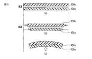
図5は、本実施形態における第1層109の原理を示している。 FIG. 5 shows the principle of the
図5(a)に示すように、第1層109における第1膜109aおよび第2膜109bは、高温(400℃)で形成される。このとき、第1膜109aおよび第2膜109bが同等の幅で形成された場合を考える。 As shown in FIG. 5A, the
その後、図5(b)に示すように、例えば第2層110の形成工程において、低温に設定される。このとき、図示するように、熱膨張係数の大きい第1膜109aは、熱膨張係数の小さい第2膜109bよりも幅の変化率が大きい。具体的には、第1膜109aのほうが、第2膜109bよりも小さくなる。 Thereafter, as shown in FIG. 5B, for example, in the step of forming the
図5(c)に示すように、実際は第1膜109aと第2膜109bとは接触している。このように、特性(ここでは、熱膨張係数)の異なる2層が接触している場合、これらにストレスが生じる。このとき、幅がより小さくなる第1膜109aを第2膜109bの内側(下部側)に形成することにより、外側(上部側)に向かってストレスが生じる。このストレスにより、上部側に膨らむ第1層109が形成される。 As shown in FIG. 5C, the
[効果]
上記第1の実施形態によれば、複数の貫通孔109cを有し、キャビティ130を形成する第1層109が第1膜109aと第2膜109bとの積層膜で構成されている。このとき、内側の第1膜109aの熱膨張係数は、外側の第2膜109bの熱膨張係数より大きい。このように熱膨張係数を制御することで、第1層109を上部側に膨らむ構造とすることができ、キャビティ130を大きくすることができる。これにより、第1層109と機能素子120との接触、および毛細管現象による封止膜(第2層110)のキャビティ130への侵入を防ぐことができ、信頼性の向上を図ることができる。[effect]
According to the first embodiment, the
<第2の実施形態>
図6を用いて第2の実施形態に係る電気部品について説明する。第1の実施形態では、第1層が熱膨張係数の異なる2膜で形成された。これに対し、第2の実施形態は、第1層が熱膨張係数の異なる3膜以上で形成される例である。なお、第2の実施形態において、第1の実施形態と同様の点については説明を省略し、異なる点について説明する。<Second Embodiment>
An electrical component according to the second embodiment will be described with reference to FIG. In the first embodiment, the first layer is formed of two films having different thermal expansion coefficients. In contrast, the second embodiment is an example in which the first layer is formed of three or more films having different thermal expansion coefficients. Note that in the second embodiment, description of the same points as in the first embodiment will be omitted, and different points will be described.
[構造]
図6は、第2の実施形態に係る電気部品の断面図を示している。[Construction]
FIG. 6 shows a cross-sectional view of an electrical component according to the second embodiment.
図6に示すように、本実施形態に係る電気部品は、機能素子120を有する基板100、第1層109、第2層110、および第3層111で構成されている。 As shown in FIG. 6, the electrical component according to this embodiment includes a
ここで、第2の実施形態において、第1の実施形態と異なる点は、第1層109が、内側(下部側)の第1膜109aと、第1膜109a上に形成された中側の第2膜109bと、第2膜109b上に形成された外側(上部側)の第3膜109dとの積層膜で構成されている点である。 Here, the second embodiment is different from the first embodiment in that the
より具体的には、第1膜109aの熱膨張係数は、第2膜109bおよび第3膜109dの熱膨張係数より大きい。第2膜109bの熱膨張係数は、第3膜109dの熱膨張係数より大きいことが望ましいが、小さくてもよい。すなわち、貫通孔109cを有する第1層109において、内側の熱膨張係数が最も大きくなる。 More specifically, the thermal expansion coefficient of the
ここで、第1膜109a、第2膜109bおよび第3膜109dはそれぞれ、例えばSiN膜またはSiO(SiO2)膜で構成される。この際、SiN膜またはSiO(SiO2)膜の成膜方法を制御することで、第1膜109aの熱膨張係数が最も大きくなるように制御される。このように、第1層109として、熱膨張係数の異なる3層を形成し、かつ内側の第1膜109aの熱膨張係数を最も大きくすることで、薄膜ドームが外側に膨らむように形成される。すなわち、キャビティ130内が大きく形成される。Here, the
また、第1層109は、3膜の積層膜に限らず、4膜以上の積層膜であってもよい。第1層109を4膜以上の積層膜とする構造の場合でも、内側の絶縁膜の熱膨張係数を最も大きくすることにより、目的を達成することができる。 Further, the
さらに、第1層109は、積層膜に限らず、内側から外側に向かって熱膨張係数が小さくなるようなグラデーション膜であってもよい。このとき、グラデーション膜として、SiN膜、またはSiO(SiO2)膜が形成され得るが、防湿性の観点からSiN膜が形成されることがより望ましい。Furthermore, the
[製造方法]
第2の実施形態における電気部品の製造工程においても、第1の実施形態と同様、図3(b)の工程まで行われる。すなわち、MEMS素子120および第1犠牲層105を覆うように、ポリイミド等の有機材料で構成される第2犠牲層108が塗布される。その後、第2犠牲層108が所望の形状にパターニングされる。[Production method]
In the electrical component manufacturing process according to the second embodiment, the process up to the process of FIG. 3B is performed as in the first embodiment. That is, the second
次に、第2犠牲層108を覆うように、複数の貫通孔109cを有する第1層109が形成される。 Next, a
より具体的には、まず、第2犠牲層108を覆うように、薄膜ドームの内側となる第1膜109aが形成される。第1膜109aは、膜厚が例えば数百nm〜数μmで形成される。第1膜109aの成膜方法としては、CVD法が用いられる。 More specifically, first, a
次に、第1膜109a上に、薄膜ドームの中側となる第2膜109bが形成される。第2膜109bは、膜厚が例えば数百nm〜数μmで形成される。この第2膜109bは、第1膜109aよりも熱膨張係数が小さくなるように制御される。第2膜109bの成膜方法としては、CVD法が用いられる。 Next, on the
次に、第2膜109b上に、薄膜ドームの外側となる第3膜109dが形成される。第3膜109dは、膜厚が例えば数百nm〜数μmで形成される。この第3膜109dは、第1膜109aよりも熱膨張係数が小さくなるように制御される。第3膜109dの成膜方法としては、CVD法が用いられる。 Next, a
次に、第3膜109d上に、図示せぬレジストが塗布される。その後、通常のリソグラフィ法で形成された図示せぬレジストパターンとRIE法またはウェットエッチング法により、薄膜ドームの内側膜(第1膜109a)、中間膜(第2膜109b)および外側膜(第3膜109d)に第1犠牲層105および第2犠牲層108除去用の複数の貫通孔109cが開口される。 Next, a resist (not shown) is applied on the
このようにして、熱膨張係数が大きい内側の第1膜109aと、それより熱膨張係数が小さい中側の第2膜109bおよび外側の第3膜109dとで構成され、複数の貫通孔109cを有する第1層109が形成される。 In this way, the inner
その後の工程は、第1の実施形態と同様の工程であるため、説明は省略する。 Subsequent steps are the same as those in the first embodiment, and a description thereof will be omitted.
[効果]
上記第2の実施形態によれば、第1の実施形態と同様の効果を得ることができる。[effect]
According to the second embodiment, the same effect as in the first embodiment can be obtained.
さらに、本実施形態では、貫通孔109cを有し、キャビティ130を形成する第1層109が3層以上の積層膜で構成されている。これにより、第1層109が2層で形成される第1の実施形態と比較して、第1層109の耐久性が強くなるとともに、大気中の水分の浸透を抑制することができる。 Further, in the present embodiment, the
その他、本発明は、上記各実施形態に限定されるものではなく、実施段階ではその要旨を逸脱しない範囲で、種々に変形することが可能である。さらに、上記実施形態には種々の段階の発明が含まれており、開示される複数の構成要件における適宜な組み合わせにより種々の発明が抽出され得る。例えば、実施形態に示される全構成要件から幾つかの構成要件が削除されても、発明が解決しようとする課題の欄で述べた課題が解決でき、発明の効果の欄で述べられている効果が得られる場合には、この構成要件が削除された構成が発明として抽出され得る。 In addition, the present invention is not limited to the above-described embodiments, and various modifications can be made without departing from the scope of the invention when it is practiced. Furthermore, the above embodiments include inventions at various stages, and various inventions can be extracted by appropriately combining a plurality of disclosed constituent elements. For example, even if some constituent requirements are deleted from all the constituent requirements shown in the embodiment, the problem described in the column of the problem to be solved by the invention can be solved, and the effect described in the column of the effect of the invention Can be obtained as an invention.
100…基板、109…第1層、109a…第1膜、109b…第2膜、109c…貫通孔、110…第2層、120…機能素子、130…キャビティ。 DESCRIPTION OF
Claims (5)
Translated fromJapanese前記基板上に形成された機能素子と、
前記基板上において前記機能素子を収納するキャビティを形成し、複数の貫通孔を有する第1層と、
前記第1層上に形成され、複数の前記貫通孔を塞ぐ第2層と、
を具備し、
前記第1層は、下部側に形成された第1膜と、前記第1膜上に形成され、前記第1膜より熱膨張係数が小さい第2膜と、を含むことを特徴とする電気部品。A substrate,
A functional element formed on the substrate;
Forming a cavity for housing the functional element on the substrate, and a first layer having a plurality of through holes;
A second layer formed on the first layer and closing the plurality of through holes;
Comprising
The first component includes: a first film formed on a lower side; and a second film formed on the first film and having a thermal expansion coefficient smaller than that of the first film. .
前記機能素子を覆うように、犠牲層を形成し、
前記犠牲層上に、下部側に形成された第1膜と、前記第1膜上に形成され、前記第1膜より熱膨張係数が小さい第2膜と、を含む第1層を第1温度で形成し、
前記第1層に、複数の貫通孔を開口し、
複数の前記貫通孔を通して前記犠牲層を除去して、前記基板上において前記機能素子を収納するキャビティを形成し、
前記第1層上に、複数の前記貫通孔を塞ぐ第2層を前記第1温度以下の第2温度で形成する
ことを特徴とする電気部品の製造方法。A functional element is formed on the substrate,
Forming a sacrificial layer so as to cover the functional element;
A first layer including a first film formed on the lower side on the sacrificial layer and a second film formed on the first film and having a smaller thermal expansion coefficient than the first film is formed as a first temperature. Formed with
Opening a plurality of through holes in the first layer;
Removing the sacrificial layer through the plurality of through holes to form a cavity for accommodating the functional element on the substrate;
On the first layer, a second layer that closes the plurality of through holes is formed at a second temperature equal to or lower than the first temperature.
前記第1膜および前記第2膜の熱膨張係数は、前記CVD法の条件によって制御されることを特徴とする請求項4に記載の電気部品の製造方法。The first film and the second film are formed by a CVD method,
5. The method of manufacturing an electrical component according to claim 4, wherein thermal expansion coefficients of the first film and the second film are controlled by conditions of the CVD method.
Priority Applications (2)
| Application Number | Priority Date | Filing Date | Title |
|---|---|---|---|
| JP2010188664AJP5204171B2 (en) | 2010-08-25 | 2010-08-25 | Electrical component and manufacturing method thereof |
| US13/215,457US8921997B2 (en) | 2010-08-25 | 2011-08-23 | Electrical component and method of manufacturing the same |
Applications Claiming Priority (1)
| Application Number | Priority Date | Filing Date | Title |
|---|---|---|---|
| JP2010188664AJP5204171B2 (en) | 2010-08-25 | 2010-08-25 | Electrical component and manufacturing method thereof |
Publications (2)
| Publication Number | Publication Date |
|---|---|
| JP2012045656A JP2012045656A (en) | 2012-03-08 |
| JP5204171B2true JP5204171B2 (en) | 2013-06-05 |
Family
ID=45696058
Family Applications (1)
| Application Number | Title | Priority Date | Filing Date |
|---|---|---|---|
| JP2010188664AExpired - Fee RelatedJP5204171B2 (en) | 2010-08-25 | 2010-08-25 | Electrical component and manufacturing method thereof |
Country Status (2)
| Country | Link |
|---|---|
| US (1) | US8921997B2 (en) |
| JP (1) | JP5204171B2 (en) |
Families Citing this family (23)
| Publication number | Priority date | Publication date | Assignee | Title |
|---|---|---|---|---|
| FR2980643A1 (en)* | 2011-09-28 | 2013-03-29 | St Microelectronics Grenoble 2 | OPTICAL ELECTRONIC HOUSING |
| US9165723B2 (en) | 2012-08-23 | 2015-10-20 | Harris Corporation | Switches for use in microelectromechanical and other systems, and processes for making same |
| US9053873B2 (en) | 2012-09-20 | 2015-06-09 | Harris Corporation | Switches for use in microelectromechanical and other systems, and processes for making same |
| US9053874B2 (en)* | 2012-09-20 | 2015-06-09 | Harris Corporation | MEMS switches and other miniaturized devices having encapsulating enclosures, and processes for fabricating same |
| JP2014155980A (en)* | 2013-02-15 | 2014-08-28 | Toshiba Corp | Electric component and method for producing the same |
| DE102013102213B4 (en)* | 2013-03-06 | 2020-01-02 | Snaptrack, Inc. | Miniaturized device with thin-film cover and method of manufacture |
| JP2014184513A (en)* | 2013-03-22 | 2014-10-02 | Toshiba Corp | Electric component and method for producing the same |
| JP2014200857A (en) | 2013-04-01 | 2014-10-27 | 株式会社東芝 | Mems device and manufacturing method of the same |
| JP2015112703A (en)* | 2013-12-13 | 2015-06-22 | 株式会社東芝 | MEMS device and manufacturing method thereof |
| JP2015174150A (en)* | 2014-03-13 | 2015-10-05 | 株式会社東芝 | Mems device and manufacturing method thereof |
| JP6331552B2 (en)* | 2014-03-25 | 2018-05-30 | セイコーエプソン株式会社 | MEMS device and manufacturing method thereof |
| JP2015223689A (en)* | 2014-05-30 | 2015-12-14 | 株式会社東芝 | Electronic component and manufacturing method of the same |
| DE102014112672B4 (en)* | 2014-09-03 | 2018-05-09 | Snaptrack, Inc. | Cover for a component and method for producing a cover for a component |
| JP2016102737A (en)* | 2014-11-28 | 2016-06-02 | セイコーエプソン株式会社 | Electronic device, physical quantity sensor, pressure sensor, vibrator, altimeter, electronic apparatus and mobile body |
| JP2016163917A (en)* | 2015-03-06 | 2016-09-08 | 株式会社東芝 | MEMS equipment |
| JP2016172291A (en)* | 2015-03-16 | 2016-09-29 | 株式会社東芝 | Electronic equipment, and manufacturing method of electronic equipment |
| US9975757B2 (en)* | 2015-06-03 | 2018-05-22 | Taiwan Semiconductor Manufacturing Co., Ltd. | Wafer Level Hermetic Seal Process for microelectromechanical systems (MEMS) devices |
| JP2017033985A (en) | 2015-07-29 | 2017-02-09 | セイコーエプソン株式会社 | Electronic device and manufacturing method of the same, oscillator, electronic device, and mobile body |
| US10574202B2 (en) | 2016-04-01 | 2020-02-25 | Skyworks Filter Solutions Japan Co., Ltd. | Electronic package including cavity formed by removal of sacrificial material from within a cap |
| DE102017125140B4 (en)* | 2017-10-26 | 2021-06-10 | Infineon Technologies Ag | Method for producing a hermetically sealed housing with a semiconductor component |
| DE102019120846B3 (en)* | 2019-08-01 | 2020-12-10 | RF360 Europe GmbH | Electrical component having a cavity and a method of making an electrical component having a cavity |
| US11365117B2 (en) | 2019-12-23 | 2022-06-21 | Industrial Technology Research Institute | MEMS device and manufacturing method of the same |
| US11939212B2 (en) | 2019-12-23 | 2024-03-26 | Industrial Technology Research Institute | MEMS device, manufacturing method of the same, and integrated MEMS module using the same |
Family Cites Families (20)
| Publication number | Priority date | Publication date | Assignee | Title |
|---|---|---|---|---|
| US6156623A (en)* | 1998-03-03 | 2000-12-05 | Advanced Technology Materials, Inc. | Stress control of thin films by mechanical deformation of wafer substrate |
| EP1108677B1 (en)* | 1999-12-15 | 2006-09-27 | Asulab S.A. | Method of hermetic In Situ encapsulation of microsystems |
| US7008812B1 (en) | 2000-05-30 | 2006-03-07 | Ic Mechanics, Inc. | Manufacture of MEMS structures in sealed cavity using dry-release MEMS device encapsulation |
| FR2864340B1 (en)* | 2003-12-19 | 2006-03-24 | Commissariat Energie Atomique | MICRO COMPONENT COMPRISING A HERMETIC MICROCAVITY AND METHOD OF MANUFACTURING SUCH MICROCOMPONENT |
| US7381583B1 (en) | 2004-05-24 | 2008-06-03 | The United States Of America As Represented By The Secretary Of The Air Force | MEMS RF switch integrated process |
| US7405924B2 (en)* | 2004-09-27 | 2008-07-29 | Idc, Llc | System and method for protecting microelectromechanical systems array using structurally reinforced back-plate |
| US7190039B2 (en)* | 2005-02-18 | 2007-03-13 | Micron Technology, Inc. | Microelectronic imagers with shaped image sensors and methods for manufacturing microelectronic imagers |
| US8043880B2 (en)* | 2005-07-28 | 2011-10-25 | Hewlett-Packard Development, L.P. | Microelectronic device |
| US7417307B2 (en)* | 2005-07-29 | 2008-08-26 | Hewlett-Packard Development Company, L.P. | System and method for direct-bonding of substrates |
| FR2911865B1 (en)* | 2007-01-26 | 2009-04-17 | Commissariat Energie Atomique | METHOD FOR PRODUCING A COMPONENT PROTECTION COVER ON A SUBSTRATE |
| US7923790B1 (en)* | 2007-03-09 | 2011-04-12 | Silicon Laboratories Inc. | Planar microshells for vacuum encapsulated devices and damascene method of manufacture |
| WO2009014118A1 (en)* | 2007-07-24 | 2009-01-29 | Rohm Co., Ltd. | Mems sensor, and mems sensor manufacturing method |
| JP2009043537A (en)* | 2007-08-08 | 2009-02-26 | Toshiba Corp | MEMS switch and manufacturing method thereof |
| TW200938479A (en) | 2007-10-22 | 2009-09-16 | Toshiba Kk | Micromachine device and method of manufacturing the same |
| JP4581011B2 (en)* | 2008-01-25 | 2010-11-17 | 株式会社東芝 | Electrical parts and manufacturing method |
| JP2010030020A (en)* | 2008-07-31 | 2010-02-12 | Seiko Epson Corp | Electronic device |
| JP2010123679A (en)* | 2008-11-18 | 2010-06-03 | Toshiba Corp | Hollow seal and method of manufacturing hollow seal |
| US7998775B2 (en)* | 2009-02-09 | 2011-08-16 | Taiwan Semiconductor Manufacturing Company, Ltd. | Silicon undercut prevention in sacrificial oxide release process and resulting MEMS structures |
| JP4700114B2 (en)* | 2009-02-10 | 2011-06-15 | シャープ株式会社 | Semiconductor module |
| US8053284B2 (en)* | 2009-08-13 | 2011-11-08 | International Business Machines Corporation | Method and package for circuit chip packaging |
- 2010
- 2010-08-25JPJP2010188664Apatent/JP5204171B2/ennot_activeExpired - Fee Related
- 2011
- 2011-08-23USUS13/215,457patent/US8921997B2/ennot_activeExpired - Fee Related
Also Published As
| Publication number | Publication date |
|---|---|
| US8921997B2 (en) | 2014-12-30 |
| JP2012045656A (en) | 2012-03-08 |
| US20120049390A1 (en) | 2012-03-01 |
Similar Documents
| Publication | Publication Date | Title |
|---|---|---|
| JP5204171B2 (en) | Electrical component and manufacturing method thereof | |
| TWI385784B (en) | Electrical device built into semiconductor integrated circuit | |
| JP5813471B2 (en) | MEMS element | |
| JP6165730B2 (en) | MEMS device anchoring | |
| TWI512800B (en) | Electrical component and method of manufacturing the same | |
| US20100002895A1 (en) | Condenser microphone and mems device | |
| TWI506740B (en) | Electrical component and method of manufacturing the same | |
| US8796845B2 (en) | Electronic device covered by multiple layers and method for manufacturing electronic device | |
| JP2010082797A (en) | Micromachine device and method of manufacturing the same | |
| JP2007000994A (en) | Semiconductor device | |
| US20160257560A1 (en) | Mems device | |
| CN104627948A (en) | Micromechanical sensor device and corresponding manufacturing method | |
| US20150170997A1 (en) | Mems device and manufacturing method of the same | |
| JP5784513B2 (en) | MEMS device and manufacturing method thereof | |
| CN113086939A (en) | MEMS device, method of manufacturing the same, and integrated MEMS using the same | |
| JP4581485B2 (en) | Acceleration sensor and manufacturing method thereof | |
| JP6095308B2 (en) | Semiconductor device and manufacturing method thereof | |
| JP2016055395A (en) | MEMS device and manufacturing method thereof | |
| JP2008093812A (en) | MEMS / semiconductor composite circuit and MEMS element | |
| JP2010123679A (en) | Hollow seal and method of manufacturing hollow seal | |
| JP2010207987A (en) | Method of manufacturing micromachine device | |
| JP4857718B2 (en) | Micromachine mixed electronic circuit device and method for manufacturing micromachine mixed electronic circuit device | |
| JP4774902B2 (en) | Manufacturing method of MEMS element | |
| JP2006224219A (en) | Manufacturing method of MEMS element | |
| JP2008307686A (en) | MEMS / semiconductor composite circuit and MEMS element |
Legal Events
| Date | Code | Title | Description |
|---|---|---|---|
| A621 | Written request for application examination | Free format text:JAPANESE INTERMEDIATE CODE: A621 Effective date:20120809 | |
| A977 | Report on retrieval | Free format text:JAPANESE INTERMEDIATE CODE: A971007 Effective date:20130116 | |
| TRDD | Decision of grant or rejection written | ||
| A01 | Written decision to grant a patent or to grant a registration (utility model) | Free format text:JAPANESE INTERMEDIATE CODE: A01 Effective date:20130122 | |
| A61 | First payment of annual fees (during grant procedure) | Free format text:JAPANESE INTERMEDIATE CODE: A61 Effective date:20130214 | |
| FPAY | Renewal fee payment (event date is renewal date of database) | Free format text:PAYMENT UNTIL: 20160222 Year of fee payment:3 | |
| LAPS | Cancellation because of no payment of annual fees |