JP5198226B2 - Substrate mounting table and substrate processing apparatus - Google Patents
Substrate mounting table and substrate processing apparatusDownload PDFInfo
- Publication number
- JP5198226B2 JP5198226B2JP2008297280AJP2008297280AJP5198226B2JP 5198226 B2JP5198226 B2JP 5198226B2JP 2008297280 AJP2008297280 AJP 2008297280AJP 2008297280 AJP2008297280 AJP 2008297280AJP 5198226 B2JP5198226 B2JP 5198226B2
- Authority
- JP
- Japan
- Prior art keywords
- heat transfer
- mounting table
- substrate
- transfer gas
- space
- Prior art date
- Legal status (The legal status is an assumption and is not a legal conclusion. Google has not performed a legal analysis and makes no representation as to the accuracy of the status listed.)
- Expired - Fee Related
Links
Images


Classifications
- H—ELECTRICITY
- H01—ELECTRIC ELEMENTS
- H01J—ELECTRIC DISCHARGE TUBES OR DISCHARGE LAMPS
- H01J37/00—Discharge tubes with provision for introducing objects or material to be exposed to the discharge, e.g. for the purpose of examination or processing thereof
- H01J37/32—Gas-filled discharge tubes
- H01J37/32431—Constructional details of the reactor
- H—ELECTRICITY
- H01—ELECTRIC ELEMENTS
- H01L—SEMICONDUCTOR DEVICES NOT COVERED BY CLASS H10
- H01L21/00—Processes or apparatus adapted for the manufacture or treatment of semiconductor or solid state devices or of parts thereof
- H01L21/67—Apparatus specially adapted for handling semiconductor or electric solid state devices during manufacture or treatment thereof; Apparatus specially adapted for handling wafers during manufacture or treatment of semiconductor or electric solid state devices or components ; Apparatus not specifically provided for elsewhere
- H01L21/67005—Apparatus not specifically provided for elsewhere
- H01L21/67011—Apparatus for manufacture or treatment
- H01L21/67098—Apparatus for thermal treatment
- H01L21/67109—Apparatus for thermal treatment mainly by convection
- H—ELECTRICITY
- H01—ELECTRIC ELEMENTS
- H01J—ELECTRIC DISCHARGE TUBES OR DISCHARGE LAMPS
- H01J2237/00—Discharge tubes exposing object to beam, e.g. for analysis treatment, etching, imaging
- H01J2237/20—Positioning, supporting, modifying or maintaining the physical state of objects being observed or treated
- H01J2237/2001—Maintaining constant desired temperature
Landscapes
- Engineering & Computer Science (AREA)
- Physics & Mathematics (AREA)
- General Physics & Mathematics (AREA)
- Chemical & Material Sciences (AREA)
- Analytical Chemistry (AREA)
- Condensed Matter Physics & Semiconductors (AREA)
- Plasma & Fusion (AREA)
- Manufacturing & Machinery (AREA)
- Computer Hardware Design (AREA)
- Microelectronics & Electronic Packaging (AREA)
- Power Engineering (AREA)
- Drying Of Semiconductors (AREA)
- Container, Conveyance, Adherence, Positioning, Of Wafer (AREA)
Description
Translated fromJapanese本発明は、半導体ウエハ等の基板を載置する基板載置台、および基板載置台に載置された基板に対して例えばドライエッチングのような処理を施す基板処理装置に関する。 The present invention relates to a substrate mounting table on which a substrate such as a semiconductor wafer is mounted, and a substrate processing apparatus for performing a process such as dry etching on the substrate mounted on the substrate mounting table.
半導体デバイスの製造プロセスにおいては、被処理基板である半導体ウエハ(以下単にウエハと記す)に対して、ドライエッチングやスパッタリング、CVD(化学気相成長)等のプラズマ処理が多用されている。 2. Description of the Related Art In semiconductor device manufacturing processes, plasma processing such as dry etching, sputtering, and CVD (chemical vapor deposition) is frequently used for semiconductor wafers (hereinafter simply referred to as wafers) that are substrates to be processed.
例えば、プラズマエッチング処理においては、チャンバ内にウエハを載置する載置台を設け、この載置台の上部を構成する静電チャックによりウエハを静電吸着して保持し、処理ガスのプラズマを形成してウエハに対してプラズマエッチング処理を施す。 For example, in a plasma etching process, a mounting table for mounting a wafer is provided in a chamber, and the wafer is electrostatically adsorbed and held by an electrostatic chuck constituting the upper portion of the mounting table to form plasma of a processing gas. A plasma etching process is performed on the wafer.
このような処理の際には、被処理基板であるウエハを所望の温度に制御する必要があり、そのために載置台内に冷媒流路を設けるとともに、ウエハが載置される載置台とウエハ裏面との間にHeガス等の熱伝達用ガスを導入してその圧力を変化させることによりウエハの温度制御を行ってエッチングレート等の処理レートを制御している。 In such processing, it is necessary to control the wafer, which is a substrate to be processed, to a desired temperature. For this purpose, a coolant channel is provided in the mounting table, and the mounting table on which the wafer is mounted and the wafer back surface. The temperature of the wafer is controlled by introducing a heat transfer gas such as He gas and changing the pressure between the two and the processing rate such as the etching rate.
しかしながら、近年、半導体デバイスの微細化が益々進んでおり、より高い精度でプラズマエッチング等のプラズマ処理を行うために、より高い精度でウエハの温度制御を行う必要がある。また、プラズマ処理装置のチャンバ内のウエハレスドライクリーニングを行う場合には、デポの付着を防ぐため、冷媒による冷却よりも、むしろより高い温度にすることが望まれる。 However, in recent years, semiconductor devices have been increasingly miniaturized, and in order to perform plasma processing such as plasma etching with higher accuracy, it is necessary to control the temperature of the wafer with higher accuracy. In addition, when performing waferless dry cleaning in the chamber of the plasma processing apparatus, it is desirable to set the temperature higher than cooling with a refrigerant in order to prevent deposition of deposits.
このような要請に対応可能な技術として、例えば特許文献1に記載されたものを挙げることができる。この技術は、載置台(吸着装置)の静電チャックとして構成される保持部材と冷媒流路との間に、ガス封入、排出を行うことができる伝熱ガス室を設け、伝熱をコントロールしてウエハの温度制御を行うものである。
しかしながら、上記特許文献1の技術を用いた場合には、伝熱ガス室という空洞部を設けるため、載置台の加工時に平面出しが困難となることや、真空時の圧力差による撓みにより、載置されたウエハとの接触が不十分となってかえって温度制御性が低下するおそれがある。さらに、空洞部を設けてそこにガスを導入しても、固体よりは断熱的となり、最近の高パワープロセスに対して十分な冷却ができないので、空洞部のみ温度が上がり、特異点となってしまいやすい。また、熱源となるプラズマの影響を受けやすい。これらの原因により、ウエハ面内温度のばらつきが生じるとエッチングレートが不均一になるため、ウエハ面内温度均一性が求められるが、特許文献1の技術ではそのような温度均一性制御を行うことが困難である。さらに、冷媒で冷却されている載置台の露出している部分は処理ガスによりデポが付着しやすい状態となっているため、その部分に局部的にデポが付着することがあるが、特許文献1の技術では、このような局部的なデポの付着を防止することは困難である。 However, when the technique of
本発明はかかる事情に鑑みてなされたものであって、基板との接触が良好で基板の温度を高精度で所望の温度に制御することができる基板載置台およびそれを用いた基板処理装置を提供することを目的とする。
また、基板面内の温度均一性を高めることができ、載置台への局部的なデポの付着を防止することができる基板載置台および基板処理装置を提供することを目的とする。The present invention has been made in view of such circumstances, and a substrate mounting table capable of controlling the temperature of the substrate to a desired temperature with high accuracy and a substrate processing apparatus using the same, which are in good contact with the substrate. The purpose is to provide.
It is another object of the present invention to provide a substrate mounting table and a substrate processing apparatus that can improve temperature uniformity within the substrate surface and can prevent local deposits on the mounting table.
上記課題を解決するため、本発明の第1の観点では、基板処理装置において基板を載置する基板載置台であって、載置台本体と、前記載置台本体の上部に設けられた、基板を載置する載置面を有する載置部と、冷熱または熱を前記載置台本体の上部に伝熱させるための熱源と、前記載置台本体の伝熱経路中に位置し、載置された基板に対応するように設けられた空間部、および前記空間部に充填された、多数の連通する空隙が存在する固体部材を有し、前記空間部に伝熱ガスを供給または前記空間部から伝熱ガスを排出することにより、前記熱源からの伝熱をコントロールする伝熱コントロール部と、前記空間部へ伝熱ガスを供給する伝熱ガス供給機構と、前記空間部から伝熱ガスを排出する伝熱ガス排出機構と、前記伝熱ガス供給機構による前記空間部への伝熱ガスの供給、前記伝熱ガス排出機構による前記空間部からの伝熱ガスの排出を制御する制御部とを具備し、前記固体部材は断熱材であることを特徴とする基板載置台を提供する。In order to solve the above problems, according to a first aspect of the present invention, there is provided a substrate mounting table on which a substrate is mounted in a substrate processing apparatus, the mounting table main body, and a substrate provided on an upper portion of the mounting table main body described above. A placement part having a placement surface to be placed, a heat source for transferring cold heat or heat to the upper part of the mounting table main body, and a substrate placed and placed in the heat transfer path of the mounting table main body And a solid member filled with the space and having a large number of communicating gaps, supplying heat transfer gas to the space or transferring heat from the space By discharging gas, a heat transfer control unit that controls heat transfer from the heat source, a heat transfer gas supply mechanism that supplies heat transfer gas to the space, and a heat transfer gas that discharges heat transfer gas from the space The hot gas discharge mechanism and the heat transfer gas supply mechanism And wherein the supply of the heat transfer gas into the space,and a control unit for controlling the discharge of the heat transfer gas from the space by the heat transfer gas dischargemechanism, wherein the solid member is a heat insulating material A substrate mounting table is provided.
上記第1の観点において、前記熱源は、載置台本体内に設けられた、冷媒が通流される冷媒流路を有するものとすることができる。In the first aspect, the heat source is provided in the mounting table body, refrigerantRu can be made to have a passing flows coolantchannel.
上記第1の観点において、前記空間部は基板の面内方向に沿って複数の副空間部に分割されており、前記伝熱ガス供給機構および前記伝熱ガス排出機構は、各副空間部に対して個別的に伝熱ガスの供給および排出を行うように構成することができる。この場合に、前記副空間部は同心状に形成することができる。また、隣接する前記副空間部の間は、前記固体部材と同種の緻密質部材からなる分離部材で分離されていることが好ましい。さらに、前記制御部は、各副空間部の伝熱ガスの圧力を個別的に制御するようにしてもよいし、前記各副空間部へ異なる種類の伝熱ガスを供給するように制御するようにしてもよい。さらにまた、前記各副空間部へ充填される固体部材の空隙率または材質を異ならせることもできる。 In the first aspect, the space portion is divided into a plurality of subspace portions along the in-plane direction of the substrate, and the heat transfer gas supply mechanism and the heat transfer gas discharge mechanism are provided in each subspace portion. On the other hand, the heat transfer gas can be individually supplied and discharged. In this case, the subspace portion can be formed concentrically. Moreover, it is preferable to isolate | separate between the said subspace parts by the separation member which consists of a dense member of the same kind as the said solid member. Further, the control unit may individually control the pressure of the heat transfer gas in each sub space portion, or may control to supply different types of heat transfer gas to each sub space portion. It may be. Furthermore, the porosity or material of the solid member filled in each of the subspaces can be varied.
本発明の第2の観点では、基板処理装置において基板を載置する基板載置台であって、載置台本体と、前記載置台本体の上部に設けられた、基板を載置する載置面を有する載置部と、冷熱または熱を前記載置台本体の上部に伝熱させるための熱源と、前記載置台本体の伝熱経路中に位置し、載置された基板に対応するように設けられた空間部、および前記空間部に充填された、多数の連通する空隙が存在する固体部材を有し、前記空間部に伝熱ガスを供給または前記空間部から伝熱ガスを排出することにより、前記熱源からの伝熱をコントロールする伝熱コントロール部と、前記空間部へ伝熱ガスを供給する伝熱ガス供給機構と、前記空間部から伝熱ガスを排出する伝熱ガス排出機構と、前記伝熱ガス供給機構による前記空間部への伝熱ガスの供給、前記伝熱ガス排出機構による前記空間部からの伝熱ガスの排出を制御する制御部とを具備し、前記空間部に充填される前記固体部材は、基板の面内方向に沿って空隙率に分布が生じていることを特徴とする基板載置台を提供する。
上記第2の観点において、前記空間部に充填される前記固体部材は、基板の面内方向に沿って空隙率の異なる複数の部位を有するように構成することができる。また、前記空間部に充填される前記固体部材は、基板の面内方向に沿って空隙率にグラデーションを有するように構成することができる。According to a second aspect of the present invention, there is provided a substrate mounting table on which a substrate is mounted in a substrate processing apparatus, the mounting table main body, and a mounting surface on which the substrate is mounted provided above the mounting table main body. A mounting unit, a heat source for transferring cold or heat to the upper part of the mounting table main body, and a heat transfer path of the mounting table main body, provided to correspond to the mounted substrate A solid member having a large number of communicating voids filled in the space portion and supplying the heat transfer gas to the space portion or discharging the heat transfer gas from the space portion, A heat transfer control unit that controls heat transfer from the heat source, a heat transfer gas supply mechanism that supplies heat transfer gas to the space, a heat transfer gas discharge mechanism that discharges heat transfer gas from the space, and Heat transfer gas to the space by the heat transfer gas supply mechanism A controller that controls supply and discharge of the heat transfer gas from the space by the heat transfer gas discharge mechanism, and the solid member filled in the space is a gap along the in-plane direction of the substrate Provided is a substrate mounting table characterized by having a distribution in rate.
In the second aspect, the solid member filled in the space portion can be configured to have a plurality of portions having different porosity along the in-plane direction of the substrate. Further, the solid member filled in the space portion can be configured to have gradation in the porosity along the in-plane direction of the substrate.
上記第1および第2の観点において、前記空間部は、その高さが100μm以下の微小空間であることが、制御性の点から好ましい。また、前記載置部は、基板を静電吸着する静電チャックを有するものとすることができる。また、前記載置部の載置面に載置された基板の裏面側に伝熱ガスを供給する伝熱ガス供給機構をさらに具備することが好ましい。In the first and second aspects, the space is preferably a minute space having a height of 100 μm or less from the viewpoint of controllability.Further, the placement unit may have an electrostatic chuck that electrostatically attracts the substrate. Moreover, it is preferable to further comprise a heat transfer gas supply mechanism for supplying a heat transfer gas to the back surface side of the substrate placed on the placement surface of the placement portion.
本発明の第3の観点では、基板処理装置において基板を載置する基板載置台であって、載置台本体と、前記載置台本体の上部に設けられた、基板を載置する載置面を有する載置部と、前記載置台本体内で異なる温度に保持され、冷熱または熱を前記載置台本体の上部に伝熱させる複数の熱源と、前記載置台本体の前記複数の熱源の間に設けられた空間部、および前記空間部に充填された、多数の連通する空隙が存在する固体部材を有し、前記空間部に伝熱ガスを供給または前記空間部から伝熱ガスを排出することにより、前記複数の熱源の間の伝熱をコントロールする伝熱コントロール部と、前記空間部へ伝熱ガスを供給する伝熱ガス供給機構と、前記空間部から伝熱ガスを排出する伝熱ガス排出機構と、前記伝熱ガス供給機構による前記空間部への伝熱ガスの供給、前記伝熱ガス排出機構による前記空間部からの伝熱ガスの排出を制御する制御部とを具備し、前記固体部材は断熱材であることを特徴とする基板載置台を提供する。 According to a third aspect of the present invention, there is provided a substrate mounting table on which a substrate is mounted in a substrate processing apparatus, the mounting table main body, and a mounting surface on which the substrate is mounted provided above the mounting table main body. A plurality of heat sources that are held at different temperatures in the mounting table main body and transfer cold or heat to the top of the mounting table main body, and the plurality of heat sources of the mounting table main body. And a solid member filled with the space portion and having a large number of communicating voids, and supplying the heat transfer gas to the space portion or discharging the heat transfer gas from the space portion A heat transfer control unit that controls heat transfer between the plurality of heat sources, a heat transfer gas supply mechanism that supplies a heat transfer gas to the space, and a heat transfer gas discharge that discharges the heat transfer gas from the space Mechanism and the empty space by the heat transfer gas supply mechanism. And a controller that controls supply of heat transfer gas to the unit and discharge of the heat transfer gas from the space by the heat transfer gas discharge mechanism, and the solid member is a heat insulating material. Provide a mounting table.
本発明の第4の観点では、基板処理装置において基板を載置する基板載置台であって、載置台本体と、前記載置台本体の上部に設けられた、基板を載置する載置面を有する載置部と、冷熱または熱を前記載置台本体の上部に伝熱させるための熱源と、前記載置台本体の伝熱経路中に位置し、載置された基板に対応するように設けられた空間部、および前記空間部に充填された、多数の連通する空隙が存在する固体部材を有し、前記空間部に伝熱ガスを供給または前記空間部から伝熱ガスを排出することにより、前記熱源からの伝熱をコントロールする伝熱コントロール部と、前記空間部へ伝熱ガスを供給する伝熱ガス供給機構と、前記空間部から伝熱ガスを排出する伝熱ガス排出機構とを具備し、前記固体部材は断熱材であることを特徴とする基板載置台を提供する。 According to a fourth aspect of the present invention, there is provided a substrate mounting table for mounting a substrate in the substrate processing apparatus, wherein the mounting table main body and a mounting surface for mounting the substrate provided on the upper part of the mounting table main body are provided. A mounting unit, a heat source for transferring cold or heat to the upper part of the mounting table main body, and a heat transfer path of the mounting table main body, provided to correspond to the mounted substrate A solid member having a large number of communicating voids filled in the space portion and supplying the heat transfer gas to the space portion or discharging the heat transfer gas from the space portion, A heat transfer control unit that controls heat transfer from the heat source, a heat transfer gas supply mechanism that supplies heat transfer gas to the space, and a heat transfer gas discharge mechanism that discharges heat transfer gas from the space The solid member is a heat insulating material. Providing a substrate mounting table.
上記第1、第3、第4の観点において、前記熱源は、前記載置台本体の外側および内側に、互いに温度の異なる冷媒が通流される外側冷媒循環路および内側冷媒循環路を有し、前記固体部材を有する前記空間部は、前記外側冷媒循環路および前記内側冷媒循環路の間に設けられている構成とすることができる。 In the first, third, and fourth aspects, the heat source has an outer refrigerant circulation path and an inner refrigerant circulation path through which refrigerants having different temperatures flow, on the outer side and the inner side of the mounting table main body, The space portion having a solid member may be provided between the outer refrigerant circulation path and the inner refrigerant circulation path.
本発明の第5の観点では、基板を収容し、内部が減圧保持される処理容器と、 In a fifth aspect of the present invention, a processing container that accommodates a substrate and holds the inside under reduced pressure;
前記処理容器内に設けられ、基板が載置され、第1の観点から第4の観点のいずれかの構成を有する基板載置台と、前記処理室内で基板に所定の処理を施す処理機構とを具備することを特徴とする基板処理装置を提供する。 A substrate mounting table provided in the processing container, on which a substrate is mounted, and having a configuration according to any one of the first to fourth aspects; and a processing mechanism for performing a predetermined process on the substrate in the processing chamber. Provided is a substrate processing apparatus.
上記第5の観点において、前記処理機構は、プラズマ生成機構を有し、それにより生成されたプラズマにより基板に対してプラズマ処理を施すものとすることができる。 In the fifth aspect, the processing mechanism may have a plasma generation mechanism, and the substrate may be subjected to plasma processing by plasma generated thereby.
本発明によれば、載置台本体の伝熱経路中に位置し、載置された基板に対応するように設けられた空間部、および空間部に充填された、多数の連通する空隙が存在する固体部材を有する伝熱コントロール部を設け、空間部に伝熱ガスを供給または空間部から伝熱ガスを排出することにより、熱源からの伝熱をコントロールするので、空間のみ設けた場合のように、加工時の平面出しの困難性や、真空時の撓み等の問題が生じず、基板との接触が良好に維持することができ、基板の温度を高精度で所望の温度に応答性よく制御することができる。また、空間部は高圧力状態(例えば1atm)から真空状態まで広い範囲の圧力にすることができるので、熱伝達性を広い範囲でコントロールすることができ、広い温度範囲で温度制御することができる。 According to the present invention, there is a space portion that is located in the heat transfer path of the mounting table main body and is provided so as to correspond to the mounted substrate, and a large number of communicating gaps that are filled in the space portion. By providing a heat transfer control unit with a solid member and controlling the heat transfer from the heat source by supplying the heat transfer gas to the space or discharging the heat transfer gas from the space, as in the case where only the space is provided・ There is no difficulty in flattening during processing, no problems such as bending during vacuum, etc., and good contact with the substrate can be maintained, and the temperature of the substrate can be controlled with high accuracy and responsiveness to the desired temperature. can do. Moreover, since the space can be in a wide range of pressure from a high pressure state (for example, 1 atm) to a vacuum state, the heat transferability can be controlled in a wide range, and the temperature can be controlled in a wide temperature range. .
また、空間部を基板の面内方向に沿って複数の副空間部に分割された構造にし、伝熱ガス供給機構および伝熱ガス排出機構が、各副空間部に対して個別的に伝熱ガスの供給および排出を行うように構成することにより、副空間部毎に伝熱をコントロールすることができ、基板の温度分布を均一にすることができる。また、積極的に温度分布を持たせたい場合にも、副空間部の伝熱をコントロールすることにより所望の温度分布になるようにすることができ、例えば、局部的なデポの発生を防止することができる。 In addition, the space portion is divided into a plurality of subspace portions along the in-plane direction of the substrate, and the heat transfer gas supply mechanism and the heat transfer gas discharge mechanism individually transfer heat to each subspace portion. By configuring so as to supply and discharge the gas, heat transfer can be controlled for each subspace, and the temperature distribution of the substrate can be made uniform. In addition, when it is desired to have a positive temperature distribution, it is possible to achieve a desired temperature distribution by controlling the heat transfer in the subspace, for example, preventing the occurrence of local depots. be able to.
さらに、固体部材を、基板の面内方向に沿って空隙率に分布が生じているものとすることにより、空隙率の分布に応じて伝熱の分布を生じさせることができ、それにより基板温度を均一にしたり、所望の温度分布を持たせたりすることができる。 Further, by providing the solid member with a distribution in the porosity along the in-plane direction of the substrate, a heat transfer distribution can be generated in accordance with the distribution of the porosity, whereby the substrate temperature Can be made uniform or have a desired temperature distribution.
さらにまた、前記載置台本体内で異なる温度に保持され、冷熱または熱を前記載置台本体の上部に伝熱させる複数の熱源を有し、基板に温度分布を持たせるような場合に、これら熱源の間に上記伝熱コントロール部を設けることにより、複数の熱源の間の温度勾配等を制御することができる。 Further, when the substrate has a plurality of heat sources that are kept at different temperatures in the mounting table main body and transfer cold heat or heat to the top of the mounting table main body, and the substrate has a temperature distribution, these heat sources By providing the heat transfer control unit between them, temperature gradients between a plurality of heat sources can be controlled.
以下、添附図面を参照して本発明の実施形態について説明する。
<第1の実施形態>
図1は本発明の第1の実施形態に係るウエハ載置台(基板載置台)が設けられたプラズマ処理装置を示す断面図である。Embodiments of the present invention will be described below with reference to the accompanying drawings.
<First Embodiment>
FIG. 1 is a cross-sectional view showing a plasma processing apparatus provided with a wafer mounting table (substrate mounting table) according to a first embodiment of the present invention.
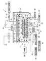
このプラズマ処理装置(基板処理装置)1は、電極板が上下平行に対向し、これらの間に形成された高周波電界により容量結合プラズマが形成される平行平板エッチング装置として構成されている。 The plasma processing apparatus (substrate processing apparatus) 1 is configured as a parallel plate etching apparatus in which electrode plates face each other in the vertical direction and capacitively coupled plasma is formed by a high frequency electric field formed therebetween.
このプラズマ処理装置1は、例えば表面が陽極酸化処理されたアルミニウムからなる円筒形状に成形されたチャンバ2を有している。チャンバ2内の底部にはセラミックなどの絶縁部材3を介して、被処理基板である半導体ウエハ(以下単に「ウエハ」と記す)Wを載置する本実施形態のウエハ載置台(基板載置台)4が設けられている。本実施形態においては、このウエハ載置台4は後述するように下部電極として機能する。 The
ウエハ載置台4の上方には、このウエハ載置台4と平行に対向して上部電極として機能するシャワーヘッド10が設けられている。このシャワーヘッド10は、ウエハ載置台4との対向面を構成するとともに多数の吐出孔12を有する電極板11と、この電極板11を支持し、導電性材料、例えば表面が陽極酸化処理されたアルミニウムからなる水冷構造の電極板支持体13とによって構成されている。電極板支持体13内にはガス拡散空間13aが形成されている。 Above the wafer mounting table 4, a
このシャワーヘッド10とチャンバ2の側壁の間にはリング状に絶縁材15が設けられている。この絶縁材15はチャンバ2の側壁に取り付けられている。また、絶縁材15の下端には、その周囲に沿って内側に延びる絶縁性の支持部材16が取り付けられており、シャワーヘッド10は、支持部材16により支持されている。なお、シャワーヘッド10とウエハ載置台4とは、例えば10〜60mm程度離間している。 An insulating
前記シャワーヘッド10における電極板支持体13にはガス拡散空間13aに至るガス導入口18が設けられ、このガス導入口18にはガス供給管19の一端が接続されており、ガス供給管19の他端は処理ガス供給源20に接続されている。そして、処理ガス供給源20からガス供給管19を介してエッチングのための処理ガスがシャワーヘッド10へ供給され、電極板支持体13のガス拡散空間13aを経て吐出孔12からウエハW上へ吐出されるようになっている。ガス供給管19には、バルブ21およびマスフローコントローラ22が設けられている。 The
エッチングのための処理ガスとしては、従来用いられている種々のものを採用することができ、例えばフロロカーボンガス(CxFy)やハイドロフロロカーボンガス(CpHqFr)のようなハロゲン元素を含有するガスを好適に用いることができる。他にAr、He等の希ガスやN2ガス、O2ガス等を添加してもよい。As a processing gas for etching, various conventionally used gases can be employed. For example, a halogen element such as a fluorocarbon gas (Cx Fy ) or a hydrofluorocarbon gas (Cp Hq Fr ). A gas containing can be suitably used. In addition, a rare gas such as Ar or He, N2 gas, O2 gas, or the like may be added.
チャンバ2の底部には排気管25が接続されており、この排気管25には排気装置26が接続されている。排気装置26はターボ分子ポンプなどの真空ポンプを備えており、これによりチャンバ2内を所定の減圧雰囲気、例えば1Pa以下の所定の圧力まで真空引き可能なように構成されている。排気管25には自動圧力制御弁(図示せず)が設けられており、これにより、チャンバ2内を所定の圧力に制御可能となっている。また、チャンバ2の側壁にはゲートバルブ27が設けられており、このゲートバルブ27を開にした状態でウエハWが隣接するロードロック室(図示せず)との間で搬送されるようになっている。 An
シャワーヘッド10には、整合器31を介して第1の高周波電源30が接続されており、その際の給電はシャワーヘッド10における電極板支持体13の上面中央部に接続された給電棒33により行われる。また、シャワーヘッド10にはローパスフィルタ(LPF)35が接続されている。この第1の高周波電源30から高周波電力が供給されることにより、ウエハWの上部電極であるシャワーヘッド10と下部電極であるウエハ載置台4との間に高周波電界が形成され、処理ガスのプラズマが生成される。この第1の高周波電源30は、例えば27MHz以上の周波数を有しており、具体例として60MHzが用いられる。このように比較的高い周波数を印加することによりチャンバ2内に好ましい解離状態でかつ高密度のプラズマを形成することができ、低圧条件下のプラズマ処理が可能となる。 A first high
本実施形態に係るウエハ載置台4は、略円柱状をなしており、絶縁部材3の上に設けられた金属製、例えばアルミニウム製の載置台本体41を有する。載置台本体41の上には、ウエハWの載置部として機能する、ウエハWの載置面を有する静電チャック42とを有している。静電チャック42は載置台本体41よりも小径であり、載置台本体41の上端周縁部には、静電チャック42を囲むように、環状のフォーカスリング43が配置されている。このフォーカスリング43は例えば絶縁材料からなっており、これによりエッチングの均一性が向上される。なお、載置台本体41は下部電極として機能する。 The wafer mounting table 4 according to the present embodiment has a substantially cylindrical shape, and includes a mounting
載置台本体41の内部には、冷媒循環路45が設けられており、この冷媒循環路45には、冷媒導入管46および冷媒排出管47が接続されている。この冷媒循環路45には、例えばフッ素不活性液体などの冷媒が冷媒供給機構48から冷媒導入管46を介して供給されて循環され、その冷熱がウエハWに伝達されるようになっている。冷媒温度は低い方が冷却能力が高く好ましいが、低すぎると結露を起こす。 A
静電チャック42は、ウエハWより若干小径に形成され、誘電体からなる本体42aとその中に介在された電極42bとを有している。電極42bには直流電源50が接続されており、この直流電源50から例えば1.5kVの直流電圧が印加されることにより、静電気力、例えばクーロン力、ジョンセン・ラーベック力によってその上に載置されたウエハWを静電吸着する。直流電源50はスイッチ51によりオン・オフされるようになっている。本体42aを構成する誘電体としてはAl2O3、Zr2O3、Si3N4、Y2O3等のセラミックスが例示される。The
ウエハ載置台4に載置されたウエハWの裏面側には、伝熱ガスであるHeガスを供給するためのガス流路52が接続されている。ガス流路52にはガス供給配管53が接続されており、ガス供給配管53にはHe供給機構55が接続されている。そしてHe供給機構55からガス供給配管53およびガス流路52を介してHeガスがウエハWの裏面に供給され、Heガスを介して冷媒の冷熱をウエハWに伝達するようになっている。すなわち、Heガスは冷媒の冷熱を伝達する伝熱ガスとして供給される。 A
載置台本体41の内部の冷媒循環路45と静電チャック42との間の伝熱経路には、伝熱コントロール部60が水平に設けられている。伝熱コントロール部60は、図2に示すように、載置台本体41内のウエハWに対応する位置に設けられた、ウエハWよりも大径の円板状をなす空間部61と、空間部61内に充填された、多数の連通する空隙が存在する固体部材62とで構成されている。 A heat
固体部材62は、空隙に伝熱ガスが存在しないときに断熱できるように断熱材で構成することが好ましい。また、安定でかつ容易に変形しないように硬度および機械的強度が比較的高い材料が好ましい。このような観点から固体部材62としては多孔質セラミックスが好適である。また、固体部材62としては、多孔質金属材料、発泡ゴム、グラスファイバー等も使用することができる。The
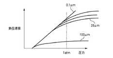
空間部61は、高さが小さいほうが制御性がよく、高さが100μm以下の微小空間であることが好ましい。図3に拡大して示すように、このような微小空間である空間部61は、微視的に見ると平坦性が悪いが、その高さは平均的な高さとして把握することができる。このようにして求めた種々の高さの微小空間におけるガスの圧力と熱伝導率の関係を図4に示す。この図に示すように、微小空間の高さが100μm以下で圧力に対する熱伝導率の変化が比較的大きく、制御性が高いことがわかる。 The
この伝熱コントロール部60の空間部61には、その中に伝熱ガスを供給する供給流路63が接続されている。また、この供給流路63には、供給配管64を介して伝熱ガス供給機構65が接続されている。また、空間部61には、空間部61内の伝熱ガスを排出する排出流路66が接続されている。この排出流路66には、排出配管67を介して伝熱ガス排出機構68が接続されている。A
伝熱ガス供給機構65は、伝熱コントロール部60の容器61内に伝熱ガスを供給する機能を有しており、固体部材62の空隙を所定の圧力の伝熱ガスで充填することにより、伝熱コントロール部60において伝熱ガスを介して熱伝達させる。このとき、伝熱ガスの圧力を制御することにより熱伝達性を制御することができる。一方、伝熱ガス排出機構68は、伝熱コントロール部60の容器61から伝熱ガスを排出する機能を有しており、固体部材62の空隙を真空状態として、伝熱コントロール部60の熱伝達性を低下させる。 The heat transfer
下部電極として機能するウエハ載置台4の載置台本体41には、給電線70aを介して第2の高周波電源70が接続されており、給電線70aには整合器71が介在されている。この第2の高周波電源70の周波数は、例えば100kHz〜13.56MHzの範囲であり、具体例として2MHzが用いられる。このような範囲の周波数を印加することにより、被処理体であるウエハWに対してダメージを与えることなく適切なイオン作用を与えることができる。なお、載置台本体41にはハイパスフィルタ72が接続されている。 A second high-
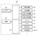
プラズマ処理装置1は制御部80を備えている。この制御部80は、図5のブロック図に示すように、コントローラ81と、ユーザーインターフェース82と、記憶部83とを有している。コントローラ81は、マイクロプロセッサ(コンピュータ)からなり、プラズマ処理装置1の各構成部、例えば冷媒供給機構48、He供給機構55、伝熱ガス供給機構65、伝熱ガス排出機構68、排気装置26、静電チャック42のための直流電源50のスイッチ51、バルブ21、マスフローコントローラ22等が制御される。ユーザーインターフェース82はコントローラ81に接続され、オペレータがプラズマ処理装置1を管理するためにコマンド等の入力操作を行うキーボードや、プラズマ処理装置1の稼働状況を可視化して表示するディスプレイ等からなる。記憶部83もコントローラ81に接続され、その中にプラズマ処理装置1の各構成部の制御対象を制御するための制御プログラムや、プラズマ処理装置1に所定の処理を行わせるためのプログラムすなわち処理レシピが格納されている。処理レシピは記憶部83の中の記憶媒体に記憶されている。記憶媒体は、ハードディスクのような固定的なものであってもよいし、CDROM、DVD、フラッシュメモリ等の可搬性のものであってもよい。また、他の装置から、例えば専用回線を介してレシピを適宜伝送させるようにしてもよい。そして、コントローラ81は、必要に応じて、ユーザーインターフェース82からの指示等にて任意の処理レシピを記憶部83から呼び出して実行させ、これによりプラズマ処理装置1では、コントローラ81の制御下で、所定の処理が行われる。 The
次に、以上のように構成されるプラズマ処理装置1における処理動作について説明する。
まず、被処理基板であるウエハWは、ゲートバルブ27が開放された後、図示しないロードロック室からチャンバ2内へと搬入され、ウエハ載置台4の静電チャック42上に載置される。次いで、ゲートバルブ27が閉じられ、排気装置26によって、チャンバ2内が所定の真空度まで真空引きされる。Next, the processing operation in the
First, after the
その後、バルブ21が開放されて、処理ガス供給源20から処理ガスがマスフローコントローラ22によってその流量が調整されつつ、ガス供給管19、ガス導入口18を通ってシャワーヘッド10の内部のガス拡散空間13aへ導入され、さらに電極板11の吐出孔12を通って、図1の矢印に示すように、ウエハWに対して均一に吐出され、チャンバ2内の圧力が所定の値に維持される。 Thereafter, the
その際に、第1の高周波電源30から27MHz以上、例えば60MHzの高周波が上部電極であるシャワーヘッド10に印加され、これにより、上部電極としてのシャワーヘッド10と下部電極としてのウエハ載置台4との間に高周波電界が生じ、処理ガスが解離してプラズマ化し、このプラズマにより、ウエハWに対してエッチング処理が施される。このようにしてプラズマが生成されると同時に、高圧直流電源50から静電チャック42の電極42bに直流電圧が印加されることによって、ウエハWが静電チャック11上に静電吸着される。 At that time, a high frequency of 27 MHz or more, for example, 60 MHz, is applied from the first high
他方、第2の高周波電源70からは、100kHz〜13.56MHz、例えば2MHzの高周波が下部電極であるウエハ載置台4に印加される。これにより、プラズマ中のイオンがウエハ載置台4側へ引き込まれ、イオンアシストによりエッチングの異方性が高められる。 On the other hand, a high frequency of 100 kHz to 13.56 MHz, for example, 2 MHz, is applied from the second high
このようなプラズマエッチングを複数のウエハWに対して繰り返し行い、所定枚数の処理が終了した時点で、チャンバ2内にウエハWを入れずに、チャンバ2内にプラズマを生成して、チャンバ2内のウエハレスドライクリーニングを行う。 Such plasma etching is repeatedly performed on a plurality of wafers W, and when a predetermined number of processes are completed, plasma is generated in the
以上のような、プラズマエッチングにおいては、高精度でエッチングを行うために、ウエハWの温度を制御する必要があり、そのため冷媒循環路45に冷媒を流しつつ、ウエハWの裏面側に熱伝達用ガスであるHeガスを供給し、冷媒の冷熱をウエハWに伝達してウエハWの温度を制御する。 In the plasma etching as described above, it is necessary to control the temperature of the wafer W in order to perform etching with high accuracy. For this reason, the heat is transferred to the back side of the wafer W while flowing the coolant through the
しかしながら、このような温度制御のみでは、温度調整マージンが小さく所望の精密な温度制御には不十分である。また、ウエハレスドライクリーニング時には、ウエハ載置台4の温度をプロセス時の温度より高くしてデポを除去しやすい状態にする必要があるが、上記手法では、このような温度に対応することが困難である。 However, such temperature control alone is not sufficient for a desired precise temperature control with a small temperature adjustment margin. Further, at the time of waferless dry cleaning, it is necessary to make the temperature of the wafer mounting table 4 higher than the temperature at the time of processing so that the deposit can be easily removed. However, it is difficult to cope with such a temperature with the above method. It is.
そこで、本実施形態では、ウエハ載置台4の載置台本体41の内部に、伝熱コントロール部60を設けている。伝熱コントロール部60は、載置台本体41内に設けられた空間部61内に多孔質セラミックス等の多数の連通する空隙が存在する固体部材62を有しており、伝熱ガス供給機構65により空間部61へ伝熱ガスを供給することにより空隙に伝熱ガスを存在させて熱伝達させることができ、また、その際の伝熱ガスの圧力を制御することにより、熱伝達性を制御することができる。また、伝熱ガス排出機構68により伝熱ガスを排出することにより固体部材62の空隙を真空状態として熱伝達性を低下させることができる。さらに、伝熱ガス供給機構65により伝熱ガスを空間部61に供給しつつ、伝熱ガス排出機構68により空間部61から伝熱ガスを排出して伝熱ガスを循環させることにより、冷却を促進することもできる。このように、伝熱コントロール部60に対する伝熱ガスの供給・排出および伝熱ガスの圧力制御を行うことができ、さらに伝熱ガスを循環させて冷却を促進することができるので、ウエハWの温度制御性および応答性を高くすることができる。また、空間部61は高圧力状態から真空状態まで広い範囲の圧力にすることができるので、熱伝達性を広い範囲でコントロールすることができ、ウエハ載置台4、ひいてはウエハWを広い温度範囲で温度制御することができる。例えば、チャンバ2内のウエハレスドライクリーニングを行う場合に、固体部材62の空隙を真空状態として断熱し、ウエハ載置台4の温度を高くしてデポの除去を促進することもできる。 Therefore, in the present embodiment, the heat
また、伝熱コントロール部60が単なる空間の場合には、載置台の加工時に平面出しが困難となることや、真空時の圧力差による撓みにより、載置されたウエハとの接触が不十分となってかえって温度制御性が低下するおそれがあるが、このように空間部61内に連通する空隙を有する固体部材62を充填させるので、このような不都合は生じない。また、固体部材62の空隙に伝熱ガスを充填させればよいので、空間全部に伝熱ガスを充填させる場合に比べて伝熱ガスの量を少なくすることができる。 In addition, when the heat
<第2の実施形態>
次に、本発明の第2の実施形態に係るウエハ載置台(基板載置台)について説明する。図6は、本発明の第2の実施形態に係るウエハ載置台を示す断面図である。本実施形態に係るウエハ載置台4′は、内部の冷媒循環路45と静電チャック42との間に伝熱コントロール部60′が水平に設けられている。伝熱コントロール部60′は、載置台本体41内のウエハWに対応する位置に設けられた、ウエハWよりも大径の円板状をなす空間部61′を有しており、その中は円環状の分離部材61cにより副空間部として、中央空間部61aと外側空間部61bとに同心円状に分離されている。そして、これら中央空間部61aと外側空間部61bに、それぞれ固体部材62a,62bが充填されている。固体部材62a,62bは上記固体部材62と同様、多数の連通する空隙が存在するものであり、典型例として多孔質セラミックスを挙げることができる。<Second Embodiment>
Next, a wafer mounting table (substrate mounting table) according to a second embodiment of the present invention will be described. FIG. 6 is a sectional view showing a wafer mounting table according to the second embodiment of the present invention. In the wafer mounting table 4 ′ according to this embodiment, a heat
そして、中央空間部61aには、その中に伝熱ガスを供給する供給流路63aおよびその中から伝熱ガスを排出する排出流路66aが設けられており、これらはそれぞれ供給配管64aおよび排出配管67aを介して図示しない伝熱ガス供給機構および伝熱ガス排出機構に接続されている。また、外側空間部61bには、その中に伝熱ガスを供給する供給流路63bおよびその中から伝熱ガスを排出する排出流路66bが設けられており、これらはそれぞれ供給配管64bおよび排出配管67bを介して図示しない上記伝熱ガス供給機構および伝熱ガス排出機構に接続されている。 The
このように伝熱コントロール部60′では、空間部61′を中央空間部61aと外側空間部61bとに分け、これらに独立に伝熱ガスの供給および排出を行うようにしたので、中央空間部61aと外側空間部61bに供給する伝熱ガスの圧力を異ならせたり、これらに異なる種類の伝熱ガスを供給することにより、伝熱コントロール部60′の中央部分と外側部分とで伝熱を異ならせて別個に温度制御を行うことができる。 As described above, in the heat
例えば、ウエハWの温度の面内均一性が不十分であり、内側部分の温度が高くなる場合には、中央空間部61aにおける伝熱ガスの圧力を外側空間部61bよりも高くしたり、中央空間部61aに熱伝導率の高い伝熱ガスを流す等により、伝熱コントロール部60′の中央部分における熱伝達率を高くしてウエハWの中央部の温度をより低下するようにする。また、逆に、外側部分の温度が高くなる場合には、外側空間部61bにおける伝熱ガスの圧力を中央空間部61aよりも高くしたり、外側空間部61bに熱伝導率の高い伝熱ガスを流す等により、伝熱コントロール部60′の外側部分における熱伝達率を高くしてウエハWの外側部の温度をより低下するようにする。これにより、ウエハWの温度の均一性を高めることができる。 For example, when the in-plane uniformity of the temperature of the wafer W is insufficient and the temperature of the inner portion becomes high, the pressure of the heat transfer gas in the
また、伝熱コントロール部60′の中央部分と外側部分とで伝熱を異ならせて積極的に所望の温度分布を形成することもできる。例えば、静電チャック42の側面や載置台本体41の静電チャック42とフォーカスリング43の間の露出部分には、冷媒による冷却により、処理ガス成分のデポが付着しやすくなる場合があるが、デポが付着するとエッチング条件が変化してしまい好ましくない。したがって、このようなデポの付着防止を重視する場合には、外側空間部61bにおける伝熱ガスの圧力を低く(例えば真空に)する、または外側空間部61bに供給する伝熱ガスを熱伝導率のより低いものとすることにより、伝熱コントロール部60′の外側部分での伝熱を抑制して冷熱を供給され難くし、載置台本体41の露出部等の温度を上昇させてデポを付着し難くする。 In addition, it is possible to positively form a desired temperature distribution by making the heat transfer different between the central portion and the outer portion of the heat transfer control unit 60 '. For example, a deposit of a processing gas component may easily adhere to a side surface of the
また、固体部材62a,62bの空隙率やその材質を変化させることによっても、伝熱コントロール部60′の中央部分と外側部分とで伝熱を異ならせて別個に温度制御を行うことができる。 In addition, by changing the porosity and the material of the
中央空間部61aと外側空間部61bとを分離する分離部材61cは、固体部材62a,62bと同等の熱伝導率を有する材料で連通する空隙を有しないものであることが好ましい。例えば、固体部材62a,62bが多孔質セラミックスであれば、分離部材61cは同種材料の緻密質セラミックスを用いる。これにより、分離部材61cがヒートスポットになることが防止される。 It is preferable that the separating
また、均熱を重視する場合には、中央空間部61aと外側空間部61bに伝熱ガスを滞留させるほうが好ましいが、冷却効率を上げたい場合には伝熱ガスを積極的に流すことが好ましい。 In addition, when placing importance on soaking, it is preferable to retain the heat transfer gas in the
なお、上記例では、空間部61′を中央部分61aと外側部分61bに同心円状に2分割した場合について示したが、分割の数は2分割に限るものではなく、3分割以上であってもよく、分割形態は同心円状に限らず、例えばマトリックス状等他の形態であってもよい。 In the above example, the
<第3の実施形態>
次に、本発明の第3の実施形態に係るウエハ載置台(基板載置台)について説明する。図7は、本発明の第3の実施形態に係るウエハ載置台を示す断面図である。本実施形態に係るウエハ載置台4″は、内部の冷媒循環路45と静電チャック42との間に伝熱コントロール部60″が水平に設けられている。伝熱コントロール部60″は、載置台本体41内のウエハWに対応する位置に設けられた、ウエハWよりも大径の円板状をなす空間部61″を有しており、その中には一体の固体部材62″が充填されている。固体部材62″は上記固体部材62と同様、多数の連通する空隙が存在するものであり、典型例として多孔質セラミックスを挙げることができる。この固体部材62″は、ウエハWの面内方向である水平方向に沿って空隙率に分布が生じるように構成されており、例えば、図7に示すように、中央部分62cと外側部分62dとを有するように構成し、これらの空隙率を異ならせたものとすることができる。この場合に空隙率の異なる部分は3つ以上とすることもできる。また、固体部材62″として、図8に示すように、例えば、中心の空隙率を高く、外側に行くに従って徐々に空隙率が小さくなる等のグラデーションを持たせたものとすることもできる。<Third Embodiment>
Next, a wafer mounting table (substrate mounting table) according to a third embodiment of the present invention will be described. FIG. 7 is a sectional view showing a wafer mounting table according to the third embodiment of the present invention. In the wafer mounting table 4 ″ according to the present embodiment, a heat
このように固体部材62″は、水平方向に沿って空隙率に分布が生じているので、伝熱ガスを充填した際に、伝熱ガスの圧力が同じでも、その水平方向に沿って熱伝達率に分布を持たせることができる。このため、ウエハWの面内温度分布が不均一な場合に、それを解消するように熱伝達率分布をもたせることにより、ウエハWの温度の面内均一性を高めることができる。また、これにより、所望の温度分布を形成することもできる。 Thus, since the
<第4の実施形態>
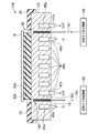
次に、本発明の第4の実施形態に係るウエハ載置台(基板載置台)について説明する。図9は、本発明の第4の実施形態に係るウエハ載置台を示す断面図である。本実施形態に係るウエハ載置台104は、載置台本体141を有し、その内部に外側冷媒循環路45aと内側冷媒循環路45bを有し、これらにはそれぞれ冷媒導入管46aおよび冷媒排出管47a、ならびに冷媒導入管46bおよび冷媒排出管47bが接続されており、互いに温度の異なる冷媒が通流されるようになっている。これにより、ウエハWに対して所定の温度分布を生じさせることが可能となっている。これら外側冷媒循環路45aと内側冷媒循環路45bとの間には、伝熱コントロール部160が設けられている。この伝熱コントロール部160は、円環状をなす空間部161と、空間部161内に充填された、多数の連通する空隙が存在する固体部材162とで構成されている、固体部材162は固体部材62と同様に構成される。空間部161には、その中に伝熱ガスを供給する供給配管164が接続されており、この供給配管164には伝熱ガス供給機構165が接続されている。また、空間部161には、空間部161内の伝熱ガスを排出する排出配管167が接続されており、この排出配管167には伝熱ガス排出機構168が接続されている。そして、供給する伝熱ガスの圧力を制御することにより、外側冷媒循環路45aと内側冷媒循環路45bとの間の熱伝達性を制御することにより、ウエハWの面内方向の温度勾配等を制御することができ、ウエハWの温度分布を高精度で制御することができる。<Fourth Embodiment>
Next, a wafer mounting table (substrate mounting table) according to a fourth embodiment of the present invention will be described. FIG. 9 is a sectional view showing a wafer mounting table according to the fourth embodiment of the present invention. The wafer mounting table 104 according to the present embodiment includes a mounting table
なお、本発明は上記実施形態に限定されることなく本発明の思想の範囲内で種々変形可能である。例えば、上記実施形態では、載置台本体の上部に載置部材として機能する静電チャックを設けたが、静電チャックは必須なものではない。静電チャックを用いない場合には、載置台本体の上面が載置面を有する載置部として機能する。また、上記実施形態では、熱源として冷媒流路を用い、冷媒の冷熱が載置台本体を伝熱して載置面に供給される例を示したが、熱源としてはヒーター等の加熱源を用いてもよく、その場合には熱が載置台本体を伝熱して載置面に供給される。さらに、上部電極および下部電極に高周波電力を印加するタイプの平行平板型プラズマエッチング装置を示したが、平行平板型に限らず、例えば誘導結合型プラズマ処理装置等、他の方式のプラズマ装置であってもよいし、エッチング処理に限らず、アッシングやCVD等、他の処理であってもよい。さらには、処理容器内を減圧にする処理であれば、プラズマ処理以外であってもよい。さらに、被処理基板は半導体ウエハに限るものではなく、フラットパネルディスプレイ基板等、他の基板であってもよい。 Note that the present invention is not limited to the above-described embodiment, and can be variously modified within the scope of the idea of the present invention. For example, in the above embodiment, the electrostatic chuck functioning as a mounting member is provided on the upper portion of the mounting table body, but the electrostatic chuck is not essential. When the electrostatic chuck is not used, the upper surface of the mounting table body functions as a mounting unit having a mounting surface. Moreover, in the said embodiment, although the refrigerant | coolant flow path was used as a heat source and the cold heat | fever of the refrigerant transferred the mounting base main body and was supplied to the mounting surface, the heating source, such as a heater, was used as a heat source. In this case, heat is transferred to the mounting surface by transferring heat through the mounting table main body. Furthermore, although a parallel plate type plasma etching apparatus of a type that applies high-frequency power to the upper electrode and the lower electrode has been shown, the present invention is not limited to a parallel plate type, and other types of plasma apparatuses such as an inductively coupled plasma processing apparatus. Alternatively, the process is not limited to the etching process, and may be another process such as ashing or CVD. Furthermore, as long as it is a process for reducing the pressure inside the processing container, it may be other than the plasma process. Furthermore, the substrate to be processed is not limited to a semiconductor wafer, and may be another substrate such as a flat panel display substrate.
1;プラズマ処理装置(プラズマエッチング装置)
2;チャンバ(処理室)
4;ウエハ載置台(基板載置台)
10;シャワーヘッド
20;処理ガス供給源
30;第1の高周波電源
41;載置台本体
42;静電チャック
55;He供給機構
60,60′、60″:伝熱コントロール部
61,61′、61″;空間部
61a;中央空間部
61b;外側空間部
61c;分離部材
62,62″,62a,62b;固体部材
65;伝熱ガス供給機構
68;伝熱ガス排出機構
70;第2の高周波電源
80;制御部1: Plasma processing equipment (plasma etching equipment)
2; chamber (processing room)
4; Wafer mounting table (substrate mounting table)
DESCRIPTION OF
Claims (20)
Translated fromJapanese載置台本体と、
前記載置台本体の上部に設けられた、基板を載置する載置面を有する載置部と、
冷熱または熱を前記載置台本体の上部に伝熱させるための熱源と、
前記載置台本体の伝熱経路中に位置し、載置された基板に対応するように設けられた空間部、および前記空間部に充填された、多数の連通する空隙が存在する固体部材を有し、前記空間部に伝熱ガスを供給または前記空間部から伝熱ガスを排出することにより、前記熱源からの伝熱をコントロールする伝熱コントロール部と、
前記空間部へ伝熱ガスを供給する伝熱ガス供給機構と、
前記空間部から伝熱ガスを排出する伝熱ガス排出機構と、
前記伝熱ガス供給機構による前記空間部への伝熱ガスの供給、前記伝熱ガス排出機構による前記空間部からの伝熱ガスの排出を制御する制御部と
を具備し、
前記固体部材は断熱材であることを特徴とする基板載置台。A substrate mounting table for mounting a substrate in a substrate processing apparatus,
A mounting table body;
A placement unit having a placement surface on which the substrate is placed, provided on the top of the placement table main body;
A heat source for transferring cold heat or heat to the top of the mounting table body,
A space portion provided in the heat transfer path of the mounting table main body and corresponding to the substrate placed thereon, and a solid member having a large number of communicating voids filled in the space portion. A heat transfer control unit for controlling heat transfer from the heat source by supplying heat discharge gas to the space or discharging heat transfer gas from the space;
A heat transfer gas supply mechanism for supplying a heat transfer gas to the space;
A heat transfer gas discharge mechanism for discharging heat transfer gas from the space,
A controller that controls supply of heat transfer gas to the space by the heat transfer gas supply mechanism and discharge of heat transfer gas from the space by the heat transfer gas discharge mechanism;
The substrate mounting table,wherein the solid member is a heat insulating material .
載置台本体と、
前記載置台本体の上部に設けられた、基板を載置する載置面を有する載置部と、
冷熱または熱を前記載置台本体の上部に伝熱させるための熱源と、
前記載置台本体の伝熱経路中に位置し、載置された基板に対応するように設けられた空間部、および前記空間部に充填された、多数の連通する空隙が存在する固体部材を有し、前記空間部に伝熱ガスを供給または前記空間部から伝熱ガスを排出することにより、前記熱源からの伝熱をコントロールする伝熱コントロール部と、
前記空間部へ伝熱ガスを供給する伝熱ガス供給機構と、
前記空間部から伝熱ガスを排出する伝熱ガス排出機構と、
前記伝熱ガス供給機構による前記空間部への伝熱ガスの供給、前記伝熱ガス排出機構による前記空間部からの伝熱ガスの排出を制御する制御部と
を具備し、
前記空間部に充填される前記固体部材は、基板の面内方向に沿って空隙率に分布が生じていることを特徴とする基板載置台。A substrate mounting table for mounting a substrate in a substrate processing apparatus,
A mounting table body;
A placement unit having a placement surface on which the substrate is placed, provided on the top of the placement table main body;
A heat source for transferring cold heat or heat to the top of the mounting table body,
A space portion provided in the heat transfer path of the mounting table main body and corresponding to the substrate placed thereon, and a solid member having a large number of communicating voids filled in the space portion. A heat transfer control unit for controlling heat transfer from the heat source by supplying heat discharge gas to the space or discharging heat transfer gas from the space;
A heat transfer gas supply mechanism for supplying a heat transfer gas to the space;
A heat transfer gas discharge mechanism for discharging heat transfer gas from the space,
A controller that controls supply of heat transfer gas to the space by the heat transfer gas supply mechanism, and discharge of heat transfer gas from the space by the heat transfer gas discharge mechanism;
Comprising
Wherein the solid member that is filled in the space portion,board mounting table characterized in that distribution of the porosity along the plane direction of the substrate occurs.
載置台本体と、
前記載置台本体の上部に設けられた、基板を載置する載置面を有する載置部と、
前記載置台本体内で異なる温度に保持され、冷熱または熱を前記載置台本体の上部に伝熱させる複数の熱源と、
前記載置台本体の前記複数の熱源の間に設けられた空間部、および前記空間部に充填された、多数の連通する空隙が存在する固体部材を有し、前記空間部に伝熱ガスを供給または前記空間部から伝熱ガスを排出することにより、前記複数の熱源の間の伝熱をコントロールする伝熱コントロール部と、
前記空間部へ伝熱ガスを供給する伝熱ガス供給機構と、
前記空間部から伝熱ガスを排出する伝熱ガス排出機構と、
前記伝熱ガス供給機構による前記空間部への伝熱ガスの供給、前記伝熱ガス排出機構による前記空間部からの伝熱ガスの排出を制御する制御部と
を具備し、
前記固体部材は断熱材であることを特徴とする基板載置台。A substrate mounting table for mounting a substrate in a substrate processing apparatus,
A mounting table body;
A placement unit having a placement surface on which the substrate is placed, provided on the top of the placement table main body;
A plurality of heat sources that are maintained at different temperatures in the mounting table main body and transfer cold or heat to the top of the mounting table main body,
A space portion provided between the plurality of heat sources of the mounting table main body, and a solid member filled with the space portion and having a large number of communicating gaps, and supplying heat transfer gas to the space portion Alternatively, a heat transfer control unit that controls heat transfer between the plurality of heat sources by discharging heat transfer gas from the space portion, and
A heat transfer gas supply mechanism for supplying a heat transfer gas to the space;
A heat transfer gas discharge mechanism for discharging heat transfer gas from the space,
A controller that controls supply of heat transfer gas to the space by the heat transfer gas supply mechanism and discharge of heat transfer gas from the space by the heat transfer gas discharge mechanism;
The substrate mounting table,wherein the solid member is a heat insulating material .
載置台本体と、 A mounting table body;
前記載置台本体の上部に設けられた、基板を載置する載置面を有する載置部と、 A placement unit having a placement surface on which the substrate is placed, provided on the top of the placement table main body;
冷熱または熱を前記載置台本体の上部に伝熱させるための熱源と、 A heat source for transferring cold heat or heat to the top of the mounting table body,
前記載置台本体の伝熱経路中に位置し、載置された基板に対応するように設けられた空間部、および前記空間部に充填された、多数の連通する空隙が存在する固体部材を有し、前記空間部に伝熱ガスを供給または前記空間部から伝熱ガスを排出することにより、前記熱源からの伝熱をコントロールする伝熱コントロール部と、 A space portion provided in the heat transfer path of the mounting table main body and corresponding to the substrate placed thereon, and a solid member having a large number of communicating voids filled in the space portion. A heat transfer control unit for controlling heat transfer from the heat source by supplying heat discharge gas to the space or discharging heat transfer gas from the space;
前記空間部へ伝熱ガスを供給する伝熱ガス供給機構と、 A heat transfer gas supply mechanism for supplying a heat transfer gas to the space;
前記空間部から伝熱ガスを排出する伝熱ガス排出機構と A heat transfer gas discharge mechanism for discharging heat transfer gas from the space portion;
を具備し、Comprising
前記固体部材は断熱材であることを特徴とする基板載置台。 The substrate mounting table, wherein the solid member is a heat insulating material.
前記処理容器内に設けられ、基板が載置され、請求項1から請求項18のいずれかに記載された構成を有する基板載置台と、
前記処理室内で基板に所定の処理を施す処理機構と
を具備することを特徴とする基板処理装置。A processing container that contains a substrate and whose inside is held under reduced pressure;
A substrate mounting table provided in the processing container, on which a substrate is mounted, and having a configuration according to any one of claims 1 to18 ,
And a processing mechanism for performing a predetermined process on the substrate in the processing chamber.
Priority Applications (2)
| Application Number | Priority Date | Filing Date | Title |
|---|---|---|---|
| JP2008297280AJP5198226B2 (en) | 2008-11-20 | 2008-11-20 | Substrate mounting table and substrate processing apparatus |
| US12/613,096US20100122774A1 (en) | 2008-11-20 | 2009-11-05 | Substrate mounting table and substrate processing apparatus having same |
Applications Claiming Priority (1)
| Application Number | Priority Date | Filing Date | Title |
|---|---|---|---|
| JP2008297280AJP5198226B2 (en) | 2008-11-20 | 2008-11-20 | Substrate mounting table and substrate processing apparatus |
Publications (2)
| Publication Number | Publication Date |
|---|---|
| JP2010123809A JP2010123809A (en) | 2010-06-03 |
| JP5198226B2true JP5198226B2 (en) | 2013-05-15 |
Family
ID=42171056
Family Applications (1)
| Application Number | Title | Priority Date | Filing Date |
|---|---|---|---|
| JP2008297280AExpired - Fee RelatedJP5198226B2 (en) | 2008-11-20 | 2008-11-20 | Substrate mounting table and substrate processing apparatus |
Country Status (2)
| Country | Link |
|---|---|
| US (1) | US20100122774A1 (en) |
| JP (1) | JP5198226B2 (en) |
Families Citing this family (46)
| Publication number | Priority date | Publication date | Assignee | Title |
|---|---|---|---|---|
| TWI508129B (en)* | 2007-10-31 | 2015-11-11 | Lam Res Corp | Temperature control module using gas pressure to control thermal conductance between liquid coolant and component body |
| JP5651317B2 (en)* | 2009-03-31 | 2015-01-07 | 東京エレクトロン株式会社 | Semiconductor manufacturing apparatus and temperature control method |
| US8435901B2 (en)* | 2010-06-11 | 2013-05-07 | Tokyo Electron Limited | Method of selectively etching an insulation stack for a metal interconnect |
| US8268184B2 (en)* | 2010-06-29 | 2012-09-18 | Tokyo Electron Limited | Etch process for reducing silicon recess |
| JP5642531B2 (en)* | 2010-12-22 | 2014-12-17 | 東京エレクトロン株式会社 | Substrate processing apparatus and substrate processing method |
| JP5822578B2 (en)* | 2011-07-20 | 2015-11-24 | 東京エレクトロン株式会社 | Mounting table temperature control apparatus and substrate processing apparatus |
| KR102110108B1 (en)* | 2011-09-30 | 2020-05-13 | 어플라이드 머티어리얼스, 인코포레이티드 | Electrostatic chuck |
| JP5905735B2 (en)* | 2012-02-21 | 2016-04-20 | 東京エレクトロン株式会社 | Substrate processing apparatus, substrate processing method, and method for changing settable band of substrate temperature |
| JP5863582B2 (en)* | 2012-07-02 | 2016-02-16 | 東京エレクトロン株式会社 | Plasma processing apparatus and temperature control method |
| JP5996340B2 (en)* | 2012-09-07 | 2016-09-21 | 東京エレクトロン株式会社 | Plasma etching equipment |
| US9018022B2 (en) | 2012-09-24 | 2015-04-28 | Lam Research Corporation | Showerhead electrode assembly in a capacitively coupled plasma processing apparatus |
| JP6165452B2 (en)* | 2013-02-01 | 2017-07-19 | 株式会社日立ハイテクノロジーズ | Plasma processing equipment |
| KR102112368B1 (en)* | 2013-02-28 | 2020-05-18 | 도쿄엘렉트론가부시키가이샤 | Mounting table and plasma processing apparatus |
| JP6173936B2 (en)* | 2013-02-28 | 2017-08-02 | 東京エレクトロン株式会社 | Mounting table and plasma processing apparatus |
| JP6069654B2 (en)* | 2013-03-29 | 2017-02-01 | Sppテクノロジーズ株式会社 | Plasma processing stage for substrate to be processed and plasma processing apparatus using the same |
| JP2015076457A (en)* | 2013-10-08 | 2015-04-20 | 株式会社日立ハイテクノロジーズ | Substrate processing equipment |
| JP6345030B2 (en)* | 2014-08-11 | 2018-06-20 | 東京エレクトロン株式会社 | Plasma processing apparatus and focus ring |
| JP6392612B2 (en)* | 2014-09-30 | 2018-09-19 | 日本特殊陶業株式会社 | Electrostatic chuck |
| JP5798677B2 (en)* | 2014-10-29 | 2015-10-21 | 東京エレクトロン株式会社 | Substrate processing apparatus and substrate processing method |
| US9805963B2 (en)* | 2015-10-05 | 2017-10-31 | Lam Research Corporation | Electrostatic chuck with thermal choke |
| JP6554387B2 (en)* | 2015-10-26 | 2019-07-31 | 東京エレクトロン株式会社 | Substrate cooling method in load lock apparatus, substrate transfer method, and load lock apparatus |
| JP6626753B2 (en)* | 2016-03-22 | 2019-12-25 | 東京エレクトロン株式会社 | Workpiece processing equipment |
| US10725485B2 (en)* | 2016-12-15 | 2020-07-28 | Lam Research Corporation | System and method for calculating substrate support temperature |
| JP6982394B2 (en)* | 2017-02-02 | 2021-12-17 | 東京エレクトロン株式会社 | Work piece processing device and mounting table |
| JP2018125461A (en)* | 2017-02-02 | 2018-08-09 | 東京エレクトロン株式会社 | Workpiece processing device |
| JP6392961B2 (en)* | 2017-09-13 | 2018-09-19 | 日本特殊陶業株式会社 | Electrostatic chuck |
| JP6522180B1 (en) | 2018-02-08 | 2019-05-29 | Sppテクノロジーズ株式会社 | Substrate mounting table, plasma processing apparatus provided with the same, and plasma processing method |
| JP6504532B1 (en)* | 2018-03-14 | 2019-04-24 | Toto株式会社 | Electrostatic chuck |
| JP6489277B1 (en)* | 2018-03-14 | 2019-03-27 | Toto株式会社 | Electrostatic chuck |
| JP7103910B2 (en)* | 2018-10-15 | 2022-07-20 | 東京エレクトロン株式会社 | Assembly status presentation device and assembly status presentation method |
| JP7002014B2 (en)* | 2018-10-30 | 2022-01-20 | Toto株式会社 | Electrostatic chuck |
| US11437261B2 (en) | 2018-12-11 | 2022-09-06 | Applied Materials, Inc. | Cryogenic electrostatic chuck |
| JP7401266B2 (en)* | 2018-12-27 | 2023-12-19 | 東京エレクトロン株式会社 | Substrate mounting table and substrate processing equipment |
| JP6729735B1 (en)* | 2019-03-05 | 2020-07-22 | Toto株式会社 | Electrostatic chuck |
| US11764041B2 (en) | 2019-06-14 | 2023-09-19 | Applied Materials, Inc. | Adjustable thermal break in a substrate support |
| US11373893B2 (en) | 2019-09-16 | 2022-06-28 | Applied Materials, Inc. | Cryogenic electrostatic chuck |
| CN113118965B (en)* | 2019-12-31 | 2022-09-30 | 清华大学 | Substrate loading and unloading control method |
| US11646183B2 (en) | 2020-03-20 | 2023-05-09 | Applied Materials, Inc. | Substrate support assembly with arc resistant coolant conduit |
| US12334315B2 (en) | 2020-04-30 | 2025-06-17 | Applied Materials, Inc. | Cooled substrate support assembly for radio frequency environments |
| US11087989B1 (en) | 2020-06-18 | 2021-08-10 | Applied Materials, Inc. | Cryogenic atomic layer etch with noble gases |
| US20230253193A1 (en)* | 2020-11-19 | 2023-08-10 | Lam Research Corporation | Substrate support with uniform temperature across a substrate |
| JP7575175B2 (en)* | 2020-12-22 | 2024-10-29 | 東京エレクトロン株式会社 | SUBSTRATE PROCESSING APPARATUS, TEMPERATURE CONTROL METHOD FOR SUBSTRATE PROCESSING APPARATUS, AND CONTROL DEVICE PROGRAM FOR CONTROLLING SUBSTRATE PROCESSING APPARATUS |
| JP2021093543A (en)* | 2021-02-26 | 2021-06-17 | 東京エレクトロン株式会社 | Workpiece processing device |
| US20230207289A1 (en)* | 2021-12-29 | 2023-06-29 | Semes Co., Ltd. | Support unit and apparatus for treating substrate with the unit |
| WO2024100876A1 (en)* | 2022-11-11 | 2024-05-16 | 日本碍子株式会社 | Wafer stage |
| WO2025154609A1 (en)* | 2024-01-15 | 2025-07-24 | 京セラ株式会社 | Sample holder |
Family Cites Families (34)
| Publication number | Priority date | Publication date | Assignee | Title |
|---|---|---|---|---|
| JPH0643140Y2 (en)* | 1985-03-05 | 1994-11-09 | 株式会社ブリヂストン | Breathable insulation |
| JP2905501B2 (en)* | 1989-07-08 | 1999-06-14 | 科学技術振興事業団 | Active thermal insulation method using fibrous body or porous body |
| JPH05243191A (en)* | 1992-02-26 | 1993-09-21 | Nec Corp | Dry etching device |
| JPH0680077A (en)* | 1992-09-02 | 1994-03-22 | Toshiba Corp | Vehicle door structure |
| JPH07249586A (en)* | 1993-12-22 | 1995-09-26 | Tokyo Electron Ltd | Treatment device and its manufacturing method and method for treating body to be treated |
| JP3411678B2 (en)* | 1994-07-08 | 2003-06-03 | 東京エレクトロン株式会社 | Processing equipment |
| JPH0914876A (en)* | 1995-06-26 | 1997-01-17 | Hazama Gumi Ltd | Heat storage pipe |
| US5846375A (en)* | 1996-09-26 | 1998-12-08 | Micron Technology, Inc. | Area specific temperature control for electrode plates and chucks used in semiconductor processing equipment |
| EP1008674B1 (en)* | 1997-04-11 | 2013-05-29 | Tokyo Electron Limited | Elecrode unit and processor |
| JP4256503B2 (en)* | 1997-10-30 | 2009-04-22 | 東京エレクトロン株式会社 | Vacuum processing equipment |
| JPH11307513A (en)* | 1998-04-20 | 1999-11-05 | Sony Corp | Plasma treating apparatus for insulator substrate |
| JP2001110883A (en)* | 1999-09-29 | 2001-04-20 | Applied Materials Inc | Substrate support device and heat transfer method thereof |
| JP2002009139A (en)* | 2000-06-20 | 2002-01-11 | Nikon Corp | Electrostatic chuck |
| JP2002305157A (en)* | 2000-12-28 | 2002-10-18 | Tokyo Electron Ltd | Honeycomb structure heat insulator and heat recycling system |
| JP4644943B2 (en)* | 2001-01-23 | 2011-03-09 | 東京エレクトロン株式会社 | Processing equipment |
| AU2002240261A1 (en)* | 2001-03-02 | 2002-09-19 | Tokyo Electron Limited | Method and apparatus for active temperature control of susceptors |
| EP1284251B1 (en)* | 2001-08-17 | 2011-09-28 | Eiji Tani | Silicon carbide-based, porous, lightweight, heat-resistant structural material and manufacturing method therefor |
| TW561515B (en)* | 2001-11-30 | 2003-11-11 | Tokyo Electron Ltd | Processing device, and gas discharge suppressing member |
| US6664738B2 (en)* | 2002-02-27 | 2003-12-16 | Hitachi, Ltd. | Plasma processing apparatus |
| JP2004014752A (en)* | 2002-06-06 | 2004-01-15 | Tokyo Electron Ltd | Electrostatic chuck, work piece placement table, and plasma treating apparatus |
| US7347901B2 (en)* | 2002-11-29 | 2008-03-25 | Tokyo Electron Limited | Thermally zoned substrate holder assembly |
| JP4063689B2 (en)* | 2003-02-19 | 2008-03-19 | 株式会社日立製作所 | Plasma processing equipment |
| US20040261946A1 (en)* | 2003-04-24 | 2004-12-30 | Tokyo Electron Limited | Plasma processing apparatus, focus ring, and susceptor |
| KR100538690B1 (en)* | 2003-07-16 | 2005-12-23 | 한국기계연구원 | Highly Porous Ceramics Fabricated From Preceramic Polymers And Expandable Microspheres, And The Producing Method The Same |
| US6992892B2 (en)* | 2003-09-26 | 2006-01-31 | Tokyo Electron Limited | Method and apparatus for efficient temperature control using a contact volume |
| US20060027169A1 (en)* | 2004-08-06 | 2006-02-09 | Tokyo Electron Limited | Method and system for substrate temperature profile control |
| US7544251B2 (en)* | 2004-10-07 | 2009-06-09 | Applied Materials, Inc. | Method and apparatus for controlling temperature of a substrate |
| US20060090855A1 (en)* | 2004-10-29 | 2006-05-04 | Tokyo Electron Limited | Substrate mounting table, substrate processing apparatus and substrate temperature control method |
| JP4350695B2 (en)* | 2004-12-01 | 2009-10-21 | 株式会社フューチャービジョン | Processing equipment |
| US7789962B2 (en)* | 2005-03-31 | 2010-09-07 | Tokyo Electron Limited | Device and method for controlling temperature of a mounting table, a program therefor, and a processing apparatus including same |
| JP2006344670A (en)* | 2005-06-07 | 2006-12-21 | Renesas Technology Corp | Manufacturing method of semiconductor device |
| JP2007258500A (en)* | 2006-03-24 | 2007-10-04 | Hitachi High-Technologies Corp | Substrate support device |
| US8294068B2 (en)* | 2008-09-10 | 2012-10-23 | Applied Materials, Inc. | Rapid thermal processing lamphead with improved cooling |
| JP5357639B2 (en)* | 2009-06-24 | 2013-12-04 | 株式会社日立ハイテクノロジーズ | Plasma processing apparatus and plasma processing method |
- 2008
- 2008-11-20JPJP2008297280Apatent/JP5198226B2/ennot_activeExpired - Fee Related
- 2009
- 2009-11-05USUS12/613,096patent/US20100122774A1/ennot_activeAbandoned
Also Published As
| Publication number | Publication date |
|---|---|
| JP2010123809A (en) | 2010-06-03 |
| US20100122774A1 (en) | 2010-05-20 |
Similar Documents
| Publication | Publication Date | Title |
|---|---|---|
| JP5198226B2 (en) | Substrate mounting table and substrate processing apparatus | |
| JP7725518B2 (en) | Substrate processing apparatus and mounting table | |
| US11342167B2 (en) | Plasma processing method including cleaning of inside of chamber main body of plasma processing apparatus | |
| CN108346568B (en) | Method of handling the processed object | |
| CN107039229B (en) | Engraving method | |
| JP5357639B2 (en) | Plasma processing apparatus and plasma processing method | |
| CN100382276C (en) | Substrate placing table, substrate processing device, and substrate processing method | |
| US8124539B2 (en) | Plasma processing apparatus, focus ring, and susceptor | |
| TWI433232B (en) | An upper electrode, a plasma processing device, and a plasma processing method | |
| JP5270310B2 (en) | Electrostatic chuck and substrate processing apparatus | |
| JP5492578B2 (en) | Plasma processing equipment | |
| JP2008251742A (en) | Substrate treating apparatus, and substrate mounting base on which focus ring is mounted | |
| JP2009212340A (en) | Electrode unit, substrate treatment apparatus, and temperature control method for electrode unit | |
| KR102332028B1 (en) | Substrate processing method and substrate processing device | |
| JP2009010101A (en) | Substrate processing equipment, and showerhead | |
| JP2002009064A (en) | Sample processing apparatus and sample processing method | |
| JP5503503B2 (en) | Plasma processing equipment | |
| US20060090855A1 (en) | Substrate mounting table, substrate processing apparatus and substrate temperature control method | |
| JPH10223621A (en) | Vacuum treating apparatus | |
| JP2007123796A (en) | Structure for plasma treatment chamber, plasma treatment chamber, and plasma treatment device | |
| JP2003224077A (en) | Plasma processor, electrode member, manufacturing method for baffle plate, processor and surface treatment method | |
| JP2019201086A (en) | Processing device, component, and temperature control method | |
| JPH09289201A (en) | Plasma treating apparatus | |
| JP4642550B2 (en) | Substrate mounting table, substrate processing apparatus, and substrate temperature control method | |
| US20040085706A1 (en) | Electrostatic chuck, supporting table and plasma processing system |
Legal Events
| Date | Code | Title | Description |
|---|---|---|---|
| A621 | Written request for application examination | Free format text:JAPANESE INTERMEDIATE CODE: A621 Effective date:20111024 | |
| A977 | Report on retrieval | Free format text:JAPANESE INTERMEDIATE CODE: A971007 Effective date:20121011 | |
| A131 | Notification of reasons for refusal | Free format text:JAPANESE INTERMEDIATE CODE: A131 Effective date:20121016 | |
| A521 | Request for written amendment filed | Free format text:JAPANESE INTERMEDIATE CODE: A523 Effective date:20121214 | |
| TRDD | Decision of grant or rejection written | ||
| A01 | Written decision to grant a patent or to grant a registration (utility model) | Free format text:JAPANESE INTERMEDIATE CODE: A01 Effective date:20130108 | |
| A61 | First payment of annual fees (during grant procedure) | Free format text:JAPANESE INTERMEDIATE CODE: A61 Effective date:20130206 | |
| FPAY | Renewal fee payment (event date is renewal date of database) | Free format text:PAYMENT UNTIL: 20160215 Year of fee payment:3 | |
| R150 | Certificate of patent or registration of utility model | Free format text:JAPANESE INTERMEDIATE CODE: R150 Ref document number:5198226 Country of ref document:JP Free format text:JAPANESE INTERMEDIATE CODE: R150 | |
| R250 | Receipt of annual fees | Free format text:JAPANESE INTERMEDIATE CODE: R250 | |
| R250 | Receipt of annual fees | Free format text:JAPANESE INTERMEDIATE CODE: R250 | |
| R250 | Receipt of annual fees | Free format text:JAPANESE INTERMEDIATE CODE: R250 | |
| R250 | Receipt of annual fees | Free format text:JAPANESE INTERMEDIATE CODE: R250 | |
| R250 | Receipt of annual fees | Free format text:JAPANESE INTERMEDIATE CODE: R250 | |
| LAPS | Cancellation because of no payment of annual fees |