JP5190986B2 - Nonvolatile semiconductor memory device and manufacturing method thereof - Google Patents
Nonvolatile semiconductor memory device and manufacturing method thereofDownload PDFInfo
- Publication number
- JP5190986B2 JP5190986B2JP2008028579AJP2008028579AJP5190986B2JP 5190986 B2JP5190986 B2JP 5190986B2JP 2008028579 AJP2008028579 AJP 2008028579AJP 2008028579 AJP2008028579 AJP 2008028579AJP 5190986 B2JP5190986 B2JP 5190986B2
- Authority
- JP
- Japan
- Prior art keywords
- gate
- floating gate
- oxide film
- film
- memory device
- Prior art date
- Legal status (The legal status is an assumption and is not a legal conclusion. Google has not performed a legal analysis and makes no representation as to the accuracy of the status listed.)
- Expired - Fee Related
Links
Images


Classifications
- H—ELECTRICITY
- H10—SEMICONDUCTOR DEVICES; ELECTRIC SOLID-STATE DEVICES NOT OTHERWISE PROVIDED FOR
- H10D—INORGANIC ELECTRIC SEMICONDUCTOR DEVICES
- H10D30/00—Field-effect transistors [FET]
- H10D30/60—Insulated-gate field-effect transistors [IGFET]
- H10D30/68—Floating-gate IGFETs
- H10D30/681—Floating-gate IGFETs having only two programming levels
- H10D30/684—Floating-gate IGFETs having only two programming levels programmed by hot carrier injection
- H10D30/685—Floating-gate IGFETs having only two programming levels programmed by hot carrier injection from the channel
- H—ELECTRICITY
- H10—SEMICONDUCTOR DEVICES; ELECTRIC SOLID-STATE DEVICES NOT OTHERWISE PROVIDED FOR
- H10B—ELECTRONIC MEMORY DEVICES
- H10B41/00—Electrically erasable-and-programmable ROM [EEPROM] devices comprising floating gates
- H10B41/30—Electrically erasable-and-programmable ROM [EEPROM] devices comprising floating gates characterised by the memory core region
- H—ELECTRICITY
- H10—SEMICONDUCTOR DEVICES; ELECTRIC SOLID-STATE DEVICES NOT OTHERWISE PROVIDED FOR
- H10D—INORGANIC ELECTRIC SEMICONDUCTOR DEVICES
- H10D30/00—Field-effect transistors [FET]
- H10D30/01—Manufacture or treatment
- H10D30/021—Manufacture or treatment of FETs having insulated gates [IGFET]
- H10D30/0411—Manufacture or treatment of FETs having insulated gates [IGFET] of FETs having floating gates
- H—ELECTRICITY
- H10—SEMICONDUCTOR DEVICES; ELECTRIC SOLID-STATE DEVICES NOT OTHERWISE PROVIDED FOR
- H10D—INORGANIC ELECTRIC SEMICONDUCTOR DEVICES
- H10D30/00—Field-effect transistors [FET]
- H10D30/60—Insulated-gate field-effect transistors [IGFET]
- H10D30/68—Floating-gate IGFETs
- H10D30/6891—Floating-gate IGFETs characterised by the shapes, relative sizes or dispositions of the floating gate electrode
- H10D30/6892—Floating-gate IGFETs characterised by the shapes, relative sizes or dispositions of the floating gate electrode having at least one additional gate other than the floating gate and the control gate, e.g. program gate, erase gate or select gate
- H—ELECTRICITY
- H10—SEMICONDUCTOR DEVICES; ELECTRIC SOLID-STATE DEVICES NOT OTHERWISE PROVIDED FOR
- H10D—INORGANIC ELECTRIC SEMICONDUCTOR DEVICES
- H10D64/00—Electrodes of devices having potential barriers
- H10D64/01—Manufacture or treatment
- H10D64/031—Manufacture or treatment of data-storage electrodes
- H10D64/035—Manufacture or treatment of data-storage electrodes comprising conductor-insulator-conductor-insulator-semiconductor structures
- G—PHYSICS
- G11—INFORMATION STORAGE
- G11C—STATIC STORES
- G11C16/00—Erasable programmable read-only memories
- G11C16/02—Erasable programmable read-only memories electrically programmable
- G11C16/04—Erasable programmable read-only memories electrically programmable using variable threshold transistors, e.g. FAMOS
- G11C16/0408—Erasable programmable read-only memories electrically programmable using variable threshold transistors, e.g. FAMOS comprising cells containing floating gate transistors
- G11C16/0433—Erasable programmable read-only memories electrically programmable using variable threshold transistors, e.g. FAMOS comprising cells containing floating gate transistors comprising cells containing a single floating gate transistor and one or more separate select transistors
Landscapes
- Non-Volatile Memory (AREA)
- Semiconductor Memories (AREA)
- Element Separation (AREA)
Description
Translated fromJapanese本発明は、スプリットゲート型の不揮発性半導体記憶装置及びその製造方法に関する。特に、本発明は、消去ゲートを備えるスプリットゲート型の不揮発性半導体記憶装置及びその製造方法に関する。 The present invention relates to a split gate nonvolatile semiconductor memory device and a method for manufacturing the same. In particular, the present invention relates to a split gate type nonvolatile semiconductor memory device having an erase gate and a method for manufacturing the same.
電気的に消去/プログラム可能な不揮発性半導体記憶装置として、フラッシュメモリやEEPROM等が知られている。そのような不揮発性半導体記憶装置のメモリセルは、典型的には、フローティングゲートとコントロールゲートを備えるトランジスタである。コントロールゲートは、フローティングゲート上に積層される場合もあるし、フローティングゲート側方のチャネル領域上に少なくとも形成される場合もある。後者は、一般的に「スプリットゲート型」と呼ばれ、過消去対策や読み出し速度向上等の観点から優れている。 Flash memory, EEPROM, and the like are known as electrically erasable / programmable nonvolatile semiconductor memory devices. A memory cell of such a nonvolatile semiconductor memory device is typically a transistor having a floating gate and a control gate. The control gate may be stacked on the floating gate or may be formed at least on the channel region on the side of the floating gate. The latter is generally called a “split gate type” and is excellent from the viewpoints of over-erasing countermeasures and reading speed improvement.
上記メモリセルに対する一般的なデータプログラム/消去方法は、次の通りである。データプログラムは、CHE(Channel Hot Electron)方式で実現される。具体的には、コントロールゲートとドレインにそれぞれ所定のプログラム電位が印加され、ドレイン近傍で発生するホットエレクトロンがフローティングゲートに注入される。一方、データ消去は、FN(Fowler-Nordheim)トンネル方式で実現される。具体的には、コントロールゲートに高電位が印加され、FNトンネリングにより、フローティングゲート中の電子がトンネル絶縁膜を通してコントロールゲートへ引き抜かれる。 A general data program / erase method for the memory cell is as follows. The data program is realized by a CHE (Channel Hot Electron) method. Specifically, predetermined program potentials are applied to the control gate and the drain, respectively, and hot electrons generated near the drain are injected into the floating gate. On the other hand, data erasure is realized by an FN (Fowler-Nordheim) tunnel method. Specifically, a high potential is applied to the control gate, and electrons in the floating gate are extracted to the control gate through the tunnel insulating film by FN tunneling.
ここで、次の問題点が考えられる。上述のスプリットゲート型の場合、コントロールゲートは、チャネル領域上にゲート絶縁膜を介して形成される。また、上述の通り、データ消去時には、FNトンネリングを実現するために、コントロールゲートには高電位を印加する必要がある。従って、信頼性の観点から、高電位が印加されるコントロールゲート直下のゲート絶縁膜を薄くすることが出来ない。コントロールゲートとチャネル領域の間のゲート絶縁膜を薄く出来ない場合、データ読み出し時の読み出し電流が減少し、読み出し速度が低下するという問題が生じる。 Here, the following problems can be considered. In the case of the split gate type described above, the control gate is formed on the channel region via a gate insulating film. Further, as described above, when erasing data, it is necessary to apply a high potential to the control gate in order to realize FN tunneling. Therefore, from the viewpoint of reliability, the gate insulating film directly under the control gate to which a high potential is applied cannot be thinned. When the gate insulating film between the control gate and the channel region cannot be thinned, there arises a problem that the read current at the time of data reading decreases and the reading speed decreases.
このような問題を解決するために、データ消去用の「消去ゲート(erase gate)」を、コントロールゲートとは別に設ける技術が提案されている(特許文献1、特許文献2、特許文献3参照)。データ消去時には、コントロールゲートではなくこの消去ゲートに高電位が印加される。その結果、FNトンネリングにより、フローティングゲート中の電子が消去ゲートに引き抜かれる。データ消去時にコントロールゲートに高電位を印加する必要がなくなるため、コントロールゲート直下のゲート絶縁膜を薄くすることが可能となる。その結果、読み出し速度の低下が防止される。 In order to solve such a problem, a technique has been proposed in which an “erase gate” for erasing data is provided separately from the control gate (see
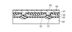
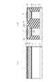
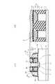
図1は、特許文献1に開示されたメモリセルを示している。シリコン基板60上にLOCOS(Local Oxidation of Silicon)法により素子分離膜72が形成されている。また、シリコン基板60上にゲート酸化膜63を介してフローティングゲート64が形成されている。そのフローティングゲート64上には、選択酸化法により選択酸化膜66が形成されている。選択酸化膜66は、フローティングゲート64の中央部で厚く形成され、結果としてフローティングゲート64の上面が窪む。更に、素子分離膜72、フローティングゲート64の側面、及び選択酸化膜66を覆うようにトンネル酸化膜67が形成され、そのトンネル酸化膜67上に消去ゲート68が形成されている。消去ゲート68上には酸化膜69が形成されている。図1に示されるように、消去ゲート68は、選択酸化膜66及びトンネル酸化膜67を挟んでフローティングゲート64の上面と対向し、且つ、トンネル酸化膜67を挟んでフローティングゲート64の側面と対向している。そのフローティングゲート64の側面は鉛直である。 FIG. 1 shows a memory cell disclosed in
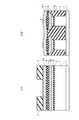
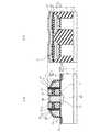
図2は、特許文献2に開示されたメモリセルを示している。シリコン基板80中にソース領域81及びドレイン領域82が形成されている。また、シリコン基板80上にゲート酸化膜83を介してフローティングゲート84及びコントロールゲート85が形成されている。更に、ソース領域81上にはゲート酸化膜83及びトンネル酸化膜87を介して消去ゲート86が形成されている。フローティングゲート84と消去ゲート86の間にはトンネル酸化膜87が介在しており、フローティングゲート84とコントロールゲート85の間には酸化膜88が介在している。更に、ドレイン領域82、コントロールゲート85及び消去ゲート86の上面上には、それぞれシリサイド膜89、90及び91が形成されている。図2に示されるように、消去ゲート86は、ソース領域81上に形成され、トンネル酸化膜87を挟んでフローティングゲート84の上面の一部及び側面全体と対向している。そのフローティングゲート84の側面は鉛直である。 FIG. 2 shows a memory cell disclosed in
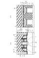
図3は、特許文献3に開示されたメモリセルを示している。シリコン基板100中にソース領域101及びドレイン領域102が形成されている。チャネル領域上にはゲート絶縁膜103、104を介してコントロールゲート105及びフローティングゲート106がそれぞれ形成されている。コントロールゲート105上には酸化膜109が形成されている。ソース領域101上にはソース配線110が形成されている。更に、フローティングゲート106、酸化膜109及びソース配線110を覆うようにトンネル酸化膜108が形成されており、そのトンネル酸化膜108上に消去ゲート107が形成されている。図3に示されるように、フローティングゲート106は鉛直な第1側面と湾曲した第2側面を有している。第1側面と第2側面はフローティングゲート106の上端部で互いにつながっており、第1側面と第2側面の間隔はその上端部からシリコン基板100側に向けて広くなっている。つまり、フローティングゲート106は上端部に向かって尖っている。消去ゲート107は、トンネル酸化膜108を挟んでフローティングゲート106の上端部と対向している。 FIG. 3 shows a memory cell disclosed in
本願発明者は、次の点に着目した。消去効率を向上させるために、消去ゲートと対向するフローティングゲートの鋭角部での電界集中を利用することが考えられる。電界集中をより強めるためには、フローティングゲートの鋭角部をより尖らせることが望ましい。 The inventor of the present application paid attention to the following points. In order to improve the erase efficiency, it is conceivable to use electric field concentration at the acute angle portion of the floating gate facing the erase gate. In order to increase the electric field concentration, it is desirable to sharpen the acute angle portion of the floating gate.
以下に、[発明を実施するための最良の形態]で使用される番号・符号を用いて、[課題を解決するための手段]を説明する。これらの番号・符号は、[特許請求の範囲]の記載と[発明を実施するための最良の形態]との対応関係を明らかにするために括弧付きで付加されたものである。ただし、それらの番号・符号を、[特許請求の範囲]に記載されている発明の技術的範囲の解釈に用いてはならない。 [Means for Solving the Problems] will be described below using the numbers and symbols used in [Best Mode for Carrying Out the Invention]. These numbers and symbols are added in parentheses in order to clarify the correspondence between the description of [Claims] and [Best Mode for Carrying Out the Invention]. However, these numbers and symbols should not be used for the interpretation of the technical scope of the invention described in [Claims].
本発明の第1の観点において、不揮発性半導体記憶装置が提供される。その不揮発性半導体記憶装置は、半導体基板(1)と、半導体基板(1)中のチャネル領域上のゲート絶縁膜(20,2)上に並んで形成されたコントロールゲート(22)及びフローティングゲート(3)と、フローティングゲート(3)の上面(FUS)と対向する消去ゲート(10)と、を備える。フローティングゲート(3)の側面は、対向する第1側面(FSS1)と第2側面(FSS2)を含む。第1側面(FSS1)と第2側面(FSS2)の間隔は、上面(FUS)から半導体基板(1)側に向かうにつれて狭くなる。 In a first aspect of the present invention, a nonvolatile semiconductor memory device is provided. The nonvolatile semiconductor memory device includes a semiconductor substrate (1), a control gate (22) formed on the gate insulating film (20, 2) on the channel region in the semiconductor substrate (1), and a floating gate ( 3) and an erase gate (10) facing the upper surface (FUS) of the floating gate (3). The side surface of the floating gate (3) includes a first side surface (FSS1) and a second side surface (FSS2) that face each other. The distance between the first side surface (FSS1) and the second side surface (FSS2) becomes narrower from the upper surface (FUS) toward the semiconductor substrate (1) side.
本発明の第2の観点において、不揮発性半導体記憶装置が提供される。その不揮発性半導体記憶装置は、半導体基板(1)と、半導体基板(1)中のチャネル領域上のゲート絶縁膜(20,2)上に並んで形成されたコントロールゲート(22)及びフローティングゲート(3)と、フローティングゲート(3)の上面(FUS)と対向する消去ゲート(10)と、を備える。フローティングゲート(3)の底面(FBS)の幅(W2)は、フローティングゲート(3)の上面(FUS)の幅(W1)よりも狭い。 In a second aspect of the present invention, a nonvolatile semiconductor memory device is provided. The nonvolatile semiconductor memory device includes a semiconductor substrate (1), a control gate (22) formed on the gate insulating film (20, 2) on the channel region in the semiconductor substrate (1), and a floating gate ( 3) and an erase gate (10) facing the upper surface (FUS) of the floating gate (3). The width (W2) of the bottom surface (FBS) of the floating gate (3) is narrower than the width (W1) of the top surface (FUS) of the floating gate (3).
本発明の第3の観点において、不揮発性半導体記憶装置の製造方法が提供される。まず、第1素子分離構造(6−1)と第2素子分離構造(6−2)が形成される。ここで、第1素子分離構造(6−1)及び第2素子分離構造(6−2)は、半導体基板(1)から突出する第1突出部(PR1)及び第2突出部(PR2)をそれぞれ有する。次に、第1突出部(PR1)と第2突出部(PR2)のそれぞれの上端部をエッチングすることにより、第1素子分離構造(6−1)の上面(SUS1)と側面(SSS1)とをつなぐ第1傾斜面(SLP1)と、第2素子分離構造(6−2)の上面(SUS2)と側面(SSS2)とをつなぐ第2傾斜面(SLP2)が形成される。ここで、第1傾斜面(SLP1)と第2傾斜面(SLP2)は対向しており、第1傾斜面(SLP1)と第2傾斜面(SLP2)の間隔は半導体基板(1)から離れるにつれて広くなる。次に、半導体基板(1)上の第1ゲート絶縁膜(2)上に、第1突出部(PR1)と第2突出部(PR2)とに挟まれるフローティングゲート(3)が形成される。ここで、フローティングゲート(3)の両側面(FSS1、FSS2)は第1傾斜面(SLP1)及び第2傾斜面(SLP2)のそれぞれと接触し、フローティングゲート(3)の上面(FUS)は消去ゲート(10)と対向する。次に、フローティングゲート(3)と並ぶコントロールゲート(22)が、半導体基板(1)上の第2ゲート絶縁膜(20)上に形成される。 In a third aspect of the present invention, a method for manufacturing a nonvolatile semiconductor memory device is provided. First, the first element isolation structure (6-1) and the second element isolation structure (6-2) are formed. Here, the first element isolation structure (6-1) and the second element isolation structure (6-2) include a first protrusion (PR1) and a second protrusion (PR2) protruding from the semiconductor substrate (1). Have each. Next, the upper surface (SUS1) and the side surface (SSS1) of the first element isolation structure (6-1) are etched by etching the upper ends of the first protrusion (PR1) and the second protrusion (PR2). And a second inclined surface (SLP2) connecting the upper surface (SUS2) and the side surface (SSS2) of the second element isolation structure (6-2). Here, the first inclined surface (SLP1) and the second inclined surface (SLP2) face each other, and the distance between the first inclined surface (SLP1) and the second inclined surface (SLP2) increases as the distance from the semiconductor substrate (1) increases. Become wider. Next, a floating gate (3) sandwiched between the first protrusion (PR1) and the second protrusion (PR2) is formed on the first gate insulating film (2) on the semiconductor substrate (1). Here, both side surfaces (FSS1, FSS2) of the floating gate (3) are in contact with the first inclined surface (SLP1) and the second inclined surface (SLP2), and the upper surface (FUS) of the floating gate (3) is erased. Opposite the gate (10). Next, a control gate (22) aligned with the floating gate (3) is formed on the second gate insulating film (20) on the semiconductor substrate (1).
本発明によれば、フローティングゲートの第1側面と第2側面の間隔が、上面から半導体基板側に向かうにつれて狭くなる。つまり、フローティングゲートの両側面が内側に向かっている。従って、消去ゲートと対向するフローティングゲートの上面の両端部がより尖ることになる。これにより、フローティングゲートの上面の両端部での電界集中が強まり、結果として消去効率と消去速度が向上する。 According to the present invention, the distance between the first side surface and the second side surface of the floating gate becomes narrower from the upper surface toward the semiconductor substrate side. That is, both side surfaces of the floating gate face inward. Therefore, both ends of the upper surface of the floating gate facing the erase gate are sharper. As a result, the electric field concentration at both ends of the upper surface of the floating gate is increased, and as a result, the erase efficiency and the erase speed are improved.
添付図面を参照して、本発明の実施の形態に係る不揮発性半導体記憶装置及びその製造方法を説明する。 A nonvolatile semiconductor memory device and a manufacturing method thereof according to embodiments of the present invention will be described with reference to the accompanying drawings.
1.概要
図4は、本発明の実施の形態に係る不揮発性半導体記憶装置のメモリセルを概略的に示している。半導体基板1上にはゲート絶縁膜を介してフローティングゲート3が形成されている。また、フローティングゲート3の上面FUSと対向するように消去ゲート10が形成されている。1. Overview FIG. 4 schematically shows a memory cell of a nonvolatile semiconductor memory device according to an embodiment of the present invention. A floating
フローティングゲート3の側面は、互いに対向する第1側面FSS1と第2側面FSS2を含んでいる。また、フローティングゲート3の上面FUSは、互いに対向する第1辺FE1及び第2辺FE2を含んでおり、第1辺FE1において第1側面FSS1とつながり、第2辺FE2において第2側面FSS2とつながっている。本実施の形態によれば、第1側面FSS1と第2側面FSS2の間隔は、上面FUSから半導体基板1側に向かうにつれて狭くなる。つまり、フローティングゲート3の両側面FSS1、FSS2が内側に向かって湾曲している。その結果、図4に示されるように、フローティングゲート3の底面FBSの幅W2は、上面FUSの幅W1よりも狭くなる。 The side surface of the floating
データ消去時、フローティングゲート3中の電子は、フローティングゲート3から消去ゲート10に引き抜かれる。上述の通り、フローティングゲート3の第1側面FSS1と第2側面FSS2の間隔は、上面FUSから半導体基板1側に向かうにつれて狭くなる。従って、消去ゲート10と対向するフローティングゲート3の上面FUSの両端部(FE1、FE2)がより尖ることになる。これにより、フローティングゲート3の上面FUSの両端部(FE1、FE2)での電界集中が強まり、結果として消去効率と消去速度が向上する。 At the time of data erasure, electrons in the floating
2.構造例
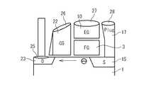
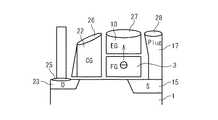
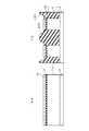
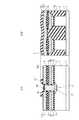
以下、本実施の形態に係る不揮発性半導体記憶装置の一例を詳しく説明する。図5は、本例に係る不揮発性半導体記憶装置の平面図(平面レイアウト)である。図6A及び図6Bはそれぞれ、図5中の線A−A’及び線B−B’に沿った断面構造を示している。2. Structural Example Hereinafter, an example of the nonvolatile semiconductor memory device according to this embodiment will be described in detail. FIG. 5 is a plan view (planar layout) of the nonvolatile semiconductor memory device according to this example. 6A and 6B show cross-sectional structures taken along lines AA ′ and BB ′ in FIG. 5, respectively.
図5において、破線で囲まれた部分が1bit分のメモリセルに相当する。B−B’に平行な方向に、消去ゲート(EG)10、コントロールゲート(CG)22、及びプラグ(PLUG)17が形成されている。消去ゲート10及びコントロールゲート22は、プラグ17に対して対称に配置されている。プラグ17、消去ゲート10及びコントロールゲート22は、B−B’方向に延伸しており、B−B’方向に並ぶメモリセル間で共有される。一方、A−A’に平行な方向に、素子分離構造としてSTI(Shallow Trench Isolation)6、及び金属配線層(bit−line)32が形成されている。金属配線層32は、メモリセルにつながるコンタクトプラグ(CT)31に接続されており、プラグ17、消去ゲート10及びコントロールゲート22の上層に形成されている。また、各メモリセルは、フローティングゲート(FG)3を有している。各メモリセルにおいて、フローティングゲート3は、消去ゲート10の下層に形成されており、また、隣り合うSTI6間に挟まれている。 In FIG. 5, a portion surrounded by a broken line corresponds to a 1-bit memory cell. An erase gate (EG) 10, a control gate (CG) 22, and a plug (PLUG) 17 are formed in a direction parallel to B-B '. The erase
図6Aには、図5中の線A−A’に沿った2個のメモリセルの断面構造が示されている。半導体基板であるシリコン基板1内には、Pウェル7が形成されている。Pウェル7の表面には、N型の不純物領域でありソースあるいはドレインとなる第1ソース/ドレイン拡散層15及び第2ソース/ドレイン拡散層23が形成されている。第2ソース/ドレイン拡散層23は、LDD構造を有している。プラグ17は、第1ソース/ドレイン拡散層15上に形成されており、第1ソース/ドレイン拡散層15と電気的に接続されている。プラグ17の上面には、コバルトシリサイド膜28が形成されている。一方、コンタクトプラグ31は、第2ソース/ドレイン拡散層23上に形成されている。第2ソース/ドレイン拡散層23の表層(上面)には、コバルトシリサイド膜25が形成されており、コンタクトプラグ31はコバルトシリサイド膜25を介して第2ソース/ドレイン拡散層23に電気的に接続されている。コンタクトプラグ31につながる金属配線層32は、層間絶縁膜29上に形成されている。 FIG. 6A shows a cross-sectional structure of two memory cells along the line A-A ′ in FIG. 5. A P well 7 is formed in a
プラグ17の両側には、第2酸化膜サイドウォールスペーサー16を挟んで、フローティングゲート3が形成されている。フローティングゲート3は、第1ポリシリコン膜(第1導電膜)3aと第2ポリシリコン膜(第2導電膜)3bとから構成されており、2層構造を有している。フローティングゲート3とシリコン基板1(Pウェル7)との間には、第1ゲート酸化膜2が形成されている。フローティングゲート3は、第1ソース/ドレイン拡散層15の一部とオーバーラップしており、第1ゲート酸化膜2を通して第1ソース/ドレイン拡散層15と容量結合している。また、第2酸化膜サイドウォールスペーサー16に対向する側のフローティングゲート3の側面には、第3酸化膜サイドウォールスペーサー19及び第2ゲート酸化膜20が形成されている。更に、フローティングゲート3上には、酸化膜8及びトンネル酸化膜9が形成されている。このようにフローティングゲート3は、周囲を絶縁膜で囲まれており、外部から電気的に隔離されている。 Floating
フローティングゲート3の直上には、酸化膜8及びトンネル酸化膜9を介して、消去ゲート10が形成されている。消去ゲート10の両側面には、フローティングゲート3と同様に、第2酸化膜サイドウォールスペーサー16、第3酸化膜サイドウォールスペーサー19及び第2ゲート酸化膜20が形成されている。消去ゲート10の上面はシリサイド化され、コバルトシリサイド膜27が形成されている。後述されるように、この消去ゲート10は、データ消去時に用いられる。 An erase
更に、シリコン基板1(Pウェル7)表層のチャネル領域上に、第2ゲート酸化膜20を介してコントロールゲート22が形成されている。つまり、コントロールゲート22とフローティングゲート3は、チャネル領域上のゲート酸化膜(2、20)上に並んで形成されている。これは、スプリットゲート型のメモリセルの特徴である。コントロールゲート22とフローティングゲート3の間には、第3酸化膜サイドウォールスペーサー19及び第2ゲート酸化膜20が介在している。コントロールゲート22の他方の側面には、第4酸化膜サイドウォールスペーサー24が形成されている。また、コントロールゲート22の上面はシリサイド化され、コバルトシリサイド膜26が形成されている。 Further, a
このように、第2ソース/ドレイン拡散層23、コントロールゲート22、消去ゲート10及びプラグ17の上面の全てがシリサイド化されている。これにより、配線抵抗を十分に低減することが可能となる。 Thus, all of the upper surfaces of the second source /
尚、図6Aに示されるように、隣接するメモリセル同士は、第1ソース/ドレイン拡散層15(プラグ17)を共用する。そして、それぞれのメモリセルは、第1ソース/ドレイン拡散層15(プラグ17)に対して、対称に形成されている。つまり、第1ソース/ドレイン拡散層15(プラグ17)に対して、フローティングゲート3、消去ゲート10及びコントロールゲート22等が、対称に形成されている。 As shown in FIG. 6A, adjacent memory cells share the first source / drain diffusion layer 15 (plug 17). Each memory cell is formed symmetrically with respect to the first source / drain diffusion layer 15 (plug 17). That is, the floating
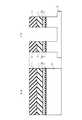
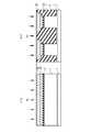
図6Bには、図5中の線B−B’に沿った2個のメモリセルの断面構造が示されている。素子分離構造としてのSTI6は、シリコン基板1(Pウェル7)中に形成され、且つ、シリコン基板1(Pウェル7)から突出するように形成されている。各STI6の上端部は削られており、傾斜面が形成されている。 FIG. 6B shows a cross-sectional structure of two memory cells along the line B-B ′ in FIG. 5. The
隣り合うSTI6の間のシリコン基板1(Pウェル7)上には、第1ゲート酸化膜2を介してフローティングゲート3が形成されている。フローティングゲート3は、隣り合う2つのSTI6に挟まれている。また、フローティングゲート3は、第1ポリシリコン膜(第1導電膜)3aと第2ポリシリコン膜(第2導電膜)3bとから構成されており、2層構造を有している。このうち第2ポリシリコン膜3bは、STI6と一部重なるように形成されている。また、第2ポリシリコン膜3bの上面は中央部が窪むように形成されており、且つ、第2ポリシリコン膜3bの両側面は内側に湾曲するように形成されている。その結果、第2ポリシリコン膜3bの上面角部には、STI6側に張り出すような鋭い鋭角部3cが形成されている。鋭角部3cの角度は例えば30〜40度程度である。 A floating
フローティングゲート3の上面上には酸化膜8が形成されている。酸化膜8は、フローティングゲート3の中央部上で最も厚くなっており、端部に向かうにつれて薄くなっている。トンネル酸化膜9は、酸化膜8、フローティングゲート3の鋭角部3c、及びSTI6を覆うように形成されている。つまり、フローティングゲート3の上面の鋭角部3cは、トンネル酸化膜9に接触している。 An
トンネル酸化膜9上には消去ゲート10が形成されている。消去ゲート10は、フローティングゲート3の上面と対向している。ここで、フローティングゲート3と消去ゲート10の距離は、フローティングゲート3の鋭角部3cの箇所で一番近くなっており、その距離はトンネル酸化膜9の膜厚である。つまり、消去ゲート10は、トンネル酸化膜9を挟んで特にフローティングゲート3の鋭角部3cと対向している。 An erase
消去ゲート10上にはコバルトシリサイド膜27が形成されている。コバルトシリサイド膜27上には層間絶縁膜29が形成されている。 A
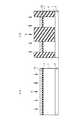
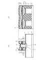
図7は、図6Bで示されたメモリセルの構造を概略的に示している。図7を参照して、本例におけるフローティングゲート3、素子分離構造(STI)6、消去ゲート10の形状や位置関係を更に詳しく説明する。 FIG. 7 schematically shows the structure of the memory cell shown in FIG. 6B. With reference to FIG. 7, the shape and positional relationship of the floating
シリコン基板1には第1素子分離構造6−1と第2素子分離構造6−2が形成されている。第1素子分離構造6−1と第2素子分離構造6−2は互いに平行である(図5参照)。第1素子分離構造6−1は、シリコン基板1から突出する第1突出部PR1を有し、第2素子分離構造6−2は、シリコン基板1から突出する第2突出部PR2を有している。第1突出部PR1は、第1素子分離構造6−1の上面SUS1と側面SSS1をつなぐ湾曲した第1傾斜面SLP1を有している。一方、第2突出部PR2は、第2素子分離構造6−2の上面SUS2と側面SSS2をつなぐ湾曲した第2傾斜面SLP2を有している。それら第1傾斜面SLP1と第2傾斜面SLP2は対向しており、第1傾斜面SLP1と第2傾斜面SLP2の間隔はシリコン基板1から離れるにつれて広くなっている。 A first element isolation structure 6-1 and a second element isolation structure 6-2 are formed on the
フローティングゲート3は、第1ゲート酸化膜2を介してシリコン基板1上に形成されている。フローティングゲート3の側面は、互いに対向する第1側面FSS1と第2側面FSS2を含んでいる。また、フローティングゲート3の上面FUSは、互いに対向する第1辺FE1及び第2辺FE2を含んでおり、第1辺FE1において第1側面FSS1とつながり、第2辺FE2において第2側面FSS2とつながっている。 The floating
フローティングゲート3の上面FUSは窪んでおり(湾曲しており)、第1辺FE1及び第2辺FE2は、第1辺FE1と第2辺FE2との間の上面FUSよりも上に位置している。つまり、フローティングゲート3は、第1辺FE1と第2辺FE2において上述の「鋭角部3c」を有している。尚、鋭角部3cの数は2個に限られず、1個であってもよいし、3個以上であってもよい。 The upper surface FUS of the floating
また、フローティングゲート3は、上述の第1突出部PR1と第2突出部PR2に挟まれている。より詳細には、フローティングゲート3の第1側面FSS1及び第2側面FSS2は、上述の第1傾斜面SLP1及び第2傾斜面SLP2のそれぞれと接触している。よって、第1側面FSS1と第2側面FSS2の間隔は、上面FUSからシリコン基板1側に向かうにつれて狭くなる。つまり、フローティングゲート3の両側面FSS1、FSS2が内側に向かって湾曲している。その結果、フローティングゲート3の底面FBSの幅W2は、上面FUSの幅W1よりも狭くなる。また、上面FUSの第1辺FE1及び第2辺FE2における「鋭角部3c」は更に鋭くなる。 In addition, the floating
また、フローティングゲート3は、上述の第1傾斜面SLP1及び第2傾斜面SLP2よりシリコン基板1側に位置する部分を少なくとも有している。より詳細には、フローティングゲート3は、シリコン基板1上に第1ゲート酸化膜2を介して形成された第1導電膜3aと、その第1導電膜3a上に形成された第2導電膜3bとを含んでいる。このうち第1導電膜3aの下面FBSは、第1傾斜面SLP1及び第2傾斜面SLP2よりもシリコン基板1側に位置している。すなわち、第1導電膜3aの少なくとも一部は、第1傾斜面SLP1及び第2傾斜面SLP2よりも下方に位置している。 Further, the floating
消去ゲート10は、フローティングゲート3の上面FUSと対向するように形成されている。ここで、消去ゲート10の全体が、フローティングゲート3の上面FUSよりも上に位置している。従って、消去ゲート10は、フローティングゲート3の側面と対向しない。また、消去ゲート10の底面EBSと第1辺FE1、第2辺FE2との間隔はそれぞれT1、T2である。一方、消去ゲート10の底面EBSと辺FE1−FE2間の上面FUSとの間隔は、上記T1、T2よりも大きいT3である(T3>T1、T2)。すなわち、消去ゲート10の底面EBSは、フローティングゲート3の第1辺FE1と第2辺FE2との間の上面FUSよりも、第1辺FE1及び第2辺FE2に近い。 Erase
以上に説明された特徴は、既出の図4で説明された特徴を包含していることに留意されたい。 It should be noted that the features described above include the features described in FIG.
3.動作
次に、本例に係るメモリセルに対するデータ書き込み、データ読み出し、及びデータ消去を説明する。3. Operation Next, data writing, data reading, and data erasing with respect to the memory cell according to this example will be described.
(データ書き込み)
図8を参照して、データ書き込みを説明する。図8には、線A−A’に沿った構造が概念的に示されている。書き込みは、ソースサイドチャネルホットエレクトロン(CHE:Channel Hot Electron)注入よって行われる。書き込み動作時においては、第1ソース/ドレイン拡散層15は、ドレイン(D)として、第2ソース/ドレイン拡散層23はソース(S)として、それぞれ機能する。例えば、コントロールゲート22には+1.6Vの電圧が印加され、第1ソース/ドレイン拡散層15には+7.6Vの電圧が印加され、第2ソース/ドレイン拡散層23には+0.3Vの電圧が印加される。第2ソース/ドレイン拡散層23から放出された電子は、チャネル領域の強電界により加速され、CHEとなる。特に、第1ソース/ドレイン拡散層15とフローティングゲート3との間の容量結合によってフローティングゲート3の電位も高くなっており、コントロールゲート22とフローティングゲート3との間の狭いギャップには、強電界が発生する。その強電界により生成された高エネルギーのCHEが、ゲート酸化膜2を通してフローティングゲート3に注入される。このような注入は、ソースサイドインジェクション(SSI:Source Side Injection)と呼ばれ、SSIによれば、電子注入効率が向上し、印加電圧を低く設定することが可能となる。フローティングゲート3に電子が注入されることにより、メモリセルトランジスタの閾値電圧が上昇する。(Data writing)
Data writing will be described with reference to FIG. FIG. 8 conceptually shows the structure along the line AA ′. Writing is performed by source side channel hot electron (CHE) injection. During the write operation, the first source /
また、書き込み動作時、消去ゲート10に電圧を印加してもよい(例えば、4〜5V)。すなわち、消去ゲート10がフローティングゲート3の電位を持ち上げる役割を担っても良い。この場合には、第1ソース/ドレイン拡散層15に印加する電圧を下げることができるため、第1ソース/ドレイン拡散層15と第2ソース/ドレイン拡散層23の間(ソース−ドレイン間)のパンチスルー耐性を上げることが可能になる。 Further, a voltage may be applied to the erase
(データ読み出し)
図9を参照して、データ読み出しを説明する。図9には、線A−A’に沿った構造が概念的に示されている。読み出し動作時には、第1ソース/ドレイン拡散層15は、ソース(S)として、第2ソース/ドレイン拡散層23は、ドレイン(D)として、それぞれ機能する。例えば、コントロールゲート22には+2.7Vの電圧が印加され、第2ソース/ドレイン拡散層23には+0.5Vの電圧が印加され、第1ソース/ドレイン拡散層15及びシリコン基板1の電圧は0Vに設定される。消去セル(例えば、フローティングゲート3に電荷が注入されていない状態のメモリセル)の場合、閾値電圧は低く、読み出し電流(メモリセル電流)が流れる。一方、書き込み(プログラム)セル(例えば、フローティングゲート3に電荷が注入されている状態のメモリセル)の場合、閾値電圧は高く、読み出し電流(メモリセル電流)がほとんど流れない。この読み出し電流(メモリセル電流)を検出することによって、プログラムセルか消去セルかを判定(データ0が記憶されているのかデータ1が記憶されているのかを判定)することができる。(Data read)
With reference to FIG. 9, data reading will be described. FIG. 9 conceptually shows the structure along the line AA ′. During the read operation, the first source /
(データ消去)
図10A及び図10Bを参照して、データ消去を説明する。図10Aには、線A−A’に沿った構造が概念的に示されており、図10Bには、線B−B’に沿った構造が概念的に示されている。データ消去は、FNトンネル方式で行われる。例えば、消去ゲート10には10Vの電圧が印加され、コントロールゲート22、第1ソース/ドレイン拡散層15、第2ソース/ドレイン拡散層23及びシリコン基板1の電圧は、0Vに設定される。その結果、消去ゲート10とフローティングゲート3との間のトンネル絶縁膜9に高電界が印加され、FNトンネル電流が流れる。これによりフローティングゲート3内の電子が、トンネル絶縁膜9を通じて、消去ゲート10に引き抜かれる。(erase data)
Data erasure will be described with reference to FIGS. 10A and 10B. FIG. 10A conceptually shows the structure along the line AA ′, and FIG. 10B conceptually shows the structure along the line BB ′. Data erasure is performed by the FN tunnel method. For example, a voltage of 10V is applied to the erase
特に、消去ゲート10に近いフローティングゲート3の鋭角部3c(第1辺FE1及び第2辺FE2)の周辺には、尖り形状により強い電界集中が発生する。従って、図10Bに示されるように、フローティングゲート3内の電子は、主としてその鋭角部3cから消去ゲート10に放出される。フローティングゲート3の鋭角部3cは、電子の引き抜き効率を向上させていると言える。このように、本実施の形態によれば、消去ゲート10と対向するフローティングゲート3の鋭角部3cにより、消去効率と消去速度が向上する。 In particular, a strong electric field concentration is generated around the
フローティングゲート3から電子が引き抜かれることにより、メモリセルの閾値電圧が減少する。尚、過消去によりフローティングゲート3に関する閾値電圧が負になった場合、フローティングゲート3の下部のシリコン基板1(Pウェル7)内には、チャネルが常時発生し得る。しかしながら、チャネル領域上にはコントロールゲート22も設けられているため、メモリセルが常にオン状態となってしまうことを防止できる。このように、スプリットゲート型は、過剰消去エラーが防止されるという利点を有する。 By extracting electrons from the floating
また、上述の通り、消去動作時には、コントロールゲート22とは別に設けられた消去ゲート10に高電圧が印加され、消去ゲート10とフローティングゲート3との間でFNトンネリングが発生する。コントロールゲート22に高電圧を印加する必要がないため、コントロールゲート22直下の第2ゲート酸化膜20の劣化は発生しない。従って、第2ゲート酸化膜20を薄くすることが可能となる。その結果、低電圧でもデータ読み出し時のメモリセル電流を大きくすることでき、読み出し速度が向上する。 Further, as described above, during the erase operation, a high voltage is applied to the erase
4.製造方法の例
以下、図11〜図49を参照して、本実施の形態に係る不揮発性半導体記憶装置の製造方法の一例を説明する。図11〜図49の各々には、各製造工程におけるA−A’断面構造及びB−B’断面構造が示されている。4). Example of Manufacturing Method Hereinafter, an example of a method of manufacturing the nonvolatile semiconductor memory device according to the present embodiment will be described with reference to FIGS. Each of FIGS. 11 to 49 shows an AA ′ sectional structure and a BB ′ sectional structure in each manufacturing process.
まず、図11に示されるように、熱酸化法により、シリコン基板1上に8〜10nm程度の膜厚の第1ゲート酸化膜2が形成される。続いて、CVD法により、80〜100nm程度の膜厚の第1ポリシリコン膜3aが、第1ゲート酸化膜2上に形成される。第1ポリシリコン膜3aは、フローティングゲート3の一部となる材料膜(第1ゲート材料膜)である。更に、CVD法により、100nm〜150nm程度の膜厚のフィールド窒化膜4が、第1ポリシリコン膜3a上に形成される。 First, as shown in FIG. 11, a first
次に、図12に示されるように、素子分離構造形成のための第1レジストマスク5が、フィールド窒化膜4上に形成される。第1レジストマスク5は、A−A’に平行な方向に開口パターンを有している。 Next, as shown in FIG. 12, a first resist
次に、図13に示されるように、第1レジストマスク5をマスクとして用いることにより、異方性ドライエッチングが実施される。その結果、フィールド窒化膜4、第1ポリシリコン膜3a及び第1ゲート酸化膜2が順次選択的に除去される。更に、300nm程度の深さまでシリコン基板1がエッチングされ、トレンチが形成される。各トレンチは、A−A’に平行な方向に沿っている。その後、第1レジストマスク5が剥離される。 Next, as shown in FIG. 13, anisotropic dry etching is performed by using the first resist
次に、プラズマCVD法により、600〜700nm程度の膜厚の酸化膜が全面に堆積される。その後、CMP(Chemical Mechanical Polishing)により、酸化膜の表面がフィールド窒化膜4の上面と同じ高さになるように平坦化される。その結果、図14に示されるように、素子分離構造としてのSTI6が、前工程で形成されたトレンチを埋めるように形成される。つまり、各STI6は、フィールド窒化膜4、第1ポリシリコン膜3a及び第1ゲート酸化膜2を貫通してシリコン基板1の内部に達するように形成される。図14に示されるように、各STI6はシリコン基板1から突出するように形成されており、突出部(PR1、PR2;図7参照)を有している。尚、各STI6は、A−A’に平行な方向に沿っている。 Next, an oxide film having a thickness of about 600 to 700 nm is deposited on the entire surface by plasma CVD. Thereafter, the surface of the oxide film is planarized by CMP (Chemical Mechanical Polishing) so that the surface of the oxide film is flush with the upper surface of the
次に、図15に示されるように、140〜160度程度のリン酸液中に30〜40分程度浸すことによって、フィールド窒化膜4が除去される。 Next, as shown in FIG. 15, the
次に、図16に示されるように、例えば注入エネルギー130〜150keV、ドーズ量4.0×10¹²〜6.0×1012cm−2で、ボロン(B)のイオン注入が実施される。ボロンは、第1ポリシリコン膜3a及び第1ゲート酸化膜2を通過してシリコン基板1へ注入される。その後、活性化のため、窒素雰囲気中900〜1000度程度の温度で熱処理が実施される。その結果、シリコン基板1内にPウェル7が形成される。Next, as shown in FIG. 16, boron (B) ion implantation is performed at an implantation energy of 130 to 150 keV and a dose of 4.0 × 10¹² to 6.0 × 1012 cm−2 , for example. Boron passes through the
次に、フッ酸を用いて酸化膜ウェットエッチングが3〜4分実施される。その結果、図17に示されるように、各STI6(突出部PR1,PR2)の上端角部がエッチングされ、各STI6に湾曲した傾斜面(SLP1,SLP2;図7参照)が形成される。図17に示されるように、隣り合うSTI6のそれぞれの傾斜面SLP1、SLP2は、互いに対向しており、傾斜面SLP1、SLP2の間隔は、シリコン基板1から離れるにつれて広くなっている。尚、当該エッチング工程より前に第1ポリシリコン膜3aが既に形成されていることに留意されたい。この第1ポリシリコン膜3aは、上述の傾斜面(SLP1,SLP2)よりシリコン基板1側に位置する部分を少なくとも有している。逆に言えば、当該エッチングは、傾斜面(SLP1,SLP2)が第1ポリシリコン膜3aの下面(第1ゲート酸化膜2の上面)よりも上方に形成されるように実施される。よって、過剰なエッチングにより半導体基板1まで削れてしまい、いわゆる「ディボット(divot)」が発生することが防止される。第1ポリシリコン膜3aは、当該エッチング工程において半導体基板1を保護する役割を果たしており、ディボットの発生を防止する。本実施の形態によれば、ディボットを発生させることなく、STI6の傾斜面(SLP1,SLP2)は適切に形成される。 Next, oxide film wet etching is performed for 3 to 4 minutes using hydrofluoric acid. As a result, as shown in FIG. 17, the upper end corners of the respective STIs 6 (projections PR1, PR2) are etched, and curved inclined surfaces (SLP1, SLP2; see FIG. 7) are formed in the
次に、図18に示されるように、CVD法により、300〜400nm程度の膜厚の第2ポリシリコン膜3bが全面に堆積される。この第2ポリシリコン膜3bは、第1ポリシリコン膜3aと同様に、フローティングゲート3の一部となる材料膜(第2ゲート材料膜)である。 Next, as shown in FIG. 18, a
次に、図19に示されるように、CMPにより、第2ポリシリコン膜3bの表面がSTI6の上面と同じ高さになるように平坦化される。その結果、第2ポリシリコン膜3bが、第1ポリシリコン膜3a上においてSTI6の傾斜面(SLP1,SLP2)に挟まれるように形成される。この第2ポリシリコン膜3bの両側面は、STI6とオーバーラップしており、STI6の傾斜面(SLP1,SLP2)と接触している。このようにして、フローティングゲート3の材料となる第1ポリシリコン膜3aと第2ポリシリコン膜3bから、A−A’方向に延在する構造(以下、「ゲート構造」と参照される)が形成される。このゲート構造は、第1ゲート酸化膜2上に形成されており、隣り合うSTI6(突出部PR1,PR2;図7参照)間に挟まれている。後述されるように、このゲート構造をパターンニングすることによりフローティングゲート3が形成される。図19に示されるように、ゲート構造の上面は、A−A’に沿った第1辺FE1と第2辺FE2を含んでいる。これら第1辺FE1及び第2辺FE2が、上述のフローティングゲート3の上面の鋭角部3cとなる。 Next, as shown in FIG. 19, the surface of the
次に、図20に示されるように、第1ポリシリコン膜3a及び第2ポリシリコン膜3bを導電化するために、N型不純物(例:砒素(As)、注入エネルギー:5keV、ドーズ量:1.0×1015cm−2)が全面に注入される。あるいは、リン酸トリクロリド(POCL3)を熱拡散源として第1ポリシリコン膜3a及び第2ポリシリコン膜3bにリンドープを行ってもよい。その後、活性化のため、窒素雰囲気中800度程度の温度で熱処理が実施される。Next, as shown in FIG. 20, in order to make the
次に、図21に示されるように、第2ポリシリコン膜3bの上面上に絶縁膜が形成される。ここでは、熱酸化法が採用され、第2ポリシリコン膜3bの表層に酸化膜8が形成される。このとき、酸化膜8は、中央部が最も厚く、端部に近づくほど薄くなるように形成される。そのため、第2ポリシリコン膜3bの上面FUSは、窪み形状(湾曲形状)を有するようになる。結果として、上面FUSの第1辺FE1と第2辺FE2における鋭角部3cは更に鋭くなり、30〜40度程度の鋭角形状となる。 Next, as shown in FIG. 21, an insulating film is formed on the upper surface of the
次に、図22に示されるように、酸化膜8及びSTI6の表面が、フッ酸を用いることにより10nm程度エッチング除去される。その結果、第2ポリシリコン膜3bの鋭角部3cが露出する。 Next, as shown in FIG. 22, the surfaces of the
次に、図23に示されるように、CVD法により、14〜16nm程度の膜厚のトンネル酸化膜9が全面に堆積される。トンネル酸化膜9は、酸化膜8、第2ポリシリコン膜3bの鋭角部3c、及びSTI6を覆うように形成されている。つまり、第2ポリシリコン膜3bの鋭角部3cはトンネル酸化膜9に接触している。このようにして、上述のゲート構造上に、酸化膜8とトンネル酸化膜9からなる絶縁膜が形成される。ゲート構造上の絶縁膜の厚さは、第1辺FE1と第2辺FE2との間よりも、第1辺FE1及び第2辺FE2上で薄い。つまり、ゲート構造上の絶縁膜は、中央部が最も厚く、端部に近づくほど薄くなる。なお、トンネル酸化膜9を形成した後、熱酸化を行って熱酸化膜を更に形成してもよい。 Next, as shown in FIG. 23, a
次に、図24に示されるように、CVD法により、トンネル酸化膜9上に第3ポリシリコン膜10aが形成される。この第3ポリシリコン膜10aは、消去ゲート10となる材料膜(第3ゲート材料膜)である。この第3ポリシリコン膜10aは、フローティングゲート3となるゲート構造の上面と対向している。特に、第3ポリシリコン膜10aは、トンネル酸化膜9を挟んで第2ポリシリコン膜3bの鋭角部3c(第1辺FE1、第2辺FE2)に対向している。また、ゲート構造がSTI6の突出部間の領域に埋め込まれており、トンネル酸化膜9がSTI6を覆うように形成されているため、そのトンネル酸化膜9上に形成される第3ポリシリコン膜10aは、必然的にゲート構造の上面よりも上に位置することになる。つまり、第3ポリシリコン膜10aは、ゲート構造の側面と対向していない。 Next, as shown in FIG. 24, a
次に、図25に示されるように、CVD法により、200〜300nm程度の膜厚の窒化膜11が全面に堆積される。 Next, as shown in FIG. 25, a
次に、図26に示されるように、第2レジストマスク12が窒化膜11上に形成される。第2レジストマスク12は、B−B’に平行な方向に開口パターンを有している。 Next, as shown in FIG. 26, the second resist
次に、図27に示されるように、異方性ドライエッチングにより、窒化膜11が選択的に除去される。これにより、窒化膜11は、B−B’に平行な方向に開口パターンを有するようになる。その後、第2レジストマスク12が剥離される。 Next, as shown in FIG. 27, the
次に、CVD法により150〜200nm程度の膜厚の酸化膜が全面に堆積された後、エッチバックが実施される。その結果、図28に示されるように、窒化膜11の開口部側面に第1酸化膜サイドウォールスペーサー13が形成される。この第1酸化膜サイドウォールスペーサー13の幅は、フローティングゲート3のゲート長を決定するものとなる。 Next, after an oxide film having a thickness of about 150 to 200 nm is deposited on the entire surface by a CVD method, etch back is performed. As a result, as shown in FIG. 28, the first oxide
次に、図29に示されるように、第1酸化膜サイドウォールスペーサー13をマスクとして用いることにより、異方性ドライエッチングが実施される。これにより、第3ポリシリコン膜10a、トンネル酸化膜9、酸化膜8、第2ポリシリコン膜3b、第1ポリシリコン膜3a、及び第2ゲート酸化膜2が、順次選択的に除去される。その結果、シリコン基板1(Pウェル7)上に開口部が形成される。 Next, as shown in FIG. 29, anisotropic dry etching is performed by using the first oxide
次に、図30に示されるように、10〜20nm程度の膜厚の酸化膜14が全面に形成される。続いて、N型不純物のイオン注入が実施された後、活性化のため窒素雰囲気中1000度程度の温度で熱処理が行われる。これにより、開口部下のシリコン基板1(Pウェル7)内に、第1ソース/ドレイン拡散層15が形成される。イオン注入は、例えば、注入エネルギー40keV、ドーズ量1.0×1014cm−2で、砒素(As)を注入し、さらに、注入エネルギー30keV、ドーズ量1.0×1014cm−2で、リン(P)を注入することで行われる。尚、第1ソース/ドレイン拡散層15の一部は、第1ゲート酸化膜2の下に潜り込む、すなわち、第1ポリシリコン膜3a及び第2ポリシリコン膜3bにオーバーラップするように形成される。Next, as shown in FIG. 30, an
次に、図31に示されるように、異方性ドライエッチングにより、酸化膜14がエッチバックされる。これにより、第1ソース/ドレイン拡散層15上の開口部の側壁を覆うように第2酸化膜サイドウォールスペーサー16が形成される。第2酸化膜サイドウォールスペーサー16は、第1酸化膜サイドウォールスペーサー13、第3ポリシリコン膜10a、トンネル酸化膜9、酸化膜8、第2ポリシリコン膜3b、第1ポリシリコン膜3a及び第2ゲート酸化膜2の側壁を覆っている。 Next, as shown in FIG. 31, the
次に、図32に示されるように、500〜600nm程度の膜厚の第4ポリシリコン膜17aが形成される。この第4ポリシリコン膜17aは、第1ソース/ドレイン拡散層15につながるプラグ17の材料膜であり、第1ソース/ドレイン拡散層15上の開口部に埋め込まれている。第4ポリシリコン膜17aには、例えば1.0×1019cm−2〜5.0×1020cm−2程度のリンがドープされている。Next, as shown in FIG. 32, a
次に、図33に示されるように、CMPにより、窒化膜11の表面が露出するまで第4ポリシリコン膜17aの表面が平坦化される。つまり、第4ポリシリコン膜17aの表面が窒化膜11の上面と同じ高さになるように平坦化される。 Next, as shown in FIG. 33, the surface of the
次に、図34に示されるように、第4ポリシリコン膜17aの高さが低くなるように、第4ポリシリコン膜17aの一部がエッチングされる。当該エッチングは、第4ポリシリコン膜17aの上面が、第3ポリシリコン膜10aの上面から30〜50nm程度上方になるように行われる。 Next, as shown in FIG. 34, a part of the
次に、図35に示されるように、第1酸化膜サイドウォールスペーサー13の上面が第4ポリシリコン膜17aの上面と同じ高さになるまで、第1酸化膜サイドウォールスペーサー13の一部がエッチングされる。 Next, as shown in FIG. 35, until the upper surface of the first oxide
次に、図36に示されるように、第4ポリシリコン膜17aの上面が第3ポリシリコン膜10aの上面から30〜50nm程度下方になるように、第4ポリシリコン膜17aの一部がエッチングされる。これにより、第1ソース/ドレイン拡散層15につながるプラグ17が完成する。 Next, as shown in FIG. 36, a part of the
次に、図37に示されるように、800〜900度の温度で熱酸化を行うことにより、プラグ17の上面に20〜50nm程度の膜厚のプラグ酸化膜18が形成される。 Next, as shown in FIG. 37, by performing thermal oxidation at a temperature of 800 to 900 degrees, a
次に、図38に示されるように、140〜160度程度のリン酸液中に60〜100分程度浸すことによって、窒化膜11が除去される。 Next, as shown in FIG. 38, the
次に、図39に示されるように、第1酸化膜サイドウォールスペーサー13、第2酸化膜サイドウォールスペーサー16及びプラグ酸化膜18をマスクとして用いることにより、異方性ドライエッチングが実施される。これにより、第3ポリシリコン膜10a、トンネル酸化膜9、酸化膜8、第2ポリシリコン膜3b、第1ポリシリコン膜3aが、順次選択的に除去される。このとき、第1ゲート酸化膜2の露出部の膜厚は、ドライエッチングの影響で5nm程度まで薄くなる。本工程は、消去ゲート10及びフローティングゲート3を形成するためのパターンニング工程に相当する。つまり、第3ポリシリコン膜10a及びゲート構造(第1ポリシリコン膜3a、第2ポリシリコン膜3b)をパターンニングすることにより、第3ポリシリコン膜10aから消去ゲート10が形成され、ゲート構造(3a、3b)からフローティングゲート3が形成される。形成される消去ゲート10及びフローティングゲート3は、既出の図7で説明された特徴を有している。 Next, as shown in FIG. 39, anisotropic dry etching is performed by using the first oxide
次に、20〜30nm程度の膜厚の酸化膜が全面に形成された後、異方性ドライエッチングが実施される。これにより、図40に示されるように、第1酸化膜サイドウォールスペーサー13、消去ゲート10、トンネル酸化膜9、酸化膜8、フローティングゲート3及び第1ゲート酸化膜2の側面に、第3酸化膜サイドウォールスペーサー19が形成される。尚、このドライエッチングにより、前述の露出していた5nm程度の膜厚の第1ゲート酸化膜2は除去される。また、このドライエッチングより、第1酸化膜サイドウォールスペーサー13が薄くなる。 Next, after an oxide film having a thickness of about 20 to 30 nm is formed on the entire surface, anisotropic dry etching is performed. As a result, as shown in FIG. 40, the third oxide
次に、図41に示されるように、CVD法により、5〜7nm程度の膜厚の第2ゲート酸化膜20が全面に堆積される。このとき、第2ゲート酸化膜20は、シリコン基板1(Pウェル7)の露出領域上の他、第3酸化膜サイドウォールスペーサー19の側壁にも形成される。そのため、第1酸化膜サイドウォールスペーサー13、消去ゲート10、トンネル酸化膜9、酸化膜8、フローティングゲート3及び第1ゲート酸化膜2の側壁には、2層の酸化膜(第3酸化膜サイドウォールスペーサー19及び第2ゲート酸化膜20)が形成されることになる。続いて、1000度程度の酸素雰囲気や窒素雰囲気、若しくは酸素と窒素の混合された雰囲気でアニール処理を行ってもよい。また、800〜900度で熱酸化を行うことにより、第2ゲート酸化膜20が形成されてもよい。 Next, as shown in FIG. 41, a second
次に、図42に示されるように、CVD法により、200〜300nm程度の膜厚のリンドープされた第5ポリシリコン膜21が全面に堆積される。この第5ポリシリコン膜21は、コントロールゲート22の材料となる材料膜である。 Next, as shown in FIG. 42, a phosphorus-doped
次に、図43に示されるように、第5ポリシリコン膜21がエッチバックされ、コントロールゲート22が形成される。このコントロールゲート22は、シリコン基板1(Pウェル7)上に第2ゲート酸化膜20上を介して形成されている。また、コントロールゲート22は、第3酸化膜サイドウォールスペーサー19及び第2ゲート酸化膜20を挟んで、消去ゲート10、トンネル酸化膜9、酸化膜8、フローティングゲート3及び第1ゲート酸化膜2の側方に形成される。つまり、シリコン基板1上でフローティングゲート3とコントロールゲート22は並んで形成される。尚、本工程において、コントロールゲート22に隣接するシリコン基板1(Pウェル7)上には、2〜4nm程度の膜厚の第2ゲート酸化膜20が残存する。 Next, as shown in FIG. 43, the
次に、図44に示されるように、N型不純物(例:砒素(As)、注入エネルギー:10〜20keV、ドーズ量:1.0×1013cm−2)が全面にイオン注入される。その後、活性化のため、窒素雰囲気中1000度程度の温度で熱処理が実施される。その結果、低濃度の拡散層23aが、前述の残存している第2ゲート酸化膜20下のシリコン基板1(Pウェル7)内に形成される。Next, as shown in FIG. 44, an N-type impurity (for example, arsenic (As), implantation energy: 10 to 20 keV, dose amount: 1.0 × 1013 cm−2 ) is ion-implanted over the entire surface. Thereafter, heat treatment is performed at a temperature of about 1000 ° C. in a nitrogen atmosphere for activation. As a result, a low-
次に、CVD法により80〜100nm程度の膜厚の酸化膜が形成された後、エッチバックが実施される。その結果、図45に示されるように、コントロールゲート22の側壁に第4酸化膜サイドウォールスペーサー24が形成される。このエッチバックの際に、低濃度拡散層23a上の第2ゲート酸化膜20と、消去ゲート10上の酸化膜(第1酸化膜サイドウォールスペーサー13及び第2ゲート酸化膜20)と、プラグ17上の酸化膜(プラグ酸化膜18及び第2ゲート酸化膜20)も、同時に除去される。 Next, after an oxide film having a thickness of about 80 to 100 nm is formed by the CVD method, etch back is performed. As a result, as shown in FIG. 45, a fourth oxide film
次に、図46に示されるように、N型不純物(例:砒素(As)、注入エネルギー:30〜60keV、ドーズ量:3.0×1015cm−2〜5.0×1015cm−2)が全面にイオン注入される。その後、活性化のため、窒素雰囲気中1000度程度の温度で熱処理が実施される。その結果、高濃度の拡散層23bがシリコン基板1(Pウェル7)中に形成される。この高濃度拡散層23bは、第4酸化膜サイドウォールスペーサー24や低濃度拡散層23aに隣接する領域に形成されている。このようにして、LDD構造を有する第2ソース/ドレイン拡散層23が形成される。Next, as shown in FIG. 46, N-type impurities (eg, arsenic (As), implantation energy: 30 to 60 keV, dose amount: 3.0 × 1015 cm−2 to 5.0 × 1015 cm− 2 ) is ion-implanted over the entire surface. Thereafter, heat treatment is performed at a temperature of about 1000 ° C. in a nitrogen atmosphere for activation. As a result, a high
次に、スパッタ法により、シリサイドを形成するための金属膜、例えば30〜40nm程度の膜厚のコバルト膜が全面に形成される。続いて、ラビット・サーマル・アニール(RTA)法により、シリサイド化が行われる。その後、酸化膜(第2酸化膜サイドウォールスペーサー16、第3酸化膜サイドウォールスペーサー19、第2ゲート酸化膜20及び第4酸化膜サイドウォールスペーサー24)上の未反応のコバルト膜が除去される。その結果、図47に示されるように、コバルトシリサイド(CoSi2)膜25〜28が、第2ソース/ドレイン拡散層23、コントロールゲート22、消去ゲート10及びプラグ17上にそれぞれ形成される。本工程において、コバルトシリサイド膜25〜28は、選択的に且つ自己整合的に形成されることに留意されたい。第1ソース/ドレイン拡散層15につながるプラグ17、第2ソース/ドレイン拡散層23、コントロールゲート22及び消去ゲート10上面の全てがシリサイド化されるため、配線抵抗値が十分に低減される。Next, a metal film for forming silicide, for example, a cobalt film having a thickness of about 30 to 40 nm is formed on the entire surface by sputtering. Subsequently, silicidation is performed by a rabbit thermal annealing (RTA) method. Thereafter, the unreacted cobalt film on the oxide film (second oxide
次に、図48に示されるように、層間絶縁膜(BPSG膜、PSG膜)29が全面に形成された後、CMPにより平坦化が行われる。 Next, as shown in FIG. 48, after an interlayer insulating film (BPSG film, PSG film) 29 is formed on the entire surface, planarization is performed by CMP.
次に、図49に示されるように、フォトリソグラフィとドライエッチングにより、第2ソース/ドレイン拡散層23上のコバルトシリサイド膜25につながるコンタクトホール30が形成される。尚、このとき、コントロールゲート22上のコンタクトホール、消去ゲート10上のコンタクトホール及びプラグ17上のコンタクトホールも同時に形成される(何れも不図示)。 Next, as shown in FIG. 49, a
その後、コンタクトホール30内にバリアメタル膜(例えば、チタン膜、及びチタンナイトライド膜との積層膜)とコンタクトプラグ31(例えば、タングステン膜)31が形成される。そして、コンタクトプラグ31上に金属膜(Al、Cu、Al−Si、Al−Cu、Al−Si−Cu等)が形成され、所望のパターニングを行うことで金属配線層(Bit−Line)32が形成される。 Thereafter, a barrier metal film (for example, a laminated film of a titanium film and a titanium nitride film) and a contact plug 31 (for example, a tungsten film) 31 are formed in the
このようにして、図5〜図7で示された不揮発性半導体記憶装置が完成する。以上に説明された製造プロセスによれば、リソグラフィー技術の使用は極力抑えられ、ほとんどの部材、例えば、フローティングゲート3、コントロールゲート22、消去ゲート10、第1ソース/ドレイン拡散層15(プラグ17)及び第2ソース/ドレイン拡散層23が自己整合的に形成される。フォトリソグラフィ技術の使用回数が削減されるため、製造が容易になり、また、メモリセルのサイズ縮小が可能となる。 In this way, the nonvolatile semiconductor memory device shown in FIGS. 5 to 7 is completed. According to the manufacturing process described above, the use of the lithography technique is suppressed as much as possible, and most members, for example, the floating
以上、本発明の実施の形態が添付の図面を参照することにより説明された。但し、本発明は、上述の実施の形態に限定されず、要旨を逸脱しない範囲で当業者により適宜変更され得る。 The embodiments of the present invention have been described above with reference to the accompanying drawings. However, the present invention is not limited to the above-described embodiments, and can be appropriately changed by those skilled in the art without departing from the scope of the invention.
1 シリコン基板
2 第1ゲート酸化膜
3 フローティングゲート
3a 第1ポリシリコン膜
3b 第2ポリシリコン膜
3c 鋭角部
4 フィールド窒化膜
5 第1レジストマスク
6 素子分離酸化膜
7 Pウエル
8 酸化膜
9 トンネル酸化膜
10 消去ゲート
10a 第3ポリシリコン膜
11 窒化膜
12 第2レジストマスク
13 第1酸化膜サイドウォールスペーサー
15 第1ソース/ドレイン拡散層
16 第2酸化膜サイドウォールスペーサー
17 プラグ
17a 第4ポリシリコン膜
18 プラグ酸化膜
19 第3酸化膜サイドウォールスペーサー
20 第2ゲート酸化膜
21 第5ポリシリコン膜
22 コントロールゲート
23 第2ソース/ドレイン拡散層
24 第4酸化膜サイドウォールスペーサー
25〜28 コバルトシリサイド膜
29 層間絶縁膜
30 コンタクトホール
31 コンタクトプラグ
32 金属配線層DESCRIPTION OF
Claims (6)
Translated fromJapanese前記半導体基板中のチャネル領域上のゲート絶縁膜上に並んで形成されたコントロールゲート及びフローティングゲートと、
前記フローティングゲートの上面と対向する消去ゲートと、
前記半導体基板から突出する第1突出部を有する第1素子分離構造と、
前記半導体基板から突出する第2突出部を有する第2素子分離構造と
を備え、
前記フローティングゲートの側面は、対向する第1側面と第2側面を含み、
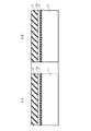
前記第1側面と前記第2側面の間隔は、前記上面から前記半導体基板側に向かうにつれて狭くなり、
前記第1突出部は、前記第1素子分離構造の上面と側面とをつなぐ第1傾斜面を有し、
前記第2突出部は、前記第2素子分離構造の上面と側面とをつなぐ第2傾斜面を有し、
前記第1傾斜面と前記第2傾斜面は対向しており、前記第1傾斜面と前記第2傾斜面の間隔は前記半導体基板から離れるにつれて広くなり、
前記フローティングゲートは、前記第1突出部と前記第2突出部に挟まれており、前記第1側面及び前記第2側面は前記第1傾斜面及び前記第2傾斜面のそれぞれと接触する
不揮発性半導体記憶装置。A semiconductor substrate;
A control gate and a floating gate formed side by side on a gate insulating film on a channel region in the semiconductor substrate;
An erase gate facing the top surface of the floating gate;
A first element isolation structure having a first protrusion protruding from the semiconductor substrate;
A second element isolation structure having a second protrusion protruding from the semiconductor substrate ,
The side surface of the floating gate includes a first side surface and a second side surface facing each other,
Distance between the second side and the first side,Ri narrowly toward from said upper surface to said semiconductorsubstrate,
The first protrusion has a first inclined surface that connects an upper surface and a side surface of the first element isolation structure,
The second protrusion has a second inclined surface that connects an upper surface and a side surface of the second element isolation structure,
The first inclined surface and the second inclined surface are opposed to each other, and an interval between the first inclined surface and the second inclined surface becomes wider as the distance from the semiconductor substrate increases.
The floating gate is sandwiched between the first protrusion and the second protrusion, and the first side surface and the second side surface are in contact with the first inclined surface and the second inclined surface, respectively . Semiconductor memory device.
前記フローティングゲートの前記上面は、第1辺において前記第1側面とつながり、第2辺において前記第2側面とつながり、
前記第1辺及び前記第2辺は、前記第1辺と前記第2辺との間の前記上面よりも上に位置する
不揮発性半導体記憶装置。The nonvolatile semiconductor memory device according to claim 1,
The upper surface of the floating gate is connected to the first side surface at a first side, and is connected to the second side surface at a second side,
The non-volatile semiconductor memory device, wherein the first side and the second side are located above the upper surface between the first side and the second side.
前記コントロールゲートと前記フローティングゲートは、前記チャネル領域上の前記ゲート絶縁膜上において第1方向に並んでおり、The control gate and the floating gate are arranged in a first direction on the gate insulating film on the channel region,
前記第1素子分離構造と前記第2素子分離構造は、前記第1方向に延伸するように形成されているThe first element isolation structure and the second element isolation structure are formed to extend in the first direction.
不揮発性半導体記憶装置。Nonvolatile semiconductor memory device.
前記フローティングゲートは、前記第1側面及び前記第2側面のそれぞれと前記上面とによって形成される2つの鋭角部を有し、
前記フローティングゲート中の電子は、前記2つの鋭角部から前記消去ゲートに引き抜かれる
不揮発性半導体記憶装置。A non-volatile semiconductor memory device according to any one of claims 1 to 3,
The floating gate has two acute angle portions formed by each of the first side surface and the second side surface and the upper surface,
Electrons in the floating gate are extracted from the two acute angle portions to the erase gate.
(B)前記第1突出部と前記第2突出部のそれぞれの上端部をエッチングすることにより、前記第1素子分離構造の上面と側面とをつなぐ第1傾斜面と、前記第2素子分離構造の上面と側面とをつなぐ第2傾斜面を形成することと、
ここで、前記第1傾斜面と前記第2傾斜面は対向しており、前記第1傾斜面と前記第2傾斜面の間隔は前記半導体基板から離れるにつれて広くなり、
(C)前記半導体基板上の第1ゲート絶縁膜上に、前記第1突出部と前記第2突出部とに挟まれるフローティングゲートを形成することと、
ここで、前記フローティングゲートの両側面は前記第1傾斜面及び前記第2傾斜面のそれぞれと接触し、前記フローティングゲートの上面は消去ゲートと対向し、
(D)前記フローティングゲートと並ぶコントロールゲートを、前記半導体基板上の第2ゲート絶縁膜上に形成することと
を含む
不揮発性半導体記憶装置の製造方法。(A) forming a first element isolation structure and a second element isolation structure each having a first protrusion and a second protrusion protruding from the semiconductor substrate;
(B) A first inclined surface that connects an upper surface and a side surface of the first element isolation structure by etching each upper end of the first protrusion and the second protrusion, and the second element isolation structure Forming a second inclined surface connecting the upper surface and the side surface of
Here, the first inclined surface and the second inclined surface are opposed to each other, and an interval between the first inclined surface and the second inclined surface becomes wider as the distance from the semiconductor substrate increases.
(C) forming a floating gate sandwiched between the first protrusion and the second protrusion on the first gate insulating film on the semiconductor substrate;
Here, both side surfaces of the floating gate are in contact with each of the first inclined surface and the second inclined surface, and an upper surface of the floating gate is opposed to the erase gate,
(D) forming a control gate along with the floating gate on a second gate insulating film on the semiconductor substrate. A method for manufacturing a nonvolatile semiconductor memory device.
前記フローティングゲートの上面は、対向する第1辺及び第2辺のそれぞれにおいて前記両側面とつながり、
前記フローティングゲートは、前記第1辺及び前記第2辺が前記第1辺と前記第2辺との間の前記上面よりも上に位置するように形成される
不揮発性半導体記憶装置の製造方法。A method for manufacturing the nonvolatile semiconductor memory device according to claim5 ,
The upper surface of the floating gate is connected to the both side surfaces at each of the first side and the second side facing each other,
The method of manufacturing a nonvolatile semiconductor memory device, wherein the floating gate is formed such that the first side and the second side are located above the upper surface between the first side and the second side.
Priority Applications (2)
| Application Number | Priority Date | Filing Date | Title |
|---|---|---|---|
| JP2008028579AJP5190986B2 (en) | 2008-02-08 | 2008-02-08 | Nonvolatile semiconductor memory device and manufacturing method thereof |
| US12/320,890US20090200594A1 (en) | 2008-02-08 | 2009-02-06 | Nonvolatile semiconductor memory device and method of manufacturing the same |
Applications Claiming Priority (1)
| Application Number | Priority Date | Filing Date | Title |
|---|---|---|---|
| JP2008028579AJP5190986B2 (en) | 2008-02-08 | 2008-02-08 | Nonvolatile semiconductor memory device and manufacturing method thereof |
Publications (2)
| Publication Number | Publication Date |
|---|---|
| JP2009188292A JP2009188292A (en) | 2009-08-20 |
| JP5190986B2true JP5190986B2 (en) | 2013-04-24 |
Family
ID=40938162
Family Applications (1)
| Application Number | Title | Priority Date | Filing Date |
|---|---|---|---|
| JP2008028579AExpired - Fee RelatedJP5190986B2 (en) | 2008-02-08 | 2008-02-08 | Nonvolatile semiconductor memory device and manufacturing method thereof |
Country Status (2)
| Country | Link |
|---|---|
| US (1) | US20090200594A1 (en) |
| JP (1) | JP5190986B2 (en) |
Families Citing this family (2)
| Publication number | Priority date | Publication date | Assignee | Title |
|---|---|---|---|---|
| US9159842B1 (en)* | 2014-03-28 | 2015-10-13 | Taiwan Semiconductor Manufacturing Co., Ltd. | Embedded nonvolatile memory |
| CN107305892B (en)* | 2016-04-20 | 2020-10-02 | 硅存储技术公司 | Method of Forming Tri-Gate Non-Volatile Flash Memory Cell Pairs Using Two Polysilicon Deposition Steps |
Family Cites Families (11)
| Publication number | Priority date | Publication date | Assignee | Title |
|---|---|---|---|---|
| US6211547B1 (en)* | 1997-11-24 | 2001-04-03 | Winbond Electronics Corporation | Semiconductor memory array with buried drain lines and processing methods therefor |
| JP2001230330A (en)* | 2000-02-18 | 2001-08-24 | Sanyo Electric Co Ltd | Nonvolatile semiconductor memory and its manufacturing method |
| US6579761B1 (en)* | 2002-08-20 | 2003-06-17 | Taiwan Semiconductor Manufacturing Company | Method to improve the coupling ratio of top gate to floating gate in flash |
| JP3936315B2 (en)* | 2003-07-04 | 2007-06-27 | 株式会社東芝 | Semiconductor memory device and manufacturing method thereof |
| JP2006269814A (en)* | 2005-03-24 | 2006-10-05 | Toshiba Corp | Nonvolatile semiconductor memory device and manufacturing method thereof |
| TWI258207B (en)* | 2005-06-07 | 2006-07-11 | Powerchip Semiconductor Corp | Flash memory and manufacturing method thereof |
| US20070166903A1 (en)* | 2006-01-17 | 2007-07-19 | Bohumil Lojek | Semiconductor structures formed by stepperless manufacturing |
| US7508028B2 (en)* | 2006-10-26 | 2009-03-24 | Episil Technologies Inc. | Non-volatile memory |
| KR100789409B1 (en)* | 2007-01-02 | 2007-12-28 | 삼성전자주식회사 | Ypyrom element and its manufacturing method |
| US7736973B2 (en)* | 2008-01-25 | 2010-06-15 | Sandisk Corporation | Non-volatile memory arrays having dual control gate cell structures and a thick control gate dielectric and methods of forming |
| JP2009188293A (en)* | 2008-02-08 | 2009-08-20 | Nec Electronics Corp | Nonvolatile semiconductor memory device and manufacturing method thereof |
- 2008
- 2008-02-08JPJP2008028579Apatent/JP5190986B2/ennot_activeExpired - Fee Related
- 2009
- 2009-02-06USUS12/320,890patent/US20090200594A1/ennot_activeAbandoned
Also Published As
| Publication number | Publication date |
|---|---|
| US20090200594A1 (en) | 2009-08-13 |
| JP2009188292A (en) | 2009-08-20 |
Similar Documents
| Publication | Publication Date | Title |
|---|---|---|
| JP5503843B2 (en) | Nonvolatile semiconductor memory device and manufacturing method thereof | |
| JP5190985B2 (en) | Nonvolatile semiconductor memory device and manufacturing method thereof | |
| JP2009188293A (en) | Nonvolatile semiconductor memory device and manufacturing method thereof | |
| JP5191633B2 (en) | Semiconductor device and manufacturing method thereof | |
| JP3976729B2 (en) | Memory cell, memory cell configuration, and manufacturing method | |
| TWI244200B (en) | Flash memory with trench select gate and fabrication process | |
| JP3966707B2 (en) | Semiconductor device and manufacturing method thereof | |
| US9231115B2 (en) | Semiconductor device and manufacturing method thereof | |
| JP5781733B2 (en) | Nonvolatile memory cell and manufacturing method thereof | |
| US6168994B1 (en) | Method of making memory device with an element splitting trench | |
| JP2003332469A (en) | Nonvolatile semiconductor memory device and method of manufacturing the same | |
| JP2008251825A (en) | Manufacturing method of semiconductor memory device | |
| JP5106022B2 (en) | Nonvolatile semiconductor memory device and manufacturing method thereof | |
| JP2009088060A (en) | Nonvolatile semiconductor memory device and manufacturing method thereof | |
| JP2009194106A (en) | Nonvolatile semiconductor memory device and method for manufacturing nonvolatile semiconductor memory device | |
| CN107871725A (en) | Semiconductor device and manufacturing method thereof | |
| US11094833B2 (en) | Semiconductor device including memory using hafnium and a method of manufacturing the same | |
| JP2009016615A (en) | Semiconductor memory device | |
| JP5998512B2 (en) | Semiconductor device and manufacturing method of semiconductor device | |
| US10163922B2 (en) | Semiconductor device and method of manufacturing the semiconductor device | |
| US20070170494A1 (en) | Nonvolatile memory device and method for fabricating the same | |
| JP4557678B2 (en) | Semiconductor memory device | |
| JP5190986B2 (en) | Nonvolatile semiconductor memory device and manufacturing method thereof | |
| JP2009289949A (en) | Nonvolatile semiconductor memory device | |
| KR100732629B1 (en) | Nonvolatile Memory Device and Formation Method |
Legal Events
| Date | Code | Title | Description |
|---|---|---|---|
| A621 | Written request for application examination | Free format text:JAPANESE INTERMEDIATE CODE: A621 Effective date:20100811 | |
| A131 | Notification of reasons for refusal | Free format text:JAPANESE INTERMEDIATE CODE: A131 Effective date:20121113 | |
| A521 | Request for written amendment filed | Free format text:JAPANESE INTERMEDIATE CODE: A523 Effective date:20130107 | |
| TRDD | Decision of grant or rejection written | ||
| A01 | Written decision to grant a patent or to grant a registration (utility model) | Free format text:JAPANESE INTERMEDIATE CODE: A01 Effective date:20130123 | |
| A61 | First payment of annual fees (during grant procedure) | Free format text:JAPANESE INTERMEDIATE CODE: A61 Effective date:20130125 | |
| R150 | Certificate of patent or registration of utility model | Free format text:JAPANESE INTERMEDIATE CODE: R150 | |
| FPAY | Renewal fee payment (event date is renewal date of database) | Free format text:PAYMENT UNTIL: 20160208 Year of fee payment:3 | |
| S531 | Written request for registration of change of domicile | Free format text:JAPANESE INTERMEDIATE CODE: R313531 | |
| R350 | Written notification of registration of transfer | Free format text:JAPANESE INTERMEDIATE CODE: R350 | |
| LAPS | Cancellation because of no payment of annual fees |