JP5176428B2 - Oxynitriding apparatus and method, and semiconductor device manufacturing method - Google Patents
Oxynitriding apparatus and method, and semiconductor device manufacturing methodDownload PDFInfo
- Publication number
- JP5176428B2 JP5176428B2JP2007213924AJP2007213924AJP5176428B2JP 5176428 B2JP5176428 B2JP 5176428B2JP 2007213924 AJP2007213924 AJP 2007213924AJP 2007213924 AJP2007213924 AJP 2007213924AJP 5176428 B2JP5176428 B2JP 5176428B2
- Authority
- JP
- Japan
- Prior art keywords
- oxynitriding
- gas
- concentration
- processing
- film
- Prior art date
- Legal status (The legal status is an assumption and is not a legal conclusion. Google has not performed a legal analysis and makes no representation as to the accuracy of the status listed.)
- Expired - Fee Related
Links
Images


Landscapes
- Metal-Oxide And Bipolar Metal-Oxide Semiconductor Integrated Circuits (AREA)
- Formation Of Insulating Films (AREA)
- Semiconductor Memories (AREA)
- Non-Volatile Memory (AREA)
- Insulated Gate Type Field-Effect Transistor (AREA)
Description
Translated fromJapanese本発明は、NOガスを含む処理ガスを用いた酸窒化処理を行う酸窒化処理装置及び方法、及び半導体基板の表面又は前記半導体基板の上方に形成された薄膜(ゲート絶縁膜、キャパシタ絶縁膜、トンネル絶縁膜等)にNOガスを含む処理ガスを用いた酸窒化処理を行う半導体装置の製造方法に関する。 The present invention relates to an oxynitriding apparatus and method for performing oxynitriding using a processing gas containing NO gas, and a thin film (a gate insulating film, a capacitor insulating film, a film formed on the surface of a semiconductor substrate or above the semiconductor substrate) The present invention relates to a method for manufacturing a semiconductor device that performs oxynitriding using a processing gas containing NO gas on a tunnel insulating film or the like.
半導体集積回路装置では、その集積度及び動作速度を向上させるためには、構成要素であるMISFETを小型化し、ゲート絶縁膜を薄膜化する必要がある。ゲート絶縁膜上に形成されるゲート電極は通常、ポリシリコン層、又はポリシリコン層とシリサイド層の積層で形成される。ポリシリコン層は、通常ソース/ドレイン領域と同時に不純物をイオン注入される。表面チャネル型nチャネルMISFETのゲート電極、ソース/ドレイン領域にはn型不純物がイオン注入される。表面チャネル型pチャネルMISFETのゲート電極、ソース/ドレイン領域にはp型不純物がイオン注入される。 In a semiconductor integrated circuit device, in order to improve the degree of integration and the operation speed, it is necessary to reduce the size of the MISFET that is a component and reduce the thickness of the gate insulating film. The gate electrode formed on the gate insulating film is usually formed of a polysilicon layer or a stacked layer of a polysilicon layer and a silicide layer. The polysilicon layer is usually ion-implanted with impurities simultaneously with the source / drain regions. An n-type impurity is ion-implanted into the gate electrode and source / drain regions of the surface channel n-channel MISFET. A p-type impurity is ion-implanted into the gate electrode and source / drain regions of the surface channel p-channel MISFET.
ゲート絶縁膜を薄く形成すると、表面チャネル型pチャネルMISFETのゲート電極にイオン注入したp型不純物(例えばホウ素(B))ゲート絶縁膜を突き抜け、チャネル領域に達してしまう現象が生じる。n型領域であるチャネル領域にp型不純物が浸透することにより、閾値を変動させるのみでなく、移動度が劣化する。
更に、ゲート絶縁膜を薄膜化により、ゲート電極とチャネル領域との間にトンネル電流が流れ、ゲートリーク電流が増加するという問題も発生する。ゲート絶縁膜を約0.2nm薄くすることでゲートリーク電流が一桁増加することが知られている。When the gate insulating film is thinly formed, a phenomenon occurs that a p-type impurity (for example, boron (B)) ion-implanted into the gate electrode of the surface channel p-channel MISFET penetrates the gate insulating film and reaches the channel region. The penetration of p-type impurities into the channel region, which is an n-type region, not only changes the threshold value but also degrades mobility.
Further, the thinning of the gate insulating film causes a problem that a tunnel current flows between the gate electrode and the channel region, and the gate leakage current increases. It is known that the gate leakage current increases by an order of magnitude by making the gate insulating film about 0.2 nm thin.
上記したp型不純物の突き抜け現象を抑制するには、シリコン酸化膜であるゲート絶縁膜に窒素を導入し、シリコン酸窒化膜とすることが有効である。シリコン酸化膜中へ窒素を導入するには、NH3ガス、NOガス、N2Oガス等の窒化性ガス雰囲気中で、抵抗加熱やランプ加熱によりシリコン基板を加熱する方法がある。また、例えば窒素プラズマを用い、シリコン酸化膜中に高濃度の窒素を導入する方法も知られている。In order to suppress the above-described phenomenon of p-type impurity penetration, it is effective to introduce nitrogen into the gate insulating film, which is a silicon oxide film, to form a silicon oxynitride film. In order to introduce nitrogen into the silicon oxide film, there is a method in which the silicon substrate is heated by resistance heating or lamp heating in a nitride gas atmosphere such as NH3 gas, NO gas, or N2 O gas. Also known is a method of introducing a high concentration of nitrogen into a silicon oxide film using, for example, nitrogen plasma.
更に、ゲート絶縁膜を、一般的にシリコン酸化物よりも誘電率の高いシリコン酸窒化物等の高誘電率絶縁物により形成することにより、反転容量換算膜厚を薄く抑えつつ、物理的膜厚を厚くし、ゲートリーク電流の発生を抑制することができる。 Furthermore, the gate insulating film is generally formed of a high dielectric constant insulator such as silicon oxynitride having a dielectric constant higher than that of silicon oxide. The gate leakage current can be suppressed from being increased.
高誘電率絶縁膜であるシリコン酸窒化膜を形成するには、NO(一酸化窒素)ガスを処理ガスとして用いて酸窒化処理を行う。この場合、予め形成されたシリコン酸化膜を上記のように窒化する手法と、直接的にシリコン酸窒化膜を形成する手法とがある。
前者の手法の一例として、特許文献1では、シリコン酸化膜を酸化窒素雰囲気で熱処理し窒化する際に、圧力(数torrから常圧)及び処理温度を調整するとしている。酸化窒素としては、NO,N2O,NO2等を挙げられ、これらは混合して用いても良く、中でもNOが好ましい。またN2やAr,He等の不活性ガスとの混合ガスであっても良いとしている。
同様に、特許文献2では、760torrの圧力以下でNO又はN2Oガスを炉中へ注入してシリコン酸化膜を窒化するとしている。また、NOガスの処理圧力を数torrから常圧まで変化させることにより、同一温度及び同一時間の処理を行った際に、膜厚や膜中の窒素濃度が異なることが示されている。In order to form a silicon oxynitride film which is a high dielectric constant insulating film, an oxynitride process is performed using NO (nitrogen monoxide) gas as a process gas. In this case, there are a method of nitriding a previously formed silicon oxide film as described above and a method of directly forming a silicon oxynitride film.
As an example of the former method, in
Similarly, in
一方、後者の手法の一例として、特許文献3では、シリコン基板をNOガス雰囲気で熱処理することによりシリコン酸窒化膜を形成する際に同時に、一酸化炭素ガス等の還元性ガスを添加することにより、膜中の窒素濃度を増加させることができるとしている。 On the other hand, as an example of the latter method, in
近時では、ゲート絶縁膜の薄膜化の要請が益々高まっており、膜厚2nm以下のゲート絶縁膜が検討されている。この程度までゲート絶縁膜の薄膜化を進める場合、その材料にシリコン酸窒化物を用いたとしても、ゲートリーク電流を抑制することが困難となる。ゲートリーク電流を十分に抑制するには、ゲート絶縁膜の膜厚、及び膜中の窒素濃度を適宜制御することが必要となる。ゲート絶縁膜のシリコン基板との界面における窒素濃度の制御は、チャネル領域における移動度の低下、ストレスをかけて温度を上昇させた時の劣化特性であるNBTI(Negative Bias Temperature Instability)特性の劣化に大きく関与する。 Recently, there is an increasing demand for a thinner gate insulating film, and a gate insulating film having a thickness of 2 nm or less is being studied. When the gate insulating film is made thinner to this extent, it is difficult to suppress the gate leakage current even if silicon oxynitride is used as the material. In order to sufficiently suppress the gate leakage current, it is necessary to appropriately control the thickness of the gate insulating film and the nitrogen concentration in the film. Control of the nitrogen concentration at the interface between the gate insulating film and the silicon substrate is caused by a decrease in mobility in the channel region and deterioration of NBTI (Negative Bias Temperature Instability) characteristics, which is a deterioration characteristic when the temperature is increased by applying stress. Greatly involved.
ここで、膜厚2nm以下のような極薄のゲート絶縁膜を形成する場合、酸窒化処理の処理ガスであるNOガスの状態が、形成されるゲート絶縁膜に与える影響を無視できなくなる懸念がある。しかしながら、例えば既述の特許文献1では、シリコン酸窒化膜の膜厚が窒素濃度で変化する旨が、特許文献2では、シリコン酸窒化膜の膜厚がNOガスの処理圧力で変化する旨が確認されているのみであり、現在のところ、シリコン酸窒化物からなる極薄のゲート絶縁膜を形成する際に、酸窒化処理の処理ガスにおける如何なる因子が影響を与えるかについての詳細な検討はなされていない。 Here, when an extremely thin gate insulating film having a thickness of 2 nm or less is formed, there is a concern that the influence of the state of NO gas, which is a processing gas for oxynitriding, on the formed gate insulating film cannot be ignored. is there. However, for example, in
本発明は、上記の課題に鑑みてなされたものであり、NOガスを処理ガスとして用いた酸窒化処理を行うに際して、当該酸窒化処理により所望の膜厚及び窒素濃度の薄膜を得ることを可能とする酸窒化処理装置及び方法、及びこの酸窒化処理方法を適用して、高集積化及び微細化の要請に応える信頼性の高い半導体装置を実現する半導体装置の製造方法を提供することを目的とする。 The present invention has been made in view of the above problems. When performing oxynitriding using NO gas as a processing gas, it is possible to obtain a thin film having a desired film thickness and nitrogen concentration by the oxynitriding. An object of the present invention is to provide an oxynitriding apparatus and method, and a semiconductor device manufacturing method that realizes a highly reliable semiconductor device that meets the demand for higher integration and miniaturization by applying the oxynitriding process. And
本発明の酸窒化処理方法は、NOガスを処理ガスとして用いた酸窒化処理を行うに際して、前記処理ガス中に存在し、前記処理ガス中で自己分解により増加するNxOy組成(0<x≦2,0<y≦2,x≠y)の1種又は複数種の不純物の濃度を計測する第1の工程と、前記酸窒化処理により生成される酸窒化膜の膜厚又は前記酸窒化膜の窒素濃度が所定範囲内の値となるように、前記第1の工程で計測された前記不純物の濃度に応じて前記酸窒化処理を行う第2の工程とを含む。In the oxynitriding method of the present invention, when an oxynitriding process using NO gas as a processing gas is performed, the Nx Oy composition (0 < a first step of measuring the concentration of one or a plurality of impurities of x ≦ 2, 0 <y ≦ 2, x ≠ y), and the thickness of the oxynitride film generated by the oxynitriding treatment or the acid And a second step of performing the oxynitriding process in accordance with the impurity concentration measured in the first step so that the nitrogen concentration of the nitride film becomes a value within a predetermined range.
本発明の酸窒化処理方法は、NOガスを処理ガスとして用いた酸窒化処理を行うに際して、前記処理ガス中に存在し、前記処理ガス中で自己分解により増加するNxOy組成(0<x≦2,0<y≦2,x≠y)の1種又は複数種の不純物の濃度を計測する第1の工程と、前記第1の工程で計測された前記不純物の濃度が所定範囲内の値である場合に、前記酸窒化処理を行う第2の工程とを含む。In the oxynitriding method of the present invention, when an oxynitriding process using NO gas as a processing gas is performed, the Nx Oy composition (0 < a first step of measuring the concentration of one or more impurities of x ≦ 2, 0 <y ≦ 2, x ≠ y), and the concentration of the impurity measured in the first step is within a predetermined range And the second step of performing the oxynitriding treatment.
本発明の酸窒化処理装置は、NOガスを処理ガスとして用いた酸窒化処理を行う酸窒化処理装置であって、被処理体を収容する処理チャンバーと、前記処理ガスに存在し、前記処理ガス中で自己分解により増加するNxOy組成(0<x≦2,0<y≦2,x≠y)の1種又は複数種の不純物の濃度を計測する濃度計測部と、前記濃度計測部で計測された前記不純物の濃度に応じて、前記酸窒化処理により生成される酸窒化膜の膜厚又は前記酸窒化膜の窒素濃度が所定範囲内の値となるように、前記酸窒化処理における処理圧力を算出する圧力算出部と、前記処理ガス中で自己分解により増加するNxOy組成(0<x≦2,0<y≦2,x≠y)の1種又は複数種の前記不純物の濃度と、前記酸窒化処理により形成される前記酸窒化膜の膜厚又は前記酸窒化膜の窒素濃度と、前記酸窒化処理時における前記処理チャンバ―内の圧力との相関関係の諸データを記録する記録部とを含む。The oxynitriding apparatus of the present invention is an oxynitriding apparatus that performs oxynitriding using NO gas as a processing gas, and is present in a processing chamber that accommodates an object to be processed, the processing gas, and the processing gas A concentration measuring unit for measuring the concentration of one or a plurality of impurities having an Nx Oy composition (0 <x ≦ 2, 0 <y ≦ 2, x ≠ y) that increases by self-decomposition, and the concentration measurement The oxynitridation treatment is performed so that the thickness of the oxynitride film generated by the oxynitridation treatment or the nitrogen concentration of the oxynitride film becomes a value within a predetermined range according to the concentration of the impurity measured in the section A pressure calculation unit for calculating a processing pressure in theprocess gas, andone or a plurality of types ofNxOycomposition (0 <x ≦ 2, 0 <y ≦ 2, x ≠ y)increased by self-decomposition in the processing gasThe concentration of the impurity and the thickness of the oxynitride film formed by the oxynitriding process Or a recording unit for recording various data on the correlation between the nitrogen concentration of the oxynitride film and the pressure in the processing chamber during the oxynitriding process .
本発明の半導体装置の製造方法は、半導体基板の表面又は前記半導体基板の上方に形成された酸窒化膜を有する半導体装置の製造方法であって、前記酸窒化膜に、NOガスを処理ガスとして用いた酸窒化処理を行うに際して、前記処理ガス中に存在し、前記処理ガス中で自己分解により増加するNxOy組成(0<x≦2,0<y≦2,x≠y)の1種又は複数種の不純物の濃度を計測する第1の工程と、前記酸窒化処理により生成される前記酸窒化膜の膜厚又は前記酸窒化膜の窒素濃度が所定範囲内の値となるように、前記第1の工程で計測された前記不純物の濃度に応じて前記酸窒化処理を行う第2の工程とを含む。A method of manufacturing a semiconductor device according to the present invention is a method of manufacturing a semiconductor device having an oxynitride film formed on a surface of a semiconductor substrate or above the semiconductor substrate, and NO gas is used as a processing gas for the oxynitride film. When performing the oxynitriding treatment used, the Nx Oy composition (0 <x ≦ 2, 0 <y ≦ 2, x ≠ y) that exists in the processing gas and increases by self-decomposition in the processing gas. The first step of measuring the concentration of one or more types of impurities, and the film thickness of the oxynitride film generated by the oxynitriding process or the nitrogen concentration of the oxynitride film is a value within a predetermined range. And a second step of performing the oxynitridation treatment in accordance with the concentration of the impurity measured in the first step.
本発明の半導体装置の製造方法は、半導体基板の表面又は前記半導体基板の上方に形成された酸窒化膜を有する半導体装置の製造方法であって、前記酸窒化膜に、NOガスを処理ガスとして用いた酸窒化処理を行うに際して、前記処理ガス中に存在し、前記処理ガス中で自己分解により増加するNxOy組成(0<x≦2,0<y≦2,x≠y)の1種又は複数種の不純物の濃度を計測する第1の工程と、前記第1の工程で計測された前記不純物の濃度が所定範囲内の値である場合に、前記酸窒化処理を行う第2の工程とを含む。A method of manufacturing a semiconductor device according to the present invention is a method of manufacturing a semiconductor device having an oxynitride film formed on a surface of a semiconductor substrate or above the semiconductor substrate, and NO gas is used as a processing gas for the oxynitride film. When performing the oxynitriding treatment used, the Nx Oy composition (0 <x ≦ 2, 0 <y ≦ 2, x ≠ y) that exists in the processing gas and increases by self-decomposition in the processing gas. A first step of measuring the concentration of one or a plurality of types of impurities, and a second step of performing the oxynitriding treatment when the concentration of the impurities measured in the first step is a value within a predetermined range. These steps are included.
本発明によれば、NOガスを処理ガスとして用いた酸窒化処理を行うに際して、当該酸窒化処理により所望の膜厚及び窒素濃度の薄膜を得ることが可能となる。また、当該酸窒化処理を半導体装置の製造に適用することにより、高集積化及び微細化の要請に応える信頼性の高い半導体装置が実現する。 According to the present invention, when performing an oxynitriding process using NO gas as a processing gas, a thin film having a desired film thickness and nitrogen concentration can be obtained by the oxynitriding process. In addition, by applying the oxynitridation treatment to the manufacture of a semiconductor device, a highly reliable semiconductor device that meets the demand for high integration and miniaturization can be realized.
−本発明の基本骨子−
本発明者は、NOガスを処理ガスとして用いた酸窒化処理により、シリコン酸窒化物からなる膜厚2nm以下の酸窒化膜を形成する際に、酸窒化処理の処理ガスの当該酸窒化膜に比較的大きな影響を与える因子が、処理ガス中に存在し、処理ガス中で自己分解により増加するNxOy組成(0<x≦2,0<y≦2,x≠y)の1種又は複数種の不純物(NO2,N2O等)の濃度であることを見出した。-Basic outline of the present invention-
The present inventor, when forming an oxynitride film made of silicon oxynitride with a film thickness of 2 nm or less by oxynitriding using NO gas as a processing gas, A factor having a relatively large influence exists in the processing gas, and is a kind of Nx Oy composition (0 <x ≦ 2, 0 <y ≦ 2, x ≠ y) that increases by self-decomposition in the processing gas. or found to be concentration of a plurality of types of impurities (NO2, N2 O, etc.).
本発明では、この事実に基づき、酸窒化処理を行うに際して、処理ガスの不純物濃度を計測し、生成される酸窒化膜の膜厚又は酸窒化膜の窒素濃度が所定範囲内の値となるように、計測された不純物濃度に応じて当該酸窒化処理を行う。ここで、詳細には、処理ガス中の不純物濃度と、形成される酸窒化膜の膜厚又は窒素濃度との相関関係を予め計測し規定しておく。そして、当該相関関係に基づき、膜厚又は窒素濃度が所定範囲内の値となるように、計測された不純物濃度に応じて、具体的には酸窒化処理における処理圧力(処理チャンバー内における酸窒化処理の圧力)を調節設定して当該処理を行う。この処理圧力についても同様に、当該処理圧力と膜厚又は窒素濃度との相関関係を予め計測し規定しておき、当該相関関係に基づいて膜厚及び窒素濃度が所定範囲内の値となるように処理圧力を設定する。 In the present invention, based on this fact, when the oxynitriding process is performed, the impurity concentration of the processing gas is measured so that the thickness of the generated oxynitride film or the nitrogen concentration of the oxynitride film becomes a value within a predetermined range. In addition, the oxynitriding process is performed in accordance with the measured impurity concentration. Here, in detail, the correlation between the impurity concentration in the processing gas and the film thickness or nitrogen concentration of the formed oxynitride film is measured and defined in advance. Then, based on the measured impurity concentration so that the film thickness or nitrogen concentration becomes a value within a predetermined range based on the correlation, specifically, the processing pressure in oxynitriding (oxynitriding in the processing chamber) The processing is performed by adjusting and setting the processing pressure. Similarly, for this processing pressure, the correlation between the processing pressure and the film thickness or nitrogen concentration is measured and defined in advance, and the film thickness and nitrogen concentration are set to values within a predetermined range based on the correlation. Set the processing pressure to.
この構成により、酸窒化処理を行う(処理ガスを用いる)ときに、処理ガスが自己分解により当初と異なる不純物濃度となった場合でも、当該処理ガスの不純物濃度を測定し、上記した各相関関係に基づいて処理圧力を設定するのみで、膜厚又は窒素濃度が所定範囲内とされた所期の酸窒化膜を容易且つ確実に形成することができる。 With this configuration, when an oxynitriding process is performed (using a processing gas), even if the processing gas has an impurity concentration different from the original due to self-decomposition, the impurity concentration of the processing gas is measured, and each of the correlations described above The desired oxynitride film whose film thickness or nitrogen concentration is within a predetermined range can be easily and reliably formed only by setting the processing pressure based on the above.
また、酸窒化処理に用いる処理ガスとして、例えば99.99%に高純度に精製されたNOガスを処理ガスとして用いる場合、計測された各不純物濃度がそれぞれ所定範囲内の値、例えば30ppm以下であれば、上記の処理圧力の設定をすることなくそのままの状態で酸窒化処理を行う。 In addition, when NO gas purified to a high purity of 99.99%, for example, is used as a processing gas as a processing gas used for the oxynitriding process, each measured impurity concentration is a value within a predetermined range, for example, 30 ppm or less. If there is, the oxynitriding process is performed as it is without setting the above processing pressure.
ここで、処理ガスにおける不純物濃度の管理の容易性等を考慮して、各不純物濃度の合計を基準値としても好適である。即ちこの場合、計測された各不純物濃度の合計が所定範囲内の値、例えば60ppm以下であれば、上記の処理圧力の設定をすることなくそのままの状態で酸窒化処理を行う。 Here, considering the ease of management of the impurity concentration in the processing gas, the total of each impurity concentration is also preferable as the reference value. That is, in this case, if the total of the measured impurity concentrations is within a predetermined range, for example, 60 ppm or less, the oxynitriding process is performed as it is without setting the above processing pressure.
この構成により、当該処理ガスの不純物濃度を測定し、各不純物濃度がそれぞれ所定範囲内、例えば30ppm以下(或いは、各不純物濃度の合計が所定範囲内、例えば60ppm以下)であることを確認するだけで、処理圧力の設定の何等の調節も行うことなく、膜厚又は窒素濃度が所定範囲内とされた所期の酸窒化膜を容易且つ確実に形成することができる。 With this configuration, it is only necessary to measure the impurity concentration of the processing gas and confirm that each impurity concentration is within a predetermined range, for example, 30 ppm or less (or the total of the impurity concentrations is within a predetermined range, for example, 60 ppm or less). Thus, the desired oxynitride film in which the film thickness or the nitrogen concentration is within a predetermined range can be easily and reliably formed without any adjustment of the setting of the processing pressure.
ここで、処理ガスの不純物濃度を測定した結果、その値が所定範囲を逸脱する場合には、上記した各相関関係に基づいて処理圧力を設定して酸窒化処理を行えば良い。勿論、不純物濃度が所定範囲を逸脱する場合には、当該処理ガス(が封止されたガスボンベ)を廃棄しても良いし、当該処理ガスがこの状態となるまでに、できるだけそのガスボンベを使い切るように、プロセスを設定しても好適である。 Here, as a result of measuring the impurity concentration of the processing gas, if the value deviates from the predetermined range, the processing pressure may be set based on each of the above correlations to perform the oxynitriding process. Of course, when the impurity concentration deviates from the predetermined range, the processing gas (gas cylinder sealed) may be discarded, or the gas cylinder may be used up as much as possible before the processing gas is in this state. It is also preferable to set a process.
−本発明を適用した具体的な諸実施形態−
以下、本発明を適用した具体的な諸実施形態について、図面を参照しながら詳細に説明する。-Specific embodiments to which the present invention is applied-
Hereinafter, specific embodiments to which the present invention is applied will be described in detail with reference to the drawings.
[第1の実施形態]
本実施形態では、本発明を適用した、NOガスを処理ガスとして用いる酸窒化処理を開示する。
(本実施形態による酸窒化処理の経緯)
(1)酸窒化処理において、処理ガス中の不純物濃度と、形成されたシリコン酸窒化膜の膜厚との相関関係について
本発明者は、シリコン基板の表面に、NOガスの雰囲気下で酸窒化処理を施して形成したシリコン酸窒化膜について、その膜厚を約3ヶ月超の期間に亘り80回以上調査した。その結果、酸素(O2)ガスの雰囲気下で形成したシリコン酸化膜に比べて、安定性に欠けることが明らかとなった。以下、この経緯について、図1及び図2を用いて説明する。[First Embodiment]
In the present embodiment, an oxynitriding process using NO gas as a processing gas to which the present invention is applied is disclosed.
(Background of the oxynitriding process according to this embodiment)
(1) In the oxynitridation process, the correlation between the impurity concentration in the process gas and the film thickness of the formed silicon oxynitride film is as follows. The silicon oxynitride film formed by the treatment was investigated 80 times or more over a period of about 3 months. As a result, it was revealed that the film lacks stability compared to a silicon oxide film formed in an oxygen (O2 ) gas atmosphere. Hereinafter, this process will be described with reference to FIGS.
通常、NOガスを処理ガスとして用いる酸窒化処理において、処理ガスは、そのNOガスの純度は99.9%未満であり、更に1000ppm未満のN2,NO2,N2Oや、数ppmのH2O等の不純物を含有した状態でガスボンベ(以下、NOガスボンベと記す。)等に充填されている。Usually, in the oxynitriding process using NO gas as a processing gas, the processing gas has a purity of NO gas of less than 99.9%, and further less than 1000 ppm of N2 , NO2 , N2 O, several ppm A gas cylinder (hereinafter referred to as an NO gas cylinder) or the like is filled with impurities such as H2 O.
表1に、シリコン基板をO2ガスの雰囲気下で酸化処理してシリコン酸化膜を形成した場合と、シリコン基板をNOガスの雰囲気下で酸窒化処理してシリコン酸窒化膜を形成した場合とについて、それぞれ膜厚を測定した結果を示す。前記の処理を各々、80回以上実施した平均の膜厚と、その標準偏差とをまとめて記載する。ここでは、急速ランプ加熱処理装置を用い、酸化処理は処理温度900℃、処理圧力6.7×10²Pa(5torr)の条件で行い、酸窒化処理は処理温度950℃、処理圧力6.7×10²Pa(5torr)の条件で行った。膜厚測定には、エリプソメータを用い、屈折率nとして、n=1.462のシリコン酸化膜の値を用いた。酸化処理では、標準偏差が0.780%であったのに対して、酸窒化処理では1.261%となった。このように、酸窒化処理では酸化処理に比べて、形成される薄膜の膜厚にばらつきが見られる。Table 1 shows a case where a silicon substrate is oxidized in an O2 gas atmosphere to form a silicon oxide film, and a case where a silicon substrate is subjected to an oxynitriding process in an NO gas atmosphere to form a silicon oxynitride film. About each, the result of having measured the film thickness is shown. The average film thickness and the standard deviation of each of the above treatments performed 80 times or more are collectively described. Here, a rapid lamp heat treatment apparatus is used, the oxidation treatment is performed under conditions of a treatment temperature of 900 ° C. and a treatment pressure of 6.7 × 10² Pa (5 torr), and the oxynitriding treatment is carried out at a treatment temperature of 950 ° C. and a treatment pressure of 6.7. The test was performed under the conditions of × 102 Pa (5 torr). For the film thickness measurement, an ellipsometer was used, and the value of the silicon oxide film with n = 1.462 was used as the refractive index n. In the oxidation treatment, the standard deviation was 0.780%, whereas in the oxynitriding treatment, it was 1.261%. As described above, in the oxynitriding process, the thickness of the formed thin film varies as compared with the oxidizing process.

図1は、10月8日〜11月5日に亘り、シリコン基板の表面に、NOガスを処理ガスとして用いた酸窒化処理により形成したシリコン酸窒化膜の膜厚及び不純物濃度を示す特性図である。ここで、横軸が調査月日、縦軸では左軸が膜厚を、右軸がNOガス中の不純物濃度の出荷分析値を示す。
破線で示す10月24日〜10月30日の間では、NOガスボンベを交換しており、この交換直後にシリコン酸窒化膜の膜厚が約0.02nm薄く変化した。製造時期の異なるNOガスボンベを用いたところ、処理温度、処理圧力、ガス流量、及び処理時間等のプロセス条件が全く同一でも、膜厚の変化が確認される。同様に、膜厚低下を招いたNOガスボンベを用いた期間に、不純物であるNO2,N2Oの低下を確認した。その後、10月24日以前のNOガスボンベに戻して酸窒化処理を行ったところ、膜厚及び不純物濃度は共にNOガスボンベの交換前の状態に回復した。以上から、酸窒化処理により形成されるシリコン酸窒化膜の膜厚は、処理ガスであるNOガス中に存在するNO2,N2Oの不純物含有量と強い相関関係があることが判る。FIG. 1 is a characteristic diagram showing the thickness and impurity concentration of a silicon oxynitride film formed by oxynitriding using NO gas as a processing gas on the surface of a silicon substrate from October 8 to November 5. It is. Here, the horizontal axis indicates the survey date, the vertical axis indicates the film thickness, and the right axis indicates the shipping analysis value of the impurity concentration in the NO gas.
The NO gas cylinder was exchanged between October 24 and October 30 indicated by the broken line, and immediately after the exchange, the film thickness of the silicon oxynitride film was thinned by about 0.02 nm. When NO gas cylinders having different production times are used, even if the process conditions such as the processing temperature, the processing pressure, the gas flow rate, and the processing time are exactly the same, a change in the film thickness is confirmed. Similarly, it was confirmed that NO2 and N2 O, which are impurities, were reduced during the period using the NO gas cylinder that caused the film thickness reduction. After that, when the oxynitriding process was performed by returning to the NO gas cylinder before October 24, both the film thickness and the impurity concentration were restored to the state before the replacement of the NO gas cylinder. From the above, it can be seen that the film thickness of the silicon oxynitride film formed by the oxynitriding process has a strong correlation with the impurity contents of NO2 and N2 O present in the NO gas that is the processing gas.
更に、図1でNOガスボンベを交換する前の比較的長期間について、シリコン酸窒化膜の膜厚及び不純物濃度について調べた。
図2は、7月22日〜11月5日に亘り、シリコン基板の表面に、NOガスを処理ガスとして用いた酸窒化処理により形成したシリコン酸窒化膜の膜厚及び不純物濃度を示す特性図である。ここで、横軸が調査月日、縦軸では左軸が膜厚を、右軸が不純物濃度の出荷分析値を示す。Further, the film thickness and impurity concentration of the silicon oxynitride film were examined for a relatively long period before replacing the NO gas cylinder in FIG.
FIG. 2 is a characteristic diagram showing the film thickness and impurity concentration of a silicon oxynitride film formed by oxynitriding using NO gas as a processing gas on the surface of a silicon substrate from July 22 to November 5. It is. Here, the horizontal axis indicates the survey date, the vertical axis indicates the film thickness, and the right axis indicates the shipping analysis value of the impurity concentration.
図1と同様に、破線で示す10月24日〜10月30日の間でNOガスボンベを交換しており、交換前には図1と同一製造ロットのNOガスボンベを使用している。ここで、7月22日〜10月24日の間では、徐々に膜厚の増加傾向が確認される。図中の縦軸の右軸に記したNOガス中の不純物濃度は飽くまでも製造時のものであり、酸窒化処理の実施日における濃度ではない。上記のガスボンベ交換による影響を考慮すると、ガスボンベ交換前における上記の膜厚の増加傾向は、NOガスの自己分解によって不純物であるNO2,N2Oが生成され、不純物濃度が増加したことによる変化であると考えられる。As in FIG. 1, the NO gas cylinder is exchanged between October 24 and October 30 indicated by a broken line, and the NO gas cylinder of the same production lot as in FIG. 1 is used before the exchange. Here, between July 22 and October 24, an increasing tendency of the film thickness is gradually confirmed. The impurity concentration in the NO gas indicated on the right axis of the vertical axis in the figure is the one at the time of manufacture until it gets tired, and is not the concentration on the date of the oxynitriding treatment. Considering the influence of the gas cylinder replacement, the increase in the film thickness before the gas cylinder replacement is caused by the increase in the impurity concentration due to the generation of NO2 and N2 O as impurities due to the NO gas self-decomposition. It is thought that.
以上の結果から、NOガスを処理ガスとして用いる酸窒化処理において、意図的に処理ガスにNO2ガスやN2Oガスを添加することなく、NOガスの濃度が一定に保たれた状態であると考えられていた酸窒化処理でも、極薄膜の膜厚等の制御には不充分であることが判った。From the above results, in the oxynitriding process using NO gas as the processing gas, the concentration of the NO gas is kept constant without intentionally adding NO2 gas or N2 O gas to the processing gas. It was found that even the oxynitriding treatment that was considered to be insufficient for controlling the thickness of the ultrathin film.
本発明者は、上記の不安定性が処理ガス中の不純物である微量のNO2ガスやN2Oガスの分圧変化によって引き起こされると考えられることから、酸窒化処理における処理圧力を微調整することで、極薄膜の膜厚等の制御が可能か否かを調べた。以下、この経緯について、図3〜図5を用いて説明する。The present inventor finely adjusts the processing pressure in the oxynitriding process because the instability is considered to be caused by a change in partial pressure of a small amount of NO2 gas or N2 O gas which is an impurity in the processing gas. Thus, it was investigated whether or not the thickness of the ultrathin film could be controlled. Hereinafter, this process will be described with reference to FIGS.
近年の半導体製造装置では、そのプロセス圧力制御が、ガス供給システム、排気バルブ、及び制御コントローラの最適化により、1.3×10²Pa(1torr)未満の設定に充分耐え得る構造とされている。
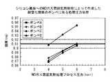
図3は、製造ロットの異なる4本のNOガスボンベA〜Dを用い、シリコン基板の表面に、NOガスを処理ガスとして用いた酸窒化処理により形成したシリコン酸窒化膜の処理圧力と膜厚との関係を示す特性図である。
ここでは、急速ランプ加熱処理装置を用い、処理温度950℃、処理時間20秒間の一定条件で、処理圧力を変えて酸窒化処理を行った。その結果、各々のNOガスボンベについて、同一処理圧力で得られる酸窒化膜厚に有意差が確認され、処理圧力に依存した膜厚変化に同一傾向が確認された。In a recent semiconductor manufacturing apparatus, the process pressure control has a structure that can sufficiently withstand a setting of less than 1.3 × 10² Pa (1 torr) by optimizing a gas supply system, an exhaust valve, and a control controller. .
FIG. 3 shows the processing pressure and film thickness of a silicon oxynitride film formed by oxynitriding treatment using NO gas as a processing gas on the surface of a silicon substrate using four NO gas cylinders A to D having different production lots. It is a characteristic view which shows the relationship.
Here, a rapid lamp heat treatment apparatus was used, and the oxynitriding treatment was performed by changing the treatment pressure under constant conditions of a treatment temperature of 950 ° C. and a treatment time of 20 seconds. As a result, for each NO gas cylinder, a significant difference was confirmed in the oxynitride film thickness obtained at the same processing pressure, and the same tendency was confirmed in the film thickness change depending on the processing pressure.
即ち、各NOガスボンベに応じて処理圧力を微調整することにより、安定して所望の膜厚のシリコン酸窒化膜が得られることを見出した。例えば、中心値0.91nmでバラツキ±0.01nmに制御したいとすれば、NOガスボンベAでは8.3×10²Pa(6.2torr)に、NOガスボンベCでは5.6×10²Pa(4.2torr)に設定すれば良い。
なお、上記の例では、酸窒化処理の条件を処理温度950℃、処理時間20秒間としたが、例えば1000℃や900℃等の異なる処理温度、異なる処理時間でも、処理圧力による変化の割合に違いはあるが、同様に所望する膜厚を得るための処理圧力の設定が可能である。That is, it has been found that a silicon oxynitride film having a desired film thickness can be stably obtained by finely adjusting the processing pressure in accordance with each NO gas cylinder. For example, if it is desired to control the variation to ± 0.01 nm with a center value of 0.91 nm, the NO gas cylinder A is 8.3 × 10² Pa (6.2 torr), and the NO gas cylinder C is 5.6 × 10² Pa ( 4.2 torr).
In the above example, the conditions for the oxynitriding process are set to a processing temperature of 950 ° C. and a processing time of 20 seconds. However, even at different processing temperatures such as 1000 ° C. and 900 ° C. and different processing times, Although there is a difference, a processing pressure for obtaining a desired film thickness can be similarly set.
図4は、シリコン基板の表面に、NOガスを処理ガスとして用いた酸窒化処理により形成したシリコン酸窒化膜の膜厚と各不純物濃度との関係を示す特性図である。
酸窒化処理は、処理温度950℃、処理圧力6.7×10²Pa(5torr)の条件で行った。ここでは、NO2,N2Oの各不純物濃度と、NO2+N2Oの不純物濃度とに分けてプロットした。膜厚感度は主にN2Oの不純物濃度に依存している。この場合、N2Oにおいて分解精製されるO2等によって酸化速度が増速すると考えられる。FIG. 4 is a characteristic diagram showing the relationship between the thickness of a silicon oxynitride film formed on the surface of a silicon substrate by oxynitriding using NO gas as a processing gas and the concentration of each impurity.
The oxynitriding treatment was performed under conditions of a treatment temperature of 950 ° C. and a treatment pressure of 6.7 × 10² Pa (5 torr). Here, each of the NO2 and N2 O impurity concentrations and the NO2 + N2 O impurity concentration are plotted separately. The film thickness sensitivity mainly depends on the impurity concentration of N2 O. In this case, it is considered that the oxidation rate is increased by O2 or the like decomposed and purified in N2 O.
一方、シリコン酸窒化膜を一定膜厚に形成するための不純物濃度と処理圧力との関係についても調べた。
図5は、シリコン基板の表面にNOガスを処理ガスとして用いた酸窒化処理を施した際の処理圧力と各不純物濃度との関係を示す特性図である。酸窒化処理は、処理温度950℃で膜厚0.91nmのシリコン酸窒化膜が得られるように行われた。このように、処理ガスの各不純物濃度は、処理圧力と明確な相関関係があることが判った。On the other hand, the relationship between the impurity concentration and the processing pressure for forming the silicon oxynitride film with a constant thickness was also examined.
FIG. 5 is a characteristic diagram showing the relationship between the processing pressure and the concentration of each impurity when an oxynitriding process using NO gas as the processing gas is performed on the surface of the silicon substrate. The oxynitriding treatment was performed so that a silicon oxynitride film having a thickness of 0.91 nm was obtained at a treatment temperature of 950 ° C. Thus, it was found that each impurity concentration of the processing gas has a clear correlation with the processing pressure.
以上、シリコン基板の表面に、NOガスを処理ガスとする酸窒化処理によりシリコン酸窒化膜を形成する場合について説明したが、シリコン基板の表面に形成されたシリコン酸化膜を酸窒化処理してシリコン酸窒化膜を形成する場合における、NOガスボンベを交換した際における膜厚への影響についても調べた。以下、この経緯について、図6,図7を用いて説明する。 As described above, the case where the silicon oxynitride film is formed on the surface of the silicon substrate by the oxynitriding process using NO gas as the processing gas has been described. However, the silicon oxide film formed on the surface of the silicon substrate is subjected to an oxynitriding process to form silicon. The influence on the film thickness when the NO gas cylinder was replaced in the case of forming the oxynitride film was also examined. Hereinafter, this process will be described with reference to FIGS.
図6は、10月8日〜11月5日に亘り、シリコン基板の表面にNOガスを処理ガスとして用いた酸窒化処理(処理A)により形成したシリコン酸窒化膜(図1と同結果)と、シリコン基板の表面に酸化処理(処理B)により形成したシリコン酸化膜と、このシリコン酸化膜をNOガスを処理ガスとして用いた酸窒化処理(処理C)により形成したシリコン酸窒化膜とについて、それぞれ膜厚を示す特性図である。ここで、処理Aは、処理温度950℃、処理圧力6.7×10²Pa(5torr)の条件、処理Bは、処理温度900℃、処理圧力6.7×10²Pa(5torr)の条件、処理Cは、処理温度950℃、処理圧力6.7×10²Pa(5torr)の条件でそれぞれ実行した。6 shows a silicon oxynitride film formed by oxynitriding treatment (treatment A) using NO gas as a processing gas on the surface of a silicon substrate from October 8 to November 5 (the same result as FIG. 1). And a silicon oxide film formed on the surface of the silicon substrate by an oxidation process (process B), and a silicon oxynitride film formed by an oxynitridation process (process C) using this silicon oxide film as a processing gas. FIG. 5 is a characteristic diagram showing a film thickness. Here, the treatment A is a treatment temperature of 950 ° C. and a treatment pressure of 6.7 × 10² Pa (5 torr), and the treatment B is a treatment temperature of 900 ° C. and a treatment pressure of 6.7 × 10² Pa (5 torr). The process C was performed under the conditions of a processing temperature of 950 ° C. and a processing pressure of 6.7 × 10² Pa (5 torr).
図1と同様に、破線で示す10月24日〜10月30日の間でNOガスボンベを交換しており、この間で処理Cでは処理Aと同等の膜厚の変化が確認される。図2の結果を図1と併せて考察すれば、シリコン酸化膜の酸窒化処理により形成されるシリコン酸窒化膜の膜厚も、処理ガスであるNOガス中に存在するNO2,N2Oの不純物含有量と強い相関関係があることが判る。As in FIG. 1, the NO gas cylinder is exchanged between October 24 and October 30 indicated by a broken line, and during this time, in process C, a change in film thickness equivalent to process A is confirmed. Considering the result of FIG. 2 together with FIG. 1, the film thickness of the silicon oxynitride film formed by the oxynitriding process of the silicon oxide film is also NO2 , N2 O present in the NO gas as the processing gas. It can be seen that there is a strong correlation with the impurity content.
同様に、例えば膜厚0.85nm程度のシリコン酸化膜に対して、プラズマ窒化を行い、続いて処理温度950℃、処理圧力6.7×10²Pa(5torr)の条件でNOガスを処理ガスとして用いた酸窒化処理を行った場合にも、処理A,Cに比べて程度は小さいが同様な変化が確認された。Similarly, for example, plasma nitridation is performed on a silicon oxide film having a thickness of about 0.85 nm, and subsequently, NO gas is treated with a processing gas at a processing temperature of 950 ° C. and a processing pressure of 6.7 × 10² Pa (5 torr). Even when the oxynitriding treatment used as was performed, a similar change was confirmed although the degree was small compared to the treatments A and C.
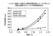
図7は、シリコン基板の表面に酸化処理によりシリコン酸化膜を形成し、このシリコン酸化膜をNOガスを処理ガスとして用いた酸窒化処理することにより形成したシリコン酸窒化膜について、酸窒化処理の処理圧力と膜厚との関係を示す特性図である。
酸化処理は、急速ランプ加熱処理により、処理温度900℃、処理圧力6.7×10²Pa(5torr)の条件で行い、膜厚0.85nmのシリコン酸化膜を形成した。酸窒化処理は、処理温度950℃、処理時間20秒間の条件で行った。このように、形成されたシリコン酸窒化膜の膜厚は、酸窒化処理の処理圧力と明確な相関関係があることが判った。FIG. 7 shows a silicon oxynitride film formed by forming a silicon oxide film on the surface of a silicon substrate by an oxidization process and subjecting the silicon oxide film to an oxynitride process using NO gas as a process gas. It is a characteristic view which shows the relationship between a process pressure and a film thickness.
The oxidation treatment was performed by rapid lamp heat treatment under the conditions of a treatment temperature of 900 ° C. and a treatment pressure of 6.7 × 10² Pa (5 torr) to form a silicon oxide film having a thickness of 0.85 nm. The oxynitriding treatment was performed under conditions of a treatment temperature of 950 ° C. and a treatment time of 20 seconds. Thus, it was found that the film thickness of the formed silicon oxynitride film has a clear correlation with the processing pressure of the oxynitriding process.
(2)酸窒化処理において、処理ガス中の不純物濃度と、形成されたシリコン酸窒化膜の窒素濃度との相関関係について
本発明者は、シリコン基板の表面に形成されたシリコン窒化膜を酸窒化処理してなるシリコン酸窒化膜について、その膜厚と共に、当該シリコン酸窒化膜の含有する窒素濃度について、酸窒化処理における処理圧力の依存性について調べた。(2) Correlation between impurity concentration in process gas and nitrogen concentration of formed silicon oxynitride film in oxynitridation treatment The present inventors have oxynitrided a silicon nitride film formed on the surface of a silicon substrate With respect to the silicon oxynitride film obtained by the treatment, the dependency of the treatment pressure in the oxynitriding treatment was examined on the nitrogen concentration contained in the silicon oxynitride film together with the film thickness.
図8は、シリコン基板の表面に酸化処理によりシリコン酸化膜を形成し、このシリコン酸化膜をNOガスを処理ガスとして用いた酸窒化処理することにより形成したシリコン酸窒化膜について、酸窒化処理の処理圧力と膜厚及び窒素濃度との関係を示す特性図である。シリコン酸窒化膜の窒素濃度は、SIMS分析により、シリコン酸窒化膜のシリコン基板との界面における窒素濃度として測定した。 FIG. 8 shows a silicon oxynitride film formed by forming a silicon oxide film on the surface of a silicon substrate by an oxidization process, and subjecting the silicon oxide film to an oxynitride process using NO gas as a process gas. It is a characteristic view which shows the relationship between a process pressure, a film thickness, and nitrogen concentration. The nitrogen concentration of the silicon oxynitride film was measured as the nitrogen concentration at the interface between the silicon oxynitride film and the silicon substrate by SIMS analysis.
図示のように、シリコン酸窒化膜の膜厚と酸窒化処理の処理圧力との関係と同様に、シリコン酸窒化膜の窒素濃度は処理圧力と明確な相関関係があることが判った。
なお、処理ガス中の不純物濃度とシリコン酸窒化膜の窒素濃度との間については、処理ガス中の不純物濃度とシリコン酸窒化膜の膜厚との関係と同様に明確な相関関係があるものと言える。このことは、処理ガス中の不純物濃度とシリコン酸窒化膜の膜厚とが図4のように明確な相関を有し、図8でシリコン酸窒化膜の窒素濃度の変化が膜厚の変化と同様な振る舞いを示すことからも裏付けされる。As shown in the figure, it was found that the nitrogen concentration of the silicon oxynitride film has a clear correlation with the processing pressure, as well as the relationship between the film thickness of the silicon oxynitride film and the processing pressure of the oxynitriding process.
Note that there is a clear correlation between the impurity concentration in the process gas and the nitrogen concentration in the silicon oxynitride film, as well as the relationship between the impurity concentration in the process gas and the film thickness of the silicon oxynitride film. I can say that. This is because the impurity concentration in the processing gas and the film thickness of the silicon oxynitride film have a clear correlation as shown in FIG. 4, and the change in the nitrogen concentration of the silicon oxynitride film in FIG. This is supported by the similar behavior.
以上、(1),(2)で説明したように、NOガスを処理ガスとして用いた酸窒化処理で形成されたシリコン酸窒化膜では、その膜厚及び含有する窒素濃度が、処理ガスの各不純物濃度と明確な相関を有するとともに、処理圧力とも明確な相関を有することが明らかとなった。 As described above in (1) and (2), in the silicon oxynitride film formed by the oxynitriding process using NO gas as the processing gas, the film thickness and the concentration of nitrogen contained in each of the processing gases are different. It became clear that there was a clear correlation with the impurity concentration and a clear correlation with the processing pressure.
この結果に基づき、本実施形態では、NOガス中のNO2,N2Oの各不純物濃度と得られるシリコン酸窒化膜の膜厚又は窒素濃度との相関関係(例えば図4)を予め計測して規定しておく。同様に、酸窒化処理における処理圧力と膜厚又は窒素濃度との相関関係(例えば図5(膜厚を0.91nmとする場合)、図4及び図5、図7、図8等)を予め計測し規定しておく。Based on this result, in this embodiment, the correlation (for example, FIG. 4) between the impurity concentration of NO2 and N2 O in the NO gas and the thickness or nitrogen concentration of the obtained silicon oxynitride film is measured in advance. To prescribe. Similarly, the correlation between the processing pressure in the oxynitriding process and the film thickness or nitrogen concentration (for example, FIG. 5 (when the film thickness is 0.91 nm), FIG. 4, FIG. 5, FIG. 7, FIG. 8, etc.) Measure and prescribe.
そして、実際に酸窒化処理に用いる処理ガス(NOガス)の不純物濃度を計測する。
続いて、上記の相関関係に基づき、膜厚又は窒素濃度が所定範囲内の値となるように、計測された不純物濃度に応じて、具体的には酸窒化処理における処理圧力を、膜厚又は窒素濃度が所定範囲内の値となるように設定する。そして、このように処理圧力を設定した状態で、酸窒化処理を実行する。Then, the impurity concentration of the processing gas (NO gas) actually used for the oxynitriding process is measured.
Subsequently, based on the above correlation, the processing pressure in the oxynitriding process is specifically set to the film thickness or the nitrogen concentration according to the measured impurity concentration so that the film thickness or the nitrogen concentration falls within a predetermined range. The nitrogen concentration is set to a value within a predetermined range. Then, the oxynitriding process is performed with the processing pressure set in this way.
この構成により、酸窒化処理を行うときに、NOガスが自己分解により当初と異なる不純物濃度となることを考慮し、NO2,N2Oの各不純物濃度をモニターして、処理圧力にフィードバックさせることで、安定した所望の膜厚又は所望の窒素濃度の酸窒化膜を形成することができる。With this configuration, when oxynitriding is performed, NO2 and N2 O impurity concentrations are monitored and fed back to the processing pressure in consideration of the fact that NO gas has an impurity concentration different from the original due to self-decomposition. Thus, an oxynitride film having a stable desired film thickness or a desired nitrogen concentration can be formed.
ここで、シリコン酸窒化膜の膜厚及び窒素濃度は、上述したように共に処理ガス中の不純物濃度及び処理圧力と明確な相関を有しており、従って膜厚と窒素濃度との間も明確な相関関係にある。そのため、上記のように処理圧力を調節し、処理時間や処理温度等の諸条件を適宜制御して膜厚及び窒素濃度の一方が所望値となるように酸窒化膜を形成すれば、当該酸窒化膜は、他方も所望値に調節された状態で形成されると考えられる。ここで例えば、膜厚及び窒素濃度の所望値を独立にそれぞれ設定し、不純物濃度の計測値から各々の所望値を達成する処理圧力を算出して、双方の値から最適な処理圧力を決定する(例えば処理圧力の平均値を採用する)ようにしても好適である。 Here, both the film thickness and the nitrogen concentration of the silicon oxynitride film have a clear correlation with the impurity concentration and the processing pressure in the processing gas as described above, and therefore the film thickness and the nitrogen concentration are also clear. There is a strong correlation. Therefore, if the oxynitride film is formed so that one of the film thickness and the nitrogen concentration becomes a desired value by adjusting the processing pressure as described above and appropriately controlling various conditions such as processing time and processing temperature, the acid The nitride film is considered to be formed in a state where the other is adjusted to a desired value. Here, for example, the desired values of the film thickness and the nitrogen concentration are set independently, the processing pressure for achieving each desired value is calculated from the measured value of the impurity concentration, and the optimum processing pressure is determined from both values. (For example, an average value of the processing pressure is adopted).
以上、処理ガスとして用いるNOガス中の不純物濃度に応じたプロセス制御に関して述べてきたが、近年、不純物濃度を更なる高純度、例えば99.99%に制御したNOガスの精製が可能となっている。このような高純度のNOガスを用いる場合、自己分解による不純物濃度の増加が処理ガスに与える影響が大きくなるが、これは言わば処理ガスの成分変化を敏感に把握することができることを示唆していると考えられる。本発明者はこの点に着目して、以下のような調査を行った。 The process control according to the impurity concentration in the NO gas used as the processing gas has been described above. In recent years, it has become possible to purify NO gas with the impurity concentration controlled to a further high purity, for example, 99.99%. Yes. When such high-purity NO gas is used, the increase in the impurity concentration due to self-decomposition has a greater effect on the processing gas, which suggests that the change in the component of the processing gas can be grasped sensitively. It is thought that there is. The present inventor conducted the following investigation paying attention to this point.
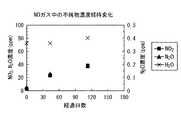
図9は、経過日数とNOガス中の各不純物濃度との関係を示す特性図である。
このNOガスは、99.99%に高純度に精製されたものであり、精製直後はN2O,NO2の各不純物濃度は10ppm以下に抑えられている。しかしながら、経過日数と共に不純物濃度は上昇し、120日後には各不純物濃度は40ppmを超えてしまった。この不純物濃度の上昇は、NOガスボンベへのNOガスの充填圧力や、保管環境によっても異なると考えられるが、高純度に精製しても、NOガス中の不純物濃度を長期間に亘って一定に保つことは不可能であることが判る。FIG. 9 is a characteristic diagram showing the relationship between the number of days elapsed and the concentration of each impurity in the NO gas.
This NO gas is refined to 99.99% with high purity, and immediately after purification, the impurity concentrations of N2 O and NO2 are suppressed to 10 ppm or less. However, the impurity concentration increased with the number of days elapsed, and after 120 days, each impurity concentration exceeded 40 ppm. This increase in impurity concentration is thought to vary depending on the filling pressure of NO gas into the NO gas cylinder and the storage environment, but the impurity concentration in the NO gas is kept constant over a long period of time even after purification to high purity. It turns out that it is impossible to keep.
図10は、図9で不純物濃度を調査したNOガスボンベを用いて、シリコン基板の表面に酸窒化処理により形成したシリコン酸窒化膜について、酸窒化処理の処理圧力と膜厚との関係を示す特性図である。
NOガスボンベの使用開始時、及び43日経過後までは、同一処理圧力で同様の膜厚が得られているが、113日経過後では、同一圧力で得られる膜厚が約0.01nm程度厚くなっている。同一膜厚を得るには、処理圧力を6.7×10Pa(0.5torr)程度低く設定する必要がある。FIG. 10 shows the relationship between the processing pressure and the film thickness of the oxynitriding process for the silicon oxynitride film formed on the surface of the silicon substrate by the oxynitriding process using the NO gas cylinder whose impurity concentration was investigated in FIG. FIG.
The same film thickness is obtained at the same processing pressure until the start of use of the NO gas cylinder and after 43 days, but after 113 days, the film thickness obtained at the same pressure becomes about 0.01 nm thick. Yes. In order to obtain the same film thickness, it is necessary to set the processing pressure as low as 6.7 × 10 Pa (0.5 torr).
図10について、図9の不純物濃度の分析結果と合わせて考察すると、各不純物濃度がそれぞれ30ppm程度となるまで、或いは図9でNO2,N2Oの各不純物濃度が共にほぼ30ppmであることから、各不純物濃度の合計が60ppm程度となるまでは、不純物濃度が膜厚変化に及ぼす影響は無視し得る範囲であり、膜厚変化に寄与せず、プロセス条件を変更する必要がないと考えられる。Considering FIG. 10 together with the analysis result of the impurity concentration in FIG. 9, each impurity concentration is about 30 ppm, or in FIG. 9, the impurity concentrations of NO2 and N2 O are both about 30 ppm. Therefore, until the total concentration of each impurity reaches about 60 ppm, the influence of the impurity concentration on the change in film thickness is negligible, it does not contribute to the change in film thickness, and there is no need to change the process conditions. It is done.
この結果に基づき、本実施形態では、高純度、例えば99.99%程度に精製されたNOガスを処理ガスとして用いる場合、先ず、実際に酸窒化処理に用いる処理ガス(NOガス)のN2O,NO2の各不純物濃度を計測する。その結果、計測された各不純物濃度が所定値、例えばそれぞれ30ppm以下、或いは各不純物濃度の合計が所定値、例えば60ppm以下であれば、敢えて上述のように処理圧力の調節等のプロセス条件を変更することなく、そのまま酸窒化処理を行う。そして、処理ガスの不純物濃度を測定した結果、その値が所定範囲を逸脱する場合には、上記した各相関関係に基づいて処理圧力を調節して酸窒化処理を行えば良い。Based on this result, in this embodiment, when NO gas purified to a high purity, for example, about 99.99%, is used as the processing gas, first, N2 of the processing gas (NO gas) actually used for the oxynitriding process is used. The impurity concentrations of O and NO2 are measured. As a result, if each measured impurity concentration is a predetermined value, for example, 30 ppm or less, or the total of each impurity concentration is a predetermined value, for example, 60 ppm or less, the process conditions such as adjustment of the processing pressure are changed as described above. The oxynitridation process is performed as it is. Then, as a result of measuring the impurity concentration of the processing gas, if the value deviates from the predetermined range, the oxynitriding process may be performed by adjusting the processing pressure based on the above-described correlations.
この構成により、酸窒化処理を行うときに、処理ガスが自己分解により当初と異なる不純物濃度となる場合を考慮しても、当該処理ガスの不純物濃度を測定し、各不純物濃度がそれぞれ30ppm以下、或いはその合計が60ppm以下であることを確認するだけで、処理圧力の設定の何等の調節も行うことなく、膜厚又は窒素濃度が所定範囲内とされた所期の酸窒化膜を容易且つ確実に形成することができる。 With this configuration, even when considering the case where the processing gas has an impurity concentration different from the original due to self-decomposition when performing the oxynitriding treatment, the impurity concentration of the processing gas is measured, and each impurity concentration is 30 ppm or less, Alternatively, by simply confirming that the total is 60 ppm or less, the desired oxynitride film whose film thickness or nitrogen concentration is within a predetermined range can be easily and reliably obtained without any adjustment of the processing pressure setting. Can be formed.
更に本実施形態では、上記とは別個の構成として、各不純物濃度がそれぞれ10ppm以下に調節されたNOガス、或いは図9で各不純物濃度(NxOy組成(0<x≦2,0<y≦2,x≠y)の不純物に限る。ここではN2O,NO2)がほぼ同値であることから、各不純物濃度の合計が20ppm以下に調節されたNOガスを処理ガスとして用いる。この場合、図9及び図10の結果から、当該NOガスの経過日数がその精製直後から例えば43日以内であれば、その各不純物濃度(N2O,NO2の各濃度)がそれぞれ30ppm以下、或いは各不純物濃度の合計が60ppm以下であると見なせることから、当該不純物濃度を計測することなく、そのまま酸窒化処理を行うことができる。Further, in the present embodiment, as a configuration different from the above, NO gas in which each impurity concentration is adjusted to 10 ppm or less, or each impurity concentration (Nx Oy composition (0 <x ≦ 2, 0 < This is limited to impurities of y ≦ 2, x ≠ y), where N2 O, NO2 ) are almost the same value, and therefore, NO gas whose total impurity concentration is adjusted to 20 ppm or less is used as the processing gas. In this case, from the results of FIG. 9 and FIG. 10, if the elapsed days of the NO gas are within 43 days immediately after the purification, the respective impurity concentrations (N2 O and NO2 concentrations) are 30 ppm or less, respectively. Alternatively, since the total of the impurity concentrations can be regarded as 60 ppm or less, the oxynitriding treatment can be performed as it is without measuring the impurity concentration.
この構成により、酸窒化処理を行うときに、処理ガスが自己分解により当初と異なる不純物濃度となる場合を考慮しても、当初の各不純物濃度がそれぞれ10ppm以下、或いは各不純物濃度の合計が例えば20ppm以下であることが確認されていれば、当該処理ガスの経過日数を把握しておくだけで、不純物濃度の計測等の如き何等の作業も行うことなく、膜厚又は窒素濃度が所定範囲内とされた所期の酸窒化膜を容易且つ確実に形成することができる。 With this configuration, even when considering the case where the process gas has an impurity concentration different from the original due to self-decomposition when performing the oxynitriding treatment, the initial impurity concentration is 10 ppm or less, or the total of the impurity concentrations is, for example, If it is confirmed that the concentration is 20 ppm or less, the film thickness or the nitrogen concentration is within the predetermined range without performing any operation such as measurement of the impurity concentration by just grasping the elapsed days of the processing gas. The desired oxynitride film can be easily and reliably formed.
(本実施形態による酸窒化処理の具体的構成)
以下、上述した経緯を踏まえ、本実施形態による酸窒化処理について説明する。
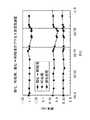
図11は、本実施形態による酸窒化処理装置の概略構成を示す模式図である。(Specific configuration of oxynitriding treatment according to this embodiment)
The oxynitriding process according to the present embodiment will be described below based on the above-described background.
FIG. 11 is a schematic diagram showing a schematic configuration of the oxynitriding apparatus according to the present embodiment.
図11において、1は被処理体10である例えばシリコン基板が載置固定される処理チャンバーである。2は、当該酸窒化処理装置の制御部であり、処理チャンバー1内の温度を制御する温度調節部2a、処理チャンバー1内に供給される処理ガス(NOガス)及び希釈ガスの各流量を制御する流量調節部2bとを有している。3は、処理チャンバー1内にガスを供給するガス供給部であり、処理ガスであるNOガスが封入されたNOガスボンベ3aと、希釈ガスであるN2ガスや不活性ガス(Ar,He等)が封入された希釈ガスボンベ3bとを有している。In FIG. 11,
4は、NOガスボンベ3aに封入されている処理ガス内の不純物であるNO2、N2Oの各不純物濃度を計測する濃度計測部であり、ガスクロマトグラフィー法や、FT−IR(フーリエ変換赤外分光)法等により濃度計測を行う。この濃度計測部4は、ガス供給部3のNOガスボンベ3aから処理チャンバー1への処理ガスの供給経路(に設けられている。)から分岐されて設けられている。4 is a concentration measuring unit for measuring the concentration of impurities of NO2 and N2 O, which are impurities in the processing gas sealed in the NO gas cylinder 3a, and includes gas chromatography and FT-IR (Fourier transform red). Concentration measurement is performed by an external spectroscopy method or the like. The
5は、濃度計測部4で計測されたNOガスボンベ3a内の処理ガスの各不純物濃度について、諸々の判定を行う濃度判定部である。この濃度判定部5は、計測された各不純物濃度が後述する記録部6に記録された諸データの測定範囲内にあるか否かを判定する第1の判定動作と、計測された各不純物濃度が所定のしきい値、例えば30ppm以下であるか否かを判定する第2の判定動作とを行う。例えば第2の判定動作において、各不純物濃度がしきい値であると判定された場合、処理圧力設定等の制御工程を行うことなく、酸窒化処理を開始することができる。
6は、予め規定された、処理ガス中の各不純物濃度と、酸窒化処理により形成されるシリコン酸窒化膜の膜厚又はシリコン酸窒化膜の窒素濃度と、酸窒化処理の処理圧力(酸窒化処理時における処理チャンバー1内の設定圧力)との相関関係の諸データをコンピュータ読み取り可能に記録する記録部である。記録部6には、例えば図4等に示すNOガス中のNO2,N2Oの各不純物濃度と得られるシリコン酸窒化膜の膜厚又は窒素濃度との相関関係や、例えば図5(膜厚を0.91nmとする場合)、図4及び図5、図7、図8等に示す酸窒化処理における処理圧力と膜厚又は窒素濃度との相関関係等のデータが記録されている。なお、記録部6と共に、或いはその代わりに、例えばNOガスボンベの管理状態(保管温度や保管時間等)と共に上記の諸データを管理するようにデータベースを設けるようにしても好適である。6 shows a predetermined concentration of each impurity in the processing gas, a film thickness of the silicon oxynitride film formed by the oxynitriding process or a nitrogen concentration of the silicon oxynitride film, and a processing pressure of the oxynitriding process (oxynitriding) It is a recording unit that records various data of correlation with a set pressure in the
7は、当該酸窒化処理における適正な処理圧力を算出する圧力算出部である。即ち、圧力算出部7は、濃度判定部5で各不純物濃度がしきい値(例えば30ppm)を越えていると判定された場合において、記録部6に記録されている上記の諸データを用い、濃度計測部4で計測された各不純物濃度に応じて、酸窒化処理により生成される酸窒化膜の膜厚又は酸窒化膜の窒素濃度が所定範囲内の値となるように、当該酸窒化処理における処理圧力を決定する。この圧力算出部7は、最適な処理圧力を算出する際に、例えば上記したNOガスボンベの管理状態を勘案して、管理温度や管理時間等に基づいて諸データを適宜補正し、所望の膜厚又は窒素濃度を得るために、より正確な処理圧力を設定するようにしても好適である。
制御部2は、圧力算出部7で決定された最適な処理圧力を実現すべく、排気系に設けられたポンプに繋がる圧力調整バルブの開閉度を調整することで、チャンバー1内の圧力を調整する。温度調節部2aにより処理チャンバー1内の温度を、流量調節部2bにより処理チャンバー1内に供給する処理ガス及び希釈ガスの各流量をそれぞれ調節する。 The
以下、上記した構成の酸窒化処理装置を用いた酸窒化処理方法について説明する。
図12は、本実施形態による酸窒化処理方法をステップ順に示すフロー図であり、(a)には当該酸窒化処理の前提となる諸データの作成プロセスを、(b)には作成された諸データを用いた当該酸窒化処理のプロセスをそれぞれ示す。
る。Hereinafter, an oxynitriding method using the oxynitriding apparatus configured as described above will be described.
FIG. 12 is a flowchart showing the oxynitriding method according to the present embodiment in the order of steps. FIG. 12A shows a process for creating various data as a premise of the oxynitriding process, and FIG. The process of the oxynitriding process using the data is shown.
The
先ず、図12(a)に示すように、当該酸窒化処理の前提となる、処理ガス中の各不純物濃度と、酸窒化処理により形成されるシリコン酸窒化膜の膜厚又はシリコン酸窒化膜の窒素濃度と、酸窒化処理の処理圧力との相関関係の諸データを作成する(ステップS1)。
例えば、図4等に示すNOガス中のNO2,N2Oの各不純物濃度と得られるシリコン酸窒化膜の膜厚又は窒素濃度との相関関係や、例えば図3(膜厚を0.91nmとする場合)、図4及び図5、図7、図8等に示す酸窒化処理における処理圧力と膜厚又は窒素濃度との相関関係等のデータが作成される。
そして、作成された諸データを記録部6(又は所定のデータベース等)に記録する(ステップS2)。First, as shown in FIG. 12A, each impurity concentration in the processing gas, which is a premise of the oxynitriding process, and the thickness of the silicon oxynitride film formed by the oxynitriding process or the silicon oxynitride film Various data on the correlation between the nitrogen concentration and the treatment pressure of the oxynitriding treatment are created (step S1).
For example, the correlation between the impurity concentration of NO2 and N2 O in the NO gas shown in FIG. 4 and the film thickness or nitrogen concentration of the obtained silicon oxynitride film, for example, FIG. In this case, data such as the correlation between the processing pressure and the film thickness or the nitrogen concentration in the oxynitriding process shown in FIGS. 4, 5, 7, and 8 is created.
Then, the created various data is recorded in the recording unit 6 (or a predetermined database or the like) (step S2).
上記したステップS1,S2は、個々の酸窒化処理の前提となる工程であり、実際の酸窒化処理を行う際に、当該酸窒化処理に伴って常に行うことを要するものではない。後述する場合(不純物濃度が諸データの作成範囲を逸脱する場合)を除き、ステップS1,S2を伴うことなく当該酸窒化処理を実行することができる。 Steps S1 and S2 described above are processes that are preconditions for individual oxynitriding treatments, and it is not always necessary to perform the actual oxynitriding treatment with the oxynitriding treatment. The oxynitriding process can be executed without steps S1 and S2, except when described later (when the impurity concentration deviates from the data creation range).
続いて、図12(b)に示すように、当該酸窒化処理を実行する。
先ず、当該酸窒化処理における、酸窒化膜、例えばシリコン酸窒化膜の膜厚又は窒素濃度、或いは膜厚及び窒素濃度の双方について、所望する所定値(所望する一定値と見なせる管理値の範囲:例えば、膜厚では0.91nm±0.01nm、窒素濃度では4.15at%±0.1at%を設定する(ステップS11)。Subsequently, as shown in FIG. 12B, the oxynitriding process is performed.
First, in the oxynitriding process, a film thickness or nitrogen concentration of an oxynitride film, for example, a silicon oxynitride film, or a desired predetermined value (range of management values that can be regarded as a desired constant value: For example, the film thickness is set to 0.91 nm ± 0.01 nm, and the nitrogen concentration is set to 4.15 at% ± 0.1 at% (step S11).
続いて、濃度計測部4は、NOガスボンベ3a内の処理ガスの不純物であるNO2、N2Oの各不純物濃度を、ガスクロマトグラフィー法や、FT−IR(フーリエ変換赤外分光)法等により計測する(ステップS12)。Subsequently, the
続いて、濃度判定部5は、計測された各不純物濃度が後述する記録部6に記録された諸データの測定範囲内にあるか否かを判定する第1の判定動作を行う(ステップS13)。
ステップS13において、計測された各不純物濃度が記録部5に記録された諸データの測定範囲内にあると判定された場合、ステップS14以降へ進む。
一方、ステップS13において、計測された各不純物濃度が記録部6に記録された諸データの測定範囲を逸脱すると判定された場合、当該不純物濃度を含むように諸データを再作成する必要があるため、再びステップS1を実行する。Subsequently, the
In step S13, when it is determined that each measured impurity concentration is within the measurement range of various data recorded in the
On the other hand, if it is determined in step S13 that each measured impurity concentration deviates from the measurement range of the various data recorded in the
なお、ステップS1により作成された諸データが、想定される不純物濃度の計測値を十分に含むものであると考えられる場合には、このステップS13を省略することも可能である。 Note that if it is considered that the various data created in step S1 sufficiently include the measured values of the assumed impurity concentration, step S13 can be omitted.
続いて、濃度判定部5は、濃度計測部4で計測されたNOガスボンベ3a内の処理ガスの各不純物濃度が所定のしきい値、ここでは各不純物濃度の合計が60ppm以下であるか否かを判定する第2の判定動作を行う(ステップS14)。
ステップS14において、各不純物濃度の合計が60ppm以下であると判定された場合には、処理圧力設定等の制御ステップは不要である。即ち、当該処理ガスを用いて酸窒化処理を実行すれば、管理値の範囲内の膜厚及び窒素濃度に酸窒化膜が形成されると見込むことができる。従ってこの場合、制御部2は、当該酸窒化処理を開始する(ステップS17)。
一方、ステップS14において、各不純物のうち、各不純物濃度の合計が60ppmより大値のものがあると判定された場合には、ステップS15以降へ進む。Subsequently, the
In step S14, when it is determined that the total concentration of impurities is 60 ppm or less, a control step such as processing pressure setting is not necessary. That is, if the oxynitriding process is performed using the processing gas, it can be expected that an oxynitride film is formed with a film thickness and a nitrogen concentration within the control value range. Therefore, in this case, the
On the other hand, if it is determined in step S14 that there are impurities whose total concentration is greater than 60 ppm, the process proceeds to step S15 and subsequent steps.
続いて、圧力算出部7は、記録部6に記録されている上記の諸データを用い、ステップS1で計測された各不純物濃度に応じて、酸窒化処理により生成される酸窒化膜の膜厚又は酸窒化膜の窒素濃度が管理値の範囲内の値となるように、当該酸窒化処理における処理圧力を算出する(ステップS15)。Subsequently, the
続いて、制御部2は、温度調節部2a及び流量調節部2bを調節制御し、圧力算出部7で処理チャンバー内を圧力算出部7で算出された処理圧力に設定する(ステップS16)。
しかる後、制御部2は、当該酸窒化処理を開始する(ステップS17)。Subsequently, the
Thereafter, the
なお、NOガスボンベ3aとして、例えば、封入されているNOガスの不純物であるN2O,NO2,H2O等のうち、形成される酸窒化膜の膜厚及び窒素濃度の変動に寄与するNxOy組成(0<x≦2,0<y≦2,x≠y)の不純物、ここではN2O,NO2の濃度の合計が所定値、例えば20ppm以下に調節されてなるものを使用しても良い。この場合、所定の管理状態、例えば図9及び図10のデータを作成した際と同様の管理状態(NOガスボンベの保管温度やNOガスボンベへのNOガスの封入圧等)であるならば、当該NOガスの経過日数がその精製直後から例えば43日以内であれば、各不純物濃度の合計が60ppm以下であると見なせることから、当該不純物濃度を計測することなく、そのまま酸窒化処理(ステップS17)を行うことができる。ここで、当該NOガスの経過日数がその精製直後から例えば44日以後であれば、上記と同様にステップS11〜S17を行えば良い。As the NO gas cylinder 3a, for example, among the N2 O, NO2 , H2 O and the like that are the impurities of the enclosed NO gas, it contributes to fluctuations in the thickness of the formed oxynitride film and the nitrogen concentration. Impurities of Nx Oy composition (0 <x ≦ 2, 0 <y ≦ 2, x ≠ y), where the total concentration of N2 O and NO2 is adjusted to a predetermined value, for example, 20 ppm or less May be used. In this case, if it is a predetermined management state, for example, a management state similar to that at the time of creating the data of FIG. 9 and FIG. 10 (NO gas storage temperature, NO gas sealing pressure in the NO gas cylinder, etc.) If the elapsed time of the gas is within 43 days immediately after purification, for example, the total concentration of impurities can be considered to be 60 ppm or less. Therefore, the oxynitridation treatment (step S17) is directly performed without measuring the impurity concentration. It can be carried out. Here, if the elapsed days of the NO gas are, for example, 44 days after immediately after the purification, steps S11 to S17 may be performed in the same manner as described above.
以下、上記した酸窒化処理を、半導体装置、例えばMOSトランジスタの製造方法に適用した場合を例示する。
なお本発明は、MOSトランジスタ以外の半導体装置、例えばnMOSトランジスタ及びpMOSトランジスタを有するCMOSトランジスタや、各種の不揮発性半導体メモリ、キャパシタ構造を有する半導体メモリ等、種々の半導体装置に適用することができる。
図13は、本実施形態によるMOSトランジスタの製造方法を工程順に示す概略断面図である。Hereinafter, a case where the above-described oxynitriding process is applied to a method for manufacturing a semiconductor device, for example, a MOS transistor will be exemplified.
The present invention can be applied to various semiconductor devices such as semiconductor devices other than MOS transistors, such as CMOS transistors having nMOS transistors and pMOS transistors, various nonvolatile semiconductor memories, and semiconductor memories having a capacitor structure.
FIG. 13 is a schematic cross-sectional view showing the method of manufacturing the MOS transistor according to the present embodiment in the order of steps.
先ず、図13(a)に示すように、素子分離構造12を形成する。
詳細には、シリコン基板11の表層に例えばSTI(Shallow Trench Isolation)法により素子分離構造12を形成する。この素子分離構造12により、シリコン基板11で素子活性領域が確定される。First, as shown in FIG. 13A, the
Specifically, the
続いて、図13(b)に示すように、素子分離構造12には厚いシリコン酸化膜13を、素子活性領域にはゲート絶縁膜14をそれぞれ形成する。
詳細には、先ず、シリコン基板11の全面を例えば800℃でパイロジェニック酸化し、厚いシリコン酸化膜13を形成する。このシリコン酸化膜13のうち、素子活性領域上に形成された部分のみを例えばウェットエッチングにより除去する。これにより、素子分離構造12上のみに、例えば膜厚7nm程度のシリコン酸化膜13が残存する。Subsequently, as shown in FIG. 13B, a thick
Specifically, first, the entire surface of the
次に、表面が露出する素子活性領域を含むシリコン基板11の全面に、酸素雰囲気中で例えば900℃の酸化処理を行う。これにより、素子活性領域に例えば膜厚0.85nm程度のシリコン酸化膜(不図示)が形成される。なお、この酸化処理は、素子分離構造12上のシリコン酸化膜13にも施される。 Next, the entire surface of the
次に、上述した酸窒化処理装置を用い、上述した酸窒化処理方法により膜厚又は窒素濃度(或いは双方)を制御すべく処理ガスであるNOガスの不純物濃度を調節し、素子活性領域上のシリコン酸化膜に例えば950℃の酸窒化処理を施す。これにより、素子活性領域上のシリコン酸化膜が酸窒化され、例えば膜厚1.1nm程度のシリコン酸窒化膜であるゲート絶縁膜14が形成される。なお、この酸窒化処理は、素子分離構造12上のシリコン酸化膜13にも施される。 Next, using the above-described oxynitriding apparatus, the impurity concentration of NO gas, which is a processing gas, is adjusted to control the film thickness or nitrogen concentration (or both) by the above-described oxynitriding method. The silicon oxide film is subjected to an oxynitriding process at 950 ° C., for example. Thereby, the silicon oxide film on the element active region is oxynitrided, and the
続いて、図13(c)に示すように、ゲート電極15を形成する。
詳細には、ゲート絶縁膜14上に例えばCVD法により膜厚100nm程度の多結晶シリコン膜を堆積する。そして、多結晶シリコン膜及びゲート絶縁膜14をリソグラフィー及びドライエッチングにより電極形状に加工することにより、素子活性領域においてゲート絶縁膜14上にゲート電極15を形成する。Subsequently, as shown in FIG. 13C, a
Specifically, a polycrystalline silicon film having a thickness of about 100 nm is deposited on the
続いて、図13(d)に示すように、LDD領域16、サイドウォール絶縁膜17、及びソース/ドレイン領域18を順次形成する。
詳細には、先ず、ゲート電極15をマスクとして、素子活性領域に不純物(n型MOSトランジスタであればn型不純物(砒素(As)やリン(P)等)、p型MOSトランジスタであればp型不純物(ホウ素(B)等))をイオン注入し、ゲート電極15の両側における素子活性領域の表層に、いわゆるLDD領域16を形成する。Subsequently, as shown in FIG. 13D, an
Specifically, first, using the
次に、全面に例えばシリコン酸化膜を例えばCVD法により堆積し、このシリコン酸化膜をいわゆるエッチバックすることにより、素子活性領域におけるゲート電極15の側面のみにシリコン酸化膜を残して、サイドウォール絶縁膜17を形成する。 Next, for example, a silicon oxide film is deposited on the entire surface by, for example, a CVD method, and this silicon oxide film is so-called etched back, so that the silicon oxide film is left only on the side surface of the
次に、ゲート電極15及びサイドウォール絶縁膜17をマスクとして、素子活性領域に不純物(n型MOSトランジスタであればn型不純物(砒素(As)やリン(P)等)、p型MOSトランジスタであればp型不純物(ホウ素(B)等))をLDD領域16よりも不純物濃度が高くなる条件でイオン注入し、LDD領域16と重畳されるソース/ドレイン領域18を形成する。
このとき、半導体素子として、シリコン基板11上でゲート絶縁膜14を介して形成されたゲート電極15と、その両側に形成された一対のLDD領域16及びソース/ドレイン領域17とを有するトランジスタ構造20が完成する。Next, using the
At this time, as a semiconductor element, a
しかる後、トランジスタ構造20を覆う層間絶縁膜、及び種々の配線等の形成を経て、本実施形態のMOSトランジスタを完成させる。 Thereafter, an interlayer insulating film covering the
ここで、本発明の酸窒化処理を、当該NOガスの経過日数がその精製直後から所定日数経過した場合について、逐次処理圧力を調節してそれぞれゲート絶縁膜を形成した際の、各ゲート絶縁膜の膜厚及び界面窒素濃度(シリコン基板との界面)を調べた。その結果を図14に示す。
ここでは、NOガスの精製直後、43日経過時、113日経過時について、順に処理圧力を、調節なし、1.13×10³Pa(8.5torr)、1.07×10³Pa(8.0torr)として、酸窒化処理を行った。その結果、図示のように、これら全ての場合でゲート絶縁膜の膜厚及び界面窒素濃度が等しい値を示した。これは、本発明の酸窒化処理により膜厚及び界面窒素濃度を一定に保つことができ、極めて安定した所望のゲート絶縁膜が得られることを意味する。Here, in the oxynitriding treatment of the present invention, each gate insulating film when the gate insulating film is formed by adjusting the sequential processing pressure in the case where the predetermined number of days has passed since the purification of the NO gas immediately after the purification. The film thickness and interfacial nitrogen concentration (interface with the silicon substrate) were examined. The result is shown in FIG.
Here, immediately after the purification of NO gas, after 43 days, when 113 days have elapsed, the processing pressure is adjusted in order, 1.13 × 10³ Pa (8.5 torr), 1.07 × 10³ Pa (8 0.0 torr) was subjected to oxynitriding. As a result, as shown in the figure, the film thickness of the gate insulating film and the interface nitrogen concentration were equal in all of these cases. This means that the film thickness and interface nitrogen concentration can be kept constant by the oxynitriding treatment of the present invention, and a very stable desired gate insulating film can be obtained.
次に、図8で示したシリコン酸窒化膜をゲート絶縁膜としてMOSトランジスタを作製し、ゲートリーク電流密度を調べた。その結果を図15に示す。
図示のように、例えば0.01nm程度の膜厚差が5A/cm2の大きな感度を有することが確認された。従って、例えば図10に示すように、高純度に精製したNOガスを処理ガスに用いたとしても、NOガス中の不純物濃度に使用制限を設定せず、又はNOガス中の不純物によるプロセス条件補正を行うことのない従来の技術では、5A/cm2以上のリーク電流密度の変化をもたらしてしまう。Next, a MOS transistor was fabricated using the silicon oxynitride film shown in FIG. 8 as a gate insulating film, and the gate leakage current density was examined. The result is shown in FIG.
As shown in the figure, it was confirmed that a film thickness difference of, for example, about 0.01 nm has a large sensitivity of 5 A / cm2 . Therefore, for example, as shown in FIG. 10, even if high-purity NO gas is used as the processing gas, no limitation is set on the impurity concentration in the NO gas, or the process condition is corrected by the impurities in the NO gas. The conventional technique that does not perform the change causes a change in the leakage current density of 5 A / cm2 or more.
これに対して、図14の結果におけるNOガスの精製直後、43日経過時、113日経過時の各々について、ゲートリーク電流密度を調べた。その結果を図16に示す。
図示のように、これら全ての場合でゲート絶縁膜のゲートリーク電流密度が等しい値を示した。これは、本発明の酸窒化処理により、膜厚及び界面窒素濃度に加えてゲートリーク電流密度を一定に保つことができ、極めて安定した信頼性の高い所望のゲート絶縁膜が得られることを意味する。On the other hand, the gate leakage current density was examined for each of 43 days and 113 days immediately after purification of NO gas in the results of FIG. The result is shown in FIG.
As shown in the figure, the gate leakage current density of the gate insulating film showed the same value in all these cases. This means that the oxynitridation treatment of the present invention can keep the gate leakage current density constant in addition to the film thickness and interface nitrogen concentration, and can provide a highly stable and highly reliable desired gate insulating film. To do.
以上説明したように、本実施形態によれば、NOガスを処理ガスとして用いた酸窒化処理を行うに際して、当該酸窒化処理により所望の膜厚及び窒素濃度のシリコン酸窒化膜を得ることが可能となる。また、当該酸窒化処理を例えばMOSトランジスタの製造に適用することにより、高集積化及び微細化の要請に応える信頼性の高いMOSトランジスタが実現する。 As described above, according to the present embodiment, when an oxynitriding process using NO gas as a processing gas is performed, a silicon oxynitride film having a desired film thickness and nitrogen concentration can be obtained by the oxynitriding process. It becomes. In addition, by applying the oxynitriding process to, for example, the manufacture of a MOS transistor, a highly reliable MOS transistor that meets the demand for high integration and miniaturization can be realized.
なお、本実施形態では、MOSトランジスタにおけるゲート絶縁膜の成膜に、本発明の酸窒化処理を適用する場合について例示したが、本発明はこれに限定されるものではない。例えば、上記の例では、先ずシリコン酸化膜を形成した後、これを酸窒化してシリコン酸窒化膜を形成する場合について説明したが、シリコン基板の素子活性領域に、本発明の酸窒化処理により直接的にシリコン酸窒化膜を形成する場合にも適用可能である。また、先ずシリコン酸化膜を形成し、本発明の酸窒化処理によりこれを酸窒化してシリコン酸窒化膜を形成した後、プラズマ窒化法によるシリコン窒化膜を形成してゲート絶縁膜としたり、或いはHf,Zr,Al等のいわゆるHigh-K材料と呼ばれる高誘電率材料の薄膜を堆積し、ゲート絶縁膜を形成しても好適である。 In the present embodiment, the case where the oxynitriding treatment of the present invention is applied to the formation of the gate insulating film in the MOS transistor is exemplified, but the present invention is not limited to this. For example, in the above example, a case where a silicon oxide film is first formed and then oxynitrided to form a silicon oxynitride film has been described. However, the active region of the silicon substrate is subjected to the oxynitriding treatment of the present invention. The present invention can also be applied when directly forming a silicon oxynitride film. Alternatively, a silicon oxide film is first formed and then oxynitrided by the oxynitriding treatment of the present invention to form a silicon oxynitride film, and then a silicon nitride film is formed by plasma nitriding to form a gate insulating film, or It is also preferable to form a gate insulating film by depositing a thin film of a high dielectric constant material called a so-called High-K material such as Hf, Zr, or Al.
上述した本実施形態による酸窒化処理方法の各ステップ(図12のステップS12〜S17等)は、コンピュータのRAMやROMなどに記憶されたプログラムが動作することによって実現できる。このプログラム及び当該プログラムを記録したコンピュータ読み取り可能な記憶媒体は本発明に含まれる。 Each step (steps S12 to S17 in FIG. 12 and the like) of the oxynitriding method according to the present embodiment described above can be realized by operating a program stored in a RAM or ROM of a computer. This program and a computer-readable storage medium storing the program are included in the present invention.
具体的に、前記プログラムは、例えばCD−ROMのような記録媒体に記録し、或いは各種伝送媒体を介し、コンピュータに提供される。前記プログラムを記録する記録媒体としては、CD−ROM以外に、フレキシブルディスク、ハードディスク、磁気テープ、光磁気ディスク、不揮発性メモリカード等を用いることができる。他方、前記プログラムの伝送媒体としては、プログラム情報を搬送波として伝搬させて供給するためのコンピュータネットワークシステムにおける通信媒体を用いることができる。ここで、コンピュータネットワークとは、LAN、インターネットの等のWAN、無線通信ネットワーク等であり、通信媒体とは、光ファイバ等の有線回線や無線回線等である。 Specifically, the program is recorded on a recording medium such as a CD-ROM or provided to a computer via various transmission media. As a recording medium for recording the program, besides a CD-ROM, a flexible disk, a hard disk, a magnetic tape, a magneto-optical disk, a nonvolatile memory card, or the like can be used. On the other hand, as the program transmission medium, a communication medium in a computer network system for propagating and supplying program information as a carrier wave can be used. Here, the computer network is a WAN such as a LAN or the Internet, a wireless communication network, or the like, and the communication medium is a wired line such as an optical fiber or a wireless line.
また、本発明に含まれるプログラムとしては、供給されたプログラムをコンピュータが実行することにより上述の実施形態の機能が実現されるようなもののみではない。例えば、そのプログラムがコンピュータにおいて稼働しているOS(オペレーティングシステム)或いは他のアプリケーションソフト等と共同して上述の実施形態の機能が実現される場合にも、かかるプログラムは本発明に含まれる。また、供給されたプログラムの処理の全て或いは一部がコンピュータの機能拡張ボードや機能拡張ユニットにより行われて上述の実施形態の機能が実現される場合にも、かかるプログラムは本発明に含まれる。 Further, the program included in the present invention is not limited to the one in which the functions of the above-described embodiments are realized by the computer executing the supplied program. For example, such a program is also included in the present invention when the function of the above-described embodiment is realized in cooperation with an OS (operating system) or other application software running on the computer. Further, when all or part of the processing of the supplied program is performed by the function expansion board or function expansion unit of the computer and the functions of the above-described embodiment are realized, the program is also included in the present invention.
1 処理チャンバー
2 制御部
2a 温度調節部
2b 流量調節部
3 ガス供給部
3a NOガスボンベ
3b 希釈ガスボンベ
4 濃度計測部
5 濃度判定部
6 記録部
7 圧力算出部
10 被処理体
11 シリコン基板
12 素子分離構造
13 シリコン酸化膜
14 ゲート絶縁膜
15 ゲート電極
16 LDD領域
17 サイドウォール絶縁膜
18 ソース/ドレイン領域
20 トランジスタ構造DESCRIPTION OF
Claims (7)
Translated fromJapanese前記処理ガス中に存在し、前記処理ガス中で自己分解により増加するNxOy組成(0<x≦2,0<y≦2,x≠y)の1種又は複数種の不純物の濃度を計測する第1の工程と、
前記酸窒化処理により生成される酸窒化膜の膜厚又は前記酸窒化膜の窒素濃度が所定範囲内の値となるように、前記第1の工程で計測された前記不純物の濃度に応じて前記酸窒化処理を行う第2の工程と
を含むことを特徴とする酸窒化処理方法。When performing oxynitridation using NO gas as a processing gas,
Concentration of one or more impurities of Nx Oy composition (0 <x ≦ 2, 0 <y ≦ 2, x ≠ y) present in the processing gas and increasing by self-decomposition in the processing gas A first step of measuring
The film thickness of the oxynitride film generated by the oxynitriding treatment or the nitrogen concentration of the oxynitride film is set to a value within a predetermined range according to the impurity concentration measured in the first step. And a second step of performing an oxynitriding process.
被処理体を収容する処理チャンバーと、
前記処理ガスに存在し、前記処理ガス中で自己分解により増加するNxOy組成(0<x≦2,0<y≦2,x≠y)の1種又は複数種の不純物の濃度を計測する濃度計測部と、
前記濃度計測部で計測された前記不純物の濃度に応じて、前記酸窒化処理により生成される酸窒化膜の膜厚又は前記酸窒化膜の窒素濃度が所定範囲内の値となるように、前記酸窒化処理における処理圧力を算出する圧力算出部と、
前記処理ガス中で自己分解により増加するNxOy組成(0<x≦2,0<y≦2,x≠y)の1種又は複数種の前記不純物の濃度と、前記酸窒化処理により形成される前記酸窒化膜の膜厚又は前記酸窒化膜の窒素濃度と、前記酸窒化処理時における前記処理チャンバ―内の圧力との相関関係の諸データを記録する記録部と
を含むことを特徴とする酸窒化処理装置。An oxynitriding apparatus that performs oxynitriding using NO gas as a processing gas,
A processing chamber for storing the object to be processed;
The concentration of one or more impurities of Nx Oy composition (0 <x ≦ 2, 0 <y ≦ 2, x ≠ y) present in the processing gas and increased by self-decomposition in the processing gas. A concentration measuring unit to measure,
In accordance with the concentration of the impurity measured by the concentration measuring unit, the thickness of the oxynitride film generated by the oxynitriding process or the nitrogen concentration of the oxynitride film is a value within a predetermined range. A pressure calculating unit for calculating a processing pressure in the oxynitriding process;
The concentration of one or more of the impurities ofNxOycomposition (0 <x ≦ 2, 0 <y ≦ 2, x ≠ y) thatincreases by self-decomposition in the processing gas, and theoxynitriding treatment A recording unit for recording various data of correlation between a film thickness of the formed oxynitride film or a nitrogen concentration of the oxynitride film and a pressure in the processing chamber during the oxynitriding process. A featured oxynitriding apparatus.
前記酸窒化膜に、NOガスを処理ガスとして用いた酸窒化処理を行うに際して、
前記処理ガス中に存在し、前記処理ガス中で自己分解により増加するNxOy組成(0<x≦2,0<y≦2,x≠y)の1種又は複数種の不純物の濃度を計測する第1の工程と、
前記酸窒化処理により生成される前記酸窒化膜の膜厚又は前記酸窒化膜の窒素濃度が所定範囲内の値となるように、前記第1の工程で計測された前記不純物の濃度に応じて前記酸窒化処理を行う第2の工程と
を含むことを特徴とする半導体装置の製造方法。A method of manufacturing a semiconductor device having an oxynitride film formed on a surface of a semiconductor substrate or above the semiconductor substrate,
When performing an oxynitriding process using NO gas as a processing gas on the oxynitride film,
Concentration of one or more impurities of Nx Oy composition (0 <x ≦ 2, 0 <y ≦ 2, x ≠ y) present in the processing gas and increasing by self-decomposition in the processing gas A first step of measuring
According to the impurity concentration measured in the first step so that the film thickness of the oxynitride film generated by the oxynitriding process or the nitrogen concentration of the oxynitride film is a value within a predetermined range. And a second step of performing the oxynitriding treatment.
Priority Applications (1)
| Application Number | Priority Date | Filing Date | Title |
|---|---|---|---|
| JP2007213924AJP5176428B2 (en) | 2007-08-20 | 2007-08-20 | Oxynitriding apparatus and method, and semiconductor device manufacturing method |
Applications Claiming Priority (1)
| Application Number | Priority Date | Filing Date | Title |
|---|---|---|---|
| JP2007213924AJP5176428B2 (en) | 2007-08-20 | 2007-08-20 | Oxynitriding apparatus and method, and semiconductor device manufacturing method |
Publications (2)
| Publication Number | Publication Date |
|---|---|
| JP2009049196A JP2009049196A (en) | 2009-03-05 |
| JP5176428B2true JP5176428B2 (en) | 2013-04-03 |
Family
ID=40501151
Family Applications (1)
| Application Number | Title | Priority Date | Filing Date |
|---|---|---|---|
| JP2007213924AExpired - Fee RelatedJP5176428B2 (en) | 2007-08-20 | 2007-08-20 | Oxynitriding apparatus and method, and semiconductor device manufacturing method |
Country Status (1)
| Country | Link |
|---|---|
| JP (1) | JP5176428B2 (en) |
Families Citing this family (1)
| Publication number | Priority date | Publication date | Assignee | Title |
|---|---|---|---|---|
| JP6435175B2 (en)* | 2014-12-02 | 2018-12-05 | 株式会社堀場エステック | Decomposition detection device, decomposition detection method, program for decomposition detection device, concentration measurement device, and concentration control device |
Family Cites Families (6)
| Publication number | Priority date | Publication date | Assignee | Title |
|---|---|---|---|---|
| US5591681A (en)* | 1994-06-03 | 1997-01-07 | Advanced Micro Devices, Inc. | Method for achieving a highly reliable oxide film |
| JP3335492B2 (en)* | 1994-12-28 | 2002-10-15 | 三菱電機株式会社 | Thin film deposition equipment |
| US5939763A (en)* | 1996-09-05 | 1999-08-17 | Advanced Micro Devices, Inc. | Ultrathin oxynitride structure and process for VLSI applications |
| JPH10223783A (en)* | 1997-02-10 | 1998-08-21 | Hitachi Ltd | Semiconductor device and manufacturing method thereof |
| JP2000091337A (en)* | 1998-09-09 | 2000-03-31 | Toshiba Microelectronics Corp | Semiconductor device and manufacturing method thereof |
| JP4820596B2 (en)* | 2005-07-21 | 2011-11-24 | 住友精化株式会社 | Nitric oxide purification method |
- 2007
- 2007-08-20JPJP2007213924Apatent/JP5176428B2/ennot_activeExpired - Fee Related
Also Published As
| Publication number | Publication date |
|---|---|
| JP2009049196A (en) | 2009-03-05 |
Similar Documents
| Publication | Publication Date | Title |
|---|---|---|
| JP5070702B2 (en) | Semiconductor device manufacturing method and manufacturing apparatus | |
| US7429540B2 (en) | Silicon oxynitride gate dielectric formation using multiple annealing steps | |
| EP0617461B1 (en) | Oxynitride dielectric process for IC manufacture | |
| US8748992B2 (en) | MOS transistors including SiON gate dielectric with enhanced nitrogen concentration at its sidewalls | |
| US20080090425A9 (en) | Two-step post nitridation annealing for lower EOT plasma nitrided gate dielectrics | |
| KR20050021311A (en) | Thin film formation method and semiconductor device manufacturing method | |
| US20070218624A1 (en) | Semiconductor device and method of manufacturing the same | |
| US20060281264A1 (en) | Semiconductor device and method for fabricating the same | |
| JP2004335756A (en) | Semiconductor device and its manufacturing method | |
| US20090258505A1 (en) | Semiconductor device manufacturing method | |
| US7192887B2 (en) | Semiconductor device with nitrogen in oxide film on semiconductor substrate and method of manufacturing the same | |
| US7247914B2 (en) | Semiconductor device and method for fabricating the same | |
| JP2002151684A (en) | Semiconductor device and manufacturing method thereof | |
| JP5176428B2 (en) | Oxynitriding apparatus and method, and semiconductor device manufacturing method | |
| CN101770986B (en) | Method and device for reducing gate leakage current and controlling starting voltage offset | |
| TWI280624B (en) | Method for manufacturing semiconductor device | |
| WO2005074037A1 (en) | Method for manufacturing semiconductor device | |
| JP5141321B2 (en) | Manufacturing method of semiconductor device | |
| JP4028538B2 (en) | Semiconductor device manufacturing method and manufacturing apparatus thereof | |
| JP3834564B2 (en) | Semiconductor device and manufacturing method thereof | |
| JP3826792B2 (en) | Manufacturing method of semiconductor device | |
| US20040251495A1 (en) | Semiconductor device and manufacturing method of the same | |
| JPWO2005004224A1 (en) | Semiconductor device and manufacturing method thereof | |
| JPH08191067A (en) | Semiconductor device and manufacturing method thereof | |
| US20080242114A1 (en) | Thermal anneal method for a high-k dielectric |
Legal Events
| Date | Code | Title | Description |
|---|---|---|---|
| A621 | Written request for application examination | Free format text:JAPANESE INTERMEDIATE CODE: A621 Effective date:20100506 | |
| A977 | Report on retrieval | Free format text:JAPANESE INTERMEDIATE CODE: A971007 Effective date:20100820 | |
| A131 | Notification of reasons for refusal | Free format text:JAPANESE INTERMEDIATE CODE: A131 Effective date:20120731 | |
| A521 | Request for written amendment filed | Free format text:JAPANESE INTERMEDIATE CODE: A523 Effective date:20120928 | |
| TRDD | Decision of grant or rejection written | ||
| A01 | Written decision to grant a patent or to grant a registration (utility model) | Free format text:JAPANESE INTERMEDIATE CODE: A01 Effective date:20121211 | |
| A61 | First payment of annual fees (during grant procedure) | Free format text:JAPANESE INTERMEDIATE CODE: A61 Effective date:20121224 | |
| R150 | Certificate of patent or registration of utility model | Ref document number:5176428 Country of ref document:JP Free format text:JAPANESE INTERMEDIATE CODE: R150 | |
| S531 | Written request for registration of change of domicile | Free format text:JAPANESE INTERMEDIATE CODE: R313531 | |
| R350 | Written notification of registration of transfer | Free format text:JAPANESE INTERMEDIATE CODE: R350 | |
| LAPS | Cancellation because of no payment of annual fees |