JP5168377B2 - Touch panel sensor and method for manufacturing touch panel sensor - Google Patents
Touch panel sensor and method for manufacturing touch panel sensorDownload PDFInfo
- Publication number
- JP5168377B2 JP5168377B2JP2011066390AJP2011066390AJP5168377B2JP 5168377 B2JP5168377 B2JP 5168377B2JP 2011066390 AJP2011066390 AJP 2011066390AJP 2011066390 AJP2011066390 AJP 2011066390AJP 5168377 B2JP5168377 B2JP 5168377B2
- Authority
- JP
- Japan
- Prior art keywords
- pattern
- photosensitive
- touch panel
- shield
- panel sensor
- Prior art date
- Legal status (The legal status is an assumption and is not a legal conclusion. Google has not performed a legal analysis and makes no representation as to the accuracy of the status listed.)
- Expired - Fee Related
Links
Images


Landscapes
- Position Input By Displaying (AREA)
Description
Translated fromJapanese本発明は、基板と、基板上に所定パターンで設けられ、透明導電材料からなる下側パターンと、下側パターン上に所定パターンで設けられ、金属材料からなる上側パターンと、を備えたタッチパネルセンサに関する。また本発明は、当該タッチパネルセンサの製造方法に関する。 The present invention relates to a touch panel sensor comprising a substrate, a lower pattern provided on the substrate in a predetermined pattern and made of a transparent conductive material, and an upper pattern provided on the lower pattern in a predetermined pattern and made of a metal material. About. The present invention also relates to a method for manufacturing the touch panel sensor.
従来、基板と、基板上に所定のパターンで設けられ、タッチを検出する透明導電パターンと、透明導電パターンに電気的に接続された取出導電パターンと、を有するタッチパネルセンサが知られている。透明導電パターンは、一般に、透明導電材料からなる透明導電層をパターニングすることにより形成される。また取出導電パターンは、一般に、透明導電層上に設けられ、金属材料からなる金属層をパターニングすることにより形成される。また透明導電パターンからの信号を外部に伝達させる際の電気抵抗を低減するため、一般に、取出導電パターンと基板との間には透明導電層が介在されている。 Conventionally, a touch panel sensor having a substrate, a transparent conductive pattern that is provided on the substrate in a predetermined pattern and detects a touch, and an extraction conductive pattern that is electrically connected to the transparent conductive pattern is known. The transparent conductive pattern is generally formed by patterning a transparent conductive layer made of a transparent conductive material. The extraction conductive pattern is generally provided on the transparent conductive layer, and is formed by patterning a metal layer made of a metal material. In order to reduce the electrical resistance when a signal from the transparent conductive pattern is transmitted to the outside, a transparent conductive layer is generally interposed between the extraction conductive pattern and the substrate.
タッチパネルセンサの各パターンを基板の法線方向に沿った階層で区画して考える場合、透明導電層をパターニングすることにより得られる透明導電パターンなどのパターンは、取出導電パターンよりも基板側(下側)に位置する下側パターンとなっている。また、金属層をパターニングすることにより得られる取出導電パターンなどのパターンは、透明導電パターンよりも基板から遠ざかる側(上側)に位置する上側パターンとなっている。 When considering each pattern of the touch panel sensor in a hierarchy along the normal direction of the substrate, the pattern such as the transparent conductive pattern obtained by patterning the transparent conductive layer is closer to the substrate side (lower side) than the extracted conductive pattern. ) Is located on the lower pattern. Further, a pattern such as an extraction conductive pattern obtained by patterning the metal layer is an upper pattern positioned on the side (upper side) farther from the substrate than the transparent conductive pattern.
このようなタッチパネルセンサは、例えば、基板と、基板上に設けられた透明導電層と、透明導電層上に設けられた金属層と、金属層上に設けられた感光層と、を有する積層体を、フォトフリソグラフィ法を用いてパターニングすることにより製造される。この場合、例えば特許文献1に記載されているように、パターニング工程は、透明導電層および金属層を同一パターンに成形する1回目のパターニング工程と、パターニングされた透明導電層上の金属層を部分的に除去する2回目のパターニング工程とを含んでいる。 Such a touch panel sensor includes, for example, a laminate having a substrate, a transparent conductive layer provided on the substrate, a metal layer provided on the transparent conductive layer, and a photosensitive layer provided on the metal layer. Is manufactured by patterning using a photolithographic method. In this case, for example, as described in
フォトフリソグラフィ法において、各パターニング工程は、はじめに露光マスクを用いて積層体の感光層を露光し、次に露光された感光層を現像し、その後に残っている感光層をマスクとして透明導電層や金属層をエッチングすることによって行われる。この場合、1回目のパターニング工程で用いられる露光マスク(以下、ファースト露光マスク)は、最終的に得られるタッチパネルセンサにおける透明導電層の形状に対応して感光層を残すよう設計されている。一方、2回目のパターニング工程で用いられる露光マスク(以下、セカンド露光マスク)は、除去されるべき金属層に対応する領域に感光層を残さないよう設計されている。 In the photolithographic method, each patterning step is performed by first exposing the photosensitive layer of the laminate using an exposure mask, developing the exposed photosensitive layer, and then using the remaining photosensitive layer as a mask. Or by etching the metal layer. In this case, the exposure mask used in the first patterning step (hereinafter referred to as a first exposure mask) is designed to leave a photosensitive layer corresponding to the shape of the transparent conductive layer in the finally obtained touch panel sensor. On the other hand, an exposure mask (hereinafter, second exposure mask) used in the second patterning process is designed so as not to leave a photosensitive layer in a region corresponding to a metal layer to be removed.
ところで、近年、タッチパネルセンサの検出感度を向上させるため、ノイズを遮蔽するためのシールドパターンを設けることや、取出導電パターンにおける寄生容量の偏差を抑制するためのダミーパターンを設けることなどが提案されている(例えば特許文献2,3参照)。このようなシールドパターンやダミーパターンは、製造効率の観点から考えると、透明導電パターンや取出導電パターンのパターニングと同時に透明導電層や金属層から形成されることが好ましい。 By the way, in recent years, in order to improve the detection sensitivity of the touch panel sensor, it has been proposed to provide a shield pattern for shielding noise or to provide a dummy pattern for suppressing a deviation of parasitic capacitance in the extraction conductive pattern. (For example, see Patent Documents 2 and 3). From the viewpoint of manufacturing efficiency, such a shield pattern or dummy pattern is preferably formed from a transparent conductive layer or a metal layer simultaneously with patterning of the transparent conductive pattern or extraction conductive pattern.
上述のようなシールドパターンやダミーパターンは、求められる耐ノイズ特性などに応じて、様々なパターンで形成される。従って、シールドパターンやダミーパターンを透明導電パターンや取出導電パターンのパターニングと同時に透明導電層や金属層から形成する場合、従来よりも精密なパターニングが求められる。 The shield pattern and dummy pattern as described above are formed in various patterns according to required noise resistance characteristics. Therefore, when the shield pattern and the dummy pattern are formed from the transparent conductive layer and the metal layer simultaneously with the patterning of the transparent conductive pattern and the extraction conductive pattern, more precise patterning than before is required.
パターニングの精度を決定する要因の1つとして、露光の際の露光マスクの位置決めの精度が挙げられる。しかしながら、露光マスクの位置決めの精度には限界がある。従って、例えばファースト露光マスクの配置が所望の位置からずれることにより、1回目のパターニング工程によって得られる透明導電層および金属層のパターン形状が所望のパターン形状から全体的にずれることが考えられる。また、セカンド露光マスクの配置も所望の位置からずれることが考えられる。 One factor that determines the accuracy of patterning is the accuracy of positioning of an exposure mask during exposure. However, the accuracy of positioning the exposure mask is limited. Therefore, for example, it is conceivable that the pattern shape of the transparent conductive layer and the metal layer obtained by the first patterning process is entirely deviated from the desired pattern shape by shifting the arrangement of the first exposure mask from the desired position. Further, it is conceivable that the second exposure mask is also displaced from a desired position.
また上述のように、セカンド露光マスクを用いた2回目のパターニング工程では、残っている金属層のうちの一部分のみが除去される。この場合、セカンド露光マスクの配置が所望の位置からずれ、これによってファースト露光マスクとセカンド露光マスクとの間の相対的な位置関係が理想からずれると、得られる金属層のパターン形状が全体的にずれるだけでなく、セカンド露光マスクによる露光の対象となる領域と対象とならない領域との境界で金属層のパターンの幅が細くなってしまうことが考えられる。この結果、金属層のパターンの電気抵抗が大きくなってしまうことが考えられる。 In addition, as described above, in the second patterning process using the second exposure mask, only a part of the remaining metal layer is removed. In this case, if the arrangement of the second exposure mask is deviated from the desired position, and the relative positional relationship between the first exposure mask and the second exposure mask is deviated from the ideal, the pattern shape of the obtained metal layer is totally changed. In addition to deviation, it is conceivable that the width of the metal layer pattern becomes narrow at the boundary between the region to be exposed by the second exposure mask and the region not to be exposed. As a result, it is considered that the electric resistance of the metal layer pattern is increased.
本発明は、このような課題を効果的に解決し得るタッチパネルセンサおよびタッチパネルセンサの製造方法を提供することを目的とする。 An object of this invention is to provide the manufacturing method of the touch panel sensor and touch panel sensor which can solve such a subject effectively.
本発明は、基板と、前記基板の一側の面上に所定パターンで設けられ、透光性および導電性を有する透明導電材料からなる第1下側パターンと、前記第1下側パターン上に所定パターンで設けられ、遮光性および導電性を有する金属材料からなる第1上側パターンと、を備え、前記第1下側パターンは、多列に並べられ、各々がx方向に延びる複数の第1透明導電パターンと、所定の領域にわたって形成された第1シールドパターンと、を含み、前記第1上側パターンは、各第1透明導電パターンに接続され、線状に延びる第1取出導電パターンと、各第1取出導電パターンに接続された第1端子部と、少なくとも部分的に前記第1シールドパターン上に設けられた第1ダミーパターンと、を含み、前記第1ダミーパターンのうち前記第1シールドパターン上に設けられた部分は、前記第1シールドパターンの外縁全域に沿って線状に延びるとともに、前記第1シールドパターンを少なくとも部分的に露出させるよう形成されていることを特徴とするタッチパネルセンサである。 The present invention provides a substrate, a first lower pattern which is provided in a predetermined pattern on one surface of the substrate and is made of a transparent conductive material having translucency and conductivity, and the first lower pattern. A first upper pattern provided in a predetermined pattern and made of a light-shielding and conductive metal material, wherein the first lower pattern is arranged in multiple rows, and each of the first upper patterns extends in the x direction. A first conductive pattern connected to each first transparent conductive pattern and extending linearly; and a first conductive pattern that includes a transparent conductive pattern and a first shield pattern formed over a predetermined region; A first terminal connected to the first extraction conductive pattern; and a first dummy pattern provided at least partially on the first shield pattern; The touch panel is characterized in that a portion provided on the mask pattern extends linearly along the entire outer edge of the first shield pattern, and is formed to at least partially expose the first shield pattern. It is a sensor.
本発明によるタッチパネルセンサは、前記基板の他側の面上に所定パターンで設けられ、透光性および導電性を有する透明導電材料からなる第2下側パターンと、前記第2下側パターン上に所定パターンで設けられ、遮光性および導電性を有する金属材料からなる第2上側パターンと、をさらに備えていてもよい。この場合、前記第2下側パターンは、多列に並べられ、各々がx方向に直交するy方向に延びる複数の第2透明導電パターンを含み、前記第2上側パターンは、各第2透明導電パターンに接続され、線状に延びる第2取出導電パターンと、各第2取出導電パターンに接続された第2端子部と、を含み、前記第1シールドパターンの領域は、前記基板の法線方向から見た場合に各第2取出導電パターンの領域を部分的に含んでいてもよい。 The touch panel sensor according to the present invention is provided on the other surface of the substrate in a predetermined pattern, on a second lower pattern made of a transparent conductive material having translucency and conductivity, and on the second lower pattern. A second upper pattern made of a metal material having a predetermined pattern and made of a light-shielding property and conductivity may be further provided. In this case, the second lower pattern includes a plurality of second transparent conductive patterns arranged in multiple rows, each extending in the y direction orthogonal to the x direction, and the second upper pattern includes each second transparent conductive pattern. A second extraction conductive pattern connected to the pattern and extending linearly, and a second terminal portion connected to each second extraction conductive pattern, wherein the region of the first shield pattern is in a normal direction of the substrate When viewed from the above, each of the second extraction conductive pattern regions may be partially included.
本発明によるタッチパネルセンサにおいて、前記第2下側パターンは、所定の領域にわたって形成された第2シールドパターンをさらに含んでいてもよい。この場合、前記第2上側パターンは、少なくとも部分的に前記第2シールドパターン上に設けられた第2ダミーパターンをさらに含み、前記第2ダミーパターンのうち前記第2シールドパターン上に設けられた部分は、前記第2シールドパターンの外縁全域に沿って線状に延びるとともに、前記第2シールドパターンを少なくとも部分的に露出させるよう形成されていてもよい。 In the touch panel sensor according to the present invention, the second lower pattern may further include a second shield pattern formed over a predetermined region. In this case, the second upper pattern further includes a second dummy pattern provided at least partially on the second shield pattern, and a portion of the second dummy pattern provided on the second shield pattern. May extend linearly along the entire outer edge of the second shield pattern, and may be formed to at least partially expose the second shield pattern.
本発明によるタッチパネルセンサにおいて、前記第2シールドパターンの領域は、前記基板の法線方向から見た場合に各第1取出導電パターンの領域を部分的に含んでいてもよい。 In the touch panel sensor according to the present invention, the region of the second shield pattern may partially include the region of each first extraction conductive pattern when viewed from the normal direction of the substrate.
本発明によるタッチパネルセンサにおいて、前記第1ダミーパターンは、前記各第1取出導電パターンのうち最も外側に位置する第1取出導電パターンに少なくとも部分に沿って延びる部分を有していてもよい。 In the touch panel sensor according to the present invention, the first dummy pattern may have a portion extending along at least a portion of the first extraction conductive pattern located on the outermost side among the first extraction conductive patterns.
本発明によるタッチパネルセンサにおいて、前記第2ダミーパターンは、前記各第2取出導電パターンのうち最も外側に位置する第2取出導電パターンに少なくとも部分に沿って延びる部分を有していてもよい。 In the touch panel sensor according to the present invention, the second dummy pattern may have a portion extending along at least a portion of the second extraction conductive pattern located on the outermost side among the second extraction conductive patterns.
本発明は、上記記載のタッチパネルセンサを製造する方法において、前記基板と、前記基板の一側の面上に設けられ、透明導電材料からなる第1透明導電層と、前記第1透明導電層上に設けられ、金属材料からなる第1金属層と、前記第1金属層上に設けられた光溶解型の第1感光層と、を有する積層体を準備する工程と、遮光部と透光部とを有する一側ファースト露光マスクを用いて前記第1感光層を露光する工程と、前記露光された第1感光層を現像して一側ファースト感光パターンを形成する工程と、前記一側ファースト感光パターンをマスクとして前記第1透明導電層および前記第1金属層をエッチングする工程と、パターニングされた前記第1金属層上に、光溶解型の感光層からなり、所定のパターンを有する一側セカンド感光パターンを形成する工程と、前記一側セカンド感光パターンをマスクとして前記第1金属層をさらにエッチングする工程と、を備え、前記一側セカンド感光パターンは、遮光部と透光部とを含む一側セカンド露光マスクを用いて光溶解型の感光層を露光することにより形成され、前記一側ファースト露光マスクの前記遮光部は、前記第1下側パターンおよび前記第1上側パターンのそれぞれに対応する部分を含み、前記一側セカンド露光マスクの前記透光部は、前記第1下側パターンの各第1透明導電パターンに対応する部分と、前記第1下側パターンの前記第1シールドパターンのうち露出される部分に対応する部分と、を含むことを特徴とするタッチパネルセンサの製造方法である。 In the method for manufacturing the touch panel sensor described above, the present invention provides the substrate, a first transparent conductive layer provided on one surface of the substrate, made of a transparent conductive material, and the first transparent conductive layer. A step of preparing a laminate having a first metal layer made of a metal material and a light-dissolving type first photosensitive layer provided on the first metal layer, a light shielding portion, and a light transmitting portion A step of exposing the first photosensitive layer using a one-side first exposure mask having: a step of developing the exposed first photosensitive layer to form a one-side first photosensitive pattern; and the one-side first photosensitive layer. Etching the first transparent conductive layer and the first metal layer using a pattern as a mask, and a one-side second having a predetermined pattern comprising a photodissolvable photosensitive layer on the patterned first metal layer Photosensitive And a step of further etching the first metal layer using the one-side second photosensitive pattern as a mask, wherein the one-side second photosensitive pattern includes a light shielding portion and a light transmitting portion. The light-dissolving type photosensitive layer is exposed using a side second exposure mask, and the light-shielding portion of the one-side first exposure mask corresponds to each of the first lower pattern and the first upper pattern. The translucent portion of the one-side second exposure mask includes a portion corresponding to each first transparent conductive pattern of the first lower pattern, and the first shield pattern of the first lower pattern A touch panel sensor manufacturing method comprising: a portion corresponding to an exposed portion.
本発明によるタッチパネルセンサの製造方法において、前記タッチパネルセンサは、前記基板の他側の面上に所定パターンで設けられ、透光性および導電性を有する透明導電材料からなる第2下側パターンと、前記第2下側パターン上に所定パターンで設けられ、遮光性および導電性を有する金属材料からなる第2上側パターンと、をさらに備えていてもよい。この場合、前記第2下側パターンは、多列に並べられ、各々がx方向に直交するy方向に延びる複数の第2透明導電パターンを含み、前記第2上側パターンは、各第2透明導電パターンに接続され、線状に延びる第2取出導電パターンと、各第2取出導電パターンに接続された第2端子部と、を含み、前記一側セカンド露光マスクは、その透光部のうち前記第1シールドパターンの露出される部分に対応する部分が、前記基板の法線方向から見た場合に各第2取出導電パターンの領域を部分的に含むよう配置されてもよい。 In the method for manufacturing a touch panel sensor according to the present invention, the touch panel sensor is provided in a predetermined pattern on the other surface of the substrate, and a second lower pattern made of a transparent conductive material having translucency and conductivity; And a second upper pattern that is provided in a predetermined pattern on the second lower pattern and is made of a light-shielding and conductive metal material. In this case, the second lower pattern includes a plurality of second transparent conductive patterns arranged in multiple rows, each extending in the y direction orthogonal to the x direction, and the second upper pattern includes each second transparent conductive pattern. A second extraction conductive pattern connected to the pattern and extending linearly, and a second terminal connected to each of the second extraction conductive patterns, and the one-side second exposure mask includes The portion corresponding to the exposed portion of the first shield pattern may be arranged to partially include the region of each second extraction conductive pattern when viewed from the normal direction of the substrate.
本発明によるタッチパネルセンサの製造方法において、前記積層体は、前記基板の他側の面上に設けられ、透明導電材料からなる第2透明導電層と、前記第2透明導電層上に設けられ、金属材料からなる第2金属層と、前記第2金属層上に設けられた光溶解型の第2感光層と、をさらに有していてもよい。この場合、タッチパネルセンサの製造方法は、遮光部と透光部とを有する他側ファースト露光マスクを用いて前記第2感光層を露光する工程と、前記露光された第2感光層を現像して他側ファースト感光パターンを形成する工程と、前記他側ファースト感光パターンをマスクとして前記第2透明導電層および前記第2金属層をエッチングする工程と、パターニングされた前記第2金属層上に、光溶解型の感光層からなり、所定のパターンを有する他側セカンド感光パターンを形成する工程と、前記他側セカンド感光パターンをマスクとして前記第2金属層をさらにエッチングする工程と、を備え、前記他側セカンド感光パターンは、遮光部と透光部とを含む他側セカンド露光マスクを用いて光溶解型の感光層を露光することにより形成され、前記他側ファースト露光マスクの前記遮光部は、前記第2下側パターンおよび前記第2上側パターンのそれぞれに対応する部分を含み、前記他側セカンド露光マスクの前記透光部は、前記第2下側パターンの各第2透明導電パターンに対応する部分を含んでいてもよい。 In the method for manufacturing a touch panel sensor according to the present invention, the laminate is provided on the other surface of the substrate, provided on the second transparent conductive layer made of a transparent conductive material, and the second transparent conductive layer, You may further have the 2nd metal layer which consists of metal materials, and the photodissolvable 2nd photosensitive layer provided on the said 2nd metal layer. In this case, the method for manufacturing the touch panel sensor includes a step of exposing the second photosensitive layer using an other-side first exposure mask having a light shielding portion and a light transmitting portion, and developing the exposed second photosensitive layer. Forming a second-side first photosensitive pattern, etching the second transparent conductive layer and the second metal layer using the second-side first photosensitive pattern as a mask, and applying light on the patterned second metal layer; A step of forming another side second photosensitive pattern having a predetermined pattern, and a step of further etching the second metal layer using the other side second photosensitive pattern as a mask. The side second photosensitive pattern is formed by exposing the photodissolvable photosensitive layer using the other side second exposure mask including the light shielding portion and the light transmitting portion, The light-shielding portion of the other-side first exposure mask includes portions corresponding to the second lower pattern and the second upper pattern, and the light-transmitting portion of the other-side second exposure mask is the second lower mask. A portion corresponding to each second transparent conductive pattern of the side pattern may be included.
本発明によるタッチパネルセンサの製造方法において、前記第2下側パターンは、所定の領域にわたって形成された第2シールドパターンをさらに含み、前記第2上側パターンは、少なくとも部分的に前記第2シールドパターン上に設けられた第2ダミーパターンをさらに含んでいてもよい。この場合、前記第2ダミーパターンのうち前記第2シールドパターン上に設けられた部分は、前記第2シールドパターンの外縁全域に沿って線状に延びるとともに、前記第2シールドパターンを少なくとも部分的に露出させるよう形成されており、前記他側セカンド露光マスクの前記透光部は、前記第2下側パターンの前記第2シールドパターンのうち露出される部分に対応する部分をさらに含んでいてもよい。 In the method for manufacturing a touch panel sensor according to the present invention, the second lower pattern further includes a second shield pattern formed over a predetermined region, and the second upper pattern is at least partially on the second shield pattern. May further include a second dummy pattern. In this case, a portion of the second dummy pattern provided on the second shield pattern extends linearly along the entire outer edge of the second shield pattern, and at least partially extends the second shield pattern. It is formed to be exposed, and the translucent portion of the other side second exposure mask may further include a portion corresponding to an exposed portion of the second shield pattern of the second lower pattern. .
本発明によるタッチパネルセンサの製造方法において、前記他側セカンド露光マスクは、その透光部のうち前記第2シールドパターンの露出される部分に対応する部分が、前記基板の法線方向から見た場合に各第1取出導電パターンの領域を部分的に含むよう配置されてもよい。 In the touch panel sensor manufacturing method according to the present invention, in the other side second exposure mask, a portion corresponding to the exposed portion of the second shield pattern in the translucent portion is viewed from the normal direction of the substrate. May be arranged so as to partially include a region of each first extraction conductive pattern.
本発明によるタッチパネルセンサの製造方法において、前記一側セカンド感光パターンは、はじめに、前記一側ファースト感光パターンをマスクとしてエッチングされた前記第1金属層上に光溶解型の感光層を設け、次に、この感光層を前記一側セカンド露光マスクを用いて露光し、その後、露光された感光層を現像することにより形成されてもよい。 In the method for manufacturing a touch panel sensor according to the present invention, the one-side second photosensitive pattern is first provided with a photodissolvable photosensitive layer on the first metal layer etched using the one-side first photosensitive pattern as a mask, The photosensitive layer may be formed by exposing the photosensitive layer using the one-side second exposure mask and then developing the exposed photosensitive layer.
本発明によるタッチパネルセンサの製造方法において、前記一側セカンド感光パターンは、はじめに、エッチングされた前記第1金属層上に残っている前記一側ファースト感光パターンを前記一側セカンド露光マスクを用いて露光し、その後、露光された前記一側ファースト感光パターンを現像することにより形成されてもよい。 In the method for manufacturing a touch panel sensor according to the present invention, the one-side second photosensitive pattern is first exposed by using the one-side second exposure mask to expose the one-side first photosensitive pattern remaining on the etched first metal layer. Then, it may be formed by developing the exposed one-side first photosensitive pattern.
本発明によるタッチパネルセンサの製造方法において、前記他側セカンド感光パターンは、はじめに、前記他側ファースト感光パターンをマスクとしてエッチングされた前記第2金属層上に光溶解型の感光層を設け、次に、この感光層を前記他側セカンド露光マスクを用いて露光し、その後、露光された感光層を現像することにより形成されてもよい。 In the method of manufacturing a touch panel sensor according to the present invention, the other side second photosensitive pattern is first provided with a photodissolvable photosensitive layer on the second metal layer etched using the other side first photosensitive pattern as a mask, The photosensitive layer may be exposed by using the second exposure mask on the other side, and then the exposed photosensitive layer may be developed.
本発明によるタッチパネルセンサの製造方法において、前記他側セカンド感光パターンは、はじめに、エッチングされた前記第2金属層上に残っている前記他側ファースト感光パターンを前記他側セカンド露光マスクを用いて露光し、その後、露光された前記他側ファースト感光パターンを現像することにより形成されてもよい。 In the method of manufacturing a touch panel sensor according to the present invention, the other side second photosensitive pattern is first exposed by using the other side second exposure mask to expose the other side first photosensitive pattern remaining on the etched second metal layer. Then, it may be formed by developing the exposed other side first photosensitive pattern.
本発明によれば、前記基板の一側の面上に形成され、透明導電材料からなる第1下側パターンは、所定の領域にわたって形成された第1シールドパターンを含んでおり、第1下側パターン上に形成され、金属材料からなる第1上側パターンは、少なくとも部分的に前記第1シールドパターン上に設けられた第1ダミーパターンを含んでいる。この第1ダミーパターンのうち第1シールドパターン上に設けられた部分は、第1シールドパターンを少なくとも部分的に露出させるよう形成されている。このような第1シールドパターンを形成することにより、基板の一側から他側への視認性を確保しながら、ノイズが基板の一側から他側へ、または他側から一側へ放出されるのを防ぐことができる。また第1ダミーパターンは、第1シールドパターンの外縁全域に沿って線状に延びている。この場合、第1シールドパターンの一端から他端へ至る電流経路として、外縁に沿って延びる第1ダミーパターンの一方の経路、例えば右回りの経路と、外縁に沿って延びる第1ダミーパターンの他方の経路、例えば左回りの経路の2つの経路が確保されることになる。このため、第1シールドパターンを少なくとも部分的に露出させるようフォトリソグラフィー法を用いて第1シールドパターン上の金属材料を除去する際、ファースト露光マスクとセカンド露光マスクとの間の相対的な位置関係がずれ、これによって第1ダミーパターンの一方の経路が細くなったとしても、一方の経路が細くなった分だけ第1ダミーパターンの他方の経路が太くなるようになっている。このため、ファースト露光マスクとセカンド露光マスクとの間の相対的な位置関係がずれた場合であっても、第1シールドパターンの一端から他端へ至る電流経路の電気抵抗が大きく劣化するのを防ぐことができる。 According to the present invention, the first lower pattern formed on one surface of the substrate and made of a transparent conductive material includes the first shield pattern formed over a predetermined region, and the first lower side The first upper pattern formed on the pattern and made of a metal material includes a first dummy pattern provided at least partially on the first shield pattern. A portion of the first dummy pattern provided on the first shield pattern is formed so as to at least partially expose the first shield pattern. By forming such a first shield pattern, noise is emitted from one side of the substrate to the other side or from the other side to the one side while ensuring visibility from one side of the substrate to the other side. Can be prevented. The first dummy pattern extends linearly along the entire outer edge of the first shield pattern. In this case, as a current path from one end to the other end of the first shield pattern, one path of the first dummy pattern extending along the outer edge, for example, the clockwise path and the other of the first dummy pattern extending along the outer edge 2 routes, for example, a left-handed route, are secured. For this reason, when removing the metal material on the first shield pattern by using a photolithography method so as to at least partially expose the first shield pattern, the relative positional relationship between the first exposure mask and the second exposure mask. Even if one path of the first dummy pattern becomes narrow due to this, the other path of the first dummy pattern is thickened by the amount of the narrowing of one path. For this reason, even if the relative positional relationship between the first exposure mask and the second exposure mask is shifted, the electrical resistance of the current path from one end to the other end of the first shield pattern is greatly deteriorated. Can be prevented.
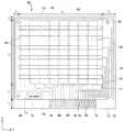
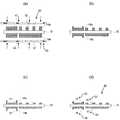
以下、図1乃至図10を参照して、本発明の実施の形態について説明する。はじめに図1を参照して、本実施の形態によるタッチパネルセンサ60全体について説明する。図1は、タッチパネルセンサ60を示す平面図である。 Hereinafter, embodiments of the present invention will be described with reference to FIGS. First, the entire
タッチパネルセンサ
タッチパネルセンサ60は、タッチパネルセンサ60への外部導体(例えば、人間の指)の接触位置または接近位置を検知して、検知に基づく信号を外部に送るものである。このタッチパネルセンサ60は、基板12と、基板12上に所定のパターンで設けられ、接触位置などのいわゆるタッチを検出する透明導電パターン61,62と、透明導電パターン61,62にそれぞれ電気的に接続された取出導電パターン63,64と、を備えている。このうち基板12の一側(例えば観察者側)には、多列に並べられ、各々がx方向に延びる複数の第1透明導電パターン61と、各第1透明導電パターン61に接続され、線状に延びる複数の第1取出導電パターン63とが設けられている。また、基板12の他側(例えば表示部側)には、多列に並べられ、各々がy方向に延びる複数の第2透明導電パターン62と、各第2透明導電パターン62に接続され、線状に延びる複数の第2取出導電パターン64とが設けられている。なお「線状に延びる」とは、図1および後述の図2A,2Bに示すように、第1取出導電パターン63および第2取出導電パターン64が、略一定の幅を有するとともに様々な方向へ引き回されている、という態様を表しているThe touch panel sensor
また、第1透明導電パターン61および第2透明導電パターン62からの信号を外部へ取り出すための第1端子部65および第2端子部66が、それぞれ第1取出導電パターン63および第2取出導電パターン64に接続されている。なお図1においては、基板12の他側に設けられている構成要素が点線で表されている。 In addition, the first
図1に示すように、基板12上の領域は、表示部(図示せず)からの映像が表示される表示領域T0であって、タッチを検出する第1透明導電パターン61および第2透明導電パターン62が配置される表示領域T0と、表示領域T0の周囲に形成され、第1取出導電パターン63および第2取出導電パターン64が配置される配線領域T1と、配線領域T1の外側に形成され、第1端子部65および第2端子部66が配置される端子領域T2と、に区画される。このうち配線領域T1および端子領域T2は、表示部からの映像が表示されない非表示領域となっている。図1に示すように、第1取出導電パターン63および第2取出導電パターン64は、配線領域T1から端子領域T2へ延びている。As shown in FIG. 1, the area on the
上述のように、第1透明導電パターン61および第2透明導電パターン62は、表示部からの映像が表示される表示領域T0に設けられている。このため、第1透明導電パターン61および第2透明導電パターン62は、導電性および透光性を有する透明導電材料から構成されている。一方、上述のように、第1取出導電パターン63、第2取出導電パターン64、第1端子部65および第2端子部66は、表示部からの映像が表示されない非表示領域に設けられている。このため、取出導電パターン63,64および端子部65,66を構成する材料が透光性を有する必要はない。従って取出導電パターン63,64および端子部65,66は一般に、透透明導電材料よりも高い電気伝導率を有し、遮光性を備えた金属材料から構成される。As described above, the first transparent
〔一側の構成要素〕
次に図1および図2Aを参照して、タッチパネルセンサ60の各構成要素のうち基板12の一側に設けられているさらなる構成要素について説明する。図2Aは、基板12の一側に設けられている構成要素を示す平面図である。[One side component]
Next, with reference to FIG. 1 and FIG. 2A, the further component provided in the one side of the board |
(シールドパターン)
図2Aに示すように、基板12の一側の配線領域T1には、所定の領域にわたって隙間無く形成された第1シールドパターン71が設けられている。この第1シールドパターン71の領域は、基板12の法線方向から見た場合に基板12の他側に設けられている上述の各第2取出導電パターン64の領域を部分的に含んでいる。例えば図1から見て取れるように、第1シールドパターン71は、各第2取出導電パターン64をほぼ全域にわたって覆うよう配置されている。このような第1シールドパターン71を設けることにより、タッチパネルセンサ60の一側において生じるノイズが基板12の他側の第2取出導電パターン64に伝達されることを防ぐことができる。例えば、指などの外部導体が基板12の一側の第1透明導電パターン61にタッチし、この際の容量変化に基づいて基板12の一側でノイズが発生したとしても、このノイズが、基板12の他側の第2取出導電パターン64に伝達されることを防ぐことができる。これによって、基板12の他側における検出の感度を向上させることができる。(Shield pattern)
As shown in FIG. 2A, the wiring region T1 of the one side of the
このような第1シールドパターン71は、好ましくは、透光性を有する材料から構成される。例えば、第1透明導電パターン61を構成する透明導電材料と同一の透明導電材料から構成される。これによって、タッチパネルセンサ60の製造工程において、第1シールドパターン71の反対側に形成される第2取出導電パターン64を視認することが可能となり、このことにより、第2取出導電パターン64の断線チェックなどを簡易に実施することができる。 Such a
フォトリソグラフィー法を用いてタッチパネルセンサ60が製造される場合、第1透明導電パターン61および第1シールドパターン71は、例えば後述する積層体の透明導電層をパターニングすることにより同時に形成される。これによって、より少ない工数で第1透明導電パターン61および第1シールドパターン71を形成することが可能となる。 When the
(ダミーパターン)
また図2Aに示すように、複数の第1取出導電パターン63のうち最も外側にある各第1取出導電パターン63のさらに外側に、第1ダミーパターン73が設けられている。この第1ダミーパターン73は、最も外側にある各第1取出導電パターン63に部分的に沿って延びるとともに、少なくとも部分的に上述の第1シールドパターン71上に位置するよう形成されている。また第1ダミーパターン73は、配線領域T1から端子領域T2へ延び、そして第1端子部75に接続されている。第1端子部75は、適切な配線(図示せず)などを介して接地されている。(Dummy pattern)
Further, as shown in FIG. 2A, a
(ダミーパターンの第1の目的)
このような第1ダミーパターン73は、第1に、各第1取出導電パターン63における寄生容量の偏差を低減するという目的のために設けられている。第2に、第1シールドパターン71を低抵抗で接地するという目的のために設けられている。はじめに、第1の目的について説明する。(First purpose of dummy pattern)
First, the
図2Aに示すように、複数の第1取出導電パターン63のうち最も外側にある各第1取出導電パターン63においては、隣接する第1取出導電パターン63が片側にしか形成されていない。このため、仮に第1ダミーパターン73が設けられていないとする場合、最も外側にある各第1取出導電パターン63において形成される静電容量は、その他の第1取出導電パターン63において形成される静電容量よりも小さくなってしまう。この場合、最も外側にある各第1取出導電パターン63に対応する第1透明導電パターン61をスキャンする際の容量検出感度が、その他の第1取出導電パターン63に対応する第1透明導電パターン61をスキャンする際の容量検出感度と異なることが考えられる。
ここで本実施の形態によれば、最も外側にある各第1取出導電パターン63のさらに外側に、第1ダミーパターン73が設けられている。このため、最も外側にある各第1取出導電パターン63において形成される静電容量と、その他の第1取出導電パターン63において形成される静電容量とをほぼ等しくすることができる。これによって、第1透明導電パターン61による検出感度が向上することが期待される。なおこのような効果は、第1ダミーパターン73のうち図2Aにおいて矢印Rにより示される範囲に対応する部分によってもたらされる。As shown in FIG. 2A, in each of the first extraction
Here, according to the present embodiment, the
このような第1ダミーパターン73は、好ましくは、第1取出導電パターン63を構成する金属材料と同一の金属材料から、第1取出導電パターン63と略同一のパターン幅で形成される。また、最も外側にある第1取出導電パターン63と第1ダミーパターン73との間の間隔は、隣接する2つの第1取出導電パターン63間の間隔と略同一となっている。これによって、寄生容量の偏差を低減するという効果をより高めることができる。 Such a
(ダミーパターンの第2の目的)
次に第2の目的について説明する。上述のように、第1ダミーパターン73は、少なくとも部分的に上述の第1シールドパターン71上に位置するよう形成されている。具体的には、第1ダミーパターン73のうち第1シールドパターン71上に設けられた部分は、第1シールドパターン71の外縁全域に沿って線状に延びるとともに、第1シールドパターン71のうちその外縁よりも内側の部分を露出させるよう形成されている。なお「露出させる」とは、図2Aに示すように、第1シールドパターン71のうちその外縁よりも内側の部分の上に第1ダミーパターン73が設けられていないということを意味している。また「露出させる」という文言は、第1ダミーパターン73以外の構成要素、例えば保護層(図示せず)などが第1シールドパターン71のうちその外縁よりも内側の部分の上に設けられることを排除するものではない。なお第1シールドパターン71の外縁全域に沿って線状に延びる第1ダミーパターン73の幅は、例えば、外縁全域にわたって均一の幅tとなっている(図2A参照)。(Second purpose of dummy pattern)
Next, the second purpose will be described. As described above, the
このような第1ダミーパターン73を設けることにより、第1ダミーパターン73を介して第1シールドパターン71を低抵抗で接地することができ、このことにより、第1シールドパターン71のシールド効果を高めることができる。また後述するように、第1ダミーパターン73が第1シールドパターン71の外縁全域に沿って線状に延びることにより、露光マスクの位置ずれが生じた場合であっても、第1シールドパターン71を常に低抵抗で接地することができる。 By providing the
〔他側の構成要素〕
次に図1および図2Bを参照して、タッチパネルセンサ60の各構成要素のうち基板12の他側に設けられているさらなる構成要素について説明する。図2Bは、基板12の他側に設けられている構成要素を示す平面図である。なお便宜上、図2Bには、基板12の一側から見た場合のパターン形状が示されている。[Components on the other side]
Next, with reference to FIG. 1 and FIG. 2B, the further component provided in the other side of the board |
(シールドパターン)
図2Bに示すように、基板12の他側の配線領域T1には、所定の領域にわたって隙間無く形成された第2シールドパターン72が設けられている。この第2シールドパターン72の領域は、基板12の法線方向から見た場合に基板12の一側に設けられている上述の各第1取出導電パターン63の領域を部分的に含んでいる。例えば図1から見て取れるように、第2シールドパターン72は、各第1取出導電パターン63をほぼ全域にわたって覆うよう配置されている。このような第2シールドパターン72を設けることにより、タッチパネルセンサ60の他側において生じるノイズが基板12の一側の第1取出導電パターン63に伝達されることを防ぐことができる。例えば、表示部から放射されるノイズが基板12の一側の第1取出導電パターン63に伝達されることを防ぐことができる。これによって、基板12の一側における検出の感度を向上させることができる。(Shield pattern)
As shown in FIG. 2B, the wiring region T1 of the other side of the
第2シールドパターン72の材料は、上述の第1シールドパターン71の場合と略同一であるので、詳細な説明は省略する。 Since the material of the
(ダミーパターン)
また図2Bに示すように、複数の第2取出導電パターン64のうち最も外側にある第2取出導電パターン64のさらに外側に、第2ダミーパターン74が設けられている。この第2ダミーパターン74は、最も外側にある各第2取出導電パターン64に部分的に沿って延びるとともに、少なくとも部分的に上述の第2シールドパターン72上に位置するよう形成されている。また第2ダミーパターン74は、配線領域T1から端子領域T2へ延び、そして第2端子部76に接続されている。第2端子部76は、適切な配線(図示せず)などを介して接地されている。(Dummy pattern)
Further, as shown in FIG. 2B, a
この第2ダミーパターン74により、上述の第1ダミーパターン73の場合と同様に、各第2取出導電パターン64における寄生容量の偏差を低減するとともに、第2シールドパターン72を低抵抗で接地することができる。なお寄生容量の偏差を低減するという効果は、第2ダミーパターン74のうち図2Bにおいて矢印Rにより示される範囲に対応する部分によってもたらされる。 As in the case of the
第2ダミーパターン74は、好ましくは、第2取出導電パターン64を構成する金属材料と同一の金属材料から、第2取出導電パターン64と略同一のパターン幅で形成される。また、最も外側にある第2取出導電パターン64と第2ダミーパターン74との間の間隔は、隣接する2つの第2取出導電パターン64間の間隔と略同一となっている。これによって、寄生容量の偏差を低減するという効果をより高めることができる。 The
また図2Bに示すように、第2ダミーパターン74のうち第2シールドパターン72上に設けられた部分は、第2シールドパターン72の外縁全域に沿って線状に延びるとともに、第2シールドパターン72のうちその外縁よりも内側の部分を露出させるよう形成されている。これによって、第1ダミーパターン73の場合と同様に、露光マスクの位置ずれが生じた場合であっても、第2シールドパターン72を常に低抵抗で接地することが可能となる。なお第2シールドパターン72の外縁全域に沿って線状に延びる第2ダミーパターン74の幅は、例えば、外縁全域にわたって均一の幅uとなっている(図2B参照)。 2B, the portion of the
タッチパネルセンサの製造方法
次に、タッチパネルセンサ60の製造方法について説明する。本実施の形態によるタッチパネルセンサ60は、フォトリソグラフィー法を用いて積層体をパターニングすることにより得られる。はじめに、用いられる積層体について説明する。Manufacturing method for a touch panel sensor Next, a method for manufacturing the
(積層体)
図3(a)は、積層体13を示す縦断面図である。また図3(b)は、フォトリソグラフィー法を用いて積層体13をパターニングすることにより得られるタッチパネルセンサ60を模式的に表す縦断面図である。(Laminate)
FIG. 3A is a longitudinal sectional view showing the
積層体13は、基板12と、基板12の一側の面上に設けられ、透明導電材料からなる第1透明導電層14と、第1透明導電層14上に設けられ、金属材料からなる第1金属層15と、第1金属層15上に設けられた光溶解型の第1感光層16と、基板12の他側の面上に設けられ、透明導電材料からなる第2透明導電層17と、第2透明導電層17上に設けられ、金属材料からなる第2金属層18と、第2金属層18上に設けられた光溶解型の第2感光層19と、を有している。 The
第1透明導電層14および第2透明導電層17を構成する透明導電材料としては、インジウム錫酸化物(ITO)、酸化亜鉛、酸化インジウム、アンチモン添加酸化錫、フッ素添加酸化錫、アルミニウム添加酸化亜鉛、カリウム添加酸化亜鉛、シリコン添加酸化亜鉛や、酸化亜鉛−酸化錫系、酸化インジウム−酸化錫系、酸化亜鉛−酸化インジウム−酸化マグネシウム系などの金属酸化物が用いられる。これらの金属酸化物が2種以上複合されてもよい。 Examples of the transparent conductive material constituting the first transparent
第1金属層15および第2金属層18を構成する金属材料としては、アルミニウム(Al)、モリブデン、パラジウム、銀(Ag)、クロム、銅等の金属及びそれらを主成分とする合金、あるいはそれら合金を含む積層体が用いられる。このうち銀を含む合金の例としては、銀、パラジウム、銅を含んでなるAPC合金が挙げられる。 Examples of the metal material constituting the
第1感光層16および第2感光層19としては、所定の光、例えば紫外線によって照射されることにより溶解する光溶解型の感光層が用いられる。 As the first
後述するように、第1取出導電パターン63、第1端子部65、第1ダミーパターン73および第1端子部75は、積層体13の第1金属層15をパターニングすることにより同時に形成される。これによって、より少ない工数で第1取出導電パターン63、第1端子部65、第1ダミーパターン73および第1端子部75を形成することが可能となる。 As will be described later, the first extraction
ところでフォトリソグラフィー法を用いて製造されたタッチパネルセンサ60においては、一般に、第1取出導電パターン63、第1端子部65、第1ダミーパターン73および第1端子部75と基板12との間に第1透明導電層14が介在されている。なぜなら、これによって、第1取出導電パターン63、第1端子部65、第1ダミーパターン73および第1端子部75における電気抵抗を、第1透明導電層14の分だけ低減することができるからである。このようにタッチパネルセンサ60において、第1取出導電パターン63、第1端子部65、第1ダミーパターン73および第1端子部75は、パターニングされた第1透明導電層14上に設けられたパターンとなっている。すなわち、本実施の形態におけるタッチパネルセンサ60は、図3(b)で模式的に示されているように、第1透明導電層14をパターニングすることにより得られる第1下側パターン20と、第1下側パターン20上に所定パターンで設けられ、第1金属層15をパターニングすることにより得られる第1上側パターン30と、を備えている。このうち第1下側パターン20には、上述の第1透明導電パターン61および第1シールドパターン71が含まれている。また第1上側パターン30には、上述の第1取出導電パターン63、第1端子部65、第1ダミーパターン73および第1端子部75が含まれている。 By the way, in the
同様に、基板12の他側に関しても、本実施の形態におけるタッチパネルセンサ60は、第2透明導電層17をパターニングすることにより得られる第2下側パターン25と、第2下側パターン25上に所定パターンで設けられ、第2金属層18をパターニングすることにより得られる第2上側パターン35と、を備えている。このうち第2下側パターン25には、上述の第2透明導電パターン62および第2シールドパターン72が含まれている。また第2上側パターン35には、上述の第2取出導電パターン64、第2端子部66、第2ダミーパターン74および第2端子部76が含まれている。 Similarly, with respect to the other side of the
(露光マスク)
次に、フォトリソグラフィー法において用いられる露光マスクについて説明する。本実施の形態においては、後述するように2回の露光工程が実施される。(Exposure mask)
Next, an exposure mask used in the photolithography method will be described. In the present embodiment, two exposure steps are performed as described later.
1回目の露光工程においては、図4Aに示す一側ファースト露光マスク40と、図4Bに示す他側ファースト露光マスク45と、が使用される。このうち一側ファースト露光マスク40は、1回目の露光工程において基板12の一側に配置される露光マスクとなっており、一方、他側ファースト露光マスク45は、1回目の露光工程において基板12の他側に配置される露光マスクとなっている。 In the first exposure process, the one-side
また2回目の露光工程においては、図5Aに示す一側セカンド露光マスク50と、図5Bに示す他側セカンド露光マスク55と、が使用される。このうち一側セカンド露光マスク50は、2回目の露光工程において基板12の一側に配置される露光マスクとなっており、一方、他側セカンド露光マスク55は、2回目の露光工程において基板12の他側に配置される露光マスクとなっている。 In the second exposure step, one side
以下、各露光マスク40,45,50,55について詳細に説明する。 Hereinafter, each of the exposure masks 40, 45, 50, and 55 will be described in detail.
〔一側ファースト露光マスク〕
はじめに一側ファースト露光マスク40について説明する。一側ファースト露光マスク40は、光を遮蔽する遮光部41と、光を透過させる透光部42とからなっている。このうち遮光部41は、図4Aに示すように、第1感光層16のうち第1シールドパターン71に対応する領域に露光光が照射されるのを防ぐシールドパターン用遮光部43と、第1感光層16のうち第1透明導電パターン61に対応する領域に露光光が照射されるのを防ぐ透明導電パターン用遮光部44と、を含んでいる。また図4Aに示すように、遮光部41は、第1感光層16のうち第1取出導電パターン63,第1端子部65,第1ダミーパターン73および第1端子部75に対応する領域に露光光が照射されるのを防ぐ部分をさらに含んでいる。すなわち遮光部41は、第1感光層16のうち上述した第1下側パターン20および第1上側パターン30に含まれる各パターンに対応する領域に露光光が照射されるのを防ぐよう形成されている。[One side first exposure mask]
First, the one-side
〔一側セカンド露光マスク〕
次に一側セカンド露光マスク50について説明する。一側セカンド露光マスク50は、光を遮蔽する遮光部51と、光を透過させる透光部52とからなっている。このうち透光部52は、図5Aに示すように、基板12の一側の感光層のうち第1シールドパターン71に対応する領域に向けて露光光を透過させるシールドパターン用透光部53と、基板12の一側の感光層のうち第1透明導電パターン61に対応する領域に向けて露光光を透過させる透明導電パターン用透光部54と、を含んでいる。なお上述のように第1シールドパターン71の領域が各第2取出導電パターン64の領域を部分的に含む場合、一側セカンド露光マスク50は、露光の際、シールドパターン用透光部53が第2取出導電パターン64となる領域を部分的に含むよう配置される。[One side second exposure mask]
Next, the one-side
なお上述のように、第1シールドパターン71上には、第1シールドパターン71の外縁全域に沿って線状に延びる第1ダミーパターン73が形成される。従って、一側セカンド露光マスク50のシールドパターン用透光部53の寸法は、第1ダミーパターン73の幅の分だけ一側ファースト露光マスク40のシールドパターン用遮光部43よりも小さくなっている。具体的には、第1ダミーパターン73の幅をtとする場合(図2A参照)、一側セカンド露光マスク50のシールドパターン用透光部53の寸法は、一側ファースト露光マスク40のシールドパターン用遮光部43の寸法よりも、x方向およびy方向においてそれぞれ2tだけ小さくなっている。また、各露光マスク40,50は、シールドパターン用遮光部43の中心とシールドパターン用透光部53の中心とが対応するよう形成されている。これによって、第1シールドパターン71の外縁全域に沿って線状に延び、幅tを有する第1ダミーパターン73を得ることができる。 As described above, the
なお本実施の形態において、第1ダミーパターン73の幅tは、起こりうる露光マスクの相対的な位置のずれの程度よりも大きくなっている。例えば、一側ファースト露光マスク40と一側セカンド露光マスク50との間で生じうる位置のずれが最大50μmである場合、第1ダミーパターン73の幅tは50μmよりも大きくなっている。これによって、仮に露光マスクの間の相対的な位置のずれが生じた場合であっても、第1シールドパターン71の外縁に沿って線状に延びる第1ダミーパターン73が途中で途切れてしまうことを防ぐことができる。 In the present embodiment, the width t of the
なお露光マスクの位置のずれとは、所定のアライメントマーク(図示せず)を基準とした場合の一側ファースト露光マスク40に対する一側セカンド露光マスク50の位置ずれだけでなく、第1シールドパターン71を基準とした場合の一側ファースト露光マスク40に対する一側セカンド露光マスク50の位置ずれも含む概念とする。従って、露光マスクの位置のずれは、各露光マスク40,50を位置決めする露光機(図示せず)のアライメント精度に起因して生じるだけでなく、一側ファースト露光マスク40を用いた露光から一側セカンド露光マスク50を用いた露光までの間に生じうる積層体13の伸縮などにも起因して生じ得る。 The displacement of the exposure mask position is not only the displacement of the one-side
〔他側ファースト露光マスク〕
次に他側ファースト露光マスク45について説明する。他側ファースト露光マスク45は、光を遮蔽する遮光部46と、光を透過させる透光部47とからなっている。このうち遮光部46は、図4Bに示すように、第2感光層19のうち第2シールドパターン72に対応する領域に露光光が照射されるのを防ぐシールドパターン用遮光部48と、第2感光層19のうち第2透明導電パターン62に対応する領域に露光光が照射されるのを防ぐ透明導電パターン用遮光部49と、を含んでいる。また図4Bに示すように、遮光部46は、第2感光層19のうち第2取出導電パターン64,第2端子部66,第2ダミーパターン74および第2端子部76に対応する領域に露光光が照射されるのを防ぐ部分をさらに含んでいる。すなわち遮光部46は、一側ファースト露光マスク40の遮光部41の場合と同様に、第2感光層19のうち上述した第2下側パターン25および第2上側パターン35に含まれる各パターンに対応する領域に露光光が照射されるのを防ぐよう形成されている。[Other side first exposure mask]
Next, the other side
〔他側セカンド露光マスク〕
次に他側セカンド露光マスク55について説明する。他側セカンド露光マスク55は、光を遮蔽する遮光部56と、光を透過させる透光部57とからなっている。このうち透光部57は、図5Bに示すように、基板12の他側の感光層のうち第2シールドパターン72に対応する領域に向けて露光光を透過させるシールドパターン用透光部58と、基板12の他側の感光層のうち第2透明導電パターン62に対応する領域に向けて露光光を透過させる透明導電パターン用透光部59と、を含んでいる。なお上述のように第2シールドパターン72の領域が各第1取出導電パターン63の領域を部分的に含んでいる場合、他側セカンド露光マスク55は、露光の際、シールドパターン用透光部58が第1取出導電パターン63となる領域を部分的に含むよう配置される。[Other side second exposure mask]
Next, the other side
なお上述のように、第2シールドパターン72上には、第2シールドパターン72の外縁全域に沿って線状に延びる第2ダミーパターン74が形成される。従って、他側セカンド露光マスク55のシールドパターン用透光部58の寸法は、第2ダミーパターン74の幅の分だけ他側ファースト露光マスク45のシールドパターン用遮光部48よりも小さくなっている。具体的には、第2ダミーパターン74の幅をuとする場合(図2B参照)、他側セカンド露光マスク55のシールドパターン用透光部58の寸法は、他側ファースト露光マスク45のシールドパターン用遮光部48の寸法よりも、x方向およびy方向においてそれぞれ2uだけ小さくなっている。また、各露光マスク45,55は、シールドパターン用遮光部48の中心とシールドパターン用透光部58の中心とが対応するよう形成されている。これによって、第2シールドパターン72の外縁全域に沿って線状に延び、幅uを有する第2ダミーパターン74を得ることができる。 As described above, on the
第2ダミーパターン74の幅uは、第1ダミーパターン73の幅tの場合と同様に、起こりうる露光マスクの相対的な位置のずれの程度よりも大きくなっている。これによって、仮に露光マスクの間の相対的な位置のずれが生じた場合であっても、第2シールドパターン72の外縁に沿って線状に延びる第2ダミーパターン74が途中で途切れてしまうことを防ぐことができる。 Similar to the case of the width t of the
(1回目のパターニング工程)
次に、露光マスク40,45,50,55を用いて積層体13をパターニングする工程について説明する。はじめに図6(a)(b)(c)(d)を参照して、一側ファースト露光マスク40および他側ファースト露光マスク45を用いる1回目のパターニング工程について説明する。なお図6(a)(b)(c)(d)に示す積層体13の縦断面図は、パターニング工程を模式的に示すためのものであり、図1乃至図2Bに示すタッチパネルセンサ60の各パターンの形状とは厳密には一致していない。(First patterning process)
Next, the process of patterning the
まず積層体13を準備する。次に図6(a)に示すように、積層体13の一側に一側ファースト露光マスク40を配置し、積層体13の他側に他側ファースト露光マスク45を配置する。 First, the laminate 13 is prepared. Next, as illustrated in FIG. 6A, the one-side
その後、第1感光層16の感光特性に対応した露光光(例えば、紫外線)を、ファースト露光マスク40を介して第1感光層16に照射する。同時に、第2感光層19の感光特性に対応した露光光(例えば、紫外線)を、他側ファースト露光マスク45を介して第2感光層19に照射する。この結果、第1感光層16および第2感光層19が、最終的に得られる第1下側パターン20および第2下側パターン25に対応したパターンで露光される。 Thereafter, the first
なお、図6(a)に示すように、積層体13において、第1感光層16と第2感光層19との間には、遮光性を有する第1金属層15および第2金属層18が介在されている。このため、積層体13の一側から照射される露光光が第2感光層19に到達することはなく、同様に、積層体13の他側から照射される露光光が第1感光層16に到達することもない。このため、第1感光層16および第2感光層19を同時に露光することが可能となっている。 As shown in FIG. 6A, in the laminate 13, between the first
次に、露光された第1感光層16および第2感光層19を現像する。これによって、図6(b)に示すように、最終的に得られる第1下側パターン20と略同一のパターンを有する一側ファースト感光パターン16aと、最終的に得られる第2下側パターン25と略同一のパターンを有する他側ファースト感光パターン19aとが形成される。 Next, the exposed first
次に、一側ファースト感光パターン16aをマスクとして、第1金属層15をエッチングする。同様に、他側ファースト感光パターン19aをマスクとして、第2金属層18をエッチングする。これによって、図6(c)に示すように、第1金属層15が一側ファースト感光パターン16aと略同一のパターンにパターニングされ、第2金属層18が他側ファースト感光パターン19aと略同一のパターンにパターニングさる。この際、エッチング液は、第1金属層15および第2金属層18を構成する材料に応じて適宜選択されるが、例えば燐酸、硝酸、酢酸および水などを所定の割合で含むエッチング液が用いられる。 Next, the
次に、一側ファースト感光パターン16aをマスクとして、第1透明導電層14をエッチングする。また、他側ファースト感光パターン19aをマスクとして、第2透明導電層17をエッチングする。これによって、図6(d)に示すように、第1透明導電層14が一側ファースト感光パターン16aと略同一のパターンにパターニングされ、第2透明導電層17が他側ファースト感光パターン19aと略同一のパターンにパターニングされる。この際、エッチング液は、第1透明導電層14および第2透明導電層17を構成する材料に応じて適宜選択されるが、例えば塩化第二鉄を含むエッチング液が用いられる。 Next, the first transparent
図7Aは、1回目のパターニング工程により得られた基板12の一側の積層パターンを示す平面図であり、図7Bは、1回目のパターニング工程により得られた基板12の他側の積層パターンを示す平面図である。図7Aに示すように、第1透明導電層14,第1金属層15および一側ファースト感光パターン16aは、第1下側パターン20および第1上側パターン30のそれぞれを包含する形状を有している。また図7Bに示すように、第2透明導電層17,第2金属層18および他側ファースト感光パターン19aは、第2下側パターン25および第2上側パターン35のそれぞれを包含する形状を有している。 7A is a plan view showing a laminated pattern on one side of the
(2回目のパターニング工程)
次に図8(a)(b)(c)(d)を参照して、一側セカンド露光マスク50および他側セカンド露光マスク55を用いる2回目のパターニング工程について説明する。なお図8(a)(b)(c)(d)に示す積層体13の縦断面図は、パターニング工程を模式的に示すためのものであり、図1乃至図2Bに示すタッチパネルセンサ60の各パターンの形状とは厳密には一致していない。(Second patterning process)
Next, with reference to FIGS. 8A, 8B, 8C, and 8D, a second patterning process using the first side
はじめに図8(a)に示すように、1回目のパターニングが実施された後の積層体13の一側に一側セカンド露光マスク50を配置し、他側に他側セカンド露光マスク55を配置する。 First, as shown in FIG. 8A, the one-side
次に露光光を、一側セカンド露光マスク50を介して一側ファースト感光パターン16aに照射する。同時に、露光光を、他側セカンド露光マスク55を介して他側ファースト感光パターン19aに照射する。この結果、一側ファースト感光パターン16aのうち第1透明導電パターン61および第1シールドパターン71に対応する部分が露光される。また、他側ファースト感光パターン19aのうち第2透明導電パターン62および第2シールドパターン72に対応する部分が露光される。 Next, the one-side first
次に、露光された一側ファースト感光パターン16aおよび他側ファースト感光パターン19aを現像する。これによって、図8(b)に示すように、最終的に得られる第1上側パターン30と略同一のパターンを有する一側セカンド感光パターン16bと、最終的に得られる第2上側パターン35と略同一のパターンを有する他側セカンド感光パターン19bと、が形成される。 Next, the exposed one side first
次に、一側セカンド感光パターン16bをマスクとして、第1透明導電層14上に残っている第1金属層15をエッチングする。同様に、他側セカンド感光パターン19bをマスクとして、第2透明導電層17上に残っている第2金属層18をエッチングする。これによって、図8(c)に示すように、第1金属層15が一側セカンド感光パターン16bと略同一のパターンにパターニングされ、第2金属層18が他側セカンド感光パターン19bと略同一のパターンにパターニングされる。この際、エッチング液としては、第1透明導電層14および第2透明導電層17をエッチングすることなく第1金属層15および第2金属層18のみを選択的にエッチングするエッチング液が用いられる。例えば燐酸、硝酸、酢酸および水などを所定の割合で含むエッチング液が用いられる。 Next, the
最後に、第1金属層15および第2金属層18上に残っている一側セカンド感光パターン16bおよび他側セカンド感光パターン19bを除去する。これによって、図8(d)に示すように、基板12と、基板12の一側の面上に所定パターンで設けられた第1下側パターン20と、第1下側パターン20上に所定パターンで設けられた第1上側パターン30と、基板12の他側の面上に所定パターンで設けられた第2下側パターン25と、第2下側パターン25上に所定パターンで設けられた第2上側パターン35と、を含むタッチパネルセンサ60が得られる。 Finally, the one-side second
(露光マスクの配置がずれる場合について)
ところで上述のように、露光マスクの位置決めの精度には限界がある。このため、上述した2回のパターニング工程において、一側ファースト露光マスク40および他側ファースト露光マスク45に対する一側セカンド露光マスク50および他側セカンド露光マスク55の相対的な位置関係がずれることが考えられる。以下、そのような相対的な位置関係のずれが生じた場合における、本実施の形態の効果について説明する。(When the exposure mask is misaligned)
As described above, there is a limit to the positioning accuracy of the exposure mask. For this reason, in the two patterning steps described above, the relative positional relationship between the one-side
なお、一側ファースト露光マスク40に対する一側セカンド露光マスク50の相対的な位置関係のずれが生じた場合における効果と、他側ファースト露光マスク45に対する他側セカンド露光マスク55の相対的な位置関係のずれが生じた場合における効果とは略同一となっている。従って、ここでは、一側ファースト露光マスク40に対する一側セカンド露光マスク50の相対的な位置関係のずれが生じた場合における効果についてのみ説明する。 It should be noted that the effect when the relative positional relationship of the one-side
図9(a)(b)(c)は、本実施の形態による第1シールドパターン71および第1ダミーパターン73を模式的に示す平面図である。このうち図9(a)は、一側ファースト露光マスク40に対する一側セカンド露光マスク50の相対的な位置ずれが無い場合に得られる第1シールドパターン71および第1ダミーパターン73を示す図である。また、図9(b)(c)は、一側ファースト露光マスク40に対する一側セカンド露光マスク50の相対的な位置ずれがy方向(図9(b)における上下方向)およびx方向(図9(c)における左右方向)に生じた場合に得られる第1シールドパターン71および第1ダミーパターン73を示す図である。 FIGS. 9A, 9B and 9C are plan views schematically showing the
はじめに、一側ファースト露光マスク40に対する一側セカンド露光マスク50の相対的な位置ずれが無い場合について説明する。この場合、図9(a)に示すように、得られる第1ダミーパターン73の幅は、第1シールドパターン71の外縁全域にわたってtとなっている。 First, a case where there is no relative displacement of the one-side
ここで、第1シールドパターン71のうち図9(a)において符号Pで示す点が、第1ダミーパターン73および第1端子部75を介して接地される経路について考える。この場合、点Pは、矢印k1で示される、右回りで第1ダミーパターン73を介して第1端子部75に到達する経路(以下、右回り経路)と、矢印k2で示される、左回りで第1ダミーパターン73を介して第1端子部75に到達する経路(以下、左回り経路)と、の2つの経路で接地されている。なお、第1シールドパターン71の電気抵抗は第1ダミーパターン73の電気抵抗に比べて大きいので、第1シールドパターン71を通って第1端子部75に到達する経路は無視されている。Here, let us consider a path in which the point indicated by symbol P in FIG. 9A in the
次に、一側ファースト露光マスク40に対する一側セカンド露光マスク50の相対的な位置ずれがy方向に生じた場合について説明する。この場合、図9(b)に示すように、露光マスクの位置ずれの分だけ、右回り経路の第1ダミーパターン73のうちx方向に延びる部分の幅が小さくなっている。一方、露光マスクの位置ずれの分だけ、左回り経路の第1ダミーパターン73のうちx方向に延びる部分の幅が大きくなっている。この結果、図9(a)に示す形態および図9(b)に示す形態において、点Pから第1ダミーパターン73を介して第1端子部75に至る経路の電気抵抗は略同一になっている。 Next, a case where a relative positional shift of the one-side
次に、一側ファースト露光マスク40に対する一側セカンド露光マスク50の相対的な位置ずれがx方向に生じた場合について説明する。この場合、図9(c)に示すように、露光マスクの位置ずれの分だけ、右回り経路の第1ダミーパターン73のうちy方向に延びる部分の幅が小さくなっている。一方、露光マスクの位置ずれの分だけ、左回り経路の第1ダミーパターン73のうちy方向に延びる部分の幅が大きくなっている。この結果、図9(a)に示す形態および図9(c)に示す形態において、点Pから第1ダミーパターン73を介して第1端子部75に至る経路の電気抵抗は略同一になっている。 Next, a case where a relative positional shift of the one-side
このように本実施の形態によれば、上述のように、透明導電材料からなる第1下側パターン20は、所定の領域にわたって隙間無く形成された第1シールドパターン71を含んでいる。また、第1下側パターン20上に形成され、金属材料からなる第1上側パターン30は、少なくとも部分的に第1シールドパターン71上に設けられた第1ダミーパターン73を含んでいる。この第1ダミーパターン73のうち第1シールドパターン71上に設けられた部分は、第1シールドパターン71の外縁全域に沿って線状に延びている。このため、一側ファースト露光マスク40に対する一側セカンド露光マスク50の相対的な位置関係がずれ、これによって第1ダミーパターン73の右回り経路が細くなったとしても、右回り経路が細くなった分だけ左回り経路が太くなるようになっている。このため、一側ファースト露光マスク40に対する一側セカンド露光マスク50の相対的な位置関係がずれた場合であっても、第1シールドパターン71を全域にわたって常に低抵抗で接地することができる。これによって、第1シールドパターン71のシールド効果を常に安定して実現することができる。 Thus, according to the present embodiment, as described above, the first
また本実施の形態によれば、第1ダミーパターン73のうち第1シールドパターン71上に設けられた部分は、第1シールドパターン71を少なくとも部分的に露出させるよう形成されている。このため、基板12の一側から他側への視認性を確保しながら、ノイズが基板の一側から他側へ、または他側から一側へ放出されるのを防ぐことができる。 According to the present embodiment, the portion of the
また本実施の形態によれば、第1シールドパターン71の外縁に沿って第1ダミーパターン73を形成することにより、第1ダミーパターン73に、第1シールドパターン71を低抵抗で接地する作用、および、第1取出導電パターン63の寄生容量の偏差を抑制する作用の両方を付与することができる。これによって、簡易な構成で効率的にタッチパネルセンサ60の特性を向上させることができる。 Further, according to the present embodiment, by forming the
なお図2Aに示すように、積層体13の第1金属層15をパターニングして第1取出導電パターン63、第1端子部65、第1ダミーパターン73および第1端子部75を形成する際、同時に第1アライメントマーク67が形成されてもよい。この第1アライメントマーク67は、例えば、タッチパネルセンサ60を表示部(図示せず)に組み合わせる際のアライメントマークとして利用される。 2A, when the
また図2Bに示すように、第2金属層18をパターニングして第2取出導電パターン64、第2端子部66、第2ダミーパターン74および第2端子部76を形成する際、同時に第2アライメントマーク68や第2ID領域70が形成されてもよい。第2アライメントマーク68は、例えば、タッチパネルセンサ60を表示部(図示せず)に組み合わせる際のアライメントマークとして利用される。また第2ID領域70は、タッチパネルセンサ60の製品名や製造番号などのID情報を表示するよう利用される。 Also, as shown in FIG. 2B, when the second extraction
比較の形態
次に、図10(a)(b)(c)を参照して、本実施の形態の効果を比較の形態と比較して説明する。図10(a)(b)(c)に示す比較の形態によるタッチパネルセンサの第1シールドパターンおよび第1ダミーパターンは、第1ダミーパターンが第1シールドパターンの片側にのみ設けられている点が異なるのみであり、他の構成は、上述の本実施の形態におけるタッチパネルセンサの第1シールドパターンおよび第1ダミーパターンと略同一である。図10(a)(b)(c)に示す比較の形態において、上述の本実施の形態と同一部分には同一符号を付して詳細な説明は省略する。Comparison Mode Next, the effects of the present embodiment will be described in comparison with the comparison mode with reference to FIGS. The first shield pattern and the first dummy pattern of the touch panel sensor according to the comparative form shown in FIGS. 10A, 10B, and 10C are such that the first dummy pattern is provided only on one side of the first shield pattern. The only difference is the other configuration, which is substantially the same as the first shield pattern and the first dummy pattern of the touch panel sensor in the present embodiment described above. In the comparison mode shown in FIGS. 10A, 10B, and 10C, the same portions as those in the above-described embodiment are denoted by the same reference numerals, and detailed description thereof is omitted.
図10(a)(b)(c)は、比較の形態による第1シールドパターン71および第1ダミーパターン173を模式的に示す平面図である。このうち図10(a)は、露光マスク間の相対的な位置ずれが無い場合に得られる第1シールドパターン71および第1ダミーパターン173を示す図である。また、図10(b)(c)は、露光マスク間の相対的な位置ずれがy方向(図10(b)における上下方向)およびx方向(図10(c)における左右方向)に生じた場合に得られる第1シールドパターン71および第1ダミーパターン173を示す図である。 FIGS. 10A, 10B, and 10C are plan views schematically showing a
図10(a)に示すように、比較の形態においては、第1ダミーパターン173が第1シールドパターン71の片側にのみ設けられている。従って、比較の形態においては、点Pは、上述の本実施の形態における右回り経路のみによって接地されている。 As shown in FIG. 10A, in the comparative form, the
次に、露光マスク間の相対的な位置ずれがy方向に生じた場合について説明する。この場合、図10(b)に示すように、露光マスクの位置ずれの分だけ、第1ダミーパターン173のうちx方向に延びる部分の幅が小さくなっている。この結果、図10(b)に示す形態においては、図10(a)に示す形態に比べて、点Pから第1ダミーパターン173を介して第1端子部75に至る経路の電気抵抗が大きくなっている。 Next, a case where relative positional deviation between exposure masks occurs in the y direction will be described. In this case, as shown in FIG. 10B, the width of the portion extending in the x direction in the
次に、露光マスク間の相対的な位置ずれがx方向に生じた場合について説明する。この場合、図10(c)に示すように、露光マスクの位置ずれの分だけ、第1ダミーパターン173のうちy方向に延びる部分の幅が小さくなっている。この結果、図10(c)に示す形態においては、図10(a)に示す形態に比べて、点Pから第1ダミーパターン173を介して第1端子部75に至る経路の電気抵抗が大きくなっている。 Next, a case where a relative positional shift between exposure masks occurs in the x direction will be described. In this case, as shown in FIG. 10C, the width of the portion extending in the y direction of the
このように比較の形態においては、露光マスク間の相対的な位置ずれの分だけ、第1シールドパターン71の接地抵抗が変動してしまうことが考えられる。 As described above, in the comparative embodiment, it is conceivable that the ground resistance of the
これに対して本実施の形態によれば、上述のように、第1ダミーパターン73のうち第1シールドパターン71上に設けられた部分は、第1シールドパターン71の外縁全域に沿って線状に延びている。このため、露光マスク間の相対的な位置ずれが生じた場合であっても、第1シールドパターン71を全域にわたって常に低抵抗で接地することができる。 On the other hand, according to the present embodiment, as described above, the portion of the
なお本実施の形態において、第1上側パターン30によってその外縁全域を囲われた第1下側パターン20が、第1ダミーパターン73によってその外縁全域を囲われた第1シールドパターン71からなる例を示した。しかしながら、これに限られることはなく、第1シールドパターン71および第1ダミーパターン73の組合せ以外にも、第1上側パターン30によってその外縁全域を囲われた第1下側パターン20が存在していてもよい。 In the present embodiment, an example in which the first
また本実施の形態において、一側ファースト露光マスク40を用いた露光と他側ファースト露光マスク45を用いた露光とが同時に実施される例を示した。しかしながら、これに限られることはなく、一側ファースト露光マスク40を用いた露光と他側ファースト露光マスク45を用いた露光とが別々に実施されてもよい。同様に、一側セカンド露光マスク50を用いた露光と他側セカンド露光マスク55を用いた露光とが別々に実施されてもよい。 In the present embodiment, the example in which the exposure using the one-side
また本実施の形態において、一側セカンド感光パターン16bが、はじめに、第1上側パターン30上に残っている一側ファースト感光パターン16aを一側セカンド露光マスク50を用いて露光し、その後、露光された一側ファースト感光パターン16aを現像することにより形成される例を示した。しかしながら、これに限られることはなく、1回目のパターニング工程の後、第1上側パターン30上に残っている一側ファースト感光パターン16aを除去し、次に、第1上側パターン30上に新たに追加で光溶解型の感光層(図示せず)を設け、その後、この追加の感光層を一側セカンド露光マスク50を用いて露光し、そして、露光された追加の感光層を現像することにより一側セカンド感光パターン16bが形成されてもよい。 In the present embodiment, the one-side second
同様に、本実施の形態において、他側セカンド感光パターン19bが、はじめに、第2上側パターン35上に残っている他側ファースト感光パターン19aを他側セカンド露光マスク55を用いて露光し、その後、露光された他側ファースト感光パターン19aを現像することにより形成される例を示した。しかしながら、これに限られることはなく、1回目のパターニング工程の後、第2上側パターン35上に残っている他側ファースト感光パターン19aを除去し、次に、第2上側パターン35上に新たに追加で光溶解型の感光層(図示せず)を設け、その後、この追加の感光層を他側セカンド露光マスク55を用いて露光し、そして、露光された追加の感光層を現像することにより他側セカンド感光パターン19bが形成されてもよい。 Similarly, in the present embodiment, the other side second
なお、第1上側パターン30上および第2上側パターン35上に新たに追加で光溶解型の感光層を設ける方法は特に限定されず、様々な公知の方法が用いられ得る。例えば、感光層の材料が溶解している感光液中に積層体13を浸漬させる方法、いわゆるディップコート法により、第1上側パターン30上および第2上側パターン35上に新たに追加で光溶解型の感光層が設けられる。なおディップコート法を用いる場合、第1上側パターン30上および第2上側パターン35上に一側ファースト感光パターン16aおよび他側ファースト感光パターン19aが残っていたとしても、積層体13が感光液中に浸漬されている間に一側ファースト感光パターン16aおよび他側ファースト感光パターン19aが感光液中に溶解され得る。すなわち、ディップコート法を用いる場合、第1上側パターン30上および第2上側パターン35上に残っている一側ファースト感光パターン16aおよび他側ファースト感光パターン19aを除去することと、第1上側パターン30上および第2上側パターン35上に新たに追加で光溶解型の感光層(図示せず)を設けることとを同時に実施することができる。またディップコート法を用いる場合、基板12の両側に同時に感光層を同時に設けることができる。従って、基板12の両側に感光層が設けられる場合、ディップコート法が好ましく用いられる。 Note that a method for newly providing a light-dissolving type photosensitive layer on the first
また上述の本実施の形態において、第1感光層16および第2感光層19として光溶解型の感光層が用いられる例を示した。しかしながら、これに限られることはなく、感光層16および第2感光層19として光硬化型の感光層が用いられてもよい。
なお光硬化型の感光層が用いられる場合、当業者にとって自明なことではあるが、各露光マスク40,45,50,55における遮光部と透光部のパターンが反転されることになる。
また光硬化型の感光層が用いられる場合、1回目のパターニング工程の後、残っている感光層が除去されることになる。その後、2回目のパターニング工程において、新たな感光層が設けられ、そしてセカンド露光マスクによって感光層が露光される。In the above-described embodiment, an example in which a photodissolvable photosensitive layer is used as the first
If a photo-curing type photosensitive layer is used, it will be obvious to those skilled in the art, but the pattern of the light-shielding part and the light-transmitting part in each of the exposure masks 40, 45, 50, 55 is reversed.
When a photocurable photosensitive layer is used, the remaining photosensitive layer is removed after the first patterning step. Thereafter, in the second patterning step, a new photosensitive layer is provided, and the photosensitive layer is exposed with a second exposure mask.
また上述の本実施の形態において、基板12の一側および他側の両方に下側パターンおよび上側パターンからなる積層パターンが形成される例を示した。しかしながら、これに限られることはなく、基板12の一側または他側の一方にのみ積層パターンが形成されていてもよい。基板12の一側または他側の一方にのみ積層パターンが形成されている場合であっても、上述の本実施の形態における技術的思想を適用することにより、下側パターンの外縁全域にわたって形成される上側パターンの抵抗値が変動することを防ぐことができる。 In the above-described embodiment, an example in which a laminated pattern including a lower pattern and an upper pattern is formed on both one side and the other side of the
また上述の本実施の形態において、第1シールドパターン71または第2シールドパターン72が、所定の領域にわたって隙間無く形成されている例を示した。すなわち、第1シールドパターン71または第2シールドパターン72がいわゆるベタ層として形成されている例を示した。しかしながら、これに限られることはなく、第1シールドパターン71または第2シールドパターン72は、ストライプ状などの様々な模様を有していてもよい。これによって、第1シールドパターン71または第2シールドパターン72は、様々な周波数のノイズに柔軟に対応することができる。従って、本実施の形態における第1シールドパターン71または第2シールドパターン72は、ノイズを遮蔽するために第1透明導電層14または第2透明導電層17が形成されている領域として定義される。 In the above-described embodiment, the example in which the
10 積層パターン基板
12 基板
13 積層体
14 第1透明導電層
15 第1金属層
16 第1感光層
17 第2透明導電層
18 第2金属層
19 第2感光層
20 第1下側パターン
25 第2下側パターン
30 第1上側パターン
35 第2上側パターン
40 一側ファースト露光マスク
41 遮光部
42 透光部
45 他側ファースト露光マスク
46 遮光部
47 透光部
50 一側セカンド露光マスク
51 遮光部
52 透光部
55 他側セカンド露光マスク
56 遮光部
57 透光部
60 タッチパネルセンサ
61 第1透明導電パターン
62 第2透明導電パターン
63 第1取出導電パターン
64 第2取出導電パターン
65 第1端子部
66 第2端子部
67 第1アライメントマーク
68 第2アライメントマーク
70 第2ID領域
71 第1シールドパターン
72 第2シールドパターン
73 第1ダミーパターン
74 第2ダミーパターン
75 第1端子部
76 第2端子部
T0 表示領域
T1 配線領域
T2 端子領域
T3 中間領域DESCRIPTION OF SYMBOLS 10 Laminated pattern board |
Claims (15)
Translated fromJapanese前記基板の一側の面上に所定パターンで設けられ、透光性および導電性を有する透明導電材料からなる第1下側パターンと、
前記第1下側パターン上に所定パターンで設けられ、遮光性および導電性を有する金属材料からなる第1上側パターンと、を備え、
前記第1下側パターンは、多列に並べられ、各々がx方向に延びる複数の第1透明導電パターンと、所定の領域にわたって形成された第1シールドパターンと、を含み、
前記第1上側パターンは、各第1透明導電パターンに接続され、線状に延びる第1取出導電パターンと、各第1取出導電パターンに接続された第1端子部と、少なくとも部分的に前記第1シールドパターン上に設けられた第1ダミーパターンと、を含み、
前記第1ダミーパターンのうち前記第1シールドパターン上に設けられた部分は、前記第1シールドパターンの外縁全域に沿って線状に延びるとともに、前記第1シールドパターンを少なくとも部分的に露出させるよう形成されていることを特徴とするタッチパネルセンサ。A substrate,
A first lower pattern that is provided in a predetermined pattern on one surface of the substrate and is made of a transparent conductive material having translucency and conductivity;
A first upper pattern that is provided in a predetermined pattern on the first lower pattern and is made of a metal material having light shielding properties and electrical conductivity;
The first lower pattern includes a plurality of first transparent conductive patterns arranged in multiple rows, each extending in the x direction, and a first shield pattern formed over a predetermined region,
The first upper pattern is connected to each of the first transparent conductive patterns, and extends in a linear manner. The first extraction conductive pattern is connected to each of the first extraction conductive patterns. The first terminal portion is connected to each of the first extraction conductive patterns. A first dummy pattern provided on one shield pattern,
A portion of the first dummy pattern provided on the first shield pattern extends linearly along the entire outer edge of the first shield pattern, and at least partially exposes the first shield pattern. A touch panel sensor that is formed.
前記第2下側パターン上に所定パターンで設けられ、遮光性および導電性を有する金属材料からなる第2上側パターンと、をさらに備え、
前記第2下側パターンは、多列に並べられ、各々がx方向に直交するy方向に延びる複数の第2透明導電パターンを含み、
前記第2上側パターンは、各第2透明導電パターンに接続され、線状に延びる第2取出導電パターンと、各第2取出導電パターンに接続された第2端子部と、を含み、
前記第1シールドパターンの領域は、前記基板の法線方向から見た場合に各第2取出導電パターンの領域を部分的に含んでいることを特徴とする請求項1に記載のタッチパネルセンサ。A second lower pattern made of a transparent conductive material provided with a predetermined pattern on the other surface of the substrate and having translucency and conductivity;
A second upper pattern that is provided in a predetermined pattern on the second lower pattern and is made of a metal material having a light shielding property and conductivity;
The second lower pattern includes a plurality of second transparent conductive patterns arranged in multiple rows, each extending in the y direction orthogonal to the x direction,
The second upper pattern includes a second extraction conductive pattern connected to each second transparent conductive pattern and extending linearly, and a second terminal portion connected to each second extraction conductive pattern,
2. The touch panel sensor according to claim 1, wherein the region of the first shield pattern partially includes a region of each second extraction conductive pattern when viewed from a normal direction of the substrate.
前記第2上側パターンは、少なくとも部分的に前記第2シールドパターン上に設けられた第2ダミーパターンをさらに含み、
前記第2ダミーパターンのうち前記第2シールドパターン上に設けられた部分は、前記第2シールドパターンの外縁全域に沿って線状に延びるとともに、前記第2シールドパターンを少なくとも部分的に露出させるよう形成されていることを特徴とする請求項2に記載のタッチパネルセンサ。The second lower pattern further includes a second shield pattern formed over a predetermined region,
The second upper pattern further includes a second dummy pattern provided at least partially on the second shield pattern,
A portion of the second dummy pattern provided on the second shield pattern extends linearly along the entire outer edge of the second shield pattern, and at least partially exposes the second shield pattern. The touch panel sensor according to claim 2, wherein the touch panel sensor is formed.
前記基板と、前記基板の一側の面上に設けられ、透明導電材料からなる第1透明導電層と、前記第1透明導電層上に設けられ、金属材料からなる第1金属層と、前記第1金属層上に設けられた光溶解型の第1感光層と、を有する積層体を準備する工程と、
遮光部と透光部とを有する一側ファースト露光マスクを用いて前記第1感光層を露光する工程と、
前記露光された第1感光層を現像して一側ファースト感光パターンを形成する工程と、
前記一側ファースト感光パターンをマスクとして前記第1透明導電層および前記第1金属層をエッチングする工程と、
パターニングされた前記第1金属層上に、光溶解型の感光層からなり、所定のパターンを有する一側セカンド感光パターンを形成する工程と、
前記一側セカンド感光パターンをマスクとして前記第1金属層をさらにエッチングする工程と、を備え、
前記一側セカンド感光パターンは、遮光部と透光部とを含む一側セカンド露光マスクを用いて光溶解型の感光層を露光することにより形成され、
前記一側ファースト露光マスクの前記遮光部は、前記第1下側パターンおよび前記第1上側パターンのそれぞれに対応する部分を含み、
前記一側セカンド露光マスクの前記透光部は、前記第1下側パターンの各第1透明導電パターンに対応する部分と、前記第1下側パターンの前記第1シールドパターンのうち露出される部分に対応する部分と、を含むことを特徴とするタッチパネルセンサの製造方法。The method of manufacturing the touch panel sensor according to claim 1,
The substrate, a first transparent conductive layer provided on one surface of the substrate and made of a transparent conductive material, a first metal layer provided on the first transparent conductive layer and made of a metal material, A step of preparing a laminate having a photodissolvable first photosensitive layer provided on the first metal layer;
Exposing the first photosensitive layer using a one-side first exposure mask having a light shielding portion and a light transmitting portion;
Developing the exposed first photosensitive layer to form a one-side first photosensitive pattern;
Etching the first transparent conductive layer and the first metal layer using the one-side first photosensitive pattern as a mask;
Forming a one-side second photosensitive pattern comprising a photodissolving photosensitive layer on the patterned first metal layer and having a predetermined pattern;
Further etching the first metal layer using the one-side second photosensitive pattern as a mask,
The one-side second photosensitive pattern is formed by exposing a photodissolvable photosensitive layer using a one-side second exposure mask including a light-shielding portion and a light-transmitting portion,
The light shielding portion of the one-side first exposure mask includes portions corresponding to the first lower pattern and the first upper pattern,
The translucent portion of the one-side second exposure mask includes a portion corresponding to each first transparent conductive pattern of the first lower pattern and an exposed portion of the first shield pattern of the first lower pattern. And a portion corresponding to the touch panel sensor.
前記第2下側パターンは、多列に並べられ、各々がx方向に直交するy方向に延びる複数の第2透明導電パターンを含み、
前記第2上側パターンは、各第2透明導電パターンに接続され、線状に延びる第2取出導電パターンと、各第2取出導電パターンに接続された第2端子部と、を含み、
前記一側セカンド露光マスクは、その透光部のうち前記第1シールドパターンの露出される部分に対応する部分が、前記基板の法線方向から見た場合に各第2取出導電パターンの領域を部分的に含むよう配置されることを特徴とする請求項7に記載のタッチパネルセンサの製造方法。The touch panel sensor is provided in a predetermined pattern on the other surface of the substrate, and includes a second lower pattern made of a transparent conductive material having translucency and conductivity, and a predetermined pattern on the second lower pattern. A second upper pattern made of a metal material having a light shielding property and conductivity,
The second lower pattern includes a plurality of second transparent conductive patterns arranged in multiple rows, each extending in the y direction orthogonal to the x direction,
The second upper pattern includes a second extraction conductive pattern connected to each second transparent conductive pattern and extending linearly, and a second terminal portion connected to each second extraction conductive pattern,
In the one-side second exposure mask, when the portion corresponding to the exposed portion of the first shield pattern in the translucent portion is viewed from the normal direction of the substrate, the region of each second extraction conductive pattern is defined. The touch panel sensor manufacturing method according to claim 7, wherein the touch panel sensor is arranged so as to partially include the touch panel sensor.
前記タッチパネルセンサの製造方法は、
遮光部と透光部とを有する他側ファースト露光マスクを用いて前記第2感光層を露光する工程と、
前記露光された第2感光層を現像して他側ファースト感光パターンを形成する工程と、
前記他側ファースト感光パターンをマスクとして前記第2透明導電層および前記第2金属層をエッチングする工程と、
パターニングされた前記第2金属層上に、光溶解型の感光層からなり、所定のパターンを有する他側セカンド感光パターンを形成する工程と、
前記他側セカンド感光パターンをマスクとして前記第2金属層をさらにエッチングする工程と、を備え、
前記他側セカンド感光パターンは、遮光部と透光部とを含む他側セカンド露光マスクを用いて光溶解型の感光層を露光することにより形成され、
前記他側ファースト露光マスクの前記遮光部は、前記第2下側パターンおよび前記第2上側パターンのそれぞれに対応する部分を含み、
前記他側セカンド露光マスクの前記透光部は、前記第2下側パターンの各第2透明導電パターンに対応する部分を含むことを特徴とする請求項8に記載のタッチパネルセンサの製造方法。The laminated body is provided on the other surface of the substrate, and a second transparent conductive layer made of a transparent conductive material, a second metal layer provided on the second transparent conductive layer and made of a metal material, A photodissolvable second photosensitive layer provided on the second metal layer,
The touch panel sensor manufacturing method includes:
Exposing the second photosensitive layer using the other-side first exposure mask having a light-shielding portion and a light-transmitting portion;
Developing the exposed second photosensitive layer to form the other side first photosensitive pattern;
Etching the second transparent conductive layer and the second metal layer using the other-side first photosensitive pattern as a mask;
A step of forming a second photosensitive pattern on the second metal layer, which is a photo-dissolving photosensitive layer and having a predetermined pattern, on the second metal layer;
Further etching the second metal layer using the other side second photosensitive pattern as a mask,
The other side second photosensitive pattern is formed by exposing a photodissolvable photosensitive layer using an other side second exposure mask including a light shielding portion and a light transmitting portion,
The light-shielding portion of the other-side first exposure mask includes portions corresponding to the second lower pattern and the second upper pattern,
9. The method of manufacturing a touch panel sensor according to claim 8, wherein the translucent portion of the other side second exposure mask includes a portion corresponding to each second transparent conductive pattern of the second lower pattern.
前記第2上側パターンは、少なくとも部分的に前記第2シールドパターン上に設けられた第2ダミーパターンをさらに含み、
前記第2ダミーパターンのうち前記第2シールドパターン上に設けられた部分は、前記第2シールドパターンの外縁全域に沿って線状に延びるとともに、前記第2シールドパターンを少なくとも部分的に露出させるよう形成されており、
前記他側セカンド露光マスクの前記透光部は、前記第2下側パターンの前記第2シールドパターンのうち露出される部分に対応する部分をさらに含むことを特徴とする請求項9に記載のタッチパネルセンサの製造方法。The second lower pattern further includes a second shield pattern formed over a predetermined region,
The second upper pattern further includes a second dummy pattern provided at least partially on the second shield pattern,
A portion of the second dummy pattern provided on the second shield pattern extends linearly along the entire outer edge of the second shield pattern, and at least partially exposes the second shield pattern. Formed,
The touch panel as set forth in claim 9, wherein the translucent portion of the other side second exposure mask further includes a portion corresponding to an exposed portion of the second shield pattern of the second lower pattern. Sensor manufacturing method.
Priority Applications (1)
| Application Number | Priority Date | Filing Date | Title |
|---|---|---|---|
| JP2011066390AJP5168377B2 (en) | 2011-03-24 | 2011-03-24 | Touch panel sensor and method for manufacturing touch panel sensor |
Applications Claiming Priority (1)
| Application Number | Priority Date | Filing Date | Title |
|---|---|---|---|
| JP2011066390AJP5168377B2 (en) | 2011-03-24 | 2011-03-24 | Touch panel sensor and method for manufacturing touch panel sensor |
Related Child Applications (1)
| Application Number | Title | Priority Date | Filing Date |
|---|---|---|---|
| JP2012281491ADivisionJP5699357B2 (en) | 2012-12-25 | 2012-12-25 | Touch panel sensor and method for manufacturing touch panel sensor |
Publications (2)
| Publication Number | Publication Date |
|---|---|
| JP2012203565A JP2012203565A (en) | 2012-10-22 |
| JP5168377B2true JP5168377B2 (en) | 2013-03-21 |
Family
ID=47184534
Family Applications (1)
| Application Number | Title | Priority Date | Filing Date |
|---|---|---|---|
| JP2011066390AExpired - Fee RelatedJP5168377B2 (en) | 2011-03-24 | 2011-03-24 | Touch panel sensor and method for manufacturing touch panel sensor |
Country Status (1)
| Country | Link |
|---|---|
| JP (1) | JP5168377B2 (en) |
Families Citing this family (8)
| Publication number | Priority date | Publication date | Assignee | Title |
|---|---|---|---|---|
| CN103376928B (en)* | 2012-04-17 | 2017-04-19 | 宸鸿科技(厦门)有限公司 | Touch panel and production method thereof |
| JP6122672B2 (en)* | 2013-03-19 | 2017-04-26 | グンゼ株式会社 | Projection Capacitance Type Touch Panel Film Manufacturing Method |
| WO2015155944A1 (en)* | 2014-04-09 | 2015-10-15 | パナソニックIpマネジメント株式会社 | Touch sensor |
| WO2016039106A1 (en)* | 2014-09-08 | 2016-03-17 | 富士フイルム株式会社 | Conductive film for touch panel |
| JP5989757B2 (en) | 2014-12-26 | 2016-09-07 | 日本写真印刷株式会社 | Touch panel |
| JP6027633B2 (en)* | 2015-01-13 | 2016-11-16 | 日本写真印刷株式会社 | Method for manufacturing touch input sensor and photosensitive conductive film |
| TWI637297B (en)* | 2015-02-27 | 2018-10-01 | 日商藤倉股份有限公司 | Wiring body, wiring board, and touch detector |
| JP2019079081A (en)* | 2016-03-11 | 2019-05-23 | アルプスアルパイン株式会社 | Capacitive sensor |
Family Cites Families (2)
| Publication number | Priority date | Publication date | Assignee | Title |
|---|---|---|---|---|
| JP5306059B2 (en)* | 2009-05-29 | 2013-10-02 | 株式会社ジャパンディスプレイウェスト | Touch panel, display panel, touch panel substrate, display panel substrate, and display device |
| JP5300640B2 (en)* | 2009-07-27 | 2013-09-25 | 株式会社ジャパンディスプレイウェスト | Capacitance type input device and electro-optical device with input device |
- 2011
- 2011-03-24JPJP2011066390Apatent/JP5168377B2/ennot_activeExpired - Fee Related
Also Published As
| Publication number | Publication date |
|---|---|
| JP2012203565A (en) | 2012-10-22 |
Similar Documents
| Publication | Publication Date | Title |
|---|---|---|
| JP5168377B2 (en) | Touch panel sensor and method for manufacturing touch panel sensor | |
| JP5699357B2 (en) | Touch panel sensor and method for manufacturing touch panel sensor | |
| JP5892419B2 (en) | Touch panel sensor | |
| TWI543035B (en) | Touch screen panel and fabricating method thereof | |
| KR101464818B1 (en) | Capacitance type input device and production method thereof | |
| EP2737390B1 (en) | Capacitive touch panel and a method of manufacturing the same | |
| US8614403B2 (en) | Electrostatic capacitance type input device | |
| EP2209065A2 (en) | Touch screen panel and method for fabricating the same | |
| KR102052165B1 (en) | Method for manufacturing a touch screen panel | |
| CN101553776A (en) | Touch panel apparatus and method for manufacturing the same | |
| CN105359071A (en) | Touch sensor and method for manufacturing touch sensor | |
| JP2011146023A (en) | Touch panel | |
| JP5892418B2 (en) | Touch panel sensor, touch panel sensor manufacturing method, and laminate for manufacturing touch panel sensor | |
| US9158343B2 (en) | Touch panel and method of fabricating the same | |
| CN112259564A (en) | Display panel, preparation method thereof and display device | |
| TW201715356A (en) | Touch panel and manufacturing method thereof | |
| JP5979473B2 (en) | Conductive pattern substrate, touch panel sensor, method for manufacturing conductive pattern substrate, and method for manufacturing touch panel sensor | |
| WO2013191024A1 (en) | Touch panel, display apparatus provided with touch panel, and method for manufacturing touch panel | |
| JP5652717B2 (en) | Method for manufacturing laminated pattern substrate and method for manufacturing touch panel sensor | |
| JP2017004519A (en) | Conductive pattern substrate | |
| CN104731397A (en) | Touch panel and touch display device | |
| CN112394844A (en) | Touch substrate and touch display device | |
| US10976879B2 (en) | Method of manufacturing a touch panel and touch panel | |
| JP6205995B2 (en) | Display device with touch panel sensor and touch position detection function | |
| KR20160048288A (en) | Touch Screen Panel and Fabricating Method Thereof |
Legal Events
| Date | Code | Title | Description |
|---|---|---|---|
| A621 | Written request for application examination | Free format text:JAPANESE INTERMEDIATE CODE: A621 Effective date:20121025 | |
| A871 | Explanation of circumstances concerning accelerated examination | Free format text:JAPANESE INTERMEDIATE CODE: A871 Effective date:20121025 | |
| A975 | Report on accelerated examination | Free format text:JAPANESE INTERMEDIATE CODE: A971005 Effective date:20121115 | |
| TRDD | Decision of grant or rejection written | ||
| A01 | Written decision to grant a patent or to grant a registration (utility model) | Free format text:JAPANESE INTERMEDIATE CODE: A01 Effective date:20121127 | |
| A61 | First payment of annual fees (during grant procedure) | Free format text:JAPANESE INTERMEDIATE CODE: A61 Effective date:20121210 | |
| R150 | Certificate of patent or registration of utility model | Ref document number:5168377 Country of ref document:JP Free format text:JAPANESE INTERMEDIATE CODE: R150 | |
| RD02 | Notification of acceptance of power of attorney | Free format text:JAPANESE INTERMEDIATE CODE: R3D02 | |
| LAPS | Cancellation because of no payment of annual fees |