JP5166085B2 - Light emitting diode - Google Patents
Light emitting diodeDownload PDFInfo
- Publication number
- JP5166085B2 JP5166085B2JP2008070328AJP2008070328AJP5166085B2JP 5166085 B2JP5166085 B2JP 5166085B2JP 2008070328 AJP2008070328 AJP 2008070328AJP 2008070328 AJP2008070328 AJP 2008070328AJP 5166085 B2JP5166085 B2JP 5166085B2
- Authority
- JP
- Japan
- Prior art keywords
- wavelength range
- light
- active region
- radiation
- conversion element
- Prior art date
- Legal status (The legal status is an assumption and is not a legal conclusion. Google has not performed a legal analysis and makes no representation as to the accuracy of the status listed.)
- Expired - Fee Related
Links
Images


Classifications
- H—ELECTRICITY
- H10—SEMICONDUCTOR DEVICES; ELECTRIC SOLID-STATE DEVICES NOT OTHERWISE PROVIDED FOR
- H10H—INORGANIC LIGHT-EMITTING SEMICONDUCTOR DEVICES HAVING POTENTIAL BARRIERS
- H10H20/00—Individual inorganic light-emitting semiconductor devices having potential barriers, e.g. light-emitting diodes [LED]
- H10H20/80—Constructional details
- H10H20/85—Packages
- H10H20/851—Wavelength conversion means
- H10H20/8511—Wavelength conversion means characterised by their material, e.g. binder
- H10H20/8512—Wavelength conversion materials
- H10H20/8513—Wavelength conversion materials having two or more wavelength conversion materials
- F—MECHANICAL ENGINEERING; LIGHTING; HEATING; WEAPONS; BLASTING
- F21—LIGHTING
- F21K—NON-ELECTRIC LIGHT SOURCES USING LUMINESCENCE; LIGHT SOURCES USING ELECTROCHEMILUMINESCENCE; LIGHT SOURCES USING CHARGES OF COMBUSTIBLE MATERIAL; LIGHT SOURCES USING SEMICONDUCTOR DEVICES AS LIGHT-GENERATING ELEMENTS; LIGHT SOURCES NOT OTHERWISE PROVIDED FOR
- F21K9/00—Light sources using semiconductor devices as light-generating elements, e.g. using light-emitting diodes [LED] or lasers
- H—ELECTRICITY
- H10—SEMICONDUCTOR DEVICES; ELECTRIC SOLID-STATE DEVICES NOT OTHERWISE PROVIDED FOR
- H10H—INORGANIC LIGHT-EMITTING SEMICONDUCTOR DEVICES HAVING POTENTIAL BARRIERS
- H10H29/00—Integrated devices, or assemblies of multiple devices, comprising at least one light-emitting semiconductor element covered by group H10H20/00
- H10H29/10—Integrated devices comprising at least one light-emitting semiconductor component covered by group H10H20/00
- H10H29/14—Integrated devices comprising at least one light-emitting semiconductor component covered by group H10H20/00 comprising multiple light-emitting semiconductor components
Landscapes
- Led Device Packages (AREA)
Description
Translated fromJapanese本発明は、発光ダイオードに関し、具体的には、所望の色温度の白色光を生成する発光ダイオードに関する。 The present invention relates to a light emitting diode, and more particularly to a light emitting diode that generates white light having a desired color temperature.
発光ダイオード(LED)は、電気的に順方向にバイアスをかけたときに、狭いスペクトルのインコヒーレント光を放射する半導体デバイスである。この作用は、エレクトロルミネッセンス型である。放射される光の色は、使用される半導体材料の組成及び状態に依存し、赤外、可視又は近紫外とすることができる。通常のダイオードと同様に、LEDは不純物を注入又はドープしてp−n接合を形成する半導体材料のチップで構成されるが、p−n接合では電流はp側又はアノードから、n側又はカソードに容易に流れ、逆方向には流れない。電子及び正孔である電荷担体は、異なる電圧を有する電極から接合内に流入する。電子は正孔と出会うと低エネルギー準位に落ち、光子の形態でエネルギーを放出する。 Light emitting diodes (LEDs) are semiconductor devices that emit narrow spectrum incoherent light when electrically forward biased. This action is of the electroluminescence type. The color of the emitted light depends on the composition and state of the semiconductor material used and can be infrared, visible or near ultraviolet. Like a normal diode, an LED is composed of a chip of semiconductor material in which an impurity is implanted or doped to form a pn junction, where current flows from the p side or anode to the n side or cathode. Flows easily, but not in the reverse direction. Charge carriers, which are electrons and holes, flow into the junction from electrodes having different voltages. When an electron meets a hole, it falls to a low energy level and emits energy in the form of photons.
LEDは、最初にガリウムヒ素から作られた赤外及び赤色デバイスを用いて開発された。しかし、材料科学の進歩は、絶えずより短波長のデバイスの製造を可能にし、様々な色の光を生成している。従来、LEDは、その表面上に堆積したp型層に結合した電極を有するサファイアのようなn型基板の上に作成される。一方、あまり一般的ではないp型基板がなお生ずることもある。放射される波長に対して透明であり、放射が反射層によって戻されるような基板は、LED効率を高める。パッケージ材料の屈折率は半導体の屈折率に適合する必要がある。LEDの欠点は、生成された光が部分的に半導体内に反射して戻り、そこで吸収され、付加的な熱に変化することである。 LEDs were originally developed using infrared and red devices made from gallium arsenide. However, advances in material science are constantly enabling the production of shorter wavelength devices, producing light of various colors. Conventionally, LEDs are made on an n-type substrate, such as sapphire, having electrodes bonded to a p-type layer deposited on its surface. On the other hand, less common p-type substrates may still occur. A substrate that is transparent to the emitted wavelength and whose radiation is returned by the reflective layer increases the LED efficiency. The refractive index of the package material needs to match the refractive index of the semiconductor. The disadvantage of LEDs is that the light produced is partially reflected back into the semiconductor where it is absorbed and converted into additional heat.
白色LEDの一実施形態は特許文献1に開示されている。白色発光ダイオード(LED)は、青色又は紫外LEDダイの発光経路上に適切な角度で配置された反射鏡を含む。蛍光体を反射鏡面、LEDの発光面、又はその両方にコーティングし、その結果、LEDダイにより放射される青色又は紫外光により蛍光体が励起され、白色光を生成する。白色LEDは長い寿命を有し、そして、LEDダイから蛍光体を離してLEDから放射される光が蛍光体に幾つかの励起過程を行わせることを可能にすることによって、均一な光色を有する。 One embodiment of a white LED is disclosed in US Pat. White light emitting diodes (LEDs) include reflectors disposed at appropriate angles on the light emission path of a blue or ultraviolet LED die. The phosphor is coated on the reflecting mirror surface, the light emitting surface of the LED, or both so that the phosphor is excited by the blue or ultraviolet light emitted by the LED die to produce white light. White LEDs have a long lifetime and provide a uniform light color by separating the phosphor from the LED die and allowing the light emitted from the LED to cause the phosphor to undergo several excitation processes. Have.
典型的には、単一のLEDからの光が不十分である用途において、照明をもたらすためには数個のLEDを寄せ集める必要がある。これは例えば、ディスプレイを照明するために白色LEDの個数に頼るディスプレイのような、バックライト装置の場合である。種々異なる作業を実施するためのあらゆる種類のデバイスにおいて、LEDが都合よく使用されることは、当業者には明らかであろう。特に、それらは、デジタル・クロック上の数字を形成し、リモート・コントロールから情報を伝達し、時計を照らし出し、そして電気器具が使用するのにいつ作動するかを表示する。一緒に集まると、それらは、ラップトップ・コンピュータ、電子手帳、携帯電話、テレビジョン・スクリーンなどのディスプレイ上に画像を形成し、或いは、交通信号灯を明るくすることさえできる。そのため、このようなデバイス及び/又はディスプレイは、均一な色温度を示すことが好ましい。しかし、白色光を発生する蛍光体でコーティングされた特定の型のLED、いわゆる白色LEDは、原材料源、結晶成長、取扱い、原材料の保管状態、及び製造プロセス内の他の変数における違いのために色温度の変動を示す。そのため、製造されるLEDは、ディスプレイのバックライト装置内にアセンブルする前にビン貯蔵する必要がある。ビン貯蔵する方法は、典型的には、カラー座標又は相関色温度(CCT)を用いてLEDを分類するが、同じCCTを有するLEDがなお異なる色彩を有する可能性がある。製造者は、それぞれのビン内のLEDのバラツキを低減するための新たなビン貯蔵方式を用いてきた。このようなビン貯蔵プロセスは、LEDの製造コストを著しく増加させる。 Typically, in applications where light from a single LED is inadequate, several LEDs need to be brought together to provide illumination. This is the case for backlight devices, for example displays that rely on the number of white LEDs to illuminate the display. It will be apparent to those skilled in the art that LEDs are conveniently used in all types of devices to perform different tasks. In particular, they form numbers on the digital clock, communicate information from the remote control, illuminate the clock, and indicate when the appliance is activated for use. When gathered together, they can form images on displays such as laptop computers, electronic notebooks, cell phones, television screens, or even light traffic lights. As such, such devices and / or displays preferably exhibit a uniform color temperature. However, certain types of LEDs coated with phosphors that generate white light, so-called white LEDs, are due to differences in raw material sources, crystal growth, handling, raw material storage conditions, and other variables within the manufacturing process. Indicates the variation in color temperature. Therefore, the manufactured LEDs need to be binned before assembling into the display backlight device. Bin storage methods typically classify LEDs using color coordinates or correlated color temperature (CCT), but LEDs with the same CCT may still have different colors. Manufacturers have used new bin storage schemes to reduce LED variability within each bin. Such a bin storage process significantly increases the manufacturing cost of the LED.
従って、1つ又は複数の上述の欠点を改善した白色光を与えることのできる改良されたLEDを提供する必要がある。所望の色温度の白色光を生成することのできる改良されたLEDを提供する方法、及び、改良されたLEDを用いて所望の色点の白色光を生成する方法がなければ、この技術の有望性は、決して完全に達成することはできない。 Accordingly, there is a need to provide an improved LED that can provide white light that improves one or more of the above-mentioned drawbacks. The pros of this technology would be without a method of providing an improved LED capable of producing white light of a desired color temperature and a method of producing white light of a desired color point using the improved LED. Sex can never be achieved completely.
従って、本発明は、第1の波長範囲に入る放射を生成する活性領域を有する発光ダイオードを提供する。活性領域の第1の部分は、第1波長範囲に入る放射を第2の波長範囲に入る放射に変換する第1の変換要素によって覆われる。活性領域の残りの第2の部分は、第1波長範囲に入る放射を第3の波長範囲に入る放射に変換する第2の変換要素によって覆われる。発光ダイオードは、第1波長範囲に入る放射の強度を制御して、第2波長範囲及び第3波長範囲に入る放射を混合することによって生成される白色光の色点を制御するように構成される。LED100は、液晶ディスプレイ・デバイスのようなディスプレイ・デバイスを照らし出すためのバックライト装置内にアセンブルするのに都合よく用いることができ、ディスプレイ・パネルを照明するが、そこでは使用用途に応じてディスプレイ上の読み易さ及び視程を改善するために調節可能な色温度及び高いコントラストを与えることができる。LEDは、所望の色点を有する白色光を必要とするランプ内にアセンブルするのに都合よく用いることができる。 Accordingly, the present invention provides a light emitting diode having an active region that generates radiation that falls within a first wavelength range. The first portion of the active region is covered by a first conversion element that converts radiation that falls within the first wavelength range into radiation that falls within the second wavelength range. The remaining second portion of the active region is covered by a second conversion element that converts radiation that falls within the first wavelength range into radiation that falls within the third wavelength range. The light emitting diode is configured to control the color point of white light generated by controlling the intensity of radiation entering the first wavelength range and mixing radiation entering the second wavelength range and the third wavelength range. The The
本発明のさらなる態様によると、発光ダイオードから白色光を生成する方法であって、活性領域によって生成された第1波長範囲に入る放射を、第1変換要素によって第2波長範囲に入る放射に実質的に変換し、活性領域によって生成された第1波長範囲に入る放射を、第2変換要素によって第3波長範囲に入る放射に実質的に変換し、次いで、第2波長範囲に入る放射と第3波長範囲に入る放射を混合して白色光を生成することによって、白色光を生成する方法が提供される。その結果、発光ダイオードの活性領域に供給されるバイアスを制御装置により適切に調整して、第1波長範囲に入る放射の強度を制御し、所望の色点を有する白色光を生成することができる。 According to a further aspect of the present invention, a method for generating white light from a light emitting diode, wherein the radiation entering the first wavelength range generated by the active region is substantially converted to radiation entering the second wavelength range by the first conversion element. Radiation that enters the first wavelength range generated by the active region is substantially converted by the second conversion element into radiation that enters the third wavelength range, and then radiation that enters the second wavelength range A method of generating white light is provided by mixing radiation that falls within the three wavelength range to generate white light. As a result, the bias supplied to the active region of the light emitting diode can be appropriately adjusted by the control device to control the intensity of the radiation entering the first wavelength range and to generate white light having a desired color point. .
本発明のこれらの及びさらなる態様は、添付の図面を参照しながら以下に説明する実施形態から明らかとなり、この実施形態に関連して明らかにすることになる。図面は、本発明の実施形態を示し、記述とともに、本発明の原理をさらに説明するために役立つ。 These and further aspects of the invention will be apparent from and elucidated with reference to the embodiments described hereinafter with reference to the accompanying drawings. The drawings illustrate embodiments of the invention and, together with the description, serve to further explain the principles of the invention.
図1は、本開示による発光ダイオード100の内部の例示的な実施形態を示す。発光ダイオード100(以後、LEDとも呼ぶ)は、例えばサファイア又は基板を形成するのに用いられる任意の他の適切な材料の基板110を含み、この基板に共通のカソード115が結合し、カソード115はさらに制御装置160に結合する。活性領域120、例えばGaAs、AlGaAs、GaP、GaAsPなどの半導体合金は、第1波長範囲150、典型的には赤色波長範囲に入る放射を与えるが、基板110の上に形成される。赤色波長範囲内の放射を与えるこのようなLEDは、比較的低コストで製造することが容易である。アノード117は活性領域120に結合し、そしてアノード117は制御装置160に結合し、典型的には、電子/電気回路がLEDを駆動する電流を供給する。制御装置160、及びカソード115とアノード117を接続するコネクタ(図示せず)は、随意の要素である。コネクタにより設けられるカソード及びアノードと制御装置との接続は、当業者にはよく知られている。LED110は、典型的には制御装置160及びコネクタなしに、製造され販売される。 FIG. 1 illustrates an exemplary embodiment inside a
活性領域120は、p−n接合を形成するドープ半導体であり、LEDを駆動するために必要な電流を供給するアノード117を介して共通の制御装置160に接続される。電流は、アノード117(p側)からカソード115(n側)へ流れる。電荷担体、即ち電子及び正孔は、異なる電圧を有する電極115、117から接合内に流入する。電子が正孔に出会うとき、電子は、典型的には低エネルギー準位に落ち、その結果、光子の形態でエネルギーを放出する。活性領域120は、エピタキシ、エッチング又は類似の方法を用いて、単一の基板110の上、又は独立したそれぞれの基板の上に同様に形成することができる。順方向バイアスが印加されるとき、電位差は活性領域に可視スペクトルの赤色及び/又は近赤外の波長範囲内の放射を生じさせることが好ましい。 The
活性領域120は、バイアスを印加されるとき第1波長範囲150に入る放射(可視スペクトルの赤色又は近赤外波長範囲内にピークを有し、600nm又はそれ以上のピーク波長を有し、以後、赤色光と呼ぶ)を与える。活性領域120の第1の部分121は、第1変換要素130で覆われ、この第1変換要素は、アップ・コンバートする蛍光体又はアップ・コンバートする量子ドットであり、第1波長範囲150に入る放射を、第2波長範囲152に入る放射に完全に変換することができる。第2波長範囲152に入る変換された放射は、可視スペクトルの青色の波長範囲(以後、青色光と呼ぶ)に入る。活性領域120の残りの第2の部分122は、第2変換要素140で覆われ、典型的には、アップ・コンバートする蛍光体又はアップ・コンバートする量子ドットであり、第1波長範囲150に入る放射を、可視スペクトルの黄色の波長範囲に入る第3波長範囲154に入る放射に(以後、黄色光と呼ぶ)完全に変換することができる。従って、第1変換要素130は、赤色光150を青色光152に完全に変換し、第2変換要素140は、赤色光150を黄色光154に完全に変換する。1つより多くの組合せの蛍光体を用いて異なる色の光を生成できることは、当業者には明らかであろう。例えば、一実施形態において、活性領域120の一部分は露出したままにすることができ、活性領域の一部分は赤色光を青色光に変換する蛍光体で覆うことができ、活性領域の残りの部分は赤色光を緑色光(黄緑色光)に変換する蛍光体で覆うことができるので、赤色光、青色光及び緑色光を混合して、赤色光の放射強度を制御することにより所望の色点の白色光を生成することができる。 The
蛍光体130、140及び/又は量子ドットは、それらが活性領域からの放射である赤色光150を、それぞれの青色波長範囲152(青色光)及びそれぞれの黄色波長範囲154(黄色光)に完全にアップ・コンバートするように選択される。赤色光を青色光及び黄色光に完全に変換するために、第1変換要素130及び第2変換要素140の厚さは、赤色光150である活性領域からの全放射が青色光152及び黄色光154に変換されるように選択される。例えば、一実施形態において、Er、Ybドープ・イットリウムをベースとするナノサイズ蛍光体が、赤色光を青色光及び/又は黄色光にアップ・コンバートするためのアップ・コンバート蛍光体として有利に使用される。活性領域120から放射された赤色光150を、変換要素130、140を用いて完全に変換するためには、変換要素の厚さは、特に変換要素が蛍光体であるとき重要な要素である。量子ドットを蛍光体の代わりに用いるときは、量子ドットの薄いコーティング膜は、ある波長から別の波長に光を完全に変換することが可能でなければならない。蛍光体又は量子ドットのいずれかを用いるとき、その厚さは、赤色光を青色光及び黄色光に完全に変換するのに実質的に十分でなければならない。しかし、量子ドットの出力効率は蛍光体に比べて低く、そのため蛍光体が好ましいことは、当業者には明らかであろう。蛍光体の厚さは、全赤色光が第1変換要素130によって青色光に変換され、また全赤色光が第2変換要素140によって黄色光に変換されるように、最適に選択する必要がある。次に、青色光152及び黄色光154は適切に混合して白色光を生成することができ、その際、白色光の色点は、活性領域に供給される電流を制御し、それゆえ赤色光150の強度を制御することによって調整することができる。
さらに進んだ実施形態において、発光ダイオード100の電極115、117は、制御装置160に結合されるが、この装置は、第1波長範囲に入る放射の強度を制御するように構成され、可変抵抗器により活性領域120に供給される電流を調節して放射される赤色光の強度を調節することができる。活性領域に供給される電流を制御することによって、第2波長範囲152及び第3波長範囲154に入る放射を混合して生成した白色光の色点は、デバイスと使用用途に応じて適切に制御することができる。 In a further advanced embodiment, the
アノード、カソードなどのコネクタ及び、LED内に用いられる全てのワイヤ・ボンドは、同じ導電性金属で形成して同じ電気的及び熱的特性を有するようにし、異なる材料を用いた状態に比べて改善された導電性をもたらすことが好ましい。さらに進んだ実施形態においては、活性領域に供給する電圧を独立に制御することができて、所望の色温度の混合白色光が得られることが好ましい。活性領域に供給する電流を調節することによって、第1波長範囲に入る放射の強度又はエネルギーは、容易に調節することができ、従って白色点の色温度を適切に調整することができる。その結果、可変の色温度を有する光源を、この単純な構造体を用いて実現することができる。これは、黄色発光蛍光体の光度が、本質的に青色発光蛍光体の光度と相関するためである。従って、活性領域の光度を適切に制御することによって、LEDに任意の色温度の白色光を生成させることができる。 Connectors such as anodes, cathodes, and all wire bonds used in LEDs are made of the same conductive metal to have the same electrical and thermal properties, which is an improvement over using different materials It is preferable to provide improved conductivity. In a further advanced embodiment, it is preferable that the voltage supplied to the active region can be controlled independently and mixed white light with a desired color temperature is obtained. By adjusting the current supplied to the active region, the intensity or energy of radiation entering the first wavelength range can be easily adjusted, and thus the color temperature of the white point can be adjusted appropriately. As a result, a light source having a variable color temperature can be realized using this simple structure. This is because the luminous intensity of the yellow-emitting phosphor is essentially correlated with the luminous intensity of the blue-emitting phosphor. Therefore, by appropriately controlling the luminous intensity of the active region, the LED can generate white light having an arbitrary color temperature.
図2は、単一の基板110の上に形成されたLED101の例示的な実施形態を示す。第1活性領域122が基板の第1の部分の上に形成され、第2活性領域124が基板110の第2の部分の上に形成される。活性領域122、124の両方は、外部制御装置(図示せず)に結合し、活性領域のそれぞれに供給する電流は、独立に適切に調整することができる。第1活性領域122は、第1波長範囲150内の放射(赤色光)を第2波長範囲152に入る放射(青色光)に完全に変換する第1変換要素130によって覆われる。第2活性領域124は、第1波長範囲150内の放射(赤色光)を第3波長範囲154に入る放射(黄色光)に完全に変換する第2変換要素によって覆われる。青色光152及び黄色光154は混合されて白色光を生成する。白色光の色点は、第1活性領域122及び第2活性領域124のそれぞれに独立に供給する電流を独立に制御することによって適切に調整することができる。活性領域及び変換要素(蛍光体)の全ての他の機能の詳細は、図1に関して前述したのと同じである。 FIG. 2 illustrates an exemplary embodiment of the LED 101 formed on a
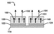
図3は、分離した基板の上に形成されたLED102の例示的な実施形態を示す。第1活性領域122が第1基板112の上に形成され、第2活性領域124が第2基板114の上に形成される。第1基板112及び第2基板114は、共通の電極115の上に取り付けられる。活性領域122、124の両方は、外部制御装置(図示せず)に結合し、活性領域のそれぞれに供給する電流は、独立に適切に調整することができる。第1活性領域122は、第1波長範囲150内の放射(赤色光)を第2波長範囲152に入る放射(青色光)に完全に変換する第1変換要素130によって覆われる。第2活性領域124は、第1波長範囲150内の放射(赤色光)を第3波長範囲154に入る放射(黄色光)に完全に変換する第2変換要素によって覆われる。青色光152及び黄色光154は混合されて白色光を生成する。白色光の色点は、第1活性領域122及び第2活性領域124のそれぞれに独立に供給する電流を独立に制御することによって適切に調整することができる。活性領域及び変換要素(蛍光体)の全ての他の機能の詳細は、図1に関して前述したのと同じである。 FIG. 3 illustrates an exemplary embodiment of the
図4は、本明細書に開示される白色LEDの実施形態100に関するスペクトル200の例示的な実施形態を示す。x軸は、LEDの活性領域によって生成された発光スペクトル及びLEDの変換されたスペクトルの波長を表し、y軸は発光強度を表す。白色LEDは、第1波長範囲250に入る発光を与え、これは約600nm又はそれ以上の波長にピークを有し、可視スペクトルの赤色/近赤外部分に入る。発光250のピークにおける両方向の矢印は、図1の前述された制御装置によって発光強度を制御できることを示している。活性領域から放射された赤色光250は、第1変換要素により青色光252に、また第2変換要素により黄色光254に、それぞれ完全に変換される。青色光252及び黄色光254は混合して白色光を生成することができる。青色光及び黄色光を混合して白色光を生成することは、当業者には周知のことである。白色光の色点は、赤色光の発光強度を制御することによって適切に調整することができる。 FIG. 4 shows an exemplary embodiment of a
図5は、白色LED102に関するスペクトル200の例示的な実施形態を示す。x軸は放射の波長を表し、y軸は発光スペクトルの強度を表す。第1活性領域は赤色波長範囲250A内の放射を生成し、第2活性領域は赤色波長範囲250B内の放射を生成する。説明のために、2つのピークは互いに並んで示されている。第1変換要素は赤色光250Aを青色光252に完全に変換し、第2変換要素は赤色光250Bを黄色光254に完全に変換する。青色光252及び黄色光254は適切に混合して白色光を生成することができる。白色光の色温度は、赤色光250A及び/又は250Bの発光強度を適切に変化させることによって選択することができる。説明のために、青色光252の放射は、黄色光254の放射よりもやや強く示している。青色光252の強度が高いほど、相関色温度、従って色点が高くなることは利点である。 FIG. 5 shows an exemplary embodiment of
前述したように、第1活性領域122及び第2活性領域124への電流は独立に制御することができ、そのためこれらの活性領域からの発光強度を独立に調節することができる。青色光のスペクトルのピーク及び黄色光のスペクトルのピークにある両方向の矢印は、第1活性領域122及び第2活性領域124に供給する電流を制御することによって、青色及び黄色光の強度を調節できることを示す。第1活性領域及び第2活性領域のそれぞれ(又は一般に単一の活性領域)に供給する電流を制御装置によって調節する結果、強度を適切に調整し、生成された白色光の相関色温度を調整して、例えば、昼光色、昼白色、温白色又は白熱電球によって生成されるスペクトル内の光が得られる。 As described above, the currents to the first
図6は、図1に示した少なくとも1つのLEDをアセンブルして組み立てたランプ300の例示的な実施形態を示す。典型的には、数個のLED100を組み合せてランプ300を形成する。このランプは、ランプから発生した光を反射するように高度に研磨された表面であるリフレクタ365、LED100に電力を供給するための電源装置380、及びベース390を含む。さらに、ランプ300は、ランプ300の色及び輝度を調節するのに使用できる色調節ダイヤル(図示せず)及び輝度調節ダイヤル(図示せず)を備えることができる。 FIG. 6 shows an exemplary embodiment of a
さらに進んだ実施形態においては、アレイを形成する少なくとも1つ又は複数のLED100は、液晶ディスプレイ・デバイスのようなディスプレイ・デバイスを照らし出すためのバックライト装置内にアセンブルするのに都合よく用いることができて、ディスプレイ・パネルを照明するが、そこでは、使用用途に応じてディスプレイ上の読み易さ及び視程を改善するために調節可能な色温度及び高いコントラストを好都合に与えることができる。 In a further advanced embodiment, the at least one or
添付の図面及びその説明により、本発明の実施形態、及びそれらの特徴と構成要素について図示し説明した。当業者は、この説明に用いられたいずれの用語及び/又は図も単に便宜のためであり、従って本発明はこうした用語によって特定及び/又は含意されるいずれの特定の用途にだけ用いるように限定されるべきでないことを理解するであろう。従って、本明細書に説明された実施形態は、あらゆる点で例証的なものであり、限定するものではないと考えられたい。また、本発明の範囲を判断するには添付の特許請求の範囲を参照されたい。 The embodiments of the present invention and their features and components have been illustrated and described with reference to the accompanying drawings and the description thereof. Those skilled in the art will appreciate that any terminology and / or figures used in this description are merely for convenience and that the invention is limited to use only in any particular application identified and / or implied by such terms. You will understand that it should not be done. Accordingly, the embodiments described herein are to be considered in all respects as illustrative and not restrictive. Reference should be made to the appended claims in order to determine the scope of the present invention.
本発明は、上述の実施形態に関して説明されたが、同じ目的を達成するために、他の実施形態を代りに用いることができることは明白であろう。本発明の範囲は、上述の実施形態に限定されず、一般にソフトウェア・プログラム及びコンピュータ・プログラムの製品に適用することも可能である。上述の実施形態は本発明を限定するのではなく例証するものであること、及び、当業者は添付の特許請求の範囲から逸脱することなく代替的な実施形態を設計できるであろうことに留意されたい。特許請求の範囲において、いずれの参照記号も特許請求の範囲を限定するものではない。本発明は、幾つかの別個の要素を含むハードウェアを用いて実施することができる。 Although the invention has been described with reference to the above-described embodiments, it will be apparent that other embodiments may be used instead to accomplish the same purpose. The scope of the present invention is not limited to the above-described embodiments, and can generally be applied to products of software programs and computer programs. It should be noted that the above-described embodiments illustrate rather than limit the invention, and that those skilled in the art will be able to design alternative embodiments without departing from the scope of the appended claims. I want to be. In the claims, any reference signs do not limit the scope of the claims. The present invention can be implemented using hardware that includes several distinct elements.
100、101,102:発光ダイオード
110:基板
112:第1基板
114:第2基板
115:電極(カソード)
117:電極(アノード)
120:活性領域
121:活性領域の第1領域
122:活性領域の第2領域(第1活性領域)
124:第2活性領域
130:第1変換要素
140:第2変換要素
150、250、250A、250B:赤色光
152、252:青色光
154、254:黄色光
160:制御装置
200:スペクトル
300:ランプ
365:リフレクタ
380:電源装置
390:ベース100, 101, 102: Light emitting diode 110: Substrate 112: First substrate 114: Second substrate 115: Electrode (cathode)
117: Electrode (anode)
120: Active region 121: Active region first region 122: Active region second region (first active region)
124: second active region 130: first conversion element 140:
Claims (23)
Translated fromJapanese赤色光を含む第1波長範囲に入る放射を生成する活性領域と、
前記第1波長範囲内に生成された前記放射を第2波長範囲に変換する第1変換要素により覆われた前記活性領域の第1の部分と、
前記第1波長範囲内に生成された前記放射を第3波長範囲に変換する第2変換要素により覆われた前記活性領域の残りの第2の部分と
を備える発光ダイオード。A light emitting diode,
An active region that generates radiation that falls within a first wavelength rangeincluding red light ;
A first portion of the active region covered by a first conversion element that converts the radiation generated in the first wavelength range to a second wavelength range;
And a remaining second portion of the active region covered by a second conversion element for converting the radiation generated in the first wavelength range to a third wavelength range.
活性領域によって生成された赤色光を含む第1波長範囲内の放射を、第1変換要素により第2波長範囲内の放射に実質的に変換するステップと、
前記活性領域によって生成された前記第1波長範囲内の前記放射を、第2変換要素により第3波長範囲内の放射に実質的に変換するステップと
を含む方法。A method for generating white light, comprising:
Substantially converting radiation in the first wavelength rangeincluding red light generated by the active region into radiation in the second wavelength range by the first conversion element;
Substantially converting the radiation in the first wavelength range generated by the active region into radiation in a third wavelength range by a second conversion element.
少なくとも1つの発光ダイオードを備え、前記少なくとも1つの発光ダイオードは、
赤色光を含む第1波長範囲に入る放射を生成する活性領域と、
前記第1波長範囲内に生成された前記放射を、青色光を含む第2波長範囲に変換する第1変換要素によって覆われる前記活性領域の第1の部分と、
前記第1波長範囲内に生成された前記放射を、黄色光を含む第3波長範囲に変換する第2変換要素によって覆われる前記活性領域の残りの第2の部分と、
前記ランプに電力を供給する電源と
を備える、
ランプ。A lamp device comprising at least one light emitting diode, the at least one light emitting diode comprising:
An active region that generates radiation that falls within a first wavelength range including red light;
A first portion of the active region that is covered by a first conversion element that converts the radiation generated in the first wavelength range to a second wavelength range that includes blue light;
The remaining second portion of the active region covered by a second conversion element that converts the radiation generated in the first wavelength range to a third wavelength range that includes yellow light;
A power supply for supplying power to the lamp,
lamp.
少なくとも1つの発光ダイオードを備え、該発光ダイオードは、
赤色光を含む第1波長範囲に入る放射を生成する活性領域と、
前記第1波長範囲内に生成された前記放射を、青色光を含む第2波長範囲に変換する第1変換要素によって覆われる前記活性領域の第1の部分と、
前記第1波長範囲内に生成された前記放射を、黄色光を含む第3波長範囲に変換する第2変換要素によって覆われる前記活性領域の残りの第2の部分と、
前記発光ダイオードに電力を供給する電源と
を備える、
バックライト装置。A backlight device for a display comprising at least one light emitting diode, the light emitting diode comprising:
An active region that generates radiation that falls within a first wavelength range including red light;
A first portion of the active region that is covered by a first conversion element that converts the radiation generated in the first wavelength range to a second wavelength range that includes blue light;
The remaining second portion of the active region covered by a second conversion element that converts the radiation generated in the first wavelength range to a third wavelength range that includes yellow light;
A power supply for supplying power to the light emitting diode,
Backlight device.
Applications Claiming Priority (2)
| Application Number | Priority Date | Filing Date | Title |
|---|---|---|---|
| US11/688512 | 2007-03-20 | ||
| US11/688,512US7687816B2 (en) | 2007-03-20 | 2007-03-20 | Light emitting diode |
Publications (2)
| Publication Number | Publication Date |
|---|---|
| JP2008235893A JP2008235893A (en) | 2008-10-02 |
| JP5166085B2true JP5166085B2 (en) | 2013-03-21 |
Family
ID=39773791
Family Applications (1)
| Application Number | Title | Priority Date | Filing Date |
|---|---|---|---|
| JP2008070328AExpired - Fee RelatedJP5166085B2 (en) | 2007-03-20 | 2008-03-18 | Light emitting diode |
Country Status (2)
| Country | Link |
|---|---|
| US (1) | US7687816B2 (en) |
| JP (1) | JP5166085B2 (en) |
Families Citing this family (27)
| Publication number | Priority date | Publication date | Assignee | Title |
|---|---|---|---|---|
| US7419839B2 (en)* | 2004-11-12 | 2008-09-02 | Philips Lumileds Lighting Company, Llc | Bonding an optical element to a light emitting device |
| WO2007040063A1 (en)* | 2005-10-06 | 2007-04-12 | Konica Minolta Medical & Graphic, Inc. | Nanosized phosphor |
| US8927852B2 (en)* | 2008-08-21 | 2015-01-06 | Seagate Technology Llc | Photovoltaic device with an up-converting quantum dot layer and absorber |
| US20100044675A1 (en)* | 2008-08-21 | 2010-02-25 | Seagate Technology Llc | Photovoltaic Device With an Up-Converting Quantum Dot Layer |
| DE102008057347A1 (en)* | 2008-11-14 | 2010-05-20 | Osram Opto Semiconductors Gmbh | Optoelectronic device |
| US20100214282A1 (en) | 2009-02-24 | 2010-08-26 | Dolby Laboratories Licensing Corporation | Apparatus for providing light source modulation in dual modulator displays |
| US9293622B2 (en) | 2009-05-05 | 2016-03-22 | 3M Innovative Properties Company | Re-emitting semiconductor carrier devices for use with LEDs and methods of manufacture |
| KR20120016261A (en) | 2009-05-05 | 2012-02-23 | 쓰리엠 이노베이티브 프로퍼티즈 컴파니 | Semiconductor devices grown on indium-containing substrates using indium depletion mechanisms |
| WO2011008476A1 (en) | 2009-06-30 | 2011-01-20 | 3M Innovative Properties Company | Cadmium-free re-emitting semiconductor construction |
| WO2011002509A1 (en) | 2009-06-30 | 2011-01-06 | Tiecheng Alex Qiao | Semiconductor nanocrystals used with led sources |
| KR20120092549A (en) | 2009-06-30 | 2012-08-21 | 쓰리엠 이노베이티브 프로퍼티즈 컴파니 | White light electroluminescent devices with adjustable color temperature |
| JP5728007B2 (en)* | 2009-06-30 | 2015-06-03 | スリーエム イノベイティブ プロパティズ カンパニー | Electroluminescent device with color adjustment based on current concentration |
| TWI384654B (en)* | 2009-07-31 | 2013-02-01 | Univ Nat Taiwan Science Tech | White light emitting device with adjustable color temperature |
| KR101683270B1 (en) | 2010-03-31 | 2016-12-21 | 삼성전자 주식회사 | liquid crystal display Device including white light emitting diode |
| US8702277B2 (en) | 2010-07-12 | 2014-04-22 | Samsung Electronics Co., Ltd. | White light emitting diode and liquid crystal display including the same |
| US9196785B2 (en)* | 2010-08-14 | 2015-11-24 | Seoul Semiconductor Co., Ltd. | Light emitting device having surface-modified quantum dot luminophores |
| US9234129B2 (en) | 2010-08-14 | 2016-01-12 | Seoul Semiconductor Co., Ltd. | Surface-modified quantum dot luminophores |
| WO2012082825A2 (en) | 2010-12-17 | 2012-06-21 | Dolby Laboratories Licensing Corporation | Quantum dots for display panels |
| KR102118309B1 (en) | 2012-09-19 | 2020-06-03 | 돌비 레버러토리즈 라이쎈싱 코오포레이션 | Quantum dot/remote phosphor display system improvements |
| BR122017001987B1 (en) | 2013-03-08 | 2022-04-05 | Dolby Laboratories Licensing Corporation | Visualization system and apparatus for monitor techniques with dual modulation with light conversion |
| US9130085B2 (en)* | 2013-04-05 | 2015-09-08 | Nokia Technologies Oy | Transparent photodetector for mobile devices |
| CN111243533B (en) | 2014-03-26 | 2022-11-25 | 杜比实验室特许公司 | Global light compensation in various displays |
| US9911907B2 (en)* | 2014-07-28 | 2018-03-06 | Epistar Corporation | Light-emitting apparatus |
| EP3614437B1 (en)* | 2018-08-22 | 2021-05-05 | Lumileds LLC | Semiconductor die |
| US11417806B2 (en)* | 2018-07-30 | 2022-08-16 | Lumileds Llc | Dielectric mirror for broadband IR LEDs |
| KR102085275B1 (en)* | 2019-01-28 | 2020-03-05 | 삼성전자주식회사 | White light emitting diode, backlight unit, and display including the same |
| CN221222468U (en)* | 2023-12-06 | 2024-06-25 | 深圳博浪科技有限公司 | Projection device for generating meteor light effects and projection lamp for generating meteor light effects |
Family Cites Families (12)
| Publication number | Priority date | Publication date | Assignee | Title |
|---|---|---|---|---|
| TW383508B (en)* | 1996-07-29 | 2000-03-01 | Nichia Kagaku Kogyo Kk | Light emitting device and display |
| US5813753A (en)* | 1997-05-27 | 1998-09-29 | Philips Electronics North America Corporation | UV/blue led-phosphor device with efficient conversion of UV/blues light to visible light |
| DE19963805B4 (en)* | 1999-12-30 | 2005-01-27 | Osram Opto Semiconductors Gmbh | White light source based on non-linear optical processes |
| US6737801B2 (en)* | 2000-06-28 | 2004-05-18 | The Fox Group, Inc. | Integrated color LED chip |
| US7088040B1 (en)* | 2002-06-27 | 2006-08-08 | University Of Central Florida Research Foundation, Inc. | Light source using emitting particles to provide visible light |
| KR100691143B1 (en)* | 2003-04-30 | 2007-03-09 | 삼성전기주식회사 | Light Emitting Diode with Multilayer Fluorescent Layer |
| US7318651B2 (en)* | 2003-12-18 | 2008-01-15 | Avago Technologies Ecbu Ip (Singapore) Pte. Ltd. | Flash module with quantum dot light conversion |
| US7083302B2 (en)* | 2004-03-24 | 2006-08-01 | J. S. Technology Co., Ltd. | White light LED assembly |
| US7267787B2 (en)* | 2004-08-04 | 2007-09-11 | Intematix Corporation | Phosphor systems for a white light emitting diode (LED) |
| US7535028B2 (en)* | 2005-02-03 | 2009-05-19 | Ac Led Lighting, L.Lc. | Micro-LED based high voltage AC/DC indicator lamp |
| JP4574417B2 (en)* | 2005-03-31 | 2010-11-04 | シャープ株式会社 | Light source module, backlight unit, liquid crystal display device |
| US7350933B2 (en)* | 2005-05-23 | 2008-04-01 | Avago Technologies Ecbu Ip Pte Ltd | Phosphor converted light source |
- 2007
- 2007-03-20USUS11/688,512patent/US7687816B2/ennot_activeExpired - Fee Related
- 2008
- 2008-03-18JPJP2008070328Apatent/JP5166085B2/ennot_activeExpired - Fee Related
Also Published As
| Publication number | Publication date |
|---|---|
| US20080230795A1 (en) | 2008-09-25 |
| US7687816B2 (en) | 2010-03-30 |
| JP2008235893A (en) | 2008-10-02 |
Similar Documents
| Publication | Publication Date | Title |
|---|---|---|
| JP5166085B2 (en) | Light emitting diode | |
| US8963168B1 (en) | LED lamp using blue and cyan LEDs and a phosphor | |
| US20080315217A1 (en) | Semiconductor Light Source and Method of Producing Light of a Desired Color Point | |
| KR100704094B1 (en) | Mixed color light emitting diode | |
| KR20090103960A (en) | High output group iii nitride light emitting diodes | |
| CN102265401B (en) | Light emitting device including independently electrically addressable segments | |
| KR20070046181A (en) | High Power Group III-nitride Light Emitting Diode | |
| US8178888B2 (en) | Semiconductor light emitting devices with high color rendering | |
| JP2003505857A (en) | Flat panel solid light source | |
| TW201106460A (en) | White light-emitting diode packages with tunable color temperature | |
| RU2691638C2 (en) | Lighting device, led strip, lamp and lighting device manufacturing method | |
| JP2005136006A (en) | Light-emitting device and producing device using it | |
| JP4106615B2 (en) | LIGHT EMITTING ELEMENT AND LIGHTING DEVICE USING THE SAME | |
| JP2000349345A (en) | Semiconductor light emitting device | |
| TWI245440B (en) | Light emitting diode | |
| JP5828100B2 (en) | LIGHT EMITTING DEVICE AND LIGHTING DEVICE USING THE SAME | |
| US20040089864A1 (en) | Light emitting diode and method of making the same | |
| Sparavigna | Light-emitting diodes in the solid-state lighting systems | |
| US20060243995A1 (en) | White light emitting diode device | |
| US20130134898A1 (en) | Light Emitting Diode Producing Any Desired Color | |
| US20070075346A1 (en) | Light emitting diode and the package structure thereof | |
| JP2002158376A (en) | Light emitting diode lighting equipment | |
| JP2011528509A (en) | Stable light source | |
| US20050167684A1 (en) | Device and method for emitting output light using group IIB element selenide-based phosphor material | |
| US20070296330A1 (en) | Module composed of two light sources and generating tri-band white light with adjustable chromaticity diagram |
Legal Events
| Date | Code | Title | Description |
|---|---|---|---|
| A621 | Written request for application examination | Free format text:JAPANESE INTERMEDIATE CODE: A621 Effective date:20101028 | |
| A977 | Report on retrieval | Free format text:JAPANESE INTERMEDIATE CODE: A971007 Effective date:20120725 | |
| A131 | Notification of reasons for refusal | Free format text:JAPANESE INTERMEDIATE CODE: A131 Effective date:20120731 | |
| A521 | Request for written amendment filed | Free format text:JAPANESE INTERMEDIATE CODE: A523 Effective date:20121016 | |
| TRDD | Decision of grant or rejection written | ||
| A01 | Written decision to grant a patent or to grant a registration (utility model) | Free format text:JAPANESE INTERMEDIATE CODE: A01 Effective date:20121204 | |
| A61 | First payment of annual fees (during grant procedure) | Free format text:JAPANESE INTERMEDIATE CODE: A61 Effective date:20121220 | |
| FPAY | Renewal fee payment (event date is renewal date of database) | Free format text:PAYMENT UNTIL: 20151228 Year of fee payment:3 | |
| R150 | Certificate of patent or registration of utility model | Ref document number:5166085 Country of ref document:JP Free format text:JAPANESE INTERMEDIATE CODE: R150 Free format text:JAPANESE INTERMEDIATE CODE: R150 | |
| LAPS | Cancellation because of no payment of annual fees |