JP5165404B2 - Semiconductor device, semiconductor device manufacturing method and test method - Google Patents
Semiconductor device, semiconductor device manufacturing method and test methodDownload PDFInfo
- Publication number
- JP5165404B2 JP5165404B2JP2008024701AJP2008024701AJP5165404B2JP 5165404 B2JP5165404 B2JP 5165404B2JP 2008024701 AJP2008024701 AJP 2008024701AJP 2008024701 AJP2008024701 AJP 2008024701AJP 5165404 B2JP5165404 B2JP 5165404B2
- Authority
- JP
- Japan
- Prior art keywords
- semiconductor device
- test
- semiconductor
- circuit
- memory
- Prior art date
- Legal status (The legal status is an assumption and is not a legal conclusion. Google has not performed a legal analysis and makes no representation as to the accuracy of the status listed.)
- Active
Links
Images


Classifications
- G—PHYSICS
- G01—MEASURING; TESTING
- G01R—MEASURING ELECTRIC VARIABLES; MEASURING MAGNETIC VARIABLES
- G01R31/00—Arrangements for testing electric properties; Arrangements for locating electric faults; Arrangements for electrical testing characterised by what is being tested not provided for elsewhere
- G01R31/26—Testing of individual semiconductor devices
- G—PHYSICS
- G01—MEASURING; TESTING
- G01R—MEASURING ELECTRIC VARIABLES; MEASURING MAGNETIC VARIABLES
- G01R31/00—Arrangements for testing electric properties; Arrangements for locating electric faults; Arrangements for electrical testing characterised by what is being tested not provided for elsewhere
- G01R31/28—Testing of electronic circuits, e.g. by signal tracer
- G01R31/317—Testing of digital circuits
- G01R31/3181—Functional testing
- G01R31/3183—Generation of test inputs, e.g. test vectors, patterns or sequences
- H—ELECTRICITY
- H01—ELECTRIC ELEMENTS
- H01L—SEMICONDUCTOR DEVICES NOT COVERED BY CLASS H10
- H01L22/00—Testing or measuring during manufacture or treatment; Reliability measurements, i.e. testing of parts without further processing to modify the parts as such; Structural arrangements therefor
- H—ELECTRICITY
- H01—ELECTRIC ELEMENTS
- H01L—SEMICONDUCTOR DEVICES NOT COVERED BY CLASS H10
- H01L2224/00—Indexing scheme for arrangements for connecting or disconnecting semiconductor or solid-state bodies and methods related thereto as covered by H01L24/00
- H01L2224/01—Means for bonding being attached to, or being formed on, the surface to be connected, e.g. chip-to-package, die-attach, "first-level" interconnects; Manufacturing methods related thereto
- H01L2224/10—Bump connectors; Manufacturing methods related thereto
- H01L2224/15—Structure, shape, material or disposition of the bump connectors after the connecting process
- H01L2224/16—Structure, shape, material or disposition of the bump connectors after the connecting process of an individual bump connector
- H01L2224/161—Disposition
- H01L2224/16151—Disposition the bump connector connecting between a semiconductor or solid-state body and an item not being a semiconductor or solid-state body, e.g. chip-to-substrate, chip-to-passive
- H01L2224/16221—Disposition the bump connector connecting between a semiconductor or solid-state body and an item not being a semiconductor or solid-state body, e.g. chip-to-substrate, chip-to-passive the body and the item being stacked
- H01L2224/16225—Disposition the bump connector connecting between a semiconductor or solid-state body and an item not being a semiconductor or solid-state body, e.g. chip-to-substrate, chip-to-passive the body and the item being stacked the item being non-metallic, e.g. insulating substrate with or without metallisation
- H—ELECTRICITY
- H01—ELECTRIC ELEMENTS
- H01L—SEMICONDUCTOR DEVICES NOT COVERED BY CLASS H10
- H01L2224/00—Indexing scheme for arrangements for connecting or disconnecting semiconductor or solid-state bodies and methods related thereto as covered by H01L24/00
- H01L2224/01—Means for bonding being attached to, or being formed on, the surface to be connected, e.g. chip-to-package, die-attach, "first-level" interconnects; Manufacturing methods related thereto
- H01L2224/26—Layer connectors, e.g. plate connectors, solder or adhesive layers; Manufacturing methods related thereto
- H01L2224/31—Structure, shape, material or disposition of the layer connectors after the connecting process
- H01L2224/32—Structure, shape, material or disposition of the layer connectors after the connecting process of an individual layer connector
- H01L2224/321—Disposition
- H01L2224/32135—Disposition the layer connector connecting between different semiconductor or solid-state bodies, i.e. chip-to-chip
- H01L2224/32145—Disposition the layer connector connecting between different semiconductor or solid-state bodies, i.e. chip-to-chip the bodies being stacked
- H—ELECTRICITY
- H01—ELECTRIC ELEMENTS
- H01L—SEMICONDUCTOR DEVICES NOT COVERED BY CLASS H10
- H01L2224/00—Indexing scheme for arrangements for connecting or disconnecting semiconductor or solid-state bodies and methods related thereto as covered by H01L24/00
- H01L2224/01—Means for bonding being attached to, or being formed on, the surface to be connected, e.g. chip-to-package, die-attach, "first-level" interconnects; Manufacturing methods related thereto
- H01L2224/26—Layer connectors, e.g. plate connectors, solder or adhesive layers; Manufacturing methods related thereto
- H01L2224/31—Structure, shape, material or disposition of the layer connectors after the connecting process
- H01L2224/32—Structure, shape, material or disposition of the layer connectors after the connecting process of an individual layer connector
- H01L2224/321—Disposition
- H01L2224/32151—Disposition the layer connector connecting between a semiconductor or solid-state body and an item not being a semiconductor or solid-state body, e.g. chip-to-substrate, chip-to-passive
- H01L2224/32221—Disposition the layer connector connecting between a semiconductor or solid-state body and an item not being a semiconductor or solid-state body, e.g. chip-to-substrate, chip-to-passive the body and the item being stacked
- H01L2224/32225—Disposition the layer connector connecting between a semiconductor or solid-state body and an item not being a semiconductor or solid-state body, e.g. chip-to-substrate, chip-to-passive the body and the item being stacked the item being non-metallic, e.g. insulating substrate with or without metallisation
- H—ELECTRICITY
- H01—ELECTRIC ELEMENTS
- H01L—SEMICONDUCTOR DEVICES NOT COVERED BY CLASS H10
- H01L2224/00—Indexing scheme for arrangements for connecting or disconnecting semiconductor or solid-state bodies and methods related thereto as covered by H01L24/00
- H01L2224/01—Means for bonding being attached to, or being formed on, the surface to be connected, e.g. chip-to-package, die-attach, "first-level" interconnects; Manufacturing methods related thereto
- H01L2224/42—Wire connectors; Manufacturing methods related thereto
- H01L2224/44—Structure, shape, material or disposition of the wire connectors prior to the connecting process
- H01L2224/45—Structure, shape, material or disposition of the wire connectors prior to the connecting process of an individual wire connector
- H01L2224/45001—Core members of the connector
- H01L2224/45099—Material
- H01L2224/451—Material with a principal constituent of the material being a metal or a metalloid, e.g. boron (B), silicon (Si), germanium (Ge), arsenic (As), antimony (Sb), tellurium (Te) and polonium (Po), and alloys thereof
- H01L2224/45138—Material with a principal constituent of the material being a metal or a metalloid, e.g. boron (B), silicon (Si), germanium (Ge), arsenic (As), antimony (Sb), tellurium (Te) and polonium (Po), and alloys thereof the principal constituent melting at a temperature of greater than or equal to 950°C and less than 1550°C
- H01L2224/45144—Gold (Au) as principal constituent
- H—ELECTRICITY
- H01—ELECTRIC ELEMENTS
- H01L—SEMICONDUCTOR DEVICES NOT COVERED BY CLASS H10
- H01L2224/00—Indexing scheme for arrangements for connecting or disconnecting semiconductor or solid-state bodies and methods related thereto as covered by H01L24/00
- H01L2224/01—Means for bonding being attached to, or being formed on, the surface to be connected, e.g. chip-to-package, die-attach, "first-level" interconnects; Manufacturing methods related thereto
- H01L2224/42—Wire connectors; Manufacturing methods related thereto
- H01L2224/47—Structure, shape, material or disposition of the wire connectors after the connecting process
- H01L2224/48—Structure, shape, material or disposition of the wire connectors after the connecting process of an individual wire connector
- H01L2224/481—Disposition
- H01L2224/48151—Connecting between a semiconductor or solid-state body and an item not being a semiconductor or solid-state body, e.g. chip-to-substrate, chip-to-passive
- H01L2224/48221—Connecting between a semiconductor or solid-state body and an item not being a semiconductor or solid-state body, e.g. chip-to-substrate, chip-to-passive the body and the item being stacked
- H01L2224/48225—Connecting between a semiconductor or solid-state body and an item not being a semiconductor or solid-state body, e.g. chip-to-substrate, chip-to-passive the body and the item being stacked the item being non-metallic, e.g. insulating substrate with or without metallisation
- H01L2224/48227—Connecting between a semiconductor or solid-state body and an item not being a semiconductor or solid-state body, e.g. chip-to-substrate, chip-to-passive the body and the item being stacked the item being non-metallic, e.g. insulating substrate with or without metallisation connecting the wire to a bond pad of the item
- H—ELECTRICITY
- H01—ELECTRIC ELEMENTS
- H01L—SEMICONDUCTOR DEVICES NOT COVERED BY CLASS H10
- H01L2224/00—Indexing scheme for arrangements for connecting or disconnecting semiconductor or solid-state bodies and methods related thereto as covered by H01L24/00
- H01L2224/01—Means for bonding being attached to, or being formed on, the surface to be connected, e.g. chip-to-package, die-attach, "first-level" interconnects; Manufacturing methods related thereto
- H01L2224/42—Wire connectors; Manufacturing methods related thereto
- H01L2224/47—Structure, shape, material or disposition of the wire connectors after the connecting process
- H01L2224/49—Structure, shape, material or disposition of the wire connectors after the connecting process of a plurality of wire connectors
- H01L2224/491—Disposition
- H01L2224/4912—Layout
- H01L2224/49171—Fan-out arrangements
- H—ELECTRICITY
- H01—ELECTRIC ELEMENTS
- H01L—SEMICONDUCTOR DEVICES NOT COVERED BY CLASS H10
- H01L2224/00—Indexing scheme for arrangements for connecting or disconnecting semiconductor or solid-state bodies and methods related thereto as covered by H01L24/00
- H01L2224/73—Means for bonding being of different types provided for in two or more of groups H01L2224/10, H01L2224/18, H01L2224/26, H01L2224/34, H01L2224/42, H01L2224/50, H01L2224/63, H01L2224/71
- H01L2224/732—Location after the connecting process
- H01L2224/73201—Location after the connecting process on the same surface
- H01L2224/73203—Bump and layer connectors
- H01L2224/73204—Bump and layer connectors the bump connector being embedded into the layer connector
- H—ELECTRICITY
- H01—ELECTRIC ELEMENTS
- H01L—SEMICONDUCTOR DEVICES NOT COVERED BY CLASS H10
- H01L2224/00—Indexing scheme for arrangements for connecting or disconnecting semiconductor or solid-state bodies and methods related thereto as covered by H01L24/00
- H01L2224/73—Means for bonding being of different types provided for in two or more of groups H01L2224/10, H01L2224/18, H01L2224/26, H01L2224/34, H01L2224/42, H01L2224/50, H01L2224/63, H01L2224/71
- H01L2224/732—Location after the connecting process
- H01L2224/73251—Location after the connecting process on different surfaces
- H01L2224/73265—Layer and wire connectors
- H—ELECTRICITY
- H01—ELECTRIC ELEMENTS
- H01L—SEMICONDUCTOR DEVICES NOT COVERED BY CLASS H10
- H01L2225/00—Details relating to assemblies covered by the group H01L25/00 but not provided for in its subgroups
- H01L2225/03—All the devices being of a type provided for in the same main group of the same subclass of class H10, e.g. assemblies of rectifier diodes
- H01L2225/04—All the devices being of a type provided for in the same main group of the same subclass of class H10, e.g. assemblies of rectifier diodes the devices not having separate containers
- H01L2225/065—All the devices being of a type provided for in the same main group of the same subclass of class H10
- H01L2225/06503—Stacked arrangements of devices
- H01L2225/06555—Geometry of the stack, e.g. form of the devices, geometry to facilitate stacking
- H01L2225/06568—Geometry of the stack, e.g. form of the devices, geometry to facilitate stacking the devices decreasing in size, e.g. pyramidical stack
- H—ELECTRICITY
- H01—ELECTRIC ELEMENTS
- H01L—SEMICONDUCTOR DEVICES NOT COVERED BY CLASS H10
- H01L23/00—Details of semiconductor or other solid state devices
- H01L23/28—Encapsulations, e.g. encapsulating layers, coatings, e.g. for protection
- H01L23/31—Encapsulations, e.g. encapsulating layers, coatings, e.g. for protection characterised by the arrangement or shape
- H01L23/3107—Encapsulations, e.g. encapsulating layers, coatings, e.g. for protection characterised by the arrangement or shape the device being completely enclosed
- H01L23/3121—Encapsulations, e.g. encapsulating layers, coatings, e.g. for protection characterised by the arrangement or shape the device being completely enclosed a substrate forming part of the encapsulation
- H01L23/3128—Encapsulations, e.g. encapsulating layers, coatings, e.g. for protection characterised by the arrangement or shape the device being completely enclosed a substrate forming part of the encapsulation the substrate having spherical bumps for external connection
- H—ELECTRICITY
- H01—ELECTRIC ELEMENTS
- H01L—SEMICONDUCTOR DEVICES NOT COVERED BY CLASS H10
- H01L24/00—Arrangements for connecting or disconnecting semiconductor or solid-state bodies; Methods or apparatus related thereto
- H01L24/73—Means for bonding being of different types provided for in two or more of groups H01L24/10, H01L24/18, H01L24/26, H01L24/34, H01L24/42, H01L24/50, H01L24/63, H01L24/71
- H—ELECTRICITY
- H01—ELECTRIC ELEMENTS
- H01L—SEMICONDUCTOR DEVICES NOT COVERED BY CLASS H10
- H01L25/00—Assemblies consisting of a plurality of semiconductor or other solid state devices
- H01L25/03—Assemblies consisting of a plurality of semiconductor or other solid state devices all the devices being of a type provided for in a single subclass of subclasses H10B, H10D, H10F, H10H, H10K or H10N, e.g. assemblies of rectifier diodes
- H01L25/04—Assemblies consisting of a plurality of semiconductor or other solid state devices all the devices being of a type provided for in a single subclass of subclasses H10B, H10D, H10F, H10H, H10K or H10N, e.g. assemblies of rectifier diodes the devices not having separate containers
- H01L25/065—Assemblies consisting of a plurality of semiconductor or other solid state devices all the devices being of a type provided for in a single subclass of subclasses H10B, H10D, H10F, H10H, H10K or H10N, e.g. assemblies of rectifier diodes the devices not having separate containers the devices being of a type provided for in group H10D89/00
- H01L25/0657—Stacked arrangements of devices
- H—ELECTRICITY
- H01—ELECTRIC ELEMENTS
- H01L—SEMICONDUCTOR DEVICES NOT COVERED BY CLASS H10
- H01L2924/00—Indexing scheme for arrangements or methods for connecting or disconnecting semiconductor or solid-state bodies as covered by H01L24/00
- H01L2924/013—Alloys
- H01L2924/014—Solder alloys
- H—ELECTRICITY
- H01—ELECTRIC ELEMENTS
- H01L—SEMICONDUCTOR DEVICES NOT COVERED BY CLASS H10
- H01L2924/00—Indexing scheme for arrangements or methods for connecting or disconnecting semiconductor or solid-state bodies as covered by H01L24/00
- H01L2924/15—Details of package parts other than the semiconductor or other solid state devices to be connected
- H01L2924/151—Die mounting substrate
- H01L2924/153—Connection portion
- H01L2924/1531—Connection portion the connection portion being formed only on the surface of the substrate opposite to the die mounting surface
- H01L2924/15311—Connection portion the connection portion being formed only on the surface of the substrate opposite to the die mounting surface being a ball array, e.g. BGA
- H—ELECTRICITY
- H01—ELECTRIC ELEMENTS
- H01L—SEMICONDUCTOR DEVICES NOT COVERED BY CLASS H10
- H01L2924/00—Indexing scheme for arrangements or methods for connecting or disconnecting semiconductor or solid-state bodies as covered by H01L24/00
- H01L2924/15—Details of package parts other than the semiconductor or other solid state devices to be connected
- H01L2924/151—Die mounting substrate
- H01L2924/153—Connection portion
- H01L2924/1532—Connection portion the connection portion being formed on the die mounting surface of the substrate
- H01L2924/1533—Connection portion the connection portion being formed on the die mounting surface of the substrate the connection portion being formed both on the die mounting surface of the substrate and outside the die mounting surface of the substrate
- H01L2924/15331—Connection portion the connection portion being formed on the die mounting surface of the substrate the connection portion being formed both on the die mounting surface of the substrate and outside the die mounting surface of the substrate being a ball array, e.g. BGA
- H—ELECTRICITY
- H01—ELECTRIC ELEMENTS
- H01L—SEMICONDUCTOR DEVICES NOT COVERED BY CLASS H10
- H01L2924/00—Indexing scheme for arrangements or methods for connecting or disconnecting semiconductor or solid-state bodies as covered by H01L24/00
- H01L2924/15—Details of package parts other than the semiconductor or other solid state devices to be connected
- H01L2924/181—Encapsulation
- H—ELECTRICITY
- H01—ELECTRIC ELEMENTS
- H01L—SEMICONDUCTOR DEVICES NOT COVERED BY CLASS H10
- H01L2924/00—Indexing scheme for arrangements or methods for connecting or disconnecting semiconductor or solid-state bodies as covered by H01L24/00
- H01L2924/30—Technical effects
- H01L2924/35—Mechanical effects
- H01L2924/351—Thermal stress
- H01L2924/3511—Warping
Landscapes
- Engineering & Computer Science (AREA)
- Physics & Mathematics (AREA)
- General Physics & Mathematics (AREA)
- Manufacturing & Machinery (AREA)
- Computer Hardware Design (AREA)
- Microelectronics & Electronic Packaging (AREA)
- Power Engineering (AREA)
- General Engineering & Computer Science (AREA)
- Tests Of Electronic Circuits (AREA)
- For Increasing The Reliability Of Semiconductor Memories (AREA)
- Semiconductor Integrated Circuits (AREA)
Abstract
Description
Translated fromJapaneseこの発明は、半導体装置と半導体装置の製造方法及びテスト方法に関し、特に、マイクロコンピュータのような半導体チップと、ダイナミック型RAM(ランダム・アクセス・メモリ)のような半導体チップとが1つのパッケージに搭載されたマルチチップ構成、システムインパッケージ構造又は複数の半導体パッケージを多段に積層したものに利用して有効な技術に関するものである。 The present invention relates to a semiconductor device and a semiconductor device manufacturing method and a test method. In particular, a semiconductor chip such as a microcomputer and a semiconductor chip such as a dynamic RAM (random access memory) are mounted in one package. The present invention relates to an effective technique using a multi-chip configuration, a system-in-package structure, or a multi-layer stack of a plurality of semiconductor packages.
半導体技術の進歩は、マイコン用チップ、DRAMチップのような電子システムを構成するための複数の半導体チップを全体として1つのパッケージ形態の半導体装置として構成しようとする技術の方向性を生み出している。マイコン用チップとダイナミック型RAM(DRAM)のように互いに密接に関連する半導体チップの組み合わせを選択するときには1つのシステムをパッケージ内に搭載でき、いわゆるSiP(System in Package )を実現することができる。マルチチップ構成の半導体装置の例としては、特開2004−235352号公報がある。一方、内蔵ICE(インサーキットエミュレータ)モジュールをマイコン用チップのバーインテストシステム、バーインテスト方法に利用したものとして、特開2006−038678号公報がある。 Advances in semiconductor technology have created the direction of technology that attempts to configure a plurality of semiconductor chips, such as microcomputer chips and DRAM chips, as a whole in a single package semiconductor device. When a combination of semiconductor chips closely related to each other such as a microcomputer chip and a dynamic RAM (DRAM) is selected, one system can be mounted in a package, and a so-called SiP (System in Package) can be realized. An example of a multichip semiconductor device is disclosed in Japanese Patent Application Laid-Open No. 2004-235352. On the other hand, Japanese Laid-Open Patent Publication No. 2006-038678 discloses that a built-in ICE (in-circuit emulator) module is used for a microcomputer chip burn-in test system and burn-in test method.
上記SiPとは異なる形態の半導体パッケージとして、特開2007−123454号公報に記載されたパッケージ・オン・パッケージ(Package On Package:PoP)がある。PoPは、複数のチップを一枚の配線基板上に搭載する上記SiPとは異なり、例えばマイコンチップを搭載した配線基板からなるパッケージと、メモリチップを搭載した配線基板からなるパッケージを用意し、これらを重ね合わせてチップ同士を接続することによりシステムを構成する積層パッケージである。
上記SiPのような半導体装置では、良品チップを選別して組み立てられたSiPにおいても、出荷前にマイコンチップ及びDRAMがそれぞれ正しく機能するかの試験を行うことが必要である。DRAMは、半導体技術の進展により1チップでも例えば256Mビットのような大きな記憶容量を持つようにされる。本願発明者等においては、このように大きな記憶容量を持つメモリ回路の試験を容易に行うようにするために、図23に示すようにSiPにメモリ回路のアドレス端子AD、コントロール端子CN、データ端子DTに接続された試験用外部端子を設けて、テスト基板上に設けられたアドレスバス、コントロール信号及びデータバスに複数の被テストデバイスSiP1〜SiPnを接続して、テスト装置から直接に個々の被テストデバイスSiP1〜SiPnのメモリ回路のテストを行うことを検討した。 In a semiconductor device such as the above-mentioned SiP, it is necessary to test whether the microcomputer chip and the DRAM function correctly before shipment even in a SiP assembled by selecting good chips. DRAMs have a large storage capacity of, for example, 256 Mbits even on a single chip due to advances in semiconductor technology. In order to facilitate the testing of a memory circuit having such a large storage capacity, the inventors of the present application have an address terminal AD, a control terminal CN, a data terminal of the memory circuit as shown in FIG. A test external terminal connected to the DT is provided, and a plurality of devices to be tested SiP1 to SiPn are connected to an address bus, a control signal and a data bus provided on the test board, and each device to be tested is directly connected to the test device. The test of the memory circuit of the test devices SiP1 to SiPn was examined.
しかしながら、上記メモリ回路としてダブル・データ・レート・シンクロナスDRAM(Double Data Rate-Synchronous Dynamic Random Access Memory ;以下、DDR−SDRAMという)のような高速メモリ回路では、高価な高速テスト装置を用いることが必要になる。そこで、本願発明者等においては、このような高速メモリ回路を備えたSiPに向けて、図24に示したようなテストシステムを検討した。テスト基板に被テストデバイスSiP1〜SiPnに対応してFPGA(フィールド・プログラマブル・ゲート・アレイ)で構成された周辺回路及びテストプログラムが格納されたフラッシュメモリFLHとが設けられる。上記周辺回路は、テスト基板上において、フラッシュメモリFLHからテストプログラムを取り出して、個々の被テストデバイスSiP1〜SiPnを実動作周波数でテストして、テスト装置には判定結果を送出する。しかしながら、この構成では、テスト基板にFPGAで構成された上記周辺回路を搭載するために、テスト基板の価格が高くなり、テスト基板上に搭載可能な被テストデバイスの数も制限されるのでテスト効率も悪くなる。このことは、PoP構造の半導体装置においても同様である。 However, an expensive high-speed test apparatus is used in a high-speed memory circuit such as a double data rate-synchronous dynamic random access memory (hereinafter referred to as DDR-SDRAM) as the memory circuit. I need it. Therefore, the inventors of the present application examined a test system as shown in FIG. 24 for a SiP having such a high-speed memory circuit. A test circuit is provided with a peripheral circuit composed of an FPGA (Field Programmable Gate Array) corresponding to the devices under test SiP1 to SiPn and a flash memory FLH storing a test program. The peripheral circuit takes out a test program from the flash memory FLH on the test substrate, tests each of the devices under test SiP1 to SiPn at the actual operating frequency, and sends a determination result to the test apparatus. However, in this configuration, since the peripheral circuit composed of the FPGA is mounted on the test board, the cost of the test board increases, and the number of devices under test that can be mounted on the test board is limited, so that the test efficiency Also gets worse. The same applies to a semiconductor device having a PoP structure.
この発明の目的は、小型化を図ったSiP又はPoPに向けた半導体装置及びその製造方法を提供することにある。この発明の他の目的は、システムの簡素化及び効率化を実現したSiP又はPoPに好適なテスト方法を提供することにある。この発明の前記ならびにそのほかの目的と新規な特徴は、本明細書の記述および添付図面から明らかになるであろう。 An object of the present invention is to provide a semiconductor device for SiP or PoP which is reduced in size and a method for manufacturing the same. Another object of the present invention is to provide a test method suitable for SiP or PoP that realizes simplification and efficiency of the system. The above and other objects and novel features of the present invention will be apparent from the description of this specification and the accompanying drawings.
本願において開示される半導体装置の製造方法としての実施例の1つは下記の通りである。第1メモリ回路を有する第1半導体装置を形成する。上記第1半導体装置の電気的試験を行い良品を選別する。プログラムに従った信号処理を行う信号処理回路と第2メモリ回路を有する第2半導体装置を形成する。上記第2半導体装置の上記信号処理回路及び第2メモリ回路の電気的試験を行い良品を選別する。上記選別された上記第1半導体装置と上記第2半導体装置とを一体的に構成し、それぞれの対応する端子同士を接続する。上記一体的に構成された上記半導体装置を試験用基板に搭載して電気的に試験して上記半導体装置の良否判定する。上記半導体の良否判定において、上記試験用基板には、上記半導体装置の実動作に相当したクロック信号を上記複数の半導体装置に共通に供給する発振回路が設けられる。第1動作において、テスト装置から上記第2半導体装置の第2メモリ回路に上記第1半導体装置の第1メモリ回路の動作試験を行うテストプログラムを書き込む。第2動作において、上記第2半導体装置の上記信号処理回路により、上記クロック信号に対応して上記第2メモリ回路に書き込まれたテストプログラムに従って上記第1半導体装置の第1メモリ回路の動作試験を行う。第3動作において上記第2動作での良否判定結果を上記テスト装置に出力させる第3動作とを有する。 One of the embodiments of the semiconductor device manufacturing method disclosed in the present application is as follows. A first semiconductor device having a first memory circuit is formed. A non-defective product is selected by conducting an electrical test on the first semiconductor device. A second semiconductor device having a signal processing circuit for performing signal processing according to a program and a second memory circuit is formed. The signal processing circuit and the second memory circuit of the second semiconductor device are electrically tested to select non-defective products. The selected first semiconductor device and the second semiconductor device are integrally configured, and corresponding terminals are connected to each other. The integrated semiconductor device is mounted on a test substrate and electrically tested to determine whether the semiconductor device is good or bad. In the semiconductor quality determination, the test substrate is provided with an oscillation circuit that commonly supplies a clock signal corresponding to the actual operation of the semiconductor device to the plurality of semiconductor devices. In the first operation, a test program for performing an operation test of the first memory circuit of the first semiconductor device is written from the test device to the second memory circuit of the second semiconductor device. In the second operation, the signal processing circuit of the second semiconductor device performs an operation test of the first memory circuit of the first semiconductor device in accordance with a test program written in the second memory circuit corresponding to the clock signal. Do. The third operation includes a third operation for causing the test apparatus to output a pass / fail determination result in the second operation.
本願において開示される半導体装置のテスト方法としての実施例の1つは下記の通りである。半導体装置は、第1半導体装置及び第2半導体装置とが一体的に構成されて、対応する端子同士を相互に接続する接続手段を有する。上記第1半導体装置は、第1メモリ回路を有し、上記第2半導体装置は、第2メモリ回路、プログラムに従った信号処理動作を行う信号処理回路、上記第1メモリ回路との接続が可能なインターフェイス回路及びユーザーデバッグ用インターフェイス回路を有する。試験用基板に上記半導体装置の実動作に相当するクロック信号を形成する発振回路を設け、上記半導体装置を搭載して上記クロック信号を供給する。第1動作では、テスト装置から上記第2半導体装置の第2メモリ回路に上記ユーザーデバッグ用インターフェイス回路を通して上記第1メモリ回路の動作試験を行うテストプログラムを書き込む。第2動作では、上記信号処理回路により上記クロック信号に対応して上記書き込まれたテストプログラムに従って上記第1メモリ回路の動作試験を行う。第3動作では、上記第2動作での良否判定結果を上記テスト装置に出力させる。 One of the embodiments of the semiconductor device testing method disclosed in the present application is as follows. In the semiconductor device, the first semiconductor device and the second semiconductor device are integrally formed and have connection means for connecting corresponding terminals to each other. The first semiconductor device includes a first memory circuit, and the second semiconductor device can be connected to the second memory circuit, a signal processing circuit that performs a signal processing operation according to a program, and the first memory circuit. Interface circuit and user debug interface circuit. An oscillation circuit for generating a clock signal corresponding to the actual operation of the semiconductor device is provided on a test substrate, and the semiconductor device is mounted to supply the clock signal. In the first operation, a test program for performing an operation test of the first memory circuit is written from the test device to the second memory circuit of the second semiconductor device through the user debug interface circuit. In the second operation, an operation test of the first memory circuit is performed by the signal processing circuit according to the written test program corresponding to the clock signal. In the third operation, the pass / fail judgment result in the second operation is output to the test apparatus.
本願において開示される半導体装置の実施例の1つは下記の通りである。半導体装置は、第1半導体装置及び第2半導体装置の対応する端子同士を相互に接続されて一体的に構成される。上記第1半導体装置は、第1メモリ回路を有し、上記第2半導体装置は、第2メモリ回路、プログラムに従った信号処理動作を行う信号処理回路、上記第1メモリ回路との接続が可能なインターフェイス回路及びユーザーデバッグ用インターフェイス回路を有する。上記ユーザーデバッグ用インターフェイス回路を用いて上記第2メモリ回路に上記第1メモリ回路のメモリテストプログラムの格納が可能にされ、外部端子は、上記第1半導体装置の第1メモリ回路を直接にアクセスする外部端子を有さない。 One example of the semiconductor device disclosed in the present application is as follows. The semiconductor device is configured integrally by connecting corresponding terminals of the first semiconductor device and the second semiconductor device to each other. The first semiconductor device includes a first memory circuit, and the second semiconductor device can be connected to the second memory circuit, a signal processing circuit that performs a signal processing operation according to a program, and the first memory circuit. Interface circuit and user debug interface circuit. The memory test program of the first memory circuit can be stored in the second memory circuit using the user debug interface circuit, and the external terminal directly accesses the first memory circuit of the first semiconductor device. Does not have external terminals.
マイコンチップが内蔵メモリ回路に書き込まれたプログラムに従ってメモリチップのテストを行うので、試験用外部端子が不要となり、SiP又はPoPに向けた半導体装置の小型化と、テストシステムの簡素化及び効率化を実現することができる。 Since the microcomputer chip tests the memory chip according to the program written in the built-in memory circuit, no external test terminals are required, miniaturizing the semiconductor device for SiP or PoP, and simplifying and improving the efficiency of the test system. Can be realized.
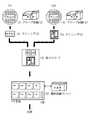
図1には、この発明に係る半導体装置の製造方法の一実施例を説明するための概略工程図が示されている。工程(1)では、半導体ウェハ上に複数のCPUチップを形成する。このようにCPUチップが半導体ウェハ上に形成された時点で、テスタによりプロービング試験(1)が行われる。上記CPUチップは、後述するようなメモリ回路及び自己診断等に用いられるユーザーデバッグ用インターフェイス回路を有している。 FIG. 1 is a schematic process diagram for explaining one embodiment of a method for manufacturing a semiconductor device according to the present invention. In step (1), a plurality of CPU chips are formed on a semiconductor wafer. When the CPU chip is thus formed on the semiconductor wafer, the probing test (1) is performed by the tester. The CPU chip has a memory circuit as will be described later and a user debug interface circuit used for self-diagnosis.
工程(2)では、前記同様に半導体ウェハ上に複数のメモリチップを形成する。このメモリチップは、例えばDDR−SDRAMのような大記憶容量で高速動作を行うものとされる。このようにメモリチップが半導体ウェハ上に形成された時点で、テスタによりプロービング試験(2)が行われる。 In step (2), a plurality of memory chips are formed on the semiconductor wafer in the same manner as described above. This memory chip is assumed to perform high-speed operation with a large storage capacity such as DDR-SDRAM. When the memory chip is thus formed on the semiconductor wafer, the probing test (2) is performed by the tester.
工程(3)では、上記CPUチップが形成された半導体ウェハのダンシング(1)が行われ、上記プローブ試験(1)で良品とされたCPUチップが選別される。 In step (3), the semiconductor wafer on which the CPU chip is formed is danced (1), and the CPU chips determined as good in the probe test (1) are selected.
工程(4)では、上記メモリチップが形成された半導体ウェハのダンシング(2)が行われ、上記プローブ試験(1)で良品とされたメモリチップが選別される。 In step (4), the semiconductor wafer on which the memory chip is formed is danced (2), and the memory chips determined as good in the probe test (1) are selected.
工程(5)では、上記工程(3)で良品とされたCPUチップと上記工程(4)で良品とされたメモリチップとが1つの搭載基板に搭載され、上記搭載基板に形成された内部配線により相互に接続されるとともに外部端子に接続される。そして、1つのモールド等によりチップ等が樹脂封止されて外観上1つの半導体装置として組み立てられる。 In the step (5), the CPU chip made good in the step (3) and the memory chip made good in the step (4) are mounted on one mounting substrate, and the internal wiring formed on the mounting substrate Are connected to each other and to an external terminal. Then, a chip or the like is resin-sealed by one mold or the like, and is assembled as one semiconductor device in appearance.
工程(6)では、上記組み立てられたSiPの選別試験が行われる。必要に応じてバーインも同時に行われる。この選別試験で用いられるテスト基板には、クロック生成回路CKGが搭載されており、テスト用ソケットに装着された被テストデバイスである上記SiP構成の半導体装置(PKG)に、実動作に相当する高速クロック信号を供給する。テスタは、上記テスト基板に搭載された複数の被テストデバイスPKGに対して、上記ユーザーデバッグ用インターフェイス回路を通してCPUチップをアクセスして、内蔵するメモリ回路に上記メモリチップの試験プログラムを書き込む。この後、上記CPUチップを起動して、上記内蔵メモリに格納されてプログラムに従ってメモリチップをアクセスして良否/判定結果を得て、それをテスタに転送する。CPUチップ自身の試験も、上記ユーザーデバッグ用インターフェイス回路を通してICE(インサーキットエミュレータ)モジュールをアクセスし、CPU及び上記内蔵メモリ回路を含んだ周辺回路のテストが行われる。このテスト結果からCPUチップ及びメモリチップが良品とされたSiPを出荷する。In step (6), a screening test of the assembled SiP is performed. Burn-in is also performed as needed. A clock generation circuit CKG is mounted on a test board used in the screening test, and the above-described SiP-structured semiconductor device (PKG), which is a device under test mounted in a test socket, has a high speed corresponding to an actual operation. Supply a clock signal. The tester accesses the CPU chip through the user debugging interface circuit to the plurality of devices under test PKG mounted on the test board, and writes the test program for the memory chip in the built-in memory circuit. Thereafter, the CPU chip is activated, and the memory chip is accessed according to a program stored in the built-in memory to obtain a pass / fail result, and the result is transferred to a tester. Test of the CPU chip itself, to access the ICE (in-circuit emulator) module viathe upper SL user debug interface circuit, testing of the peripheral circuits including the CPU and the internal memory circuit is performed. From this test result, the SiP in which the CPU chip and the memory chip are good products is shipped.
この実施例の選別試験では、上記SiPが実際に動作する状態と全く同じに、CPUチップがメモリチップを上記クロック信号に対応してメモリセルへの書き込み/読み出しを繰り返してメモリ試験を行うものである。この試験のためのプログラムの入力は、上記のようにテスタからテスト基板上に搭載された複数のSiPに同時に行われ、しかも、上記テスト基板上に搭載された複数のSiPでは、それぞれの入力されたプログラムに従って同時並行的にメモリチップの試験を行うので、上記のようなメモリ回路が大記憶容量を有するものであっても短時間にしかも一斉に終了させることができる。 In the screening test of this embodiment, the CPU chip performs the memory test by repeating writing / reading to / from the memory cell in response to the clock signal in exactly the same manner as the SiP actually operates. is there. The input of the program for this test is simultaneously performed from the tester to the plurality of SiPs mounted on the test board as described above, and each of the plurality of SiPs mounted on the test board is input respectively. Since the memory chips are tested in parallel according to the program, even if the memory circuit as described above has a large storage capacity, it can be completed in a short time all at once.
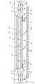
図2には、この発明に係るSiPの一実施例の説明図が示されている。図2(A)には、概略断面が示されて、図2(B)には上面が示されている。搭載基板1上に前記のようなマイクロコンピュータチップ2と、前記DDR−SDRAMチップ3とが搭載されている。搭載基板1の表面側には、マイクロコンピュータチップ2と、DDR−SDRAMが搭載され、それぞれがボンディングワイヤ4によって搭載基板の上面に設けられた配線パターンと接続される。上記マイクロコンピュータチップ2とDDR−SDRAMチップ3とは、いわゆるベアチップから構成されて搭載基板上にダイボンディングされる。 FIG. 2 shows an explanatory view of one embodiment of the SiP according to the present invention. 2A shows a schematic cross section, and FIG. 2B shows an upper surface. The
上記マイクロコンピュータチップ2は、搭載基板1に面付け可能な複数のバンプ電極を持つようにされてもよい。例えば、必要に応じてエリア・アレイ・パッドと称されるような技術、すなわち、素子及び配線が完成された半導体チップの回路形成面上にポリイミド樹脂からなるような絶縁膜を介してパッド電極(ボンディングパッド)の再配置を可能とする配線を形成し、かかる配線にパッド電極(バンプ接続用ランド電極)を形成するような技術によって構成されてもよい。上記エリア・アレイ・パッド技術によって、マイクロコンピュータチップ2における外部端子としての数十μmないし100μmピッチのような比較的小さいピッチに配列されたパッド電極は、0.1mm〜0.2mmのような径とされ、かつ400μm〜600μmピッチのような比較的大きなピッチのパンプ電極配列に変換される。 The
上記搭載基板1は、ガラスエポキシもしくはガラスからなるような絶縁基板と、かかる絶縁基板上に形成された多層配線構成からなるような比較的微細な内部配線と、上記ワイヤボンディグされるための電極が形成される。上記搭載基板1のマイクロコンピュータチップ2及びDDR−SDRAMチップが搭載される主面側は、ボンディングワイヤ4を含んで封止体5により封止されている。上記搭載基板1の裏面側には、外部端子としてのハンダボール6が設けられる。 The mounting
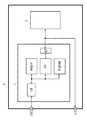
図3には、この発明に係るSiPの一実施例の内部ブロック図が示されている。同図においては、前記選別試験に関連する部分を中心にして示されている。この実施例の半導体装置(SiP)1は、マイクロコンピュータチップ2と、メモリチップ3から構成される。マイクロコンピュータチップ2は、CPU(中央処理装置)の他に、ICE(インサーキットエミュレータ:自己診断回路)モジュールを内蔵している。このICEモジュールは、特に制限されないが、JTAG準拠のインターフェイス回路を有し、外部端子JTAGに接続される。また、上記マイクロコンピュータチップ2には、スタティック型RAMのような内蔵メモリ及び周辺回路の他に、前メモリチップ3に対応したメモリインターフェイス回路IMFが設けられ、このメモリインターフェイス回路MIFを通して上記メモリチップ3と直接接続される。 FIG. 3 shows an internal block diagram of an embodiment of the SiP according to the present invention. In the figure, the portion related to the screening test is mainly shown. A semiconductor device (SiP) 1 according to this embodiment includes a
上記メモリチップ3は、特に制限されないが、高速で大記憶容量のDDR−SDRAMで構成される。入出力端子I/Oは、メモリチップ3を単独でテストするために設けられた外部端子である。この外部端子I/Oは、前記のように本願発明に係る選別試験そのものには必要としないが、例えばメモリチップをアクセスして選別試験前のバーインを効率良く行うための入力端子として用いることはできる。 The
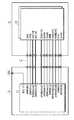
図4には、この発明に係るSiPの一実施例の内部ブロック図が示されている。同図においては、マイクロコンピュータチップ2とメモリチップ3との接続関係を中心にして示されている。メモリチップ3は、DDR−SDRAMである。端子CKEは、クロック・イネーブル入力である。端子CSBは、チップセレクト入力である。端子BA[1:0]は、バンクアドレス入力である。端子A[11:0]は、アドレス入力である。端子DQ[31:0]は、データ入出力である。端子RASBは、ロウ・アドレス・ストローブ入力である。端子CASBは、カラム・アドレス・ストローブ入力である。端子WEBは、ライト・イネーブル入力である。端子DQS[3:0]は、データ・ストローブ・入出力である。DQM[3:0]は、DQライト・マスク・イネーブル入力である。端子CLKとCLKBは、クロック入力である。 FIG. 4 shows an internal block diagram of an embodiment of the SiP according to the present invention. In the figure, the connection relationship between the
マイクロコンピュータチップ2においては、上記のようなDDR−SDRAMの入力端子、入出力端子にそれぞれ直接接続される各出力端子DDRCKE、DDRCS_N、DDRBA[1:0]、DDRA[11:0]、DDRRAS_N、DDRCAS_N、DDRWE_N、DDRRDM[3:0]、DDRCK,DDRCK_Nを有し、各入出力端子DDRD[31:0]、DDRDQS[3:0]を有している。同図において、メモリチップ3において、CSBのように端子名の最後にBを付したものは、ロウレベルをアクティブレベルとするバー信号であることを表している。これに対応して、マイクロコンピュータチップ2において、DDRCS_Nのように_Nを付したものは、ロウレベルがアクティブレベルであるネガティブ信号であることを示している。 In the
この実施例では、SiPのような半導体装置1において、上記マイクロコンピュータチップ2とメモリチップ3との間を接続する配線に接続されるテスト用端子が設けられる。このテスト用端子を用いることにより、例えばメモリチップに対して直接にアクセスすることができる。マイクロコンピュータチップ2は、マイクロコンピュータチップ2のユーザーデバッグ用インターフェイス回路に接続される端子JTAGが設けられる。 In this embodiment, in the
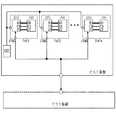
図5には、図4に示した半導体装置の選別試験を説明するための一実施例のブロック図が示されている。テスト基板には、クロック生成回路CKGが設けられており、被テストデバイスであるSiP1〜SiPnの実動作に対応したクロック信号が供給される。テスト基板上において、被テストデバイスSiP1〜SiPnは、前記テスト用端子(アドレスAD、コントロールCN端子及びデータ端子DT)が前記テスト装置とは接続されず、JTAG端子が共通にテスト装置と接続される。 FIG. 5 is a block diagram of an embodiment for explaining a screening test of the semiconductor device shown in FIG. A clock generation circuit CKG is provided on the test board, and a clock signal corresponding to the actual operation of SiP1 to SiPn that is a device under test is supplied. On the test substrate, the devices under test SiP1 to SiPn have the test terminals (address AD, control CN terminal and data terminal DT) not connected to the test apparatus, and the JTAG terminal is connected to the test apparatus in common. .
特に制限されないが、バーンインを行うときには、実際の動作電圧よりも高い動作電圧を供給し、高温雰囲気中でテスト用端子アドレスAD、コントロールCN端子及びデータ端子DTを用いて、上記テスト装置から実動作に比べて低い周波数によりメモリアクセスすることにより、初期不良の洗い出しを行うようにしてもよい。また、上記テスト用端子は、メモリチップ3とCPUチップ2との間の接続を確認する直流的な試験を行う上で便利である。Although not particularly limited, when burn-in is performed, an operating voltage higher than the actual operating voltage is supplied, and an actual operation is performed from the test apparatus using the test terminal address AD, the control CN terminal, and the data terminal DT in a high temperature atmosphere. The initial failure may be identified by accessing the memory at a lower frequency than the above. The test terminals are convenient for performing a DC test for confirming the connection between the
図6には、この発明に係るSiPの他の一実施例の内部ブロック図が示されている。同図においては、マイクロコンピュータチップ2とメモリチップ3との接続関係を中心にして示されている。この実施例では、前記図4のようにメモリチップ3に接続されるテスト用端子が省略される。つまり、メモリチップ3の端子CKE、端子CSB、端子BA[1:0]、端子A[11:0]、DQ[31:0]、端子RASB、端子CASB、端子WEB、端子DQS[3:0]、DQM[3:0]、及びCLKとCLKBは、マイクロコンピュータチップ2の各端子DDRCKE、DDRCS_N、DDRBA[1:0]、DDRA[11:0]、DDRD[31:0]、DDRRAS_N、DDRCAS_N、DDRWE_N、DDRDQS[3:0]、DDRRDM[3:0]、DDRCK,DDRCK_Nとそれぞれ相互に接続されるのみである。 FIG. 6 shows an internal block diagram of another embodiment of the SiP according to the present invention. In the figure, the connection relationship between the
図7には、前記図6に示した半導体装置の選別試験を説明するための一実施例のブロック図が示されている。テスト基板には、前記同様にクロック生成回路CKGが設けられており、被テストデバイスであるSiP1〜SiPnの実動作に対応したクロック信号が供給される。テスト基板上において、被テストデバイスSiP1〜SiPnは、JTAG端子が共通にテスト装置と接続される。 FIG. 7 is a block diagram showing an embodiment for explaining a screening test of the semiconductor device shown in FIG. A clock generation circuit CKG is provided on the test board in the same manner as described above, and a clock signal corresponding to the actual operation of SiP1 to SiPn as devices under test is supplied. On the test substrate, the devices under test SiP1 to SiPn have a JTAG terminal connected to a test apparatus in common.
この実施例では、前記のようにメモリチップ3の選別試験が、上記JTAGを用いて行い、メモリチップ3にはメモリテスト用端子が不要であるので省略される。上記JTAGを用いたマイクロコンピュータチップ2によるメモリチップ3の選別試験工程を含むSiPの製造方法を採用することにより、それにより製造されるSiPにおいては、例えば外部端子を約60本も大幅に削減することができる。このような外部端子の削減により、半導体装置(SiP)1においては、パッケージの小型化が可能になる。また、マイクロコンピュータチップ2とメモリチップ3との間を接続する配線と交差するメモリ用端子に向かう配線が不要となるので、その分の配線層を減らすことができる。したがって、SiPの搭載基板として、配線層の少ない安価なものを用いることもできるし、上記マイクロコンピュータチップ2とメモリチップ3との間の寄生容量も大幅に低減することができる。このような寄生容量の低減は、それをチャージ/ディスチャージするマイクロコンピュータチップ2、メモリチップ3の出力回路での電流が小さくて済むので動作の高速化や低消費電力化を図ることができる。 In this embodiment, as described above, the selection test of the
前記マイクロコンピュータチップ2は、本願出願人から販売されているSHシリーズのマイクロコンピュータチップのように、HUDI(ハイパフォーマンスユーザーデバッグインターフェイス)と呼ばれているようなユーザーデバッグ用インターフェイス回路を有している。このHUDIは、JTAG準拠の少数ピンで内部メモリを含むレジスタの読み書きができるものである。このようなユーザーデバッグ用インターフェイス回路を利用して、マイクロコンピュータチップ2の内部メモリに、上記メモリチップ3のメモリテストプログラムを格納させ、かかるメモリテストプログラムをマイクロコンピュータチップ2のCPUが実行することで、メモリチップの選別試験が行われる。もちろん、ユーザーデバッグ用インターフェイス回路は、本来の機能であるマイクロコンピュータチップ2の内部試験を行うために用いられる。 The
上記マイクロコンピュータチップ2の内部メモリへのメモリテストプログラムを書き込み、実行する手順の概略は、以下の通りである。
(1)CPUを「リセットホールド」状態にする。
(2)ASERAMにデータを書き込む。
(3)「HUDIブート」を実行する。
(4)内部RAMにメモリテストプログラム書き込む。
(5)メモリテストプログラムが正常に書き込まれた事を確認する。
(6)メモリテストプログラムを起動する。
(7)メモリテスト終了を待って結果を確認する。The outline of the procedure for writing and executing the memory test program in the internal memory of the
(1) The CPU is set to the “reset hold” state.
(2) Write data to ASERAM.
(3) Execute “HUDI boot”.
(4) Write a memory test program to the internal RAM.
(5) Confirm that the memory test program has been written normally.
(6) Start the memory test program.
(7) Wait for the end of the memory test and check the result.
メモリテストプログラムを実行するには、メモリテストプログラムをマイクロコンピュータチップ2の内部メモリに書込んでおく必要がある。メモリテストプログラムの容量を考慮し、メモリテストプログラムは、マイクロコンピュータチップ2の内部RAM(例えば、スタティック型ランダム・アクセス・メモリ)に書き込むようにする。例えば、前記SHマイクロコンピュータチップにおいては、前記HUDIを使った内部RAMヘの書き込みには「HUDI書込み命令」または「ASERAM書込み命令」がある。 In order to execute the memory test program, it is necessary to write the memory test program into the internal memory of the
「ASERAM書込み命令」はASERAM専用の書き込み命令である。内部RAMへの書き込みには「HUDI書込み命令」を使うことができるが、この命令はCPUが動作している状態でないと使えない。CPUを動作状態にするには、CPUをリセットしてスタートすればよいが、何の準備もなくリセットしたのでは、CPUが実行するプログラムが不確定であり、どのように動作するのかわからない。メモリテストプログラム書込み中にCPUがハングアップするかもしれないし、書き込んだデータを書き換えられるかもしれない。単にCPUをリセットしてスタートさせ、「HUDI書込み命令」で書き込み、「HUDI読出し命令」で書かれたデータを確認すると、書き込んだデータを読み出せない事が予測される。そこで、この実施例では、「リセットホールド」と「HUDIブート」を利用する。「リセットホールド」はCPUがリセット状態であるのに、ASERAMにプログラムが書きこめる状態であり、「HUDIブート」はASERAMに書き込んだプログラムを実行する手段である。「ASERAM書込み命令」でASERAMにプログラムを書き込み、これを実行中に内部RAMにメモリテストプログラムを書き込むことにする。「リセットホールド」状態で読み出して書き込んだデータを確認することもできる。 The “ASERAM write command” is a write command dedicated to ASERAM. A “HUDI write command” can be used for writing to the internal RAM, but this command can only be used when the CPU is operating. In order to put the CPU into an operating state, the CPU may be reset and started. However, if the CPU is reset without any preparation, the program executed by the CPU is indeterminate and it is not known how it operates. The CPU may hang up while writing the memory test program, and the written data may be rewritten. If the CPU is simply reset and started, data is written with a “HUDI write command”, and data written with a “HUDI read command” is confirmed, it is predicted that the written data cannot be read. Therefore, in this embodiment, “reset hold” and “HUDI boot” are used. “Reset hold” is a state in which a program can be written in ASERAM even though the CPU is in a reset state, and “HUDI boot” is a means for executing the program written in ASERAM. A program is written to the ASERAM by the “ASERAM write command”, and a memory test program is written to the internal RAM during execution of the program. The data read and written in the “reset hold” state can also be confirmed.
図8には、この発明に用いられるJTAG TAP(テスト・アクセス・ポート)の状態遷移図が示されている。同図において矢印横の‘0' または‘1' はTMS(テストモード)端子又は信号が‘0' または‘1' の時に状態が遷移することを示している。一般的にTAP制御遷移図の説明は抽象的でわかりずらいが、命令レジスタ(以下IR)に命令を書き込み、データレジスタ(以下DR)の読み書きをするだけである。命令コ−ドも、読み書きするデータも複数ビットあるので、1本のTDI(テストデータイン)端子からシフトステートでシリアルにデータを入力するだけのことである。 FIG. 8 shows a state transition diagram of a JTAG TAP (test access port) used in the present invention. In the figure, '0' or '1' next to the arrow indicates that the state transitions when the TMS (test mode) terminal or signal is '0' or '1'. Generally, the description of the TAP control transition diagram is abstract and difficult to understand, but only writes an instruction to an instruction register (hereinafter referred to as IR) and reads and writes data register (hereinafter referred to as DR). Since the instruction code and the data to be read and written are a plurality of bits, it is only necessary to input data serially in a shift state from one TDI (test data in) terminal.
ステート(1)(Test-Logic-Reset)は、HUDIリセットであり、TMS信号をハイレベルにしてTCK(テストクロック)信号を5回発生させることでこのステート(HUDIリセット)になる。
ステート(2)(Run-Test/Idle)は、通過点である。特定の命令が存在するときにのみICないのテストロジックがアクティブになる。例えば命令によりセルフテストをアクティブにした場合、このステートになったときにこの命令が実行される。それ以外のときは、テストロジックはアイドル状態となる。
ステート(3)(Select-DR ‐Scan) は、DRの読み書きであり、図下側(TMS=0)で実行、右側(TMS=1)で非実行である。
ステート(8)(Select-IR ‐Scan) は、IRの読み書きであり、図下側(TMS=0)で実行、下側(TMS=1)で非実行であり、上記ステート(1)に戻る。
ステート(4)(Capture-DR) は、読み出しデータの取り込みである。
ステート(9)(Capture-IR)は、読み出しデータの取り込みである。
ステート(5)(Shift-DR)は、読み出し、書き込みデータセットである。
ステート(10)(Shift-IR)は、読み出し、書き込みデータセットである。
ステート(6)(Exit-DR) は、単なる通過点である。
ステート(11)(Exit-IR) は、単なる通過点である。
ステート(7)(Update-DR)は、セットしたデータの書き込みである。
ステート(12)(Update-IR)は、セットしたデータの書き込みである。State (1) (Test-Logic-Reset) is a HUDI reset, and this state (HUDI reset) is obtained by setting the TMS signal to a high level and generating a TCK (test clock) signal five times.
State (2) (Run-Test / Idle) is a passing point. Only when a specific instruction is present, the test logic without IC is activated. For example, when the self test is activated by an instruction, the instruction is executed when the state is entered. At other times, the test logic is idle.
State (3) (Select-DR-Scan) is DR reading / writing, which is executed on the lower side (TMS = 0) and not executed on the right side (TMS = 1).
State (8) (Select-IR-Scan) is IR read / write, executed on the lower side (TMS = 0), not executed on the lower side (TMS = 1), and returns to the state (1). .
State (4) (Capture-DR) is fetching of read data.
State (9) (Capture-IR) is reading data reading.
State (5) (Shift-DR) is a read / write data set.
State (10) (Shift-IR) is a read / write data set.
State (6) (Exit-DR) is just a passing point.
State (11) (Exit-IR) is just a passing point.
State (7) (Update-DR) is writing of set data.
State (12) (Update-IR) is writing of set data.
図9には、この発明に用いられるJTAG TAP(テスト・アクセス・ポート)の一実施例の波形図が示されている。同図には、データレジスタを読み書きする例である。レジスタの読み書きは、必要な長さで打ち切ることができるので、この例では8ビットとしている。まず、TMS信号をTCKの5回分ハイレベル(‘1' )にしてTAPをリセット(状態R)する。その後TMS信号をTCKの立ち上がりエッジに時に‘0' −‘1' −‘0' にして前記ステート(2)(Run-Test/Idle)−ステート(3)(Select-DR ‐Scan) −ステート(4)(Capture-DR) のように遷移させる。状態は、I−S−Cのように略して示している。上記ステート(4)(Capture-DR) でデータを取り込み、次のステート(5)(Shift-DR) で取り込んだデータをTDO(テストデータアウト)端子から出力しながら、書き込むデータをセットする。ステート(5)(Shift-DR) は、S0〜S7の8サイクルからなり、TDIからDi0〜Di7のデータがシリアルに入力され、TDOからDo0〜Do7が出力される。このステート(5)(Shift-DR) の8サイクル目(S7)の後、TMS信号を‘1' −‘1' −‘0' に変化させてステート(6)(Exit-DR)−ステート(7)(Update-DR)−ステート(2)(Run-Test/Idle)と遷移させる。状態は、E−U−Iのように略して示している。このように1回のスキャンが終わったときはステート(2)(Run-Test/Idle)に戻しておくとわかりやすい。セットしたデータはステート(7)(Update-DR)で更新される。 FIG. 9 shows a waveform diagram of an embodiment of a JTAG TAP (Test Access Port) used in the present invention. The figure shows an example of reading and writing data registers. Since the reading and writing of the register can be terminated at the required length, this example uses 8 bits. First, the TMS signal is set to the high level ('1') for five times of TCK to reset the TAP (state R). Thereafter, the TMS signal is changed to “0”-“1”-“0” at the rising edge of TCK, and the state (2) (Run-Test / Idle) -state (3) (Select-DR-Scan) -state ( 4) Transition as shown in (Capture-DR). The state is abbreviated as I-S-C. Data is captured in the state (4) (Capture-DR), and the data to be written is set while outputting the data captured in the next state (5) (Shift-DR) from the TDO (test data out) terminal. State (5) (Shift-DR) consists of 8 cycles of S0 to S7, and data of Di0 to Di7 is input serially from TDI, and Do0 to Do7 are output from TDO. After the eighth cycle (S7) of state (5) (Shift-DR), the TMS signal is changed to '1'-'1'-'0' to change state (6) (Exit-DR) -state ( 7) Transition to (Update-DR) -state (2) (Run-Test / Idle). The state is abbreviated as EU. Thus, when one scan is completed, it is easy to understand by returning to the state (2) (Run-Test / Idle). The set data is updated in state (7) (Update-DR).
前記「リセットホールド」とは、CPUがリセット状態にあるにもかかわらず「ASERAM書き込み命令」を使って、ASERAMへ書き込みができる状態である。遷移方法は、端子又は信号/RESET及び/TRSTをロウレベルにする。製品チップモードとEVAチップモードを切り替えるピンがあるときには、HUDI機能を使用するときにはEVAチップモードにしておく。上記のように端子/RESET及び/TRSTを一定期間ロウレベルにすることでリセットホールド状態にすることができる。このリセット期間はある程度の時間が必要である。 The “reset hold” is a state in which writing to the ASERAM can be performed using an “ASERAM write command” even though the CPU is in a reset state. In the transition method, the terminal or signals / RESET and / TRST are set to low level. When there is a pin for switching between the product chip mode and the EVA chip mode, the EVA chip mode is set when the HUDI function is used. As described above, the terminals / RESET and / TRST are set to a low level for a certain period to set the reset hold state. This reset period requires a certain amount of time.
図10には、HUDIブートを説明するための波形図が示されている。HUDIブ−トを実行するためには、リセットホールド状態のときに 「HUDIブート命令」をIRにセットするだけである。IRは16ビットのレジスタであるが、下位ビットは何でも良い(don't care) ので上位8ビツトのみをセットする。前記図9と同様に状態R(Test-Logic-Reset)−I(Run-Test/Idle)−SD(Select-DR ‐Scan)−SI(Select-IR ‐Scan) −C(Capture-IR) のように遷移を行って前記ステート(10)(Shift-IR) を実行するとTDO(テストデータアウト)端子からは常に固定値が出力されている。このTDO端子を観測ればIRパスを実行していることが解る。「HUDIブート命令」が実行されると、「ASEブレークモード」となり、ASERAMの先頭番地に書かれているアドレスから実行が開始される。この時、ASEブレークフラグがセットされるので、「HUDI読出し命令」を使ってフラグをみることで、ASEブレークモードになっていることを確認できる。 FIG. 10 shows a waveform diagram for explaining the HUDI boot. To execute the HUDI boot, simply set the “HUDI boot instruction” to IR in the reset hold state. IR is a 16-bit register, but since the lower bits can be anything (don't care), only the upper 8 bits are set. Similarly to FIG. 9, the state R (Test-Logic-Reset) -I (Run-Test / Idle) -SD (Select-DR-Scan) -SI (Select-IR-Scan) -C (Capture-IR) Thus, when the state (10) (Shift-IR) is executed by making the transition as described above, a fixed value is always output from the TDO (test data out) terminal. If this TDO terminal is observed, it is understood that the IR path is being executed. When the “HUDI boot instruction” is executed, the “ASE break mode” is entered, and execution is started from the address written at the start address of ASERAM. At this time, since the ASE break flag is set, it can be confirmed that the ASE break mode is set by looking at the flag using the “HUDI read instruction”.
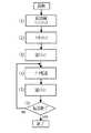
図11には、ASERAM書き込みモードの一実施例のフローチャート図が示されている。最初に、ステップ(1)ではSI(Select-IR ‐Scan)ステートにし、コマンドを書き込む。ステップ(2)では、書き込むアドレスをセットする。セットしたデ−タは開始アドレスと終了アドレスに配置される。例えば、上位16ビットで開始アドレスを下位16ビットで終了アドレスを指定する。アドレスの上位12ビットはASERAMが配置されるエリアに固定される。ステップ(3)〜(6)で、DRにデータをセットした後、転送フラグがセットされるまでSD(Select-DR ‐Scan)を繰り返す。 FIG. 11 shows a flowchart of an embodiment of the ASERAM write mode. First, in step (1), the SI (Select-IR-Scan) state is set and a command is written. In step (2), a write address is set. The set data is arranged at the start address and the end address. For example, the start address is designated by the upper 16 bits and the end address is designated by the lower 16 bits. The upper 12 bits of the address are fixed in the area where the ASERAM is placed. In steps (3) to (6), after data is set in DR, SD (Select-DR-Scan) is repeated until the transfer flag is set.
図12には、HUDI書込みモードの一実施例のフローチャート図が示されている。HUDI書込みには単独モードと連続モードがあり、それぞれに書き込みバイト数1、2,4バイトモードがある。同図には、連続モード書き込みの例が示されている。ステップ(1)ではSI(Select-IR ‐Scan) ステートにしてコマンドを書き込む。ステップ(2)では、書き込むアドレスをセットする。ステップ(3)〜(6)でHUDI書き込みでは初回は1回、2回目以降は2回目にフラグがセットされることを確認し、初回と2回目以降のDR‐Scanの数を変えている。 FIG. 12 shows a flowchart of one embodiment of the HUDI write mode. HUDI writing has a single mode and a continuous mode, and there are 1, 2, and 4 byte modes for the number of bytes to be written. In the figure, an example of continuous mode writing is shown. In step (1), the command is written in the SI (Select-IR-Scan) state. In step (2), a write address is set. In steps (3) to (6), it is confirmed that the flag is set once for the first time in HUDI writing, and the second time after the second time, and the number of DR-Scans for the first time and the second time or later is changed.
図13には、HDUI読出しモードの一実施例のフローチャート図が示されている。HUDI書込みと同様に単独モードと連続モードがあり、またそれぞれに書き込みバイト数1,2,4バイトモードがある。同図には、図12の書き込みと同じく連続モードのみである。ステップ(1)ではSI(Select-IR ‐Scan) ステートにしてコマンドを書き込む。読出しはテスト結果のように数バイト程度を想定しているため、読出し可能フラグを確認する。このため、ステップ(3)〜(6)で「HUDI読出し命令」を使用するときはDUT毎の個別読み出しとしている。 FIG. 13 shows a flowchart of an embodiment of the HDUI read mode. Similar to HUDI writing, there are a single mode and a continuous mode, and there are 1, 2, and 4 byte modes for the number of write bytes respectively. In the figure, only the continuous mode is used as in the writing in FIG. In step (1), the command is written in the SI (Select-IR-Scan) state. Since reading is assumed to be about several bytes like the test result, the readable flag is checked. For this reason, when the “HUDI read command” is used in steps (3) to (6), individual reading is performed for each DUT.
前記ICEモジュールによる外部メモリチップのテスト動作は次の(1)〜(6)通りである。(1)前記のようにCPUチップをリセットホールド状態にする。この状態にすることにより、CPUチップのICEモジュール内のRAM(ASERAM)にデータを書き込めるようになる。テスタは、この操作のためにJTAGで規定された前記端子とCPUチップの専用端子を制御する。 The test operation of the external memory chip by the ICE module is as follows (1) to (6). (1) The CPU chip is set to the reset hold state as described above. In this state, data can be written to the RAM (ASERAM) in the ICE module of the CPU chip. The tester controls the terminal defined by JTAG and the dedicated terminal of the CPU chip for this operation.
(2)ICEモジュール内の上記RAMにプログラムを書き込む。このプログラムは、テストプログラムの転送をサポートするためのものである。テスタは、書き込みのためにJTAGピンを使用する。(2) Write a program to the RAM in the ICE module. This program is for supporting the transfer of the test program. The tester uses the JTAG pin for writing.
(3)ICEモジュール内の上記RAMに書き込んだプログラムを実行する。テスタは、書き込みのためにJTAGピンを使用して専用のコマンドをCPUチップに送る。(3) The program written in the RAM in the ICE module is executed. The tester sends a dedicated command to the CPU chip using the JTAG pin for writing.
(4)内部RAMをアクセスしてメモリテストプログラムを書き込む。テスタは、書き込みのためにJTAGピンを使用する。(4) Access the internal RAM and write the memory test program. The tester uses the JTAG pin for writing.
(5)ICEモジュール内の上記RAMに書き込んだプログラムから上記メモリテストプログラムに分岐する。テスタは、書き込みのためにJTAGピンを使用する。(5) The program branches from the program written in the RAM in the ICE module to the memory test program. The tester uses the JTAG pin for writing.
(6)テスタは、テストの終了を監視し、テスト終了後に判定結果を読み取る。(6) The tester monitors the end of the test and reads the determination result after the end of the test.
前記PoPは、各搭載基板に半導体チップを実装した後に半導体装置同士を接続するので、半導体装置同士を接続する工程に先立って、半導体チップと搭載基板の接続状態を判定することが可能となり、パッケージの組み立て歩留まりの低減に有効である。さらに、SiPと比較してシステムの少量・多品種化にも柔軟に対応できる。しかしながら、前記図22に示したSiPと同様に、PoPのメモリ回路においても、図25に示されているようにアドレス端子AD、コントロール端子CN、データ端子DTに接続される試験用外部端子を設けて、テスト基板上に設けられたアドレスバス、コントロール信号及びデータバスに複数の被テストデバイスPoP1〜PoPnを接続して、テスト装置から直接に個々の被テストデバイスPoP1〜PoPnのメモリ回路のテストを行う場合には、高価な高速テスト装置が必要になるという問題を有するものである。 Since the PoP connects the semiconductor devices after mounting the semiconductor chips on each mounting substrate, it is possible to determine the connection state between the semiconductor chip and the mounting substrate prior to the step of connecting the semiconductor devices. This is effective in reducing the assembly yield. Furthermore, the system can be flexibly adapted to a small amount and a variety of systems as compared with SiP. However, similarly to the SiP shown in FIG. 22, the PoP memory circuit is also provided with a test external terminal connected to the address terminal AD, the control terminal CN, and the data terminal DT as shown in FIG. Then, by connecting a plurality of devices under test PoP1 to PoPn to the address bus, control signal and data bus provided on the test board, the memory circuits of the individual devices under test PoP1 to PoPn are directly tested from the test apparatus. In the case of performing it, there is a problem that an expensive high-speed test apparatus is required.
図14には、この発明に係る半導体装置の製造方法の他の一実施例を説明するための概略工程図が示されている。工程(1)では、半導体ウェハ上に複数のCPUチップを形成する。このようにCPUチップが半導体ウェハ上に形成された時点で、テスタによりプロービング試験(1)が行われる。上記CPUチップは、後述するようなメモリ回路及び自己診断等に用いられるユーザーデバッグ用インターフェイス回路を有している。 FIG. 14 is a schematic process diagram for explaining another embodiment of the semiconductor device manufacturing method according to the present invention. In step (1), a plurality of CPU chips are formed on a semiconductor wafer. When the CPU chip is thus formed on the semiconductor wafer, the probing test (1) is performed by the tester. The CPU chip has a memory circuit as will be described later and a user debug interface circuit used for self-diagnosis.
工程(2)では、前記同様に半導体ウェハ上に複数のメモリチップを形成する。このメモリチップは、例えばDDR−SDRAMのような大記憶容量で高速動作を行うものとされる。このようにメモリチップが半導体ウェハ上に形成された時点で、テスタによりプロービング試験(2)が行われる。 In step (2), a plurality of memory chips are formed on the semiconductor wafer in the same manner as described above. This memory chip is assumed to perform high-speed operation with a large storage capacity such as DDR-SDRAM. When the memory chip is thus formed on the semiconductor wafer, the probing test (2) is performed by the tester.
工程(3)では、上記CPUチップが形成された半導体ウェハのダンシング(1)が行われ、上記プローブ試験(1)で良品とされたCPUチップが選別される。 In step (3), the semiconductor wafer on which the CPU chip is formed is danced (1), and the CPU chips determined as good in the probe test (1) are selected.
工程(4)では、上記メモリチップが形成された半導体ウェハのダンシング(2)が行われ、上記プローブ試験(1)で良品とされたメモリチップが選別される。 In step (4), the semiconductor wafer on which the memory chip is formed is danced (2), and the memory chips determined as good in the probe test (1) are selected.
工程(5)では、上記工程(3)で良品とされたCPUチップが搭載基板に搭載される。搭載基板は、多層の配線層を有し表面(上面)にCPUチップが面実装され、その外側にメモリチップが搭載された半導体装置との接続を行う電極が形成される。 In step (5), the CPU chip determined as good in step (3) is mounted on the mounting substrate. The mounting substrate has a multilayer wiring layer, a CPU chip is surface-mounted on the surface (upper surface), and an electrode for connecting to a semiconductor device on which the memory chip is mounted is formed on the outer surface.
工程(6)では、上記工程(4)で良品とされたメモリチップが搭載基板に搭載される。このメモリチップは、その搭載基板の表面にフェイスアップ実装され、複数のAuワイヤを介して表面の信号用パッドに接続される。裏面側に上記CPUチップが搭載された搭載基板に形成された電極に対応したハンダボールが形成される。 In step (6), the memory chip determined as good in step (4) is mounted on the mounting substrate. This memory chip is mounted face-up on the surface of the mounting substrate, and is connected to a signal pad on the surface via a plurality of Au wires. Solder balls corresponding to the electrodes formed on the mounting substrate on which the CPU chip is mounted on the back side are formed.
工程(7)では、上記工程(5)で組み立てられたCPUチップが搭載された半導体装置の選別試験(1)が行われる。この選別試験(1)では必要に応じてバーンインも同時に行われる。 In step (7), a selection test (1) of the semiconductor device on which the CPU chip assembled in step (5) is mounted is performed. In the screening test (1), burn-in is also performed at the same time as necessary.
工程(8)では、上記工程(6)で組み立てられたメモリチップが搭載された半導体装置の選別試験(2)が行われる。この選別試験(2)では必要に応じてバーンインも同時に行われる。 In step (8), a selection test (2) of the semiconductor device on which the memory chip assembled in step (6) is mounted is performed. In this screening test (2), burn-in is also performed at the same time as necessary.
工程(9)では、上記工程(7)で良品とされたCPUチップが搭載された半導体装置の上部に、上記工程(8)で良品とされたメモリチップが搭載された半導体装置を重ね合わせて上記ハンダボールを介してCPUチップとメモリチップの対応する端子同士が接続された2層構造の積層型パッケージとして組み立てられる。 In step (9), the semiconductor device on which the memory chip determined to be non-defective in the step (8) is superimposed on the semiconductor device on which the CPU chip determined to be non-defective in the step (7) is mounted. A two-layer stacked package in which corresponding terminals of the CPU chip and the memory chip are connected via the solder balls is assembled.
工程(10)では、上記組み立てられたPoPの試験が行われる。この試験で用いられるテスト基板には、クロック生成回路CKGが搭載されており、テスト用ソケットに装着された被テストデバイスである上記半導体装置(PoP)に、実動作に相当する高速クロック信号を供給する。テスタは、上記テスト基板に搭載された複数の被テストデバイスPoPに対して、上記ユーザーデバッグ用インターフェイス回路を通してCPUチップをアクセスして、内蔵するメモリ回路に上記メモリチップの試験プログラムを書き込む。この後、上記CPUチップを起動して、上記内蔵メモリに格納されてプログラムに従ってメモリチップをアクセスして良否/判定結果を得て、それをテスタに転送する。CPUチップ自身の試験も、上記上記ユーザーデバッグ用インターフェイス回路を通してICE(インサーキットエミュレータ)モジュールをアクセスし、CPU及び上記内蔵メモリ回路を含んだ周辺回路のテストが行われる。 In step (10), the assembled PoP is tested. The test board used in this test is equipped with a clock generation circuit CKG and supplies a high-speed clock signal corresponding to the actual operation to the semiconductor device (PoP) which is a device under test mounted in the test socket. To do. The tester accesses the CPU chip through the user debugging interface circuit to the plurality of devices under test PoP mounted on the test board, and writes the test program for the memory chip in the built-in memory circuit. Thereafter, the CPU chip is activated, and the memory chip is accessed according to a program stored in the built-in memory to obtain a pass / fail result, and the result is transferred to a tester. In the test of the CPU chip itself, an ICE (in-circuit emulator) module is accessed through the user debug interface circuit, and a peripheral circuit including the CPU and the built-in memory circuit is tested.
上記工程(1)〜(10)は、1つの半導体メーカにより全て実施されるものの他、
特に制限されないが、上記工程(1),(3),(5),(7)は、CPUチップを形成する第1の半導体メーカで実施され、上記工程(2),(4),(6),(8)は、上記第1の半導体メーカとは異なるメモリチップを形成する第2の半導体メーカにて実施されてもよい。また、上記CPUチップを搭載した半導体装置を製造する各工程(1),(3),(5),(7)、上記メモリチップを搭載した半導体装置を製造する各工程(2),(4),(6),(8)は、適宜に複数のメーカが分担して行うようにするものであってもよい。上記工程(9)は、携帯電話装置等を形成するセットメーカにて実施されてもよい。この場合は、上記工程(10)の試験は、上記工程(9)と同じ上記セットメーカにて実施される。The above steps (1) to (10) are all implemented by one semiconductor manufacturer,
Although not particularly limited, the steps (1), (3), (5), and (7) are performed by the first semiconductor manufacturer that forms the CPU chip, and the steps (2), (4), and (6) are performed. ), (8) may be implemented by a second semiconductor manufacturer that forms a memory chip different from the first semiconductor manufacturer. Further, each step (1), (3), (5), (7) for manufacturing a semiconductor device mounted with the CPU chip, and each step (2), (4) for manufacturing a semiconductor device mounted with the memory chip. ), (6), and (8) may be performed by a plurality of manufacturers as appropriate. The step (9) may be performed by a set manufacturer that forms a mobile phone device or the like. In this case, the test in the step (10) is performed by the same set manufacturer as in the step (9).
この実施例の工程(10)の試験では、上記PoPが実際に動作する状態と全く同じに、CPUチップが搭載された半導体装置がメモリチップが搭載された半導体装置を上記クロック信号に対応してメモリセルへの書き込み/読み出しを繰り返してメモリ試験を行うものである。この試験のためのプログラムの入力は、上記のようにテスタからテスト基板上に搭載された複数のPoPに同時に行われ、しかも、上記テスト基板上に搭載された複数のPoPでは、それぞれの入力されたプログラムに従って同時並行的にメモリチップの試験を行うので、上記のようなメモリ回路が大記憶容量を有するものであっても短時間にしかも一斉に終了させることができる。 In the test of the step (10) of this embodiment, the semiconductor device on which the CPU chip is mounted corresponds to the clock signal in the same manner as the PoP actually operates. A memory test is performed by repeatedly writing to and reading from a memory cell. The input of the program for this test is simultaneously performed from the tester to the plurality of PoPs mounted on the test board as described above, and each of the plurality of PoPs mounted on the test board is input respectively. Since the memory chips are tested in parallel according to the program, even if the memory circuit as described above has a large storage capacity, it can be completed in a short time all at once.
CPUチップが搭載された半導体装置及びメモリチップが搭載された半導体装置は、それ自体がバーンインを含んだ選別試験(1)(2)が実施されるものであるが、それは単体の状態での試験であり、上記PoPとして組み立てられた状態での試験ではない。PoP構造の半導体装置では、2つの半導体装置が狭い間隔を持って積層的にスタックさせられているので、それぞれの発熱が互いに強く影響し合うと予測される。したがって、PoP構造の半導体装置として組み立てられた状態での実動作に対応したクロックでのメモリ試験を行うことは、上記PoP構造の半導体装置のCPU及びメモリの性能を共に保証するためにも是非とも必要になるものである。 The semiconductor device on which the CPU chip is mounted and the semiconductor device on which the memory chip is mounted are subjected to a screening test (1) (2) including burn-in itself. It is not a test in a state assembled as the PoP. In a semiconductor device having a PoP structure, since two semiconductor devices are stacked in a stacked manner with a narrow interval, it is predicted that each heat generation strongly influences each other. Therefore, performing a memory test with a clock corresponding to an actual operation in a state where the semiconductor device is assembled as a PoP structure semiconductor device is sure to guarantee both the performance of the CPU and the memory of the semiconductor device with the PoP structure. It is necessary.
図15には、この発明が適用されるPoP構造の半導体装置の一実施例の概略断面図が示されている。CPUチップ12が実装された第1の搭載基板13と、メモリチップ14が実装された第2の搭載基板15は、上記第2の搭載基板15の裏面に形成された複数のハンダボール22を介して、上記第1の搭載基板13の対応する電極に電気的に接続される。上記第1の搭載基板13の表面の中央部には上記CPUチップ12が実装されるので、これらのハンダボール22は、第2の搭載基板15の裏面の外周部に沿って配置される。第1の搭載基板13の表面の外周部(CPUチップ12の外側)には、これらのハンダボール22が接続される電極パッドが形成される。メモリチップ14は、特に制限されないが、DDR−SDRAMであり、Auワイヤ(ボンディングワイヤ)26により第2の搭載基板15のボンディングパッドと接続される。このボンディングパッドと上記第2の搭載基板15の裏面の電極パッドとは、基板表面の信号配線、それらを接続するビアホールを介して電気的に接続される。上記メモリチップ14、Auワイヤ26および電極パッドは、モールド樹脂30によって気密封止されている。 FIG. 15 is a schematic sectional view showing an embodiment of a semiconductor device having a PoP structure to which the present invention is applied. The first mounting
CPUチップ12は、その主面(下面)に形成された複数のハンダボール21を介して、搭載基板13の表面の電極パッドにフリップチップ接続(フェイスダウン接続)されている。CPUチップ12の主面は、アンダーフィル樹脂によって気密封止されている。上記第1の搭載基板13の裏面には、格子上に配列された複数の外部入出力信号用電極パッドが形成され、これらの電極パッド上にはハンダボール23が接続される。第1の搭載基板13の表面の信号用パッドと裏面の外部入出力信号用パッドは、基板表面の信号配線、内層の信号配線およびそれらを接続するビアホールを介して電気的に接続される。 The
図16には、この発明が適用されるPoP構造の半導体装置の他の一実施例の概略断面図が示されている。この実施例では、メモリチップが搭載された上側の半導体装置には、2つのメモリチップ14が搭載される。つまり、同じ記憶容量のDDR−SDRAMを2個搭載することにより、前記図15の2倍の記憶容量を実現するものである。2つのメモリチップ14は、スペーサとしてのダミーチップ25を介して積層される。このダミーチップ25により、下側のメモリチップ14に対するAuワイヤ26のスペースが確保される。他の構成は、前記図15と同様である。 FIG. 16 is a schematic sectional view showing another embodiment of a semiconductor device having a PoP structure to which the present invention is applied. In this embodiment, two
図17には、この発明が適用されるPoP構造の半導体装置の他の一実施例の概略断面図が示されている。この実施例では、メモリチップが搭載された上側の半導体装置には、3種類のメモリチップ14が積層されて搭載される。例えば、DDR−SDRAMと、SDRAM及び一括消去型不揮発メモリ(フラッシュメモリ)のような3種類のメモリチップからなる。この場合、サイズの大きなメモリチップが下側にされて、メモリチップに設けられるボンディングパッド及びAuワイヤのスペースが確保される。メモリチップのサイズがほぼ同じなら、前記図16のようにダミーチップを介在させて3種類のメモリチップを積層構造にすればよい。この場合には、下側のCPUチップ12において、上記3種類のメモリチップを直接接続することが可能なインターフェイス回路が設けられるものである。他の構成は、前記図15,図16と同様である。 FIG. 17 is a schematic sectional view showing another embodiment of a semiconductor device having a PoP structure to which the present invention is applied. In this embodiment, three types of
図18には、前記図16に対応した半導体装置の一実施例の断面図が示されている。この実施例のPoP構造の半導体装置は、CPUチップ12が実装された搭載基板(第1の配線基板)13の上部に、メモリチップ14が実装された搭載基板(第2配線基板)15を重ね合わせた2層構造の積層型パッケージである。上記CPUチップ12は、例えば前記同様に本願出願人から販売されているSHシリーズのマイクロコンピュータチップのように、HUDI(ハイパフォーマンスユーザーデバッグインターフェイス)と呼ばれているようなユーザーデバッグ用インターフェイス回路を有している。 FIG. 18 is a sectional view showing an embodiment of the semiconductor device corresponding to FIG. In the semiconductor device having the PoP structure of this embodiment, a mounting board (second wiring board) 15 on which a
このHUDIは、JTAG準拠の少数ピンで内部メモリを含むレジスタの読み書きができるものである。このようなユーザーデバッグ用インターフェイス回路を利用して、CPUチップ12の内部メモリに、上記メモリチップ14のメモリテストプログラムを格納させ、かかるメモリテストプログラムをCPUチップ12のCPUが実行することで、メモリチップ14の試験が行われる。もちろん、ユーザーデバッグ用インターフェイス回路は、本来の機能であるCPUチップ12の内部試験を行うために用いられる。上記CPUチップ12には、スタティック型RAMのような内蔵メモリ及び周辺回路の他に、前メモリチップ14に対応したメモリインターフェイス回路(DDR−SDRAM、SDRAM、一括消去型不揮発性メモリ)が設けられ、このメモリインターフェイス回路を通して上記対応するメモリチップ14と直接接続される。 This HUDI can read and write a register including an internal memory with a small number of pins compliant with JTAG. By using such a user debugging interface circuit, the memory test program of the
この実施例の半導体装置は、搭載基板15の表面(上面)に約512メガビットのDDR−SDRAMチップ14をダミーチップ25を介して2枚積層して約1ギガビットの記憶容量を実現している。上記搭載基板15に実装されるメモリチップ14の記憶容量や枚数は、適宜変更することができる。すなわち、PoP構造の半導体装置は、メモリ搭載基板15に実装するメモリチップ14の記憶容量や枚数を変更することにより、CPUチップ12が実装されたベースとしての搭載基板13側の仕様をほとんど変更することなく、多品種の半導体装置を製造することができる。 The semiconductor device of this embodiment realizes a storage capacity of about 1 gigabit by stacking two DDR-
搭載基板13は、例えばビルドアップ工法によって製造された6層の配線(表面配線、裏面配線および4層の内層配線)を有する多層配線基板であり、配線層同士を電気的に絶縁する絶縁層は、ガラス繊維または炭素繊維に樹脂を含浸させたプリプレグによって構成されている。6層の配線は、例えば銅(Cu)を主体とする導電膜によって構成されている。図18には、これらの配線の図示が省略されており、搭載基板13の表面(上面)に形成された電極パッド16p、17p、18pと、搭載基板13の裏面に形成された外部入出力用電極パッド19pのみが例示されている。 The mounting
CPUチップ12は、その主面(下面)に形成された複数のハンダボール21を介して、ベース基板13の表面の電極パッド16p、17pにフリップチップ接続(フェイスダウン接続)されている。CPUチップ12の主面は、アンダーフィル樹脂24によって気密封止されている。図示は省略するが、CPUチップ12は、入出力端子の数が極めて多いので、ボンディングパッド(およびその表面に接続されたハンダボール21)は、CPUチップ12の主面の4辺に沿って2列に配置され、かつ、内側の列のボンディングパッドと外側の列のボンディングパッドは、千鳥状に配置されている。 The
搭載基板13の裏面には、複数の外部入出力用電極パッド19pが形成されており、それらの表面にはハンダボール23が電気的に接続されている。PoP構造の半導体装置は、これらのハンダボール23を介して情報通信端末機器のマザーボードに実装される。図示は省略されているが、搭載基板13の表面の配線と裏面の外部入出力用電極パッド19pは、内層配線およびそれらを接続するビアホールを介して電気的に接続されている。 A plurality of external input /
2枚のメモリチップ14が実装されたメモリ搭載基板15は、ガラスエポキシ樹脂などを絶縁層とする樹脂基板からなる。2枚のメモリチップ14は、その一方がメモリ基板15の表面にフェイスアップ実装されており、もう一方がダミーチップ25を介して上記メモリチップ14の上に積層されている。2枚のメモリチップ14のそれぞれは、Auワイヤ26を介してメモリチップ14の表面の電極パッド27に電気的に接続されている。2枚のメモリチップ14、ダミーチップ25、Auワイヤ26および電極パッド27は、モールド樹脂30によって気密封止されている。メモリ搭載基板15の裏面には、図示しないビアホールを介して上記電極パッド27に電気的に接続された電極パッド28が形成されており、その表面にはハンダボール22が電気的に接続されている。電極パッド27、28のそれぞれは、例えばメモリ搭載基板15の対向する外周部に沿って2列に配置されている。 The
メモリ搭載基板15の電極パッド28に接続されたハンダボール22は、搭載基板13の表面の外周部に形成された電極パッド18pにも電気的に接続されており、これにより、CPUチップ12が実装された搭載基板13とメモリチップ14が実装されたメモリ搭載基板15とが電気的に接続されている。ハンダボール22は、搭載基板13に実装されたCPUチップ12の上面とメモリ搭載基板15の下面とが接触しないよう、CPUチップ12の主面に形成されたハンダボール21の直径とCPUチップ12の厚さとを合計した厚さよりも大きい直径を有している。前述したように、搭載基板13の裏面には、外部入出力用電極パッド19pが形成されている。外部入出力用電極パッド19pにはハンダボール23が接続される。 The
図19には、前記図18に示した半導体装置の一実施例の一部拡大断面図が示されている。図19に示す例では、CPUチップ12とメモリチップ14の対応する信号端子は、外側の列の電極パッド17pと一体に形成された表面配線31、ビアホール32および第2層配線33を介して電気的に接続されている。配線設計ルールの制約により、外側の列の電極パッド17pを介してCPUチップ12とメモリチップ14を電気的に接続することができない箇所が生じた場合は、内側の列の電極パッド16pを介してCPUチップ12とメモリチップ14を電気的に接続する。例えば、CPUチップ12とメモリチップ14とは、内側の列の電極パッド16pと、前記ビアホール32及び外側の列の電極パッド17pよりもさらに内側に延在する第2層配線を介して電気的に接続させればよい。 FIG. 19 is a partially enlarged sectional view of one embodiment of the semiconductor device shown in FIG. In the example shown in FIG. 19, the corresponding signal terminals of the
特に制限されないが、搭載基板13には、メモリチップ14に対して直接アクセスできるようにするテスト用電極パッドが設けられない。これにより、前記CPUチップ12とメモリチップ14との間に、テスト用電極パッド及びそれを接続させるための配線が不要となり、上記テスト用電極パッド及びそれを接続させるための配線を形成するのに必要な面積だけ搭載基板13のサイズを小さくできることの他、CPUチップ12とメモリチップ14との間の信号伝達での寄生容量の低減や信号の反射やカップリング等によるノイズ低減が図れてDDR−SDRAMのような高速メモリに適した信号伝達が可能になる。また、搭載基板13に形成される配線層の量が少なくなるので、配線層と絶縁層(プリプレグ)の熱膨張係数差に起因する搭載基板13の反りを抑制することができる。 Although not particularly limited, the mounting
図20には、この発明に係るPoPの一実施例の内部ブロック図が示されている。この実施例のPoPは、前記図16の半導体装置に対応している。同図においては、CPUチップ12とメモリチップ14との接続関係を中心にして示されている。メモリチップ14は、DDR−SDRAMである。端子CKEは、クロック・イネーブル入力である。端子CSBは、チップセレクト入力である。端子BA[1:0]は、バンクアドレス入力である。端子A[11:0]は、アドレス入力である。端子DQ[31:0]は、データ入出力である。端子RASBは、ロウ・アドレス・ストローブ入力である。端子CASBは、カラム・アドレス・ストローブ入力である。端子WEBは、ライト・イネーブル入力である。端子DQS[3:0]は、データ・ストローブ・入出力である。DQM[3:0]は、DQライト・マスク・イネーブル入力である。端子CLKとCLKBは、クロック入力である。 FIG. 20 shows an internal block diagram of an embodiment of PoP according to the present invention. The PoP in this embodiment corresponds to the semiconductor device of FIG. In the figure, the connection relationship between the
同図では、特に制限されないが、約512MビットのようなDDR−SDRAMが2個設けられることにより、全体で約1ギガビットの記憶容量を持つようにされる。上記2つのDDR−SDRAMは、端子DQ[31:0]がそれぞれCPUチップ12の対応する64ビットのデータ入出力端子に接続されることにより、64ビット単位での書き込み/読み出しが行うようにされる。あるいは、端子DQ[31:0]がCPUチップ12の対応する32ビットのデータ入出力端子に並列接続される。この場合には、例えば上記2つのDDR−SDRAMのチップセレクト端子CSBに、CPUチップ12から選択信号を供給し、2つのうちのいずれか1つのDDR−SDRAMが選択されるようにする。あるいは、アドレス端子に拡張アドレス信号を供給して2つのうちのいずれか1つのDDR−SDRAMを選択するようにしてもよい。 In the figure, although not particularly limited, by providing two DDR-SDRAMs of about 512 Mbits, the total storage capacity is about 1 gigabit. In the two DDR-SDRAMs, the terminals DQ [31: 0] are respectively connected to the corresponding 64-bit data input / output terminals of the
CPUチップ12においては、上記のようなDDR−SDRAMの入力端子、入出力端子にそれぞれ直接接続される各出力端子DDRCKE、DDRCS_N、DDRBA[1:0]、DDRA[11:0]、DDRRAS_N、DDRCAS_N、DDRWE_N、DDRRDM[3:0]、DDRCK,DDRCK_Nを有し、各入出力端子DDRD[31:0]、DDRDQS[3:0]を有している。同図において、メモリチップ14において、CSBのように端子名の最後にBを付したものは、ロウレベルをアクティブレベルとするバー信号であることを表している。これに対応して、CPUチップ12において、DDRCS_Nのように_Nを付したものは、ロウレベルがアクティブレベルであるネガティブ信号であることを示している。 In the
この実施例では、PoPのような半導体装置において、上記CPUチップ12とメモリチップ14との間を接続する信号経路にテスト用端子が設けられる。このテスト用端子を用いることにより、例えばメモリチップ14に対して直接にアクセスすることができる。CPUチップ12は、CPUチップ12のユーザーデバッグ用インターフェイス回路に接続される端子JTAGが設けられる。上記テスト用端子は、メモリチップ14とCPUチップ12との間のハンダボール22による接続を確認する直流的な試験を行う上で便利である。しかしながら、端子JTAGを用いて前記のようにPoP構造の半導体装置として組み立てられた状態での実動作に対応したクロックでのメモリ試験を行うことは、上記PoP構造の半導体装置のCPU及びメモリの性能を共に保証すること及び高価なテスト装置が不要にできるものである。 In this embodiment, in a semiconductor device such as PoP, a test terminal is provided in a signal path connecting the
図21には、この発明に係るPoPの他の一実施例の内部ブロック図が示されている。この実施例のPoPは、前記図16の半導体装置に対応している。同図においては、CPUチップ12とメモリチップ14との接続関係を中心にして示されている。この実施例では、前記図20のようにメモリチップ14に接続されるテスト用端子が省略される。つまり、メモリチップ14の端子CKE、端子CSB、端子BA[1:0]、端子A[11:0]、DQ[31:0]、端子RASB、端子CASB、端子WEB、端子DQS[3:0]、DQM[3:0]、及びCLKとCLKBは、CPUチップ12の各端子DDRCKE、DDRCS_N、DDRBA[1:0]、DDRA[11:0]、DDRD[31:0]、DDRRAS_N、DDRCAS_N、DDRWE_N、DDRDQS[3:0]、DDRRDM[3:0]、DDRCK,DDRCK_Nとそれぞれ相互に接続されるのみである。他の構成は、前記図20と同様である。 FIG. 21 shows an internal block diagram of another embodiment of the PoP according to the present invention. The PoP in this embodiment corresponds to the semiconductor device of FIG. In the figure, the connection relationship between the
図22には、前記図21に示した半導体装置の動作試験を説明するための一実施例のブロック図が示されている。テスト基板には、前記同様にクロック生成回路CKGが設けられており、被テストデバイスであるPoP1〜PoPnの実動作に対応したクロック信号が供給される。テスト基板上において、被テストデバイスPoP1〜PoPnは、JTAG端子が共通にテスト装置と接続される。 FIG. 22 is a block diagram showing one embodiment for explaining an operation test of the semiconductor device shown in FIG. A clock generation circuit CKG is provided on the test board in the same manner as described above, and a clock signal corresponding to the actual operation of PoP1 to PoPn that is a device under test is supplied. On the test board, the devices under test PoP1 to PoPn have JTAG terminals connected to the test apparatus in common.
この実施例では、前記のようにメモリチップ14の動作試験は、上記JTAGを用いて行われるので、メモリチップ14にはメモリテスト用端子が不要であるので省略できる。上記JTAGを用いたCPUチップ12によるメモリチップ14の動作試験工程を含むPoPの前記図14に示した製造方法を採用することにより、それにより製造されるPoPにおいては、例えば外部端子を約60本も大幅に削減することができる。このような外部端子の削減により、半導体装置(PoP)においては、パッケージの小型化が可能になる。つまり、前記図16に示した搭載基板13の裏面側に設けられるタスト用ハンダボール又はテスト用電極及びそれに接続させるための配線が不要となり、搭載基板13のサイズを小さくすることができる。 In this embodiment, since the operation test of the
また、前記図20のブロック図のように上記CPUチップ12とメモリチップ14との間を接続する配線と交差するメモリ用端子に向かう配線が不要となるので、その分の配線層を減らすことができる。したがって、PoPの搭載基板13として、配線層の少ない安価なものを用いることもできるし、配線層と絶縁層(プリプレグ)の熱膨張係数差に起因する搭載基板13の反りを抑制することができる。この反りの抑制により、搭載基板13と搭載基板15の間とを接続するハンダボール22に加わる機械的ストレスを低減し、高い信頼性での接続が可能になる。上記CPUチップ12とメモリチップ14との間の寄生容量も大幅に低減することができる。このような寄生容量の低減は、それをチャージ/ディスチャージするCPUチップ12、メモリチップ14の出力回路での電流が小さくて済むので動作の高速化や低消費電力化を図ることができる。 Further, as shown in the block diagram of FIG. 20, since the wiring toward the memory terminal intersecting with the wiring connecting the
前記CPUチップ12は、前記のように本願出願人から販売されているSHシリーズのマイクロコンピュータチップのように、HUDI(ハイパフォーマンスユーザーデバッグインターフェイス)と呼ばれているようなユーザーデバッグ用インターフェイス回路を有している。このHUDIは、JTAG準拠の少数ピンで内部メモリを含むレジスタの読み書きができるものである。このようなユーザーデバッグ用インターフェイス回路を利用して、CPUチップ12の内部メモリに、上記メモリチップ14のメモリテストプログラムを格納させ、かかるメモリテストプログラムをCPUチップ12のCPUが実行することで、メモリチップの動作試験が行われる。もちろん、ユーザーデバッグ用インターフェイス回路は、本来の機能であるマイクロコンピュータチップ2の内部試験を行うために用いられる。 The
上記CPUチップ12の内部メモリへのメモリテストプログラムを書き込み、実行する手順の概略は、前記SiPと同様に以下の通りである。
(1)CPUを「リセットホールド」状態にする。
(2)ASERAMにデータを書き込む。
(3)「HUDIブート」を実行する。
(4)内部RAMにメモリテストプログラム書き込む。
(5)メモリテストプログラムが正常に書き込まれた事を確認する。
(6)メモリテストプログラムを起動する。
(7)メモリテスト終了を待って結果を確認する。The outline of the procedure for writing and executing the memory test program to the internal memory of the
(1) The CPU is set to the “reset hold” state.
(2) Write data to ASERAM.
(3) Execute “HUDI boot”.
(4) Write a memory test program to the internal RAM.
(5) Confirm that the memory test program has been written normally.
(6) Start the memory test program.
(7) Wait for the end of the memory test and check the result.
メモリテストプログラムを実行するには、メモリテストプログラムをCPUチップ12の内部メモリに書込んでおく必要がある。メモリテストプログラムの容量を考慮し、メモリテストプログラムは、CPUチップ12の内部RAM(例えば、スタティック型ランダム・アクセス・メモリ)に書き込むようにする。例えば、前記SHマイクロコンピュータチップにおいては、前記同様にHUDIを使った内部RAMヘの書き込みには「HUDI書込み命令」または「ASERAM書込み命令」がある。 In order to execute the memory test program, it is necessary to write the memory test program into the internal memory of the
以上本発明者よりなされた発明を実施例に基づき具体的に説明したが、本願発明は前記実施例に限定されるものではなく、その要旨を逸脱しない範囲で種々変更可能であることはいうまでもない。例えば、マイクロコンピュータチップに設けられるICEモジュールの構成は、種々の実施形態を採ることができる。ICEモジュールを起動するインターフェイス回路は、JTAGの他に何であってもよい。メモリチップは、DDR−SDRAMの他にSDRAM、あるいはSRAMであってもよし、フラッシュメモリ(一括消去型不揮発性メモリ)のような他の種類のメモリチップが搭載されるものであってもよい。SiPは、前記図2のように搭載基板の表面部に各チップを搭載するもの他、複数のチップを積層構造に組み立てるものであってもよい。 The invention made by the inventor has been specifically described based on the embodiments. However, the invention of the present application is not limited to the embodiments, and various modifications can be made without departing from the scope of the invention. Nor. For example, the configuration of the ICE module provided in the microcomputer chip can take various embodiments. The interface circuit that activates the ICE module may be anything other than JTAG. The memory chip may be SDRAM or SRAM in addition to DDR-SDRAM, or may be mounted with other types of memory chips such as flash memory (batch erase nonvolatile memory). The SiP may be one in which each chip is mounted on the surface portion of the mounting substrate as shown in FIG.
この発明は、マイクロコンピュータチップ(CPUチップ)とメモリチップを含むようなSiP、PoP又はマルチチップ構成の半導体装置及びその製造方法とテスト方法に広く利用することができる。 The present invention can be widely used for SiP, PoP or multi-chip semiconductor devices including a microcomputer chip (CPU chip) and a memory chip, and methods for manufacturing and testing the same.
1…搭載基板、2…マイクロコンピュータチップ、3…メモリチップ(DDR−SDRAM)、4…ボンディグワイヤ、5…封止体、6…ハンダボール、
12…CPUチップ、13…ベースとなる搭載基板、14…メモリチップ、15…メモリ搭載基板、16p,17p,18p,19p…電極パッド、21,22,23…ハンダボール、24…アンダーフィル樹脂、25…ダミーチップ、26…Auワイヤ、27,28…電極パッド、30…モールド樹脂、31…表面配線、32…ビアホール、33…第2層配線、
CPU…中央処理装置(マイクロプロセッサ)、MIF…メモリインターフェイス回路、ICE…インサーキットエミュレータ、SiP1〜SiPn,POP1〜PoPn…半導体装置(被テストデバイス)、CKG…クロック生成回路、TST1〜TSTn…テスト回路、FSM…フラッシュメモリ。DESCRIPTION OF
DESCRIPTION OF
CPU ... Central processing unit (microprocessor), MIF ... Memory interface circuit, ICE ... In-circuit emulator, SiP1 to SiPn, POP1 to PoPn ... Semiconductor device (device under test), CKG ... Clock generation circuit, TST1 to TSTn ... Test circuit , FSM ... Flash memory.
Claims (28)
Translated fromJapanese上記第1半導体装置の電気的試験を行い良品を選別する第2工程と、
プログラムに従った信号処理を行う信号処理回路と第2メモリ回路を有する第2半導体装置を形成する第3工程と、
上記第2半導体装置の上記信号処理回路及び第2メモリ回路の電気的試験を行い良品を選別する第4工程と、
上記第2工程で選別された上記第1半導体装置と上記第4工程で選別された上記第2半導体装置とを一体的に構成し、それぞれの対応する端子同士を接続する第5工程と、
上記第5工程で一体的に構成された上記半導体装置を試験用基板に搭載して電気的に試験して上記半導体装置の良否判定する第6工程とを有し、
上記第6工程は、
上記試験用基板には、上記半導体装置の実動作に相当したクロック信号を上記複数の半導体装置に共通に供給する発振回路が設けられており、
テスト装置から上記第2半導体装置の第2メモリ回路に上記第1半導体装置の第1メモリ回路の動作試験を行うテストプログラムを書き込む第1動作と、
上記第2半導体装置の上記信号処理回路により、上記クロック信号に対応して上記第2メモリ回路に書き込まれたテストプログラムに従って上記第1半導体装置の第1メモリ回路の動作試験を行う第2動作と、
上記第2動作での良否判定結果を上記テスト装置に出力させる第3動作とを有し、上記第2メモリ回路は、スタティック型RAMである半導体装置の製造方法。A first step of forming a first semiconductor device having a first memory circuit;
A second step of performing an electrical test on the first semiconductor device to select non-defective products;
A third step of forming a second semiconductor device having a signal processing circuit for performing signal processing according to a program and a second memory circuit;
A fourth step of performing an electrical test on the signal processing circuit and the second memory circuit of the second semiconductor device to select non-defective products;
A fifth step of integrally configuring the first semiconductor device selected in the second step and the second semiconductor device selected in the fourth step, and connecting corresponding terminals;
And a sixth step of determining the quality of the semiconductor device by mounting the semiconductor device integrally configured in the fifth step on a test substrate and electrically testing it.
The sixth step is
The test substrate is provided with an oscillation circuit that supplies a clock signal corresponding to the actual operation of the semiconductor device to the plurality of semiconductor devices in common.
A first operation of writing a test program for performing an operation test of the first memory circuit of the first semiconductor device from a test device to the second memory circuit of the second semiconductor device;
A second operation for performing an operation test of the first memory circuit of the first semiconductor device by the signal processing circuit of the second semiconductor device according to a test program written in the second memory circuit corresponding to the clock signal; ,
The quality determination result of the second operationhave a third operation and to output to the testdevice,the second memory circuit, a method of manufacturing a semiconductor device is astatic type RAM.
上記第1工程は、
複数の第1メモリ回路を第1ウェハ上に形成する第1−1工程を有し、
上記第2工程は、
上記第1ウェハ上に形成された複数のメモリ回路のそれぞれを電気的に試験して良否判定する第2−1工程と、
上記第1ウェハ上に形成された第1メモリ回路を個々の第1半導体チップに分割し、上記第2−1工程での判定結果で良品とされた第1半導体チップを選別する第2−2工程とを有し、
上記第3工程は、
第2メモリ回路と、プログラムに従った信号処理を行う信号処理回路とを含む複数の半導体回路を第2ウェハ上に形成する第3−1工程を有し、
上記第4工程は、
上記第2ウェハ上に形成された複数の半導体回路のそれぞれを電気的に試験して良否判定する第4−1工程と、
上記第2ウェハ上に形成された半導体回路を個々の第2半導体チップに分割し、上記第4−1工程での判定結果で良品とされた第2半導体チップを選別する第4−2工程とを有し、
上記第5工程は、
上記第2−2工程で良品と選別された第1半導体チップと上記第4−2工程で良品と選別された第2半導体チップとを共通基板に搭載して1つのパッケージの半導体装置として一体的に構成する第5−1工程を有する、
半導体装置の製造方法。In claim 1,
The first step is
Including a 1-1 process of forming a plurality of first memory circuits on a first wafer;
The second step is
A step 2-1 for electrically testing each of the plurality of memory circuits formed on the first wafer to determine pass / fail;
A first memory circuit formed on the first wafer is divided into individual first semiconductor chips, and the first semiconductor chips determined as non-defective products based on the determination result in the step 2-1 are selected 2-2. A process,
The third step is
Having a 3-1 step of forming a plurality of semiconductor circuits on the second wafer including a second memory circuit and a signal processing circuit for performing signal processing according to a program;
The fourth step is
A step 4-1 for electrically testing each of the plurality of semiconductor circuits formed on the second wafer to determine pass / fail;
A step 4-2 for dividing the semiconductor circuit formed on the second wafer into individual second semiconductor chips and selecting the second semiconductor chips determined to be non-defective by the determination result in the step 4-1; Have
The fifth step is
The first semiconductor chip selected as a non-defective product in the step 2-2 and the second semiconductor chip selected as a non-defective product in the step 4-2 are mounted on a common substrate and integrated as a semiconductor device in one package. Comprising the 5-1 step comprising
A method for manufacturing a semiconductor device.
上記第2半導体チップは、自己診断回路を内蔵し、
上記第6工程の第1動作は、
上記第2半導体チップをリセットホールド状態にし、上記テスト装置から上記自己診断回路に設けられたメモリ回路にテストプログラムの入力を可能とするプログラムの書き込みを行う第1ステップと、
上記プログラムに従って上記テストプログラムを上記第2メモリ回路に書き込む第2ステップとを有する半導体装置の製造方法。In claim 2,
The second semiconductor chip includes a self-diagnosis circuit,
The first operation of the sixth step is as follows.
A first step of setting the second semiconductor chip to a reset hold state, and writing a program that allows a test program to be input from the test apparatus to a memory circuit provided in the self-diagnosis circuit;
And a second step of writing the test program into the second memory circuit according to the program.
上記第6工程で用いられる上記試験用基板は、複数の半導体装置が搭載可能な複数のソケットを有し、
上記発振回路で形成されたクロックは、上記複数のソケットに装着された半導体装置に共通に供給される半導体装置の製造方法。In claim 2,
The test substrate used in the sixth step has a plurality of sockets on which a plurality of semiconductor devices can be mounted,
A method of manufacturing a semiconductor device, wherein a clock formed by the oscillation circuit is supplied in common to the semiconductor devices mounted in the plurality of sockets.
上記第2半導体チップは、JTAG準拠のユーザーデバッグインターフェイス回路を有しており、
上記第6工程において、上記ユーザーデバッグインターフェイス回路を用いて上記テスト装置と接続され、上記第1動作でのテストプログラムの入力と、上記第3動作での判定結果の出力とを行う半導体装置の製造方法。In claim 3,
The second semiconductor chip has a JTAG-compliant user debug interface circuit,
In the sixth step, manufacturing of a semiconductor device connected to the test apparatus using the user debug interface circuit and inputting a test program in the first operation and outputting a determination result in the third operation Method.
上記第5−1工程において、
上記共通基板は、上記第1半導体チップと第2半導体チップの対応する端子同士を接続する内部配線を有し、
上記内部配線は、上記一体的に構成された半導体装置の外部端子には接続されない半導体装置の製造方法。In claim 5,
In step 5-1 above,
The common substrate has internal wiring for connecting corresponding terminals of the first semiconductor chip and the second semiconductor chip,
The method of manufacturing a semiconductor device, wherein the internal wiring is not connected to an external terminal of the integrally configured semiconductor device.
上記第1半導体チップは、ダイナミック型RAMであり、
上記第2半導体チップは、上記ダイナミック型RAMと直接接続可能なインターフェイス回路を持つマイクロコンピュータである半導体装置の製造方法。In claim 6,
The first semiconductor chip is a dynamic RAM,
The method of manufacturing a semiconductor device, wherein the second semiconductor chip is a microcomputer having an interface circuit that can be directly connected to the dynamic RAM.
上記第1工程は、
複数の第1メモリ回路を第1ウェハ上に形成する第1−1工程と、
上記第1ウェハ上に形成された複数のメモリ回路のそれぞれを電気的に試験して良否判定する第1−2工程と、
上記第1ウェハ上に形成された第1メモリ回路を個々の第1半導体チップに分割し、上記第1−2工程での判定結果で良品とされた第1半導体チップを選別する第1−3工程と、
上記第1−3工程で良品とされた第1半導体チップに対してハンダボールを外部端子とする上記第1半導体装置として組み立てる第1−4工程とを有し、
上記第2工程は、
上記第1−4工程で組み立てられた上記第1半導体装置の上記第1メモリ回路を含んだ電気的試験を行い良品を選別する第2−1工程を有し、
上記第3工程は、
第2メモリ回路と、プログラムに従った信号処理を行う信号処理回路とを含む複数の半導体回路を第2ウェハ上に形成する第3−1工程と、
上記第2ウェハ上に形成された上記複数の半導体回路のそれぞれを電気的に試験して良否判定する第3−2工程と、
上記第2ウェハ上に形成された上記複数の半導体回路を個々の第2半導体チップに分割し、上記第3−2工程での判定結果で良品とされた第2半導体チップを選別する第3−3工程と、
上記第1半導体装置のハンダボールに対応した接続電極を有する搭載基板に、上記第3−3工程で良品とされた第2半導体チップを搭載して上記第2半導体装置として組み立てる第3−4工程とを有し、
上記第4工程は、
上記第3−4工程で組み立てられた上記第2半導体装置の上記第2メモリ回路を含んだ電気的試験を行い良品を選別する第4−1工程を有し、
上記第5工程は、
上記第2−1工程で良品と選別された第1半導体装置のハンダボールを、上記第4−1工程で良品と選別された第2半導体装置の上記対応する接続電極に接続させて1つの半導体装置として一体的に組み立てる第5−1工程を有する、
半導体装置の製造方法。In claim 1,
The first step is
A first-first step of forming a plurality of first memory circuits on a first wafer;
A first-second process for determining pass / fail by electrically testing each of the plurality of memory circuits formed on the first wafer;
A first memory circuit formed on the first wafer is divided into individual first semiconductor chips, and first semiconductor chips determined as non-defective products based on the determination result in the step 1-2 are selected. Process,
1st-4 step of assembling as the first semiconductor device using a solder ball as an external terminal with respect to the first semiconductor chip made non-defective in the 1-3 step,
The second step is
A second step of selecting a non-defective product by performing an electrical test including the first memory circuit of the first semiconductor device assembled in the first step of 1-4;
The third step is
A 3-1 step of forming a plurality of semiconductor circuits on the second wafer including a second memory circuit and a signal processing circuit for performing signal processing according to a program;
A step 3-2 for electrically testing each of the plurality of semiconductor circuits formed on the second wafer to determine pass / fail;
A plurality of semiconductor circuits formed on the second wafer are divided into individual second semiconductor chips, and second semiconductor chips determined as non-defective products based on the determination result in the step 3-2 are selected. 3 steps,
Step 3-4 for assembling the second semiconductor device by mounting the second semiconductor chip made good in Step 3-3 on a mounting substrate having connection electrodes corresponding to the solder balls of the first semiconductor device. And
The fourth step is
A fourth step of selecting a non-defective product by performing an electrical test including the second memory circuit of the second semiconductor device assembled in the step of 3-4;
The fifth step is
A solder ball of the first semiconductor device selected as a non-defective product in the step 2-1 is connected to the corresponding connection electrode of the second semiconductor device selected as a non-defective product in the step 4-1 to form one semiconductor. Having the 5-1 step of assembling integrally as a device,
A method for manufacturing a semiconductor device.
上記第2半導体装置は、自己診断回路を内蔵し、
上記第6工程の第1動作は、
上記第2半導体チップをリセットホールド状態にし、上記テスト装置から上記自己診断回路に設けられたメモリ回路にテストプログラムの入力を可能とするプログラムの書き込みを行う第1ステップと、
上記プログラムに従って上記テストプログラムを上記第2メモリ回路に書き込む第2ステップとを有する半導体装置の製造方法。In claim 8,
The second semiconductor device includes a self-diagnosis circuit,
The first operation of the sixth step is as follows.
A first step of setting the second semiconductor chip to a reset hold state, and writing a program that allows a test program to be input from the test apparatus to a memory circuit provided in the self-diagnosis circuit;
And a second step of writing the test program into the second memory circuit according to the program.
上記第6工程で用いられる上記試験用基板は、複数の半導体装置が搭載可能な複数のソケットを有し、
上記発振回路で形成されたクロックは、上記複数のソケットに装着された半導体装置に共通に供給される半導体装置の製造方法。In claim 9,
The test substrate used in the sixth step has a plurality of sockets on which a plurality of semiconductor devices can be mounted,
A method of manufacturing a semiconductor device, wherein a clock formed by the oscillation circuit is supplied in common to the semiconductor devices mounted in the plurality of sockets.
上記第2半導体装置は、JTAG準拠のユーザーデバッグインターフェイス回路を有しており、
上記第6工程において、上記ユーザーデバッグインターフェイス回路を用いて上記テスト装置と接続され、上記第1動作でのテストプログラムの入力と、上記第3動作での判定結果の出力とを行う半導体装置の製造方法。In claim 10,
The second semiconductor device has a JTAG-compliant user debug interface circuit,
In the sixth step, manufacturing of a semiconductor device connected to the test apparatus using the user debug interface circuit and inputting a test program in the first operation and outputting a determination result in the third operation Method.
上記第1半導体装置は、第1メモリ回路を有し、
上記第2半導体装置は、第2メモリ回路、プログラムに従った信号処理動作を行う信号処理回路、上記第1メモリ回路との接続が可能なインターフェイス回路及びユーザーデバッグ用インターフェイス回路を有し、
上記半導体装置の実動作に相当するクロック信号を形成する発振回路を有する試験用基板に、上記半導体装置を搭載して上記クロック信号を供給し、
テスト装置から上記第2半導体装置の第2メモリ回路に上記ユーザーデバッグ用インターフェイス回路を通して上記第1メモリ回路の動作試験を行うテストプログラムを書き込む第1動作と、
上記信号処理回路において、上記クロック信号に対応して上記書き込まれたテストプログラムに従って上記第1メモリ回路の動作試験を行う第2動作と、
上記第2動作での良否判定結果を上記テスト装置に出力させる第3動作とを有し、
上記第2メモリ回路は、スタティック型RAMである半導体装置のテスト方法。A test method for a semiconductor device, wherein the first semiconductor device and the second semiconductor device are integrally configured and have connection means for connecting corresponding terminals to each other.
The first semiconductor device includes a first memory circuit,
The second semiconductor device includes a second memory circuit, a signal processing circuit that performs a signal processing operation according to a program, an interface circuit that can be connected to the first memory circuit, and a user debugging interface circuit.
On the test substrate having an oscillation circuit that forms a clock signal corresponding to the actual operation of the semiconductor device, the semiconductor device is mounted and the clock signal is supplied.
A first operation for writing a test program for performing an operation test of the first memory circuit from the test device to the second memory circuit of the second semiconductor device through the user debugging interface circuit;
A second operation for performing an operation test of the first memory circuit in accordance with the written test program corresponding to the clock signal in the signal processing circuit;
The quality determination result in the second operationhave a third operation and to output to the testdevice,
The method for testinga semiconductor device, whereinthe second memory circuit is a static RAM .
上記第1半導体装置は、第1半導体チップであり、
上記第2半導体装置は、第2半導体チップであり、
上記第1半導体チップと第2半導体チップとは、共通基板に形成された上記接続手段としての内部配線を通して上記対応する端子同士が相互に接続され、一体的にパッケージされて上記半導体装置が構成される半導体装置のテスト方法。In claim 12,
The first semiconductor device is a first semiconductor chip,
The second semiconductor device is a second semiconductor chip,
In the first semiconductor chip and the second semiconductor chip, the corresponding terminals are connected to each other through an internal wiring as the connection means formed on the common substrate, and are packaged integrally to constitute the semiconductor device. Semiconductor device test method.
上記第2半導体チップは、自己診断回路を内蔵し、
上記第1動作は、
上記第2半導体チップをリセットホールド状態にし、上記テスト装置から上記自己診断回路に設けられたメモリ回路にテストプログラムの入力を可能とするプログラムの書き込みを行う第1ステップと、
上記プログラムに従って上記テストプログラムを上記第2メモリ回路に書き込む第2ステップとを有する半導体装置のテスト方法。In claim 13,
The second semiconductor chip includes a self-diagnosis circuit,
The first operation is as follows.
A first step of setting the second semiconductor chip to a reset hold state, and writing a program that allows a test program to be input from the test apparatus to a memory circuit provided in the self-diagnosis circuit;
And a second step of writing the test program into the second memory circuit according to the program.
上記試験用基板は、複数の上記半導体装置が搭載可能な複数のソケットを有し、1つの発振回路で形成されたクロックは上記複数のソケットにそれぞれ装着された上記半導体装置に共通に供給され、
上記第1動作では、上記複数の半導体装置に対してパラレルにテストプログラムが書き込まれ、
上記第3動作では、テスト装置と1つの半導体装置との間で順次に良否判定結果の出力が行われる半導体装置のテスト方法。In claim 14,
The test substrate has a plurality of sockets on which a plurality of the semiconductor devices can be mounted, and a clock formed by one oscillation circuit is commonly supplied to the semiconductor devices respectively mounted on the plurality of sockets,
In the first operation, a test program is written in parallel to the plurality of semiconductor devices,
In the third operation, a test method for a semiconductor device, in which pass / fail judgment results are sequentially output between the test device and one semiconductor device.
上記ユーザーデバッグ用インターフェイス回路は、JTAG準拠のインターフェイス回路であり、
上記第1動作でのテストプログラムの入力時と、上記第3動作での上記良否判定結果の出力時に用いられるクロックは、上記第2動作でのクロック信号とは異なり、周波数が低くされる半導体装置のテスト方法。In claim 15,
The user debug interface circuit is a JTAG compliant interface circuit,
The clock used when the test program is input in the first operation and when the pass / fail judgment result is output in the third operation is different from the clock signal in the second operation. Test method.
上記共通基板の上記第1半導体チップと第2半導体チップの対応する端子同士を接続する内部配線は、上記パッケージにより一体的に構成された半導体装置の外部端子には接続されない半導体装置のテスト方法。In claim 16,
A test method for a semiconductor device, wherein an internal wiring for connecting corresponding terminals of the first semiconductor chip and the second semiconductor chip of the common substrate is not connected to an external terminal of a semiconductor device integrally formed by the package.
上記第1半導体チップは、ダイナミック型RAMであり、
上記第2半導体チップは、上記ダイナミック型RAMと直接接続可能なインターフェイス回路を持つマイクロコンピュータである半導体装置のテスト方法。In claim 17,
The first semiconductor chip is a dynamic RAM,
The method of testing a semiconductor device, wherein the second semiconductor chip is a microcomputer having an interface circuit that can be directly connected to the dynamic RAM.
上記第1半導体装置は、上記第1メモリ回路を有する第1半導体チップと、かかる第1半導体チップが搭載され外部端子がハンダボールで構成された第1搭載基板とを有し、
上記第2半導体装置は、上記第2メモリ回路、信号処理回路、インターフェイス回路及びユーザーデバッグ用インターフェイス回路を有する第2半導体チップと、かかる第2半導体チップが面付けされ、上記第1半導体装置のハンダボールに対応した接続電極と、かかる接続電極を介して上記インターフェイス回路の対応する電極同士と接続する接続手段としての内部配線を有する第2搭載基板とを有し、
上記第1半導体装置のハンダボールを、上記第2半導体装置の上記対応する接続電極に接続させて1つの半導体装置として一体的に組み立てられる半導体装置のテスト方法。In claim 12,
The first semiconductor device includes a first semiconductor chip having the first memory circuit, and a first mounting substrate on which the first semiconductor chip is mounted and external terminals are configured by solder balls,
The second semiconductor device includes asecond semiconductor chip having the second memory circuit, a signal processing circuit, an interface circuit, and a user debugging interface circuit, and thesecond semiconductor chip is faced, and the solder of the first semiconductor device A connection electrode corresponding to the ball, and a second mounting substrate having internal wiring as connection means for connecting the corresponding electrodes of the interface circuit via the connection electrode,
A test method for a semiconductor device in which a solder ball of the first semiconductor device is connected to the corresponding connection electrode of the second semiconductor device to be integrally assembled as one semiconductor device.
上記第2半導体チップは、自己診断回路を内蔵し、
上記第1動作は、
上記第2半導体チップをリセットホールド状態にし、上記テスト装置から上記自己診断回路に設けられたメモリ回路にテストプログラムの入力を可能とするプログラムの書き込みを行う第1ステップと、
上記プログラムに従って上記テストプログラムを上記第2メモリ回路に書き込む第2ステップとを有する半導体装置のテスト方法。In claim 19,
The second semiconductor chip includes a self-diagnosis circuit,
The first operation is as follows.
A first step of setting the second semiconductor chip to a reset hold state, and writing a program that allows a test program to be input from the test apparatus to a memory circuit provided in the self-diagnosis circuit;
And a second step of writing the test program into the second memory circuit according to the program.
上記試験用基板は、複数の上記半導体装置が搭載可能な複数のソケットを有し、1つの発振回路で形成されたクロックは上記複数のソケットにそれぞれ装着された上記半導体装置に共通に供給され、
上記第1動作では、上記複数の半導体装置に対してパラレルにテストプログラムが書き込まれ、
上記第3動作では、テスト装置と1つの半導体装置との間で順次に良否判定結果の出力が行われる半導体装置のテスト方法。In claim 20,
The test substrate has a plurality of sockets on which a plurality of the semiconductor devices can be mounted, and a clock formed by one oscillation circuit is commonly supplied to the semiconductor devices respectively mounted on the plurality of sockets,
In the first operation, a test program is written in parallel to the plurality of semiconductor devices,
In the third operation, a test method for a semiconductor device, in which pass / fail judgment results are sequentially output between the test device and one semiconductor device.
上記ユーザーデバッグ用インターフェイス回路は、JTAG準拠のインターフェイス回路であり、
上記第1動作でのテストプログラムの入力時と、上記第3動作での上記良否判定結果の出力時に用いられるクロックは、上記第2動作でのクロック信号とは異なり、周波数が低くされる半導体装置のテスト方法。In claim 21,
The user debug interface circuit is a JTAG compliant interface circuit,
The clock used when the test program is input in the first operation and when the pass / fail judgment result is output in the third operation is different from the clock signal in the second operation. Test method.
上記第2搭載基板の上記第1半導体チップと第2半導体チップの対応する端子同士を接続する内部配線は、上記一体的に構成された半導体装置の外部端子には接続されない半導体装置のテスト法。In claim 22,
A test method for a semiconductor device, wherein an internal wiring for connecting corresponding terminals of the first semiconductor chip and the second semiconductor chip of the second mounting substrate is not connected to an external terminal of the integrated semiconductor device.
上記第1半導体装置は、第1メモリ回路を有し、
上記第2半導体装置は、第2メモリ回路、プログラムに従った信号処理動作を行う信号処理回路、上記第1メモリ回路との接続が可能なインターフェイス回路及びユーザーデバッグ用インターフェイス回路を有し、
上記ユーザーデバッグ用インターフェイス回路を用いて上記第2メモリ回路に上記第1メモリ回路のメモリテストプログラムの格納が可能にされ、
外部端子は、上記第1半導体装置の第1メモリ回路を直接にアクセスする外部端子を有さない半導体装置。The corresponding terminals of the first semiconductor device and the second semiconductor device are integrally connected to each other,
The first semiconductor device includes a first memory circuit,
The second semiconductor device includes a second memory circuit, a signal processing circuit that performs a signal processing operation according to a program, an interface circuit that can be connected to the first memory circuit, and a user debugging interface circuit.
The memory test program of the first memory circuit can be stored in the second memory circuit using the user debug interface circuit,
The external device is a semiconductor device having no external terminal that directly accesses the first memory circuit of the first semiconductor device.
上記第1半導体装置は、第1半導体チップであり、
上記第2半導体装置は、第2半導体チップであり、
上記第1半導体チップと第2半導体チップとは、上記対応する端子同士を相互に接続する内部配線を有する共通基板に搭載されて一体的にパッケージされる半導体装置。In claim 24,
The first semiconductor device is a first semiconductor chip,
The second semiconductor device is a second semiconductor chip,
The first semiconductor chip and the second semiconductor chip are mounted on a common substrate having an internal wiring for connecting the corresponding terminals to each other and packaged integrally.
上記ユーザーデバッグ用インターフェイス回路は、JTAG準拠のインターフェイス回路である半導体装置。In claim 25,
The user debugging interface circuit is a semiconductor device that is a JTAG-compliant interface circuit.
上記第1半導体装置は、上記第1メモリ回路を有する第1半導体チップと、かかる第1半導体チップが搭載され外部端子がハンダボールで構成された第1搭載基板とを有し、
上記第2半導体装置は、上記第2メモリ回路、信号処理回路、インターフェイス回路及びユーザーデバッグ用インターフェイス回路を有する第1半導体チップと、かかる第1半導体チップが面付けされ、上記第1半導体装置のハンダボールに対応した接続電極と、かかる接続電極を介して上記インターフェイス回路の対応する電極同士と接続する接続手段としての内部配線を有する第2搭載基板とを有し、
上記第1半導体装置のハンダボールを、上記第2半導体装置の上記対応する接続電極に接続させて1つの半導体装置として一体的に組み立てられる半導体装置。In claim 24,
The first semiconductor device includes a first semiconductor chip having the first memory circuit, and a first mounting substrate on which the first semiconductor chip is mounted and external terminals are configured by solder balls,
The second semiconductor device includes a first semiconductor chip having the second memory circuit, a signal processing circuit, an interface circuit, and a user debug interface circuit, and the first semiconductor chip is faced, and the solder of the first semiconductor device A connection electrode corresponding to the ball, and a second mounting substrate having internal wiring as connection means for connecting the corresponding electrodes of the interface circuit via the connection electrode,
A semiconductor device integrally assembled as one semiconductor device by connecting the solder balls of the first semiconductor device to the corresponding connection electrodes of the second semiconductor device.
上記ユーザーデバッグ用インターフェイス回路は、JTAG準拠のインターフェイス回路である半導体装置。In claim 27,
The user debugging interface circuit is a semiconductor device that is a JTAG-compliant interface circuit.
Priority Applications (6)
| Application Number | Priority Date | Filing Date | Title |
|---|---|---|---|
| JP2008024701AJP5165404B2 (en) | 2007-06-06 | 2008-02-05 | Semiconductor device, semiconductor device manufacturing method and test method |
| TW097115118ATWI416139B (en) | 2007-06-06 | 2008-04-24 | Semiconductor device, manufacturing method and test method for semiconductor device |
| US12/127,788US7816154B2 (en) | 2007-06-06 | 2008-05-27 | Semiconductor device, a method of manufacturing a semiconductor device and a testing method of the same |
| CN200810109378XACN101504923B (en) | 2007-06-06 | 2008-06-02 | Semiconductor device, its manufacturing method and its testing method |
| KR20080053085AKR101489509B1 (en) | 2007-06-06 | 2008-06-05 | A semiconductor device, a method of manufacturing a semiconductor device and a testing method of the same |
| US12/895,649US8202740B2 (en) | 2007-06-06 | 2010-09-30 | Method of manufacturing a semiconductor device and a testing method of the same |
Applications Claiming Priority (3)
| Application Number | Priority Date | Filing Date | Title |
|---|---|---|---|
| JP2007150905 | 2007-06-06 | ||
| JP2007150905 | 2007-06-06 | ||
| JP2008024701AJP5165404B2 (en) | 2007-06-06 | 2008-02-05 | Semiconductor device, semiconductor device manufacturing method and test method |
Publications (2)
| Publication Number | Publication Date |
|---|---|
| JP2009016020A JP2009016020A (en) | 2009-01-22 |
| JP5165404B2true JP5165404B2 (en) | 2013-03-21 |
Family
ID=40356723
Family Applications (1)
| Application Number | Title | Priority Date | Filing Date |
|---|---|---|---|
| JP2008024701AActiveJP5165404B2 (en) | 2007-06-06 | 2008-02-05 | Semiconductor device, semiconductor device manufacturing method and test method |
Country Status (4)
| Country | Link |
|---|---|
| JP (1) | JP5165404B2 (en) |
| KR (1) | KR101489509B1 (en) |
| CN (1) | CN101504923B (en) |
| TW (1) | TWI416139B (en) |
Families Citing this family (24)
| Publication number | Priority date | Publication date | Assignee | Title |
|---|---|---|---|---|
| JP5127737B2 (en) | 2009-02-04 | 2013-01-23 | 株式会社東芝 | Semiconductor device |
| JP5565024B2 (en)* | 2010-03-25 | 2014-08-06 | 株式会社デンソー | System in package |
| JP5218999B2 (en)* | 2010-12-03 | 2013-06-26 | Necアクセステクニカ株式会社 | Semiconductor test system and semiconductor device test method |
| KR101903520B1 (en)* | 2012-01-06 | 2018-10-04 | 에스케이하이닉스 주식회사 | Semiconductor apparatus |
| JP5986474B2 (en)* | 2012-09-28 | 2016-09-06 | 株式会社東芝 | Memory failure diagnosis device and memory failure diagnosis method |
| CN102982647B (en)* | 2012-12-06 | 2016-03-30 | 无锡华润矽科微电子有限公司 | A kind of wiring method of control chip design of smoke-sensitive alarm device |
| CN104979017B (en)* | 2014-04-03 | 2020-10-27 | 皇虎科技(加拿大)有限公司 | System and method for testing and assembling memory modules |
| KR20160091508A (en) | 2015-01-23 | 2016-08-03 | 에스케이하이닉스 주식회사 | Test mode circuit and Semiconductor device including the same |
| US20170221871A1 (en)* | 2016-02-01 | 2017-08-03 | Octavo Systems Llc | Systems and methods for manufacturing electronic devices |
| JP2018041217A (en)* | 2016-09-06 | 2018-03-15 | 東京エレクトロン株式会社 | Abnormality detection method and semiconductor manufacturing apparatus |
| US10163763B1 (en)* | 2017-06-23 | 2018-12-25 | Infineon Technologies Ag | Integrated circuit package with multi-die communication |
| CN109147860B (en)* | 2017-06-27 | 2020-11-17 | 华邦电子股份有限公司 | Memory storage device and test method thereof |
| KR20190087893A (en) | 2018-01-17 | 2019-07-25 | 삼성전자주식회사 | Semiconductor package and electronic system with clock sharing |
| KR102577602B1 (en)* | 2018-03-13 | 2023-09-12 | 삼성전자주식회사 | Test chamber for memory device, test system for memory device having the same and method of testing memory devices using the same |
| CN109087684B (en)* | 2018-10-16 | 2023-09-12 | 长鑫存储技术有限公司 | Data channel aging circuit, memory and aging method thereof |
| TWI827809B (en)* | 2019-04-04 | 2024-01-01 | 丹麥商卡普雷斯股份有限公司 | Method for measuring an electric property of a test sample, and multilayer test sample |
| JP7324155B2 (en)* | 2020-01-27 | 2023-08-09 | ルネサスエレクトロニクス株式会社 | semiconductor equipment |
| CN116072201A (en)* | 2021-04-15 | 2023-05-05 | 长江存储科技有限责任公司 | Memory device and method for manufacturing, testing and protecting data thereof |
| TWI800008B (en)* | 2021-09-24 | 2023-04-21 | 英業達股份有限公司 | System for testing non-volatile memory express backplane and method thereof |
| KR102812798B1 (en)* | 2021-11-10 | 2025-05-23 | 삼성전자주식회사 | Semiconductor device test equipment |
| CN114116582B (en)* | 2021-11-15 | 2025-09-19 | 成都海光集成电路设计有限公司 | Motherboard and electronic equipment |
| KR102687987B1 (en)* | 2022-01-11 | 2024-07-25 | 에스케이엔펄스 주식회사 | Test Board For Testing Electronic Components |
| CN116312735A (en)* | 2023-02-14 | 2023-06-23 | 北京国家新能源汽车技术创新中心有限公司 | A kind of automatic detection system and method of Flash memory |
| TWI885944B (en)* | 2024-06-12 | 2025-06-01 | 點序科技股份有限公司 | High temperature operating life test method and test device |
Family Cites Families (13)
| Publication number | Priority date | Publication date | Assignee | Title |
|---|---|---|---|---|
| JPH06186302A (en)* | 1992-12-18 | 1994-07-08 | Nippon Steel Corp | Semiconductor device |
| JPH06338200A (en)* | 1993-05-25 | 1994-12-06 | Hitachi Ltd | Method and device for inspecting electrical characteristic of semiconductor storage device |
| JP3619523B2 (en)* | 1996-12-04 | 2005-02-09 | 株式会社ルネサステクノロジ | Semiconductor device |
| JP2001035200A (en)* | 1999-07-19 | 2001-02-09 | Mitsubishi Electric Corp | Integrated circuit |
| JP3813772B2 (en)* | 1999-09-27 | 2006-08-23 | 株式会社ルネサステクノロジ | Manufacturing method of semiconductor device |
| KR100394347B1 (en)* | 2000-04-19 | 2003-08-09 | 삼성전자주식회사 | Interface board and method for testing semiconductor integrated circuit devices by using the interface board |
| JP4339534B2 (en)* | 2001-09-05 | 2009-10-07 | 富士通マイクロエレクトロニクス株式会社 | A semiconductor device with a memory chip and logic chip that enables testing of the memory chip |
| JP4615189B2 (en)* | 2003-01-29 | 2011-01-19 | シャープ株式会社 | Semiconductor device and interposer chip |
| JP2004295943A (en)* | 2003-03-25 | 2004-10-21 | Fujitsu Ltd | Memory test method for multi-chip module |
| JP2005209239A (en)* | 2004-01-20 | 2005-08-04 | Nec Electronics Corp | Semiconductor integrated circuit apparatus |
| JP2006038678A (en)* | 2004-07-28 | 2006-02-09 | Seiko Epson Corp | Burn-in test system, burn-in test method |
| JP2007123454A (en)* | 2005-10-27 | 2007-05-17 | Renesas Technology Corp | Semiconductor device and its manufacturing method |
| JP4686350B2 (en)* | 2005-12-09 | 2011-05-25 | 株式会社東芝 | Nonvolatile semiconductor memory device and self test method thereof |
- 2008
- 2008-02-05JPJP2008024701Apatent/JP5165404B2/enactiveActive
- 2008-04-24TWTW097115118Apatent/TWI416139B/enactive
- 2008-06-02CNCN200810109378XApatent/CN101504923B/enactiveActive
- 2008-06-05KRKR20080053085Apatent/KR101489509B1/enactiveActive
Also Published As
| Publication number | Publication date |
|---|---|
| KR101489509B1 (en) | 2015-02-03 |
| TW200907380A (en) | 2009-02-16 |
| KR20080107305A (en) | 2008-12-10 |
| JP2009016020A (en) | 2009-01-22 |
| CN101504923A (en) | 2009-08-12 |
| CN101504923B (en) | 2011-11-02 |
| TWI416139B (en) | 2013-11-21 |
Similar Documents
| Publication | Publication Date | Title |
|---|---|---|
| JP5165404B2 (en) | Semiconductor device, semiconductor device manufacturing method and test method | |
| US8202740B2 (en) | Method of manufacturing a semiconductor device and a testing method of the same | |
| US7091598B2 (en) | Electronic circuit device | |
| US6400173B1 (en) | Test system and manufacturing of semiconductor device | |
| US8780647B2 (en) | Semiconductor device | |
| US7400134B2 (en) | Integrated circuit device with multiple chips in one package | |
| US6734549B2 (en) | Semiconductor device having a device for testing the semiconductor | |
| US7444575B2 (en) | Architecture and method for testing of an integrated circuit device | |
| US7982217B2 (en) | Semiconductor device and its test method | |
| JP2011128159A (en) | Method and device for measuring signal | |
| JPWO2011030467A1 (en) | Semiconductor device | |
| US7036058B1 (en) | Semiconductor device having integrally sealed integrated circuit chips arranged for improved testing | |
| JP2000332192A (en) | Multi-chip semiconductor device | |
| JP2004156976A (en) | Test method of semiconductor integrated circuit, probe card, semiconductor integrated circuit device, and method for manufacturing semiconductor integrated circuit device | |
| JP2013131282A (en) | Semiconductor device | |
| JP2005156479A (en) | Semiconductor integrated circuit device and test method thereof | |
| JPH11218560A (en) | Inspection circuit | |
| JP4627306B2 (en) | Semiconductor device | |
| JP2003139820A (en) | Multi-chip module and its inter-chip connection test method | |
| JP2000243914A (en) | Semiconductor device |
Legal Events
| Date | Code | Title | Description |
|---|---|---|---|
| A711 | Notification of change in applicant | Free format text:JAPANESE INTERMEDIATE CODE: A712 Effective date:20100511 | |
| A521 | Request for written amendment filed | Free format text:JAPANESE INTERMEDIATE CODE: A821 Effective date:20100511 | |
| A621 | Written request for application examination | Free format text:JAPANESE INTERMEDIATE CODE: A621 Effective date:20101124 | |
| A977 | Report on retrieval | Free format text:JAPANESE INTERMEDIATE CODE: A971007 Effective date:20120831 | |
| A131 | Notification of reasons for refusal | Free format text:JAPANESE INTERMEDIATE CODE: A131 Effective date:20121003 | |
| A521 | Request for written amendment filed | Free format text:JAPANESE INTERMEDIATE CODE: A523 Effective date:20121114 | |
| TRDD | Decision of grant or rejection written | ||
| A01 | Written decision to grant a patent or to grant a registration (utility model) | Free format text:JAPANESE INTERMEDIATE CODE: A01 Effective date:20121212 | |
| A61 | First payment of annual fees (during grant procedure) | Free format text:JAPANESE INTERMEDIATE CODE: A61 Effective date:20121219 | |
| FPAY | Renewal fee payment (event date is renewal date of database) | Free format text:PAYMENT UNTIL: 20151228 Year of fee payment:3 | |
| R150 | Certificate of patent or registration of utility model | Ref document number:5165404 Country of ref document:JP Free format text:JAPANESE INTERMEDIATE CODE: R150 Free format text:JAPANESE INTERMEDIATE CODE: R150 | |
| S531 | Written request for registration of change of domicile | Free format text:JAPANESE INTERMEDIATE CODE: R313531 | |
| R350 | Written notification of registration of transfer | Free format text:JAPANESE INTERMEDIATE CODE: R350 |