JP5164706B2 - In-device cooling structure and ultrasonic observation device - Google Patents
In-device cooling structure and ultrasonic observation deviceDownload PDFInfo
- Publication number
- JP5164706B2 JP5164706B2JP2008186309AJP2008186309AJP5164706B2JP 5164706 B2JP5164706 B2JP 5164706B2JP 2008186309 AJP2008186309 AJP 2008186309AJP 2008186309 AJP2008186309 AJP 2008186309AJP 5164706 B2JP5164706 B2JP 5164706B2
- Authority
- JP
- Japan
- Prior art keywords
- circuit board
- heat generation
- board
- unit
- cooling structure
- Prior art date
- Legal status (The legal status is an assumption and is not a legal conclusion. Google has not performed a legal analysis and makes no representation as to the accuracy of the status listed.)
- Active
Links
Images


Classifications
- A—HUMAN NECESSITIES
- A61—MEDICAL OR VETERINARY SCIENCE; HYGIENE
- A61B—DIAGNOSIS; SURGERY; IDENTIFICATION
- A61B8/00—Diagnosis using ultrasonic, sonic or infrasonic waves
- A61B8/12—Diagnosis using ultrasonic, sonic or infrasonic waves in body cavities or body tracts, e.g. by using catheters
- A—HUMAN NECESSITIES
- A61—MEDICAL OR VETERINARY SCIENCE; HYGIENE
- A61B—DIAGNOSIS; SURGERY; IDENTIFICATION
- A61B8/00—Diagnosis using ultrasonic, sonic or infrasonic waves
- A61B8/54—Control of the diagnostic device
- A61B8/546—Control of the diagnostic device involving monitoring or regulation of device temperature
Landscapes
- Life Sciences & Earth Sciences (AREA)
- Health & Medical Sciences (AREA)
- Medical Informatics (AREA)
- Biophysics (AREA)
- Nuclear Medicine, Radiotherapy & Molecular Imaging (AREA)
- Pathology (AREA)
- Radiology & Medical Imaging (AREA)
- Engineering & Computer Science (AREA)
- Biomedical Technology (AREA)
- Heart & Thoracic Surgery (AREA)
- Physics & Mathematics (AREA)
- Molecular Biology (AREA)
- Surgery (AREA)
- Animal Behavior & Ethology (AREA)
- General Health & Medical Sciences (AREA)
- Public Health (AREA)
- Veterinary Medicine (AREA)
- Ultra Sonic Daignosis Equipment (AREA)
- Cooling Or The Like Of Electrical Apparatus (AREA)
- Studio Devices (AREA)
Abstract
Description
Translated fromJapanese本発明は、複数の回路基板が内蔵された装置内冷却構造、特に超音波内視鏡に接続される超音波観測装置の装置内冷却構造に関する。 The present invention relates to an in-device cooling structure including a plurality of circuit boards, and more particularly to an in-device cooling structure of an ultrasonic observation apparatus connected to an ultrasonic endoscope.
近年では、体腔内に超音波を照射し、そのエコー信号から体内の状態を画像化して診断する超音波診断法が広く普及している。このような超音波診断法に用いられる医療装置には、例えば、体表から体内の状態を画像化できる超音波エコー装置、先端部に超音波を送受信する超音波振動部を備え、体腔内に挿入して体内の状態を画像化できる超音波内視鏡などがある。 In recent years, an ultrasonic diagnostic method in which an ultrasonic wave is irradiated into a body cavity and an internal state is imaged from the echo signal to make a diagnosis is widely used. A medical device used for such an ultrasonic diagnostic method includes, for example, an ultrasonic echo device that can image the state of the body from the body surface, an ultrasonic vibration unit that transmits and receives ultrasonic waves at the tip, and is provided in the body cavity. There are ultrasound endoscopes that can be inserted to image the state of the body.
超音波内視鏡は、エコー信号を画像化するための医療機器である、例えば、特許文献1に記載されるような超音波観測装置(超音波診断装置ともいう)と接続される。このような超音波観測装置は、周知の如く、箱状の筐体内に複数の電子部品が内蔵されている。この筐体内には、各種電子部品が種々の回路機能構成に対応して区別された複数の基板が内蔵される。 The ultrasonic endoscope is connected to an ultrasonic observation apparatus (also referred to as an ultrasonic diagnostic apparatus) as described in, for example, Patent Document 1, which is a medical device for imaging an echo signal. As is well known, such an ultrasonic observation apparatus has a plurality of electronic components incorporated in a box-shaped housing. A plurality of substrates in which various electronic components are distinguished corresponding to various circuit function configurations are built in the housing.
また、通常において、装置の筐体内では、複数の基板に実装された電子部品の発熱によって、装置内部の温度が上昇するため、この温度上昇を抑制するための放熱ファン(送風機)、及び排気ファンが装備される。このような装置内の温度上昇を抑制するための冷却構成について、例えば、特許文献2、及び特許文献3に提案されている。 Further, in general, in the device casing, the temperature inside the device rises due to the heat generated by the electronic components mounted on the plurality of substrates. Therefore, a heat radiating fan (blower) and an exhaust fan for suppressing this temperature rise. Is equipped. For example,
この特許文献2には、装置外部への強制排気を不要とし、排気ファンにより空気を装置内にて循環させて、冷却させる可搬型医療装置の技術が開示されている。
また、特許文献3には、排気ファンを設けることなく、複数の送風機の冷却空気を排出する方向を規定するルーバー体の夫々の長辺方向が所定の角度に回転させた姿勢にして、冷却空気排出路の幅方向に分散させる箱型装置の技術が開示されている。
Further, in
ところで、特許文献1に記載の超音波観測装置に限らず、種々の装置は、使用時の配置するスペースの有効利用、持ち運びが容易となる等の理由から小型化が望まれている。しかしながら、このような種々の装置では、外形全体を小型化すると、内蔵物のスペースが制約される。そのため、従来の装置では、各種基板上に搭載された電子部品の保障された使用環境温度以下に冷却することが困難であるという問題がある。 By the way, not only the ultrasonic observation apparatus described in Patent Document 1, but also various apparatuses are desired to be downsized for reasons such as effective use of a space arranged at the time of use and ease of carrying. However, in such various apparatuses, when the entire outer shape is reduced in size, the space for the built-in objects is restricted. Therefore, in the conventional apparatus, there is a problem that it is difficult to cool the electronic components mounted on various substrates below the guaranteed use environment temperature.
また、特許文献2、及び特許文献3の技術は、単に排気ファンを設けずに、装置内部の冷却効率を高めることが目的の技術であり、基板に搭載された全ての電子部品によって温度上昇した装置内全体を冷却するための構造となっている。そのため、これら従来の装置は、内部の冷却効率が非常に悪く、小型化すると、各種電子部品に対応した上記使用環境温度以下まで冷却することができないという問題があった。 In addition, the techniques of
そこで、本発明は上述の事情に鑑みてなされたもので、その目的とするところは、小型化に伴い、装置内部の小さなスペースに配置した複数の基板に実装された各種電子部品からの発熱による装置内部の温度上昇を効率よく冷却することができる装置内冷却構造、及びこの装置内冷却構造を備えた超音波観測装置を提供することにある。 Accordingly, the present invention has been made in view of the above-described circumstances, and the object of the present invention is due to heat generation from various electronic components mounted on a plurality of substrates arranged in a small space inside the apparatus with downsizing. An object of the present invention is to provide an in-apparatus cooling structure capable of efficiently cooling a temperature rise inside the apparatus, and an ultrasonic observation apparatus including the in-apparatus cooling structure.
上記目的を達成すべく、本発明の装置内冷却構造は、機能別に各種電子部品が実装された複数の回路基板部が積層配置されるフレームと、前記複数の回路基板部と共に、前記フレームを覆う外装筐体と、前記複数の回路基板部の発熱による前記外装筐体内の温度上昇を抑制する複数の冷却装置と、前記複数の回路基板部のうち、最も合計消費電力量の多い該回路基板部を囲むように仕切った発熱領域と、を備え、前記発熱領域内の温度上昇を1つの前記冷却装置の能力以上で抑制するように前記複数の冷却装置を配置したことを特徴とする。 In order to achieve the above object, the internal cooling structure of the present invention covers the frame together with a frame in which a plurality of circuit board parts on which various electronic components are mounted according to function are stacked, and the plurality of circuit board parts. An outer casing, a plurality of cooling devices for suppressing temperature rise in the outer casing due to heat generation of the plurality of circuit board sections, and the circuit board section having the largest total power consumption among the plurality of circuit board sections And a plurality of cooling devices arranged so as to suppress a temperature rise in the heat generating region beyond the capacity of one cooling device.
また、本発明の超音波観測装置は、機能別に各種電子部品が実装された複数の回路基板部が積層配置されるフレームと、前記複数の回路基板部と共に、前記フレームを覆う外装筐体と、前記複数の回路基板部の発熱による前記外装筐体内の温度上昇を抑制する複数の冷却装置と、前記複数の回路基板部のうち、最も合計消費電力量の多い該回路基板部を囲むように仕切った発熱領域と、を備え、前記発熱領域内の温度上昇を1つの前記冷却装置の能力以上で抑制するように前記複数の冷却装置を配置した装置内冷却構造を備えたことを特徴とする。 In addition, the ultrasonic observation apparatus of the present invention includes a frame in which a plurality of circuit board parts on which various electronic components are mounted according to function are stacked, an exterior housing that covers the frame together with the plurality of circuit board parts, A plurality of cooling devices for suppressing a temperature rise in the outer casing due to heat generation of the plurality of circuit board parts, and a partition that surrounds the circuit board part having the largest total power consumption among the plurality of circuit board parts. And an in-device cooling structure in which the plurality of cooling devices are arranged so as to suppress a temperature rise in the heat generating region beyond the capability of one cooling device.
本発明によれば、小型化に伴い、装置内部の小さなスペースに配置した複数の基板に実装された各種電子部品からの発熱による装置内部の温度上昇を効率よく冷却することができる装置内冷却構造、及びこの装置内冷却構造を備えた超音波観測装置を実現することができる。 According to the present invention, as the device is downsized, the in-device cooling structure capable of efficiently cooling the temperature rise inside the device due to heat generated from various electronic components mounted on a plurality of substrates arranged in a small space inside the device. And an ultrasonic observation apparatus provided with this internal cooling structure can be realized.
以下、図面を参照して本発明の実施の形態を説明する。尚、本実施の形態では、超音波医療装置である超音波内視鏡装置、特に超音波観測装置内に設けられる電子回路基板の装置内冷却構造を一例に挙げて説明する。 Embodiments of the present invention will be described below with reference to the drawings. In the present embodiment, an ultrasonic endoscope apparatus that is an ultrasonic medical apparatus, particularly an electronic circuit board cooling structure for an electronic circuit board provided in an ultrasonic observation apparatus will be described as an example.
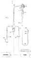
図1から図13は、本発明の一実施の形態を示し、図1は超音波内視鏡の概略構成を説明する図、図2は超音波観測装置の全体構成を示す斜視図、図3は超音波観測装置の正面図、図4は超音波観測装置の背面図、図5は超音波観測装置の分解斜視図、図6は超音波観測装置内の電子部品実装基板ユニットの構成を示す斜視図、図7は別の角度から見た電子部品実装基板ユニットの構成を示す斜視図、図8は電子部品実装基板ユニットの構成を示す側面図、図9は電子部品実装基板ユニットの組立て過程を説明するための斜視図、図10は図9の状態からシールド部材を組み付けた電子部品実装基板ユニットを説明するための斜視図、図11は図10の状態からコントロール基板を組み付けた電子部品実装基板ユニットを説明するための斜視図、図12は電子部品実装基板ユニットの温度上昇を抑制する冷却装置が設けられた状態の電子部品実装基板ユニットの側面図、図13は図12の冷却装置の配置構成を説明するため平面図である。 1 to 13 show an embodiment of the present invention, FIG. 1 is a diagram for explaining a schematic configuration of an ultrasonic endoscope, FIG. 2 is a perspective view showing an overall configuration of an ultrasonic observation apparatus, and FIG. Is a front view of the ultrasonic observation apparatus, FIG. 4 is a rear view of the ultrasonic observation apparatus, FIG. 5 is an exploded perspective view of the ultrasonic observation apparatus, and FIG. 6 is a configuration of an electronic component mounting substrate unit in the ultrasonic observation apparatus. 7 is a perspective view showing the configuration of the electronic component mounting board unit viewed from another angle, FIG. 8 is a side view showing the configuration of the electronic component mounting board unit, and FIG. 9 is an assembly process of the electronic component mounting board unit. FIG. 10 is a perspective view for explaining an electronic component mounting board unit in which a shield member is assembled from the state of FIG. 9, and FIG. 11 is an electronic component mounting in which a control board is assembled from the state of FIG. Perspective for explaining the
図1に示すように本実施形態の超音波医療装置である超音波内視鏡装置1は、超音波内視鏡2と、超音波観測装置3と、カメラコントロールユニット(以下、CCUと略記する)4と、光源装置5と、によって、主に構成されている。尚、超音波観測装置3、及びCCU4は、超音波内視鏡2によって画像化された超音波観察画像、及び内視鏡画像を表示するための、図示しないモニタと接続される。 As shown in FIG. 1, an ultrasonic endoscope apparatus 1 that is an ultrasonic medical apparatus of the present embodiment includes an
超音波内視鏡2は、体腔内に挿入される細長の挿入部8と、この挿入部8の基端に位置する操作部7と、この操作部7の側部から延出するユニバーサルコード10と、で主に構成されている。 The
ユニバーサルコード10の基端部には、光源装置5に接続される内視鏡コネクタ9が設けられている。この内視鏡コネクタ9からは、CCU4に電気コネクタ12を介して着脱自在に接続される電気ケーブル11、及び超音波観測装置3に超音波コネクタ部14を介して着脱自在に接続される超音波ケーブル13が延出している。 An
超音波内視鏡2の挿入部8は、先端側から順に硬質な樹脂部材で形成した先端硬性部21、この先端硬性部21の後端に位置する湾曲自在な湾曲部19、この湾曲部19の後端に位置して操作部7の先端部に至る細径、且つ長尺で可撓性を有する可撓管部18を連設して構成されている。そして、先端硬性部21の先端側には、超音波を送受する複数の電子走査型の超音波トランスデューサを配列した超音波振動子部22が設けられている。 The insertion portion 8 of the
また、超音波内視鏡2の操作部7には、湾曲部19を所望の方向に湾曲制御するアングルノブ16、送気、送水、吸引操作などを行うための各種ボタン15、体腔内に導入する処置具の入り口となる処置具挿入口17等が設けられている。 Further, an
また、超音波振動子部22が設けられた先端硬性部21の先端面には、図示しないが照明光学系を構成する照明用レンズカバー、観察光学系を構成する観察用レンズカバー、吸引口を兼ねる鉗子口、及び送気送水ノズルが配置されている。また、この先端硬性部21は、観察用レンズカバーから導光される撮影光を集光して光電変換するCCD、CMOS等のイメージセンサである、図示しない撮像手段が内蔵されている。 Although not shown, an illumination lens cover that constitutes the illumination optical system, an observation lens cover that constitutes the observation optical system, and a suction port are provided on the distal end surface of the distal
尚、図1においては、超音波観測装置3に接続される電子走査型の超音波内視鏡2を図示して説明したが、これに限定されること無く、本実施の形態の超音波観測装置3には、機械走査型の超音波内視鏡も接続可能となっている。 In FIG. 1, the electronic scanning
次に、図2から図4を用いて、上述した超音波内視鏡2が接続される超音波観測装置3の構成について説明する。
図2、及び図3に示すように、超音波観測装置3は、前面のフロントパネル51に配設された電源スイッチ52と、このフロントパネル51に形成された装置側コネクタ配置面55に並設された2つの異なるタイプの装置側超音波コネクタ部53,54と、を有している。Next, the configuration of the
As shown in FIGS. 2 and 3, the
この装置側コネクタ配置面55において、紙面に向かって見た左側に配置される、本実施の形態の第1の装置側超音波コネクタ部53は、機械走査型の超音波医療機器の超音波コネクタと対を構成する、例えば、96芯タイプのプラグコネクタである。 The first apparatus-side
一方、装置側コネクタ配置面55において、紙面に向かって見た右側に配置される、本実施の形態の第2の装置側超音波コネクタ部54は、電子走査型の超音波医療機器の超音波コネクタと対を構成する、例えば、260芯タイプのプラグコネクタである。 On the other hand, the second apparatus-side
図4に示すように、この超音波観測装置3のリアパネル32には、複数の通信ケーブルなどが接続される接続端子類31、電源ケーブルが接続される電源コネクタ35、及び複数、本実施の形態では4つの冷却ファン33が設けられている。これら4つの冷却ファン33は、後述する電源ユニット64内の温度上昇を抑制するための排気ファンを構成している。 As shown in FIG. 4, the
複数の接続端子類31は、背面板となるリアパネル32の上部側に夫々配設されている。また、電源コネクタ35は、リアパネル32の右下方に配設されている。 The plurality of
さらに、図2に示すように、超音波観測装置3は、両側面、及び上面の筐体外装部を構成するカバーユニット36が設けられている。このカバーユニット36の側面部には、吸気口を構成する通気口45と、持運びの際にユーザが把持するハンドル部39と、が設けられている。 Further, as shown in FIG. 2, the
次に、図5を用いて、本実施の形態の超音波観測装置3の内部構成について以下に説明する。
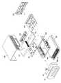
図5に示すように、超音波観測装置3は、外装筐体前面部を構成する上述したフロントパネル51、このフロントパネル51の背面に設けられる2つのインターフェースユニット61,62、外装筐体底面部を構成する板状のベースフレーム63に載置固定された電源ユニット64、一側部に冷却装置であるファンユニットが設けられた電子基板支持台を構成する基板用フレーム65、信号処理基板66、デジタルビームフォーミングユニット(DBFユニット)67、CPUが実装されたコントロール基板68、映像処理基板69、電磁シールドを兼ねた装置内部の領域を区分けする仕切板70、外装筐体背面部を構成する上述したリアパネル32、及び外装筐体両側面部、及び上面部を構成する上述したカバーユニット36から主に構成されている。尚、2つのインターフェースユニット61,62のうち、一方は、機械走査型インターフェースユニット61であり、他方が、電子走査型インターフェースユニット62を構成し、互いが連結固定されている。Next, the internal configuration of the
As shown in FIG. 5, the
つまり、この超音波観測装置3は、フロントパネル51、ベースフレーム63、リアパネル32、及びカバーユニット36により略箱状の外装筐体が形成され、インターフェースユニット61,62、電源ユニット64、基板用フレーム65、信号処理基板66、DBFユニット67、コントロール基板68、仕切板70、及び映像処理基板69が内蔵される構成となっている。 That is, in this
次に、このように超音波観測装置3に内蔵される各電源ユニット64、及び基板の配置について説明する。
先ず、超音波観測装置3の内部において、電源ユニット64は、ベースフレーム63上の最下部となる位置にネジ止め固定される。そして、2つのインターフェースユニット61,62は、電源ユニット64の前方側の位置におけるベースフレーム63上に前方からアクセスされ、ネジ止め固定される。そして、基板用フレーム65は、電源ユニット64上にネジ止め固定される。この電源ユニット64が載置されたベースフレーム63により、ベースユニット58が構成される。Next, the arrangement of the
First, in the
基板用フレーム65へは、先ず、信号処理基板66が上方から下方へ向かった垂直方向に沿ってアクセスされて、ネジ止め固定される。尚、基板用フレーム65には、信号処理基板66が電源ユニット64に対して所定の距離だけ離間する位置に設置するための図示しない、ネジ止め部等が設けられている。すなわち、信号処理基板66は、基板用フレーム65の垂直方向の中途部分で浮いた状態となるように固定される。 First, the
そして、DBFユニット67は、基板用フレーム65の前方側の上方部分に上方から下方へ向かった垂直方向に沿ってアクセスされて、基板用フレーム65の最上部の位置にネジ止め固定される。つまり、DBFユニット67は、信号処理基板66の上方に設置される。これは、DBFユニット67と信号処理基板66とが近傍に位置することにより、互いの電気的な接続を簡易に行えるようにするためである。 Then, the
また、基板用フレーム65の後方側の上方部分には、コントロール基板68がネジ止め固定される。このとき、信号処理基板66の後方縁辺部に設けられた後述する端子板と、映像処理基板69の後方縁辺部に設けられた後述する端子板とに挟まれた状態で信号処理基板66の後方縁辺部の下方部とネジ止めされることで、信号処理基板66から後方側の開口を覆うように架設される仕切板70が固定される。 A
そして、映像処理基板69は、基板用フレーム65の後端部側から電源ユニット64と信号処理基板66との間に向けて、後方から前方へ向かった水平方向に沿ってスライドされて、基板用フレーム65へネジ止め固定される。尚、映像処理基板69は、スライド式の基板ベース体に固定されており、この基板ベース体が基板用フレーム65にネジ止めされることで、一体的に基板用フレーム65に固定配置される。 Then, the
以上に説明したように、これら複数の回路基板部を構成する、信号処理基板66、DBFユニット67、コントロール基板68、及び映像処理基板69は、積層した状態で、ベースユニット58上に設置された基板用フレーム65に固定配置されている(図6から図8参照)。尚、本実施の形態において、信号処理基板66、DBFユニット67、コントロール基板68、及び映像処理基板69がベースユニット58に積層配置された状態が電子部品実装基板ユニット(PCBユニット)59(図11参照)が構成される。 As described above, the
また、PCBユニット59を構成する、各種基板66,68,69、及び各ユニット61,62,67は、夫々が図示しない共通基板により電気的に接続されることで、電気的な回路構成が確立される。また、これらの電気的な接続に対し、本実施の形態では差込型の図示しない基板間コネクタが用いられている。基板間の電気的な接続は、ハーネスを用いても良いが、勿論、差込型の基板間コネクタを用いることで、基板設置固定の際に、同時に電気的な基板間の接続が完了することができる。 In addition, the
さらに、PCBユニット59は、ベースユニット58の電源ユニット64と電気的な接続を、ここでは、図示しないハーネスにより行われており、電源ユニット64からの給電がこのハーネスを介して行われる。尚、本実施の形態のPCBユニット59は、電子部品が実装された各種基板66,68,69、及びDBFユニット67が組み付けられた1つのユニットを構成し、ベースユニット58から取り外して、PCBユニット59全体の交換も行える構成となる。
以上に説明したように、本実施の形態の超音波観測装置3は、PCBユニット59内の複数の回路基板を積層配置することにより、PCBユニット59を小型化することができ、従来に比して、装置全体も小型となる。Further, the
As described above, the
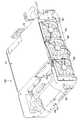
次に、図6から図11に基づいて、小型化したPCBユニット59に内蔵された信号処理基板66、DBFユニット67、コントロール基板68、及び映像処理基板69の構成について説明する。
図6から図8に示すように、DBFユニット67は、両側面に複数の通気口25aが形成され、電磁的な不干渉性を確立するための磁性シールド材から形成された箱状のケース体25と、このケース体25内に配置固定された3つの電子回路基板26,27,28と、によって主に構成されている。Next, the configuration of the
As shown in FIGS. 6 to 8, the
これら3つの電子回路基板26,27,28のうち、ケース体25内の最上部に配置固定される電子回路基板26には、アナログデジタル(AD)コンバータ、デジタルシグナルプロセッサ(DSP)、Field Programmable Gate Array(FPGA)等の電子部品が実装されている。また、ケース体25内の中途部に配置固定される電子回路基板27には、電界効果型トランジスタ(FET)、その他トランジスタ、ダイオード等の電子部品が実装されている。そして、ケース体25内の最下部に配置固定される電子回路基板28には、アンプ、コンデンサ等の電子部品が実装されている。 Of these three
このように、DBFユニット67は、3層に積層配置された3つの電子回路基板26,27,28がケース体25に覆われた構成となっている。これらの電子回路基板26,27,28の合計消費電力は、本実施の形態において、例えば、130Wであり、最上部の電子回路基板26から最下部の電子回路基板28の順で各電子回路基板26,27,28の消費電力が大きいものとなっている。 Thus, the
つまり、DBFユニット67は、ここでは130Wの合計消費電力の内訳が、電子回路基板26に実装されたADコンバータ、DSP、FPGA等の各電子部品の合計した消費電力量が最も多く、次いで、電子回路基板27に実装されたFET、その他トランジスタ、ダイオード等の各電子部品の合計した消費電力量が多い、そして、電子回路基板28に実装されたアンプ、コンデンサ等の各電子部品の合計した消費電力量が最も少ないものとなっている。 That is, in the
このように、DBFユニット67は、消費電力が最も大きな電子回路基板26が発熱量も大きいため、最上部に配置して、消費電力が小さくなるにつれて、発熱量も小さくなるため、消費電力が最も小さな電子回路基板28を最下部に積層配置した構成となっている。 Thus, since the
また、コントロール基板68には、Central Processing Unit(CPU)40、このCPU40上に配置されたヒートシンク41、このヒートシンク41に送風して冷却するCPUファン42、メモリ等が実装されている。このコントロール基板68は、本実施の形態において、例えば、43Wの消費電力となっている。尚、このコントロール基板68には、後方に接続端子類31の一部が配設された端子板43が基板と垂直となるように設けられている。 In addition, a central processing unit (CPU) 40, a
そして、信号処理基板66、及び映像処理基板69は、本実施の形態において、夫々が例えば、13Wの消費電力となっている。尚、映像処理基板69には、後方に接続端子類31の一部が配設された端子板46が基板と垂直となるように設けられている。さらに、映像処理基板69は、基板用フレーム65に後方から前方へ向かった水平方向に沿ってスライドできるよう端子板46と一体形成され、基板の両縁辺部下方に沿って延設されたスライドベース46a上に載置固定されている。 In the present embodiment, each of the
以上から、PCBユニット59は、最も大きな消費電力のDBFユニット67が最上部に配置され、次に大きな消費電力のコントロール基板68をDBFユニット67よりも若干に下方の後方部へ配置され、そして、DBFユニット67の下方に最も小さな消費電力の信号処理基板66、及び映像処理基板69の順で配置された構成となっている。 From the above, in the
尚、信号処理基板66、及び映像処理基板69は、ここでは同一消費電力であるため、配置位置を入れ替えても勿論、構わないし、消費電力が異なる場合は、消費電力が大きいものを上部側に配置すれば良い。 Since the
以上のように構成され、ベースユニット58、及びPCBユニット59が電気的に接続された後に、フロントパネル51、カバーユニット36、及びリアパネル32がネジ止め固定されることにより、図2に示したような、本実施の形態の超音波観測装置3が組み立てられた状態となる。 After the
このように組み立てられた超音波観測装置3の使用可能状態において、PCBユニット59は、前後に沿って3つの発熱領域a,b,cに仕切られた断面空間が形成される。
具体的には、図8から図11に示すように、DBFユニット67の磁性シールド材から形成されたケース体25によって囲まれた領域が第1の発熱領域aとなる。すなわち、超音波観測装置3の駆動時に最も消費電力が大きなDBFユニット67内の各種電子部品が発熱源となり、超音波観測装置3内の仕切られた最も温度が上昇する領域が第1の発熱領域aとなっている。In the usable state of the
Specifically, as shown in FIGS. 8 to 11, a region surrounded by the
そして、図8、及び図11に示すように、上部側がDBFユニット67、及びカバーユニット36、下部側が信号処理基板66、及び磁性シールド材から形成された仕切板70、後方側がコントロール基板68の端子板43、及び前方側が基板用フレーム65から垂直上方に延出するように固定され、磁性シールド材から形成された板体71によって囲まれた領域が第2の発熱領域bとなる。すなわち、超音波観測装置3の駆動時に2番目に消費電力が大きなコントロール基板68の各種電子部品と、ここでは最も消費電力が小さな信号処理基板66の各種電子部品と、が合わさって発熱源となり、超音波観測装置3内で仕切られた2番目に温度が上昇する領域が第2の発熱領域bとなっている。 8 and 11, the upper side is a
さらに、図8、及び図10に示すように、上部側が信号処理基板66、及び仕切板70、下部側が基板用フレーム65、後方側が映像処理基板69の端子板46、及び前方側が板体71によって囲まれた領域が第3の発熱領域cとなる。すなわち、超音波観測装置3の駆動時に、最も消費電力が小さな映像処理基板69の各種電子部品が発熱源となり、超音波観測装置3内で仕切られた3番目に温度が上昇する領域が第3の発熱領域cとなっている。 Further, as shown in FIGS. 8 and 10, the upper side is a
尚、図8に示すように、基板用フレーム65に固定された板体71は、上部端面全長にわたって、DBFユニット67の底面に接触して隙間が生じないようにするためのガスケット72が設けられている。このガスケット72は、電磁シールドを兼ねており、超音波観測装置3から外部機器へ電磁的に干渉して、動作を阻害したりして、電磁妨害を生じさせないようにする電磁環境適合性(EMC)を確保するためのものである。 As shown in FIG. 8, the
また、仕切板70は、電磁波シールド材から形成されており、映像処理基板69と、この映像処理基板69の上部に設けられた、特にコントロール基板68と、の電磁的な干渉を防止することができ、各回路構成に電磁ノイズ等の発生を抑制するためのシールドを兼ねている。 Further, the
以上のように、本実施の形態の超音波観測装置3のPCBユニット59は、フロントパネル51、ベースフレーム63、リアパネル32、及びカバーユニット36により形成される外装筐体内部が3つの発熱領域a,b,cで仕切られ、図12、及び図13示すように、基板用フレーム65の一側面に並設された3つのファン(送風機)81,82,83を有している。これら3つのファン81,82,83は、3つの発熱領域a,b,c内の温度を各電子部品の使用環境温度以下に保つように温度上昇した空気を排気することにより冷却する同一の送風能力を備えた冷却装置を構成している。 As described above, the
また、3つのファン81,82,83は、PCBユニット59の長手方向(図中X軸方向)に沿って所定の距離で離間するYa,Yb,Ycに示す3つの軸上に中心(多翼の回動中心)が夫々位置するように基板用フレーム65の一側面に並べて配設されている。 The three
また、本実施の形態のPCBユニット59は、DBFユニット67、コントロール基板68と信号処理基板66、及び映像処理基板69の夫々の各種電子部品の合計消費電力量が、鉛直上方(図中y軸に沿った上方)から鉛直下方(図中y軸に沿った下方)へ向かって、順に少なくなるように積層するように仕切られた3つの発熱領域a,b,cが発熱する熱量も順に少なくなる。 In the
そのため、第1のファン81、第2のファン82、及び第3のファン83は、図13に示すように、効率良く3つの発熱領域a,b,cの温度上昇を抑制できるように、フロント側からリヤ側に向けて、夫々の中心(多翼の回動中心)位置が鉛直下方(図中y軸に沿った下方)へ段階的にずれた位置に配置されている。換言すると、第1のファン81の中心(多翼81aの回動中心)がXa軸上に位置し、第2のファン82の中心(多翼82aの回動中心)がXa軸よりもY軸に沿った鉛直下方側のXb軸上に位置し、第3のファン83の中心(多翼83aの回動中心)がXb軸よりもY軸に沿った鉛直下方側のXc軸上に位置している。 Therefore, as shown in FIG. 13, the
さらに詳しく説明すると、最もフロント側に設けられた第1のファン81は、最も温度が上昇する第1の発熱領域a、及び次に温度が上昇する第2の発熱領域bの空気を排気するためのもので、多翼81aにより空気を排気する開口81bの表面積のおおよそ60%が第1の発熱領域aにかかり、開口81bの残りの表面積のおおよそ40%が第2の発熱領域bにかかるように配置されている。 More specifically, the
また、中央に設けられた第2のファン82は、第1の発熱領域a、第2の発熱領域b、及び最も温度上昇が低い第3の発熱領域cの空気を排気するためのもので、多翼82aにより空気を排気する開口82bの表面積のおおよそ47%が第1の発熱領域aにかかり、開口81bの残りの表面積のおおよそ53%が第2の発熱領域b、及び第3の発熱領域cにかかるように配置されている。 The
この第2のファン82は、基板用フレーム65の一側面の限られた配置面積に3つのファン81,82,83を並設するため、他の2つのファン81,83に対して、若干、多翼82a回りに斜めに配置されている。尚、第2のファン82は、映像処理基板69の一側部上方で、リヤ側からフロント側に沿った映像処理基板69の長さLに合わせて側部が略一致するように配置されている。 The
さらに、最もリヤ側に設けられた第3のファン83は、第2の発熱領域b、及び第3の発熱領域cの空気を排気するためのもので、多翼83aにより空気を排気する開口83bの表面積のおおよそ50%が第2の発熱領域bにかかり、開口83bの残りの表面積のおおよそ50%が第3の発熱領域cにかかるように配置されている。 Further, the
このように、例えば、130Wで駆動する電子部品に応じた発熱量により最も温度上昇する第1の発熱領域a内の空気は、第1、及び第2のファン81,82により、ファン1つが備える能力以上の、およそ、107%(=60%+47%)に匹敵した送風能力で強制排気される。 Thus, for example, the air in the first heat generation region a that rises the most by the heat generation amount corresponding to the electronic component driven at 130 W is provided by one fan by the first and
つまり、超音波観測装置3のPCBユニット59は、3つの発熱領域a,b,cの中で、最も合計消費電力量の多い各電子部品により最も温度上昇する第1の発熱領域aを備えたDBFユニット67内の空気を強制排気させて、DBFユニット67内の各電子部品の使用環境温度以下に保つように、第1、及び第2のファン81,82が設けられた装置内冷却構造となっている。 That is, the
尚、例えば、56W(=43W+13W)で駆動する電子部品に応じた発熱量により2番目に温度上昇する第2の発熱領域b内の空気は、第1、第2、及び第3のファン81,82,83により強制排気される。そして、例えば、13Wで駆動する電子部品に応じた発熱量により最も温度上昇が低くなる第3の発熱領域c内の空気は、第2、及び第3のファン82,83により強制排気される。 Note that, for example, the air in the second heat generation region b where the temperature rises second by the heat generation amount corresponding to the electronic component driven at 56 W (= 43 W + 13 W) is the first, second, and
これにより、超音波観測装置3のPCBユニット59は、第2、及び第3のファン82,83によって、第2の発熱領域a内、及び第3の発熱領域c内の空気を強制排気させて、コントロール基板68と信号処理基板66、及び映像処理基板69に実装される各電子部品の使用環境温度以下を十分に保つことができる。 Thereby, the
以上のように構成された本実施の形態の超音波観測装置3は、外形全体の小型化に伴って、内部スペースに制約が生じるため、複数の基板を積層して配置すると共に、最も消費電力が大きく、高温となる基板を最上部に配置し、各種基板間における他の実装電子部品に熱的影響をできるだけ与えないようにし、使用環境温度以下となるように効率よく、温度上昇した空気を強制排気できる最適な位置に3つのファン81,82,83を配置した装置内冷却構造を備えている。 In the
以上の説明により、本実施の形態の超音波観測装置3は、小型化を図り、装置内部の小さなスペースに配置した複数の基板に実装された各種電子部品からの放熱による装置内部の温度上昇を抑制して、各電子部品の使用環境温度以下となるように効率良く冷却することができる装置内冷却構造を備えた構成とすることができる。 As described above, the
以上の実施の形態に記載した発明は、その実施の形態、及び変形例に限ることなく、その他、実施段階ではその要旨を逸脱しない範囲で種々の変形を実施し得ることが可能である。さらに、上記実施の形態には、種々の段階の発明が含まれており、開示される複数の構成要件における適宜な組合せにより種々の発明が抽出され得る。 The invention described in the above embodiment is not limited to the embodiment and modifications, and various modifications can be made without departing from the scope of the invention in the implementation stage. Further, the above embodiments include inventions at various stages, and various inventions can be extracted by appropriately combining a plurality of disclosed constituent elements.
例えば、実施の形態に示される全構成要件から幾つかの構成要件が削除されても、発明が解決しようとする課題で述べた課題が解決でき、発明の効果で述べられている効果が得られる場合には、この構成要件が削除された構成が発明として抽出され得る。 For example, even if some constituent elements are deleted from all the constituent elements shown in the embodiment, the problem described in the problem to be solved by the invention can be solved, and the effect described in the effect of the invention can be obtained. In some cases, a configuration from which this configuration requirement is deleted can be extracted as an invention.
1・・・超音波内視鏡装置
2・・・超音波内視鏡
3…超音波観測装置
5…光源装置
25…ケース体
25a…通気口
26…第1の電子回路基板
27…第2の電子回路基板
28…第3の電子回路基板
31…接続端子類
32…リアパネル
33…冷却ファン
35…電源コネクタ
36…カバーユニット
39…ハンドル部
41…ヒートシンク
42…ファン
43…端子板
45…通気口
46a…スライドベース
46…端子板
59…PCBユニット
65…基板用フレーム
66…信号処理基板
67…DBFユニット
68…コントロール基板
69…映像処理基板
70…仕切板
71…板体
72…ガスケット
81…第1のファン
82…第2のファン
83…第3のファン
a…第1の発熱領域
b…第2の発熱領域
c…第3の発熱領域DESCRIPTION OF SYMBOLS 1 ...
Claims (7)
Translated fromJapanese前記複数の回路基板部と共に、前記フレームを覆う外装筐体と、
前記複数の回路基板部の発熱による前記外装筐体内の温度上昇を抑制する複数の冷却装置と、
前記複数の回路基板部のうち、最も合計消費電力量の多い該回路基板部を囲むように仕切った発熱領域と、
を備え、
前記発熱領域内の温度上昇を1つの前記冷却装置の能力以上で抑制するように前記複数の冷却装置を配置したことを特徴とする装置内冷却構造。A frame in which a plurality of circuit board parts on which various electronic components are mounted according to function are stacked;
Along with the plurality of circuit board parts, an exterior housing that covers the frame;
A plurality of cooling devices for suppressing temperature rise in the exterior casing due to heat generation of the plurality of circuit board parts;
Among the plurality of circuit board parts, a heat generation area partitioned so as to surround the circuit board part having the largest total power consumption,
With
An in-device cooling structure in which the plurality of cooling devices are arranged so as to suppress a temperature rise in the heat generation region beyond the capacity of one cooling device.
該別の発熱領域内の温度上昇も前記複数の冷却装置によって抑制することを特徴とする請求項1、又は請求項2に記載の装置内冷却構造。Having another heat generation area partitioned so as to surround the circuit board part different from the circuit board part having the largest total power consumption divided into the heat generation area,
The in-device cooling structure according to claim 1, wherein a temperature rise in the another heat generation region is also suppressed by the plurality of cooling devices.
該3つの送風機が前記フレームの一側面に水平方向に並設されていることを特徴とする請求項1から請求項3のいずれか1項に記載の装置内冷却構造。The plurality of cooling devices are composed of three blowers having the same blowing capacity,
The in-device cooling structure according to any one of claims 1 to 3, wherein the three blowers are juxtaposed in a horizontal direction on one side surface of the frame.
Priority Applications (4)
| Application Number | Priority Date | Filing Date | Title |
|---|---|---|---|
| JP2008186309AJP5164706B2 (en) | 2008-07-17 | 2008-07-17 | In-device cooling structure and ultrasonic observation device |
| EP09008980AEP2145584B1 (en) | 2008-07-17 | 2009-07-09 | Interior cooling structure and ultrasound imaging apparatus |
| AT09008980TATE511795T1 (en) | 2008-07-17 | 2009-07-09 | INTERIOR COOLING STRUCTURE AND ULTRASONIC IMAGING DEVICE |
| US12/504,160US7920381B2 (en) | 2008-07-17 | 2009-07-16 | Interior cooling structure and ultrasound imaging apparatus |
Applications Claiming Priority (1)
| Application Number | Priority Date | Filing Date | Title |
|---|---|---|---|
| JP2008186309AJP5164706B2 (en) | 2008-07-17 | 2008-07-17 | In-device cooling structure and ultrasonic observation device |
Publications (2)
| Publication Number | Publication Date |
|---|---|
| JP2010022536A JP2010022536A (en) | 2010-02-04 |
| JP5164706B2true JP5164706B2 (en) | 2013-03-21 |
Family
ID=41041022
Family Applications (1)
| Application Number | Title | Priority Date | Filing Date |
|---|---|---|---|
| JP2008186309AActiveJP5164706B2 (en) | 2008-07-17 | 2008-07-17 | In-device cooling structure and ultrasonic observation device |
Country Status (4)
| Country | Link |
|---|---|
| US (1) | US7920381B2 (en) |
| EP (1) | EP2145584B1 (en) |
| JP (1) | JP5164706B2 (en) |
| AT (1) | ATE511795T1 (en) |
Families Citing this family (18)
| Publication number | Priority date | Publication date | Assignee | Title |
|---|---|---|---|---|
| CN101808489A (en)* | 2009-02-17 | 2010-08-18 | 鸿富锦精密工业(深圳)有限公司 | Heat dissipating system and wind deflectors thereof |
| EP2339905B1 (en) | 2009-12-22 | 2012-06-27 | ABB Oy | Power electronic apparatuses with cooling arrangements |
| EP2339906B1 (en)* | 2009-12-22 | 2012-06-27 | ABB Oy | Power electronic apparatus with cooling arrangement |
| KR20140006392A (en)* | 2012-07-05 | 2014-01-16 | 엘에스산전 주식회사 | Electronic component box for vehicle |
| CN103809711B (en)* | 2012-11-12 | 2017-07-14 | 英业达科技有限公司 | Electronic installation |
| CN103997871A (en)* | 2013-02-19 | 2014-08-20 | 鸿富锦精密工业(深圳)有限公司 | Electronic device |
| RU2569492C1 (en)* | 2014-07-04 | 2015-11-27 | Акционерное общество "Государственный Рязанский приборный завод" | Air-cooled electronic unit |
| WO2016007667A1 (en)* | 2014-07-09 | 2016-01-14 | Edan Instruments, Inc. | Modular and portable ultrasound systems and methods |
| CN105559818B (en)* | 2014-10-10 | 2018-06-01 | 重庆海扶医疗科技股份有限公司 | A kind of ultrasonic detection equipment and method |
| CN104586432B (en)* | 2015-01-27 | 2017-12-15 | 深圳市理邦精密仪器股份有限公司 | Car-type ultrasonic diagnostic equipment and its cabinet |
| US10528096B2 (en) | 2015-06-01 | 2020-01-07 | International Business Machines Corporation | Optimizing cooling energy |
| CN104881101B (en)* | 2015-06-09 | 2018-06-19 | 英业达科技有限公司 | Electronic device |
| US10184478B2 (en)* | 2016-05-12 | 2019-01-22 | In Win Development, Inc. | Fan device with modular functionality |
| US11019748B2 (en)* | 2017-12-22 | 2021-05-25 | Seagate Technology Llc | Suspended fan modules |
| US10908270B2 (en)* | 2018-01-18 | 2021-02-02 | Fujifilm Sonosite, Inc. | Portable ultrasound imaging system with active cooling |
| JP7216882B2 (en)* | 2018-12-25 | 2023-02-02 | スター精密株式会社 | Machine tool control panel |
| CN114945316A (en)* | 2020-01-29 | 2022-08-26 | 奥林巴斯株式会社 | Cooling device for endoscope |
| CN111935923B (en)* | 2020-09-11 | 2022-04-01 | 山东万盛电气有限公司 | Explosion-proof electrical cabinet |
Family Cites Families (42)
| Publication number | Priority date | Publication date | Assignee | Title |
|---|---|---|---|---|
| DE3837744A1 (en)* | 1988-11-07 | 1990-05-10 | Knuerr Mechanik Ag | ASSEMBLY CARRIERS FOR PCBS WITH ELECTRONIC COMPONENTS |
| JPH04231929A (en)* | 1990-12-28 | 1992-08-20 | Fuji Photo Optical Co Ltd | Electronic endoscope device |
| JPH0661674A (en)* | 1991-08-19 | 1994-03-04 | Nippon Telegr & Teleph Corp <Ntt> | Electronic device mounting structure |
| JP2596682B2 (en)* | 1992-09-08 | 1997-04-02 | 株式会社日立製作所 | Electronic equipment cooling device |
| JP3254756B2 (en)* | 1992-10-13 | 2002-02-12 | 株式会社日立製作所 | Electronic equipment |
| US5796580A (en)* | 1993-04-13 | 1998-08-18 | Hitachi, Ltd. | Air-cooled information processing apparatus having cooling air fan, sub-fan, and plural separated cooling air flow channels |
| US5446619A (en)* | 1993-08-12 | 1995-08-29 | Compaq Computer Corp. | Card extender unit for computer |
| JPH07221477A (en)* | 1994-02-09 | 1995-08-18 | Fujitsu Ltd | Cooling structure for printed wiring board mounting parts |
| JPH09325831A (en)* | 1996-06-04 | 1997-12-16 | Pfu Ltd | Module heat dissipation structure |
| US6331722B1 (en)* | 1997-01-18 | 2001-12-18 | Semiconductor Energy Laboratory Co., Ltd. | Hybrid circuit and electronic device using same |
| US5813243A (en)* | 1997-04-04 | 1998-09-29 | Micron Electronics, Inc. | Chambered forced cooling system |
| US5923531A (en)* | 1997-10-14 | 1999-07-13 | International Business Machines Corporation | Enhanced circuit board arrangement for a computer |
| JPH11186764A (en)* | 1997-12-25 | 1999-07-09 | Mitsubishi Electric Corp | PCB cooling structure |
| JP3408424B2 (en)* | 1998-07-28 | 2003-05-19 | 日本電気株式会社 | Electronic equipment cooling structure |
| US6198628B1 (en)* | 1998-11-24 | 2001-03-06 | Unisys Corporation | Parallel cooling of high power devices in a serially cooled evironment |
| JP2000174474A (en)* | 1998-12-02 | 2000-06-23 | Nippon Columbia Co Ltd | Cooling device of electronic equipment |
| US6061237A (en)* | 1998-12-21 | 2000-05-09 | Dell Usa, L.P. | Computer with an improved cooling system and a method for cooling a computer |
| US6034870A (en)* | 1999-01-27 | 2000-03-07 | Sun Microsystems, Inc. | Computer system having a highly efficient forced air cooling subsystem |
| US6359779B1 (en)* | 1999-04-05 | 2002-03-19 | Western Digital Ventures, Inc. | Integrated computer module with airflow accelerator |
| US6972953B1 (en)* | 1999-10-04 | 2005-12-06 | Apple Computer, Inc. | Thermal management system |
| JP2001338486A (en)* | 2000-05-25 | 2001-12-07 | Hitachi Ltd | Information storage device |
| JP3917800B2 (en)* | 2000-06-02 | 2007-05-23 | オリンパス株式会社 | Ultrasonic observation equipment |
| US6597569B1 (en)* | 2000-06-29 | 2003-07-22 | Intel Corporation | Partitioned computer platform |
| US6400567B1 (en)* | 2000-10-19 | 2002-06-04 | Fujitsu Network Communications, Inc. | Equipment enclosure having separate compartments cooled by separate cooling airflows |
| TW484721U (en)* | 2000-11-06 | 2002-04-21 | Giga Byte Tech Co Ltd | Improved airflow guiding structure of server |
| JP4071627B2 (en)* | 2000-12-11 | 2008-04-02 | 富士通株式会社 | Electronic equipment unit |
| US6459579B1 (en)* | 2001-01-03 | 2002-10-01 | Juniper Networks, Inc. | Apparatus and method for directing airflow in three dimensions to cool system components |
| US6567271B2 (en)* | 2001-03-05 | 2003-05-20 | Toshiba America Information Systems, Inc. | Circuit board interconnection and fan-mounting assembly for convective cooling |
| US6544311B1 (en)* | 2002-04-17 | 2003-04-08 | Ag Communication Systems Corporation | Chassis thermal zones |
| JP4312424B2 (en)* | 2002-06-14 | 2009-08-12 | 株式会社日立製作所 | Disk array device |
| US7036027B2 (en)* | 2002-10-21 | 2006-04-25 | Sun Microsystems, Inc. | Computer system layout and cooling configuration |
| US6795314B1 (en)* | 2003-03-25 | 2004-09-21 | Hewlett-Packard Development Company, L.P. | Removable fan module and electronic device incorporating same |
| US7035102B2 (en)* | 2004-01-08 | 2006-04-25 | Apple Computer, Inc. | Apparatus for air cooling of an electronic device |
| JP2006020755A (en) | 2004-07-07 | 2006-01-26 | Toshiba Corp | Portable medical device |
| US7061761B2 (en)* | 2004-07-30 | 2006-06-13 | Hewlett-Packard Development Company, L.P. | System and method for cooling components in an electronic device |
| JP4312235B2 (en)* | 2004-11-16 | 2009-08-12 | 富士通株式会社 | Communication device and rack structure |
| JP2006156871A (en)* | 2004-12-01 | 2006-06-15 | Fuji Electric Systems Co Ltd | Locker type cooling system |
| EP1672642A1 (en)* | 2004-12-20 | 2006-06-21 | Harman Becker Automotive Systems GmbH | Electronic built-in system |
| JP4765095B2 (en)* | 2005-01-19 | 2011-09-07 | 富士電機株式会社 | Box device |
| FR2910227A1 (en)* | 2006-12-18 | 2008-06-20 | Sagem Defense Securite | INTEGRATED ELECTRONIC COMPONENT DEVICE PROVIDED WITH A VENTILATED ZONE SEPARATION PAN |
| US7408774B1 (en)* | 2007-03-06 | 2008-08-05 | International Business Machines Corporation | Real time adaptive active fluid flow cooling |
| JP4350767B2 (en)* | 2007-03-30 | 2009-10-21 | オリンパスメディカルシステムズ株式会社 | Medical equipment |
- 2008
- 2008-07-17JPJP2008186309Apatent/JP5164706B2/enactiveActive
- 2009
- 2009-07-09EPEP09008980Apatent/EP2145584B1/ennot_activeNot-in-force
- 2009-07-09ATAT09008980Tpatent/ATE511795T1/ennot_activeIP Right Cessation
- 2009-07-16USUS12/504,160patent/US7920381B2/enactiveActive
Also Published As
| Publication number | Publication date |
|---|---|
| US20100014250A1 (en) | 2010-01-21 |
| EP2145584B1 (en) | 2011-06-08 |
| JP2010022536A (en) | 2010-02-04 |
| US7920381B2 (en) | 2011-04-05 |
| EP2145584A1 (en) | 2010-01-20 |
| ATE511795T1 (en) | 2011-06-15 |
Similar Documents
| Publication | Publication Date | Title |
|---|---|---|
| JP5164706B2 (en) | In-device cooling structure and ultrasonic observation device | |
| JP4350767B2 (en) | Medical equipment | |
| CN109414250B (en) | Ultrasonic endoscope | |
| CN107149460B (en) | Endoscope with a detachable handle | |
| CN109414251B (en) | Ultrasonic endoscope and method for manufacturing same | |
| JP5775984B1 (en) | Endoscope device | |
| CN109328037B (en) | Ultrasonic endoscope | |
| US11076838B2 (en) | Ultrasonic endoscope | |
| JP6596158B2 (en) | Ultrasound endoscope | |
| JP5030688B2 (en) | Case mechanism and ultrasonic observation apparatus | |
| JP2019013388A (en) | Electronic equipment | |
| JP2011200338A (en) | Electronic endoscope | |
| WO2014083967A1 (en) | Board structure | |
| JP2014210041A (en) | Imaging device and electronic endoscope | |
| JP7233933B2 (en) | Electronic endoscope and electronic endoscope system | |
| JP2014113350A (en) | Endoscope and endoscope system | |
| JP2014210040A (en) | Imaging device and electronic endoscope | |
| JP7398400B2 (en) | Endoscopic imaging devices and endoscopes | |
| JP2019016671A (en) | Substrate support structure for electronic equipment | |
| JP2008040104A (en) | Endoscopic device | |
| JP2020010764A (en) | Medical instrument for endoscope | |
| JP2009279299A (en) | Endoscope | |
| WO2015137158A1 (en) | Electrical apparatus |
Legal Events
| Date | Code | Title | Description |
|---|---|---|---|
| A621 | Written request for application examination | Free format text:JAPANESE INTERMEDIATE CODE: A621 Effective date:20110318 | |
| A977 | Report on retrieval | Free format text:JAPANESE INTERMEDIATE CODE: A971007 Effective date:20121120 | |
| TRDD | Decision of grant or rejection written | ||
| A01 | Written decision to grant a patent or to grant a registration (utility model) | Free format text:JAPANESE INTERMEDIATE CODE: A01 Effective date:20121204 | |
| A61 | First payment of annual fees (during grant procedure) | Free format text:JAPANESE INTERMEDIATE CODE: A61 Effective date:20121218 | |
| FPAY | Renewal fee payment (event date is renewal date of database) | Free format text:PAYMENT UNTIL: 20151228 Year of fee payment:3 | |
| R151 | Written notification of patent or utility model registration | Ref document number:5164706 Country of ref document:JP Free format text:JAPANESE INTERMEDIATE CODE: R151 | |
| FPAY | Renewal fee payment (event date is renewal date of database) | Free format text:PAYMENT UNTIL: 20151228 Year of fee payment:3 | |
| S111 | Request for change of ownership or part of ownership | Free format text:JAPANESE INTERMEDIATE CODE: R313111 | |
| R350 | Written notification of registration of transfer | Free format text:JAPANESE INTERMEDIATE CODE: R350 | |
| S531 | Written request for registration of change of domicile | Free format text:JAPANESE INTERMEDIATE CODE: R313531 | |
| R350 | Written notification of registration of transfer | Free format text:JAPANESE INTERMEDIATE CODE: R350 | |
| R250 | Receipt of annual fees | Free format text:JAPANESE INTERMEDIATE CODE: R250 | |
| R250 | Receipt of annual fees | Free format text:JAPANESE INTERMEDIATE CODE: R250 | |
| R250 | Receipt of annual fees | Free format text:JAPANESE INTERMEDIATE CODE: R250 | |
| R250 | Receipt of annual fees | Free format text:JAPANESE INTERMEDIATE CODE: R250 | |
| R250 | Receipt of annual fees | Free format text:JAPANESE INTERMEDIATE CODE: R250 | |
| R250 | Receipt of annual fees | Free format text:JAPANESE INTERMEDIATE CODE: R250 | |
| R250 | Receipt of annual fees | Free format text:JAPANESE INTERMEDIATE CODE: R250 |