JP5157201B2 - Semiconductor device - Google Patents
Semiconductor deviceDownload PDFInfo
- Publication number
- JP5157201B2 JP5157201B2JP2007060809AJP2007060809AJP5157201B2JP 5157201 B2JP5157201 B2JP 5157201B2JP 2007060809 AJP2007060809 AJP 2007060809AJP 2007060809 AJP2007060809 AJP 2007060809AJP 5157201 B2JP5157201 B2JP 5157201B2
- Authority
- JP
- Japan
- Prior art keywords
- semiconductor
- semiconductor device
- layer
- semiconductor layer
- region
- Prior art date
- Legal status (The legal status is an assumption and is not a legal conclusion. Google has not performed a legal analysis and makes no representation as to the accuracy of the status listed.)
- Active
Links
Images


Classifications
- H—ELECTRICITY
- H10—SEMICONDUCTOR DEVICES; ELECTRIC SOLID-STATE DEVICES NOT OTHERWISE PROVIDED FOR
- H10D—INORGANIC ELECTRIC SEMICONDUCTOR DEVICES
- H10D12/00—Bipolar devices controlled by the field effect, e.g. insulated-gate bipolar transistors [IGBT]
- H10D12/411—Insulated-gate bipolar transistors [IGBT]
- H10D12/441—Vertical IGBTs
- H—ELECTRICITY
- H10—SEMICONDUCTOR DEVICES; ELECTRIC SOLID-STATE DEVICES NOT OTHERWISE PROVIDED FOR
- H10D—INORGANIC ELECTRIC SEMICONDUCTOR DEVICES
- H10D8/00—Diodes
- H—ELECTRICITY
- H10—SEMICONDUCTOR DEVICES; ELECTRIC SOLID-STATE DEVICES NOT OTHERWISE PROVIDED FOR
- H10D—INORGANIC ELECTRIC SEMICONDUCTOR DEVICES
- H10D84/00—Integrated devices formed in or on semiconductor substrates that comprise only semiconducting layers, e.g. on Si wafers or on GaAs-on-Si wafers
- H10D84/60—Integrated devices formed in or on semiconductor substrates that comprise only semiconducting layers, e.g. on Si wafers or on GaAs-on-Si wafers characterised by the integration of at least one component covered by groups H10D10/00 or H10D18/00, e.g. integration of BJTs
- H10D84/611—Combinations of BJTs and one or more of diodes, resistors or capacitors
- H10D84/613—Combinations of vertical BJTs and one or more of diodes, resistors or capacitors
- H10D84/617—Combinations of vertical BJTs and only diodes
Landscapes
- Metal-Oxide And Bipolar Metal-Oxide Semiconductor Integrated Circuits (AREA)
Description
Translated fromJapanese本発明は、IGBTセルとダイオードセルが、一つの半導体基板に併設されてなる半導体装置に関する。The present invention, IGBT cell and the diode cell, relatesto a semiconductor device formed by features on a single semiconductor substrate.
モータ等の負荷を駆動するためのインバータ回路は、直流と交流の交換機であり、直流電圧を交流電圧に変換して、負荷であるモータ等に給電する。誘導性のモータを駆動するためのインバータ回路は、例えば、スイッチング素子である絶縁ゲートバイポーラトランジスタ(IGBT、Insulated Gate BipolarTransistor)とフリーホイールダイオード(FWD)で構成される。ここで、IGBTは、スイッチング素子として用いられ、FWDは、IGBTのオフ中にモータに流れる電流を迂回還流させ、モータを流れる電流自体がIGBTのスイッチングにより変化しないようにしている。より具体的には、直流電源とモータを繋ぎ、モータに電圧を印加していたIGBTがオフすると、モータを流れていた電流がモータのLに蓄積されているエネルギーによりFWDを通って直流電流を逆流し、モータは、逆の直流電圧が印加されているのと等価な状態となる。これによって、モータの電流はIGBTのスイッチングにより急激に遮断することがないため、直流電源からスイッチングにより実質的に交流電圧を給電することができる。 An inverter circuit for driving a load such as a motor is a direct-current and alternating-current exchanger, converts a direct-current voltage into an alternating-current voltage, and supplies power to the load motor and the like. An inverter circuit for driving an inductive motor includes, for example, an insulated gate bipolar transistor (IGBT) that is a switching element and a free wheel diode (FWD). Here, the IGBT is used as a switching element, and the FWD bypasses and recirculates the current flowing through the motor while the IGBT is off, so that the current flowing through the motor itself does not change due to the switching of the IGBT. More specifically, when the IGBT that connected the DC power source and the motor and applied the voltage to the motor is turned off, the current flowing through the motor is passed through the FWD by the energy accumulated in the L of the motor and the DC current is The motor flows in the reverse direction, and the motor is in a state equivalent to the application of the reverse DC voltage. Thus, since the motor current is not suddenly interrupted by the switching of the IGBT, an AC voltage can be substantially supplied from the DC power supply by the switching.
上記インバータ回路の構成要素であるIGBTは、いわゆるパンチスルー(PT)型IGBT、ノンパンチスルー(NPT)型IGBT、および両者の中間的存在で特開2004−103982号公報(特許文献1)に開示されているフィールドストップ(FS)型IGBTに大別できる。PT型IGBTは、P導電型(P+)の厚い基板をコレクタ層とし、N導電型(N−)のドリフト層との間にN導電型(N+)のバッファ層を挿入した構造となっている。NPT型IGBTは、ドリフト層として機能する薄いN導電型(N−)の基板(ボディ層)の裏面にP導電型(P+)のコレクタ層が形成された構造となっている。また、FS型IGBTは、NPT型IGBTのドリフト層とコレクタ層の間にフィールドストップ(FS)層と呼ぶN導電型のキャリア濃度を低く設計したバッファ層を挿入して、ドリフト層であるN導電型(N−)の基板(ボディ層)をさらに薄くした構造となっている。 The IGBT, which is a component of the inverter circuit, is disclosed in Japanese Patent Application Laid-Open No. 2004-103982 (Patent Document 1) as a so-called punch-through (PT) type IGBT, non-punch-through (NPT) type IGBT, and an intermediate between them. The field stop (FS) type IGBT can be roughly classified. The PT type IGBT has a structure in which a thick substrate of P conductivity type (P +) is used as a collector layer and an N conductivity type (N +) buffer layer is inserted between the N conductivity type (N−) drift layer. . The NPT type IGBT has a structure in which a P conductivity type (P +) collector layer is formed on the back surface of a thin N conductivity type (N−) substrate (body layer) functioning as a drift layer. In the FS type IGBT, a buffer layer designed to have a low N conductivity type carrier concentration, called a field stop (FS) layer, is inserted between the drift layer and the collector layer of the NPT type IGBT, and the N conductivity is the drift layer. The type (N−) substrate (body layer) is further thinned.
インバータ回路においては、前述したように、IGBTとFWDが組み合わせて用いられる。近年では、上記インバータ回路の小型化を目的として、IGBTセルとダイオードセルが一つの半導体基板に併設されてなる半導体装置が検討されており、このような半導体装置が、例えば、特開2005−57235号公報(特許文献2)と特開平6−196705号公報(特許文献3)に開示されている。特許文献2には、NPT型IGBTがダイオードと共に形成されてなる半導体装置が開示されており、特許文献3には、それぞれ、NPT型IGBTおよびPT型IGBTがダイオードと共に形成されてなる半導体装置が開示されている。
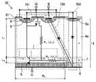
図14は、特許文献3に開示された半導体装置と同様のPT型IGBTがダイオードと共に形成されてなる半導体装置で、従来の半導体装置90の模式的な断面図である。 FIG. 14 is a schematic cross-sectional view of a
図14に示す半導体装置90は、IGBTセルとダイオードセルが一つの半導体基板1に併設されており、図中に一点鎖線で囲った領域90iがIGBTセルに相当し、二点鎖線で囲った領域90dがダイオードセルに相当する。図中には、それぞれの領域に対して、等価回路記号を重ねて示してある。IGBT90iは、MOSトランジスタ90mとバイポーラトランジスタ90bが図のように接続された構成として表され、MOSトランジスタ90mを流れる電流がバイポーラトランジスタ90bのベース電流となる。 In the
図14の半導体装置90において、半導体基板1の主面から裏面近くに至るN導電型(N−)の第1半導体層(ボディ層)1aは、IGBT90iとダイオード90dのキャリアのドリフト層である。半導体基板1の裏面側の表層部に形成されたP導電型(P+)の第2半導体層2は、IGBT90iのコレクタ層(バイポーラトランジスタ90bのエミッタ層)である。また、第2半導体層2を覆って形成されたN導電型(N+)の第3半導体層3は、第2半導体層2に隣接して裏面電極に接続する領域3aがダイオード90dのカソード電極接続層として機能し、第2半導体層2上の領域3bがIGBT90iのバッファ層3bとして機能する。 In the
図14の半導体装置90に形成されているIGBTは、バッファ層3bを有するPT型IGBTの構造となっており、キャリアのドリフト層であるN−ボディ層1aを薄くできるため、IGBTの基本特性であるオン電圧を低くできるメリットがある。 The IGBT formed in the
一方、本出願の発明者らは、図14の半導体装置90の特性を分析した結果、FS層3bを有するIGBT90iとダイオード90dが一つの半導体基板1に併設された構造の半導体装置90においては、IGBTの基本特性である電流−電圧(Ic−Vce)特性にスナップバックが発生する問題があることが判明した。On the other hand, the inventors of the present application analyzed the characteristics of the
図15は、上記電流−電圧(Ic−Vce)特性におけるスナップバック発生の問題を模式的に示した図である。FIG. 15 is a diagram schematically showing a problem of the occurrence of snapback in the current-voltage (Ic -Vce ) characteristics.
通常のスナップバックが発生しないIGBTでは、図中の実線で示したように、電圧VCEを0Vから増加していった時、0.4〜0.8V程度の閾電圧VCE(th)で電流Icが立ち上がる。これに対してスナップバックが発生するIGBTでは、図中の太い矢印実線で示したように、電圧VCEを0Vから増加していっても数V〜十数VまでIcが立ち上がらず、動作点A(VCE1,IC1)に達すると、動作点Bまで不連続にジャンプして電圧降下し、急にIcが立ち上がる。この不連続な特性がスナップバック現象で、図15に示す降下電圧VSBは、スナップバック電圧と呼ばれる。In an IGBT in which normal snapback does not occur, as shown by the solid line in the figure, when the voltage VCE is increased from 0 V, the threshold voltage VCE (th) is about 0.4 to 0.8 V. currentI c rises. In the IGBT snap back occurs the contrary, as indicated by the wide arrow solid line in the figure, it does not rise that Ic to several V~ dozen V even began to increase a voltage VCE from 0V, the operation When the point is reached ina (V CE1, I C1) , and a voltage drop jump discontinuously to the operating point B, suddenlyI c rises. This discontinuous characteristic is a snapback phenomenon, and the drop voltageVSB shown in FIG. 15 is called a snapback voltage.
スナップバックが発生するIGBTは、制御困難である。例えば、並列接続したIGBTにスナップバックが発生すると、電流分配がアンバランスになってしまい、並列動作に不具合が生じる。このIGBTの並列接続系において並列動作に実質的な不具合が生じないようにするためには、スナップバック電圧VSBを少なくとも閾電圧VCE(th)より小さくする必要がある。An IGBT in which snapback occurs is difficult to control. For example, when snapback occurs in IGBTs connected in parallel, current distribution becomes unbalanced, causing problems in parallel operation. In order to prevent a substantial malfunction from occurring in parallel operation in this IGBT parallel connection system, the snapback voltageVSB needs to be at least smaller than the threshold voltageVCE (th) .
そこで本発明は、低オン電圧のFS型IGBTセルとダイオードセルが一つの半導体基板に併設されてなる小型の半導体装置であって、スナップバックの発生が抑制された半導体装置を提供することを目的としている。The present invention aims to FS type IGBT cell and a diode cell in a low on-voltage is a small semiconductor device in which juxtaposed on a single semiconductor substrate,a semiconductor device in which the occurrence of the snap back is suppressed It is said.
請求項1に記載の半導体装置は、IGBTセルとダイオードセルが、一つの半導体基板に併設されてなる半導体装置であって、前記半導体基板の主面から裏面近くに至る第1導電型の第1半導体層を、前記IGBTセルとダイオードセルのキャリアのドリフト層とし、前記半導体基板の裏面側の表層部に同じ厚さで隣接して形成された第2導電型の第2半導体層および第1導電型の第3半導体層を、それぞれ、前記IGBTセルのコレクタ層および前記ダイオードセルの一方の電極接続層とし、前記第2半導体層と第3半導体層の基板面内における形状が、短冊形状であり、前記第3半導体層が、前記半導体基板の裏面側において、当該半導体基板の主面側の外周部に配置される高電圧領域より内側に配置されてなり、前記第1半導体層と前記第2半導体層および第3半導体層との間に、第1導電型の第4半導体層が形成されてなり、前記第1半導体層の抵抗率をρ1[Ωcm]、第1半導体層の厚さをL1[μm]とし、前記第4半導体層の抵抗率をρ2[Ωcm]、第4半導体層の厚さをL2[μm]とし、前記第2半導体層の基板面内における最小幅の1/2をW2[μm]としたとき、
(数1) (ρ1/ρ2)×(L1・L2/W22)<1.6
の関係にあり、前記半導体基板の主面側の表層部に、第2導電型の第1半導体領域が形成され、前記第1半導体領域内に、第1導電型の第2半導体領域が形成され、前記第1半導体領域と第2半導体領域に共通接続された共通電極を、前記IGBTセルのエミッタ電極および前記ダイオードセルのもう一方の電極とし、前記半導体基板の主面側の表層部に、前記第1半導体領域と分離して、第2導電型の第3半導体領域が形成され、前記第3半導体領域に接続する電極が、前記共通電極に接続されてなり、前記第3半導体領域、第1半導体層、第4半導体層および第3半導体層で、独立ダイオードセルが形成されてなることを特徴としている。The semiconductor device according to
(Expression 1) (ρ1 / ρ2 ) × (L1 · L2 / W22 ) <1.6
Near the relationshipit is, in the surface portion of the main surface side of said semiconductor substrate, a first semiconductor region of a second conductivity type is formed, on the first semiconductor region, second semiconductor region of the first conductivity type is formed The common electrode commonly connected to the first semiconductor region and the second semiconductor region is used as the emitter electrode of the IGBT cell and the other electrode of the diode cell, and on the surface layer portion on the main surface side of the semiconductor substrate, A third semiconductor region of a second conductivity type is formed separately from the first semiconductor region, and an electrode connected to the third semiconductor region is connected to the common electrode, and the third semiconductor region, 1 semiconductor layer, the fourth semiconductor layer and the third semiconductor layer, is characterized inthat it independently diode cells are formed Rukoto.
上記半導体装置は、IGBTセルとダイオードセルが、一つの半導体基板に併設されている。また、IGBTセルにおいては、キャリアのドリフト層である第1半導体層(ボディ層)とコレクタ層である第2半導体層の間に、フィールドストップ(FS)層である第4半導体層が形成されている。従って、上記半導体装置は、低オン電圧のFS型IGBTセルとダイオードセルが一つの半導体基板に併設されてなる小型の半導体装置となっている。
第2半導体層と第3半導体層の形状については、第2半導体層を円形状として基板面内において等間隔に配置し、それらを取り囲むように第3半導体層を配置する構成としてもよい。しかしながら、第2半導体層と第3半導体層を上記のように短冊形状とすることで、IGBTセルとダイオードセルの配置密度を高め、基板を有効利用することができる。
さらに、上記半導体装置においては、前記第3半導体層が、前記半導体基板の裏面側において、当該半導体基板の主面側の外周部に配置される高電圧領域より内側に配置されてなる構成としている。
これによって、第3半導体層を主面側の外周部に配置される高電圧領域の直下に配置する場合に較べて、基板断面におけるダイオードセルの電流経路の傾きが抑制されて電流経路長が短くなるため、ダイオードセルにおけるスイッチング時の遅延や損失を小さくすることができる。In the semiconductor device, an IGBT cell and a diode cell are provided on one semiconductor substrate. In the IGBT cell, a fourth semiconductor layer that is a field stop (FS) layer is formed between a first semiconductor layer (body layer) that is a carrier drift layer and a second semiconductor layer that is a collector layer. Yes. Therefore, the semiconductor device is a small semiconductor device in which a low on-voltage FS type IGBT cell and a diode cell are provided on one semiconductor substrate.
About the shape of a 2nd semiconductor layer and a 3rd semiconductor layer, it is good also as a structure which arrange | positions a 3rd semiconductor layer so that it may arrange | position at equal intervals in a substrate surface by making a 2nd semiconductor layer into circular shape. However, by making the second semiconductor layer and the third semiconductor layer into a strip shape as described above, the arrangement density of the IGBT cells and the diode cells can be increased, and the substrate can be used effectively.
Furthermore, in the semiconductor device, the third semiconductor layer is arranged on the back surface side of the semiconductor substrate, inside the high voltage region disposed on the outer peripheral portion on the main surface side of the semiconductor substrate. .
As a result, compared to the case where the third semiconductor layer is disposed immediately below the high voltage region disposed on the outer peripheral portion on the main surface side, the current path length of the diode cell in the substrate cross section is suppressed and the current path length is shortened. Therefore, delay and loss at the time of switching in the diode cell can be reduced.
またシミュレーション結果に基づいて、上記半導体装置においては、ρ1,L1,ρ2,L2およびW2が、数式1を満たすように設定されている。これによって、上記半導体装置においては、IGBTセルにおいて発生するスナップバック電圧VSBを、一般的な使用環境下での最大値である−40℃の閾電圧VCE(th)=0.8Vより小さくすることができる。Based on the simulation result, in the semiconductor device, ρ1 , L1 , ρ2 , L2 and W2 are set so as to satisfy Formula 1. As a result, in the semiconductor device, the snapback voltage VSB generated in the IGBT cell is smaller than the threshold voltage VCE (th) = 0.8 V at −40 ° C., which is the maximum value under a general use environment. can do.
以上のようにして、上記半導体装置は、低オン電圧のFS型IGBTセルとダイオードセルが一つの半導体基板に併設されてなる小型の半導体装置であって、スナップバックの発生が抑制された半導体装置とすることができる。
また、上記半導体装置における主面側は、前記半導体基板の主面側の表層部に、第2導電型の第1半導体領域が形成され、前記第1半導体領域内に、第1導電型の第2半導体領域が形成され、前記第1半導体領域と第2半導体領域に共通接続された共通電極を、前記IGBTセルのエミッタ電極および前記ダイオードセルのもう一方の電極とする構成とし、さらに、前記半導体基板の主面側の表層部に、前記第1半導体領域と分離して、第2導電型の第3半導体領域が形成され、前記第3半導体領域に接続する電極が、前記共通電極に接続されてなり、前記第3半導体領域、第1半導体層、第4半導体層および第3半導体層で、独立ダイオードセルが形成されてなる構成としている。
上記半導体装置におけるダイオードセルは、前半に記載した第1半導体領域、第1半導体層、第4半導体層および第3半導体層で構成され、IGBTセルのチャネル形成領域である第1半導体領域を共用した、所謂、ボディダイオードセルと呼ばれる構成だけでなく、後半に記載した独立ダイオードセルが形成されてなる構成を採用するものである。
これによれば、IGBTセルとの関係でボディダイオードセルだけでは電流容量が確保できない場合であっても、上記独立ダイオードセルを併設することによって電流容量の不足分を補うことができ、大きな電流容量を確保することができる。尚、上記独立ダイオードセルの第3半導体領域は、IGBTセルから離れた位置に形成できると共に不純物濃度を適宜設定することができ、これによって独立ダイオードセルの形成に伴うIGBTセルのリカバリー特性の悪化を抑制することができる。As described above, the semiconductor device is a small semiconductor device in which a low on-voltage FS type IGBT cell and a diode cell are provided on one semiconductor substrate, and the occurrence of snapback is suppressed. It can be.
The main surface side of the semiconductor device has a first conductivity type first semiconductor region formed in a surface layer portion on the main surface side of the semiconductor substrate, and the first conductivity type first semiconductor region is formed in the first semiconductor region. Two semiconductor regions are formed, and a common electrode commonly connected to the first semiconductor region and the second semiconductor region is used as an emitter electrode of the IGBT cell and the other electrode of the diode cell; A third semiconductor region of the second conductivity type is formed in a surface layer portion on the main surface side of the substrate, separated from the first semiconductor region, and an electrode connected to the third semiconductor region is connected to the common electrode. Thus, an independent diode cell is formed by the third semiconductor region, the first semiconductor layer, the fourth semiconductor layer, and the third semiconductor layer.
The diode cell in the semiconductor device includes the first semiconductor region, the first semiconductor layer, the fourth semiconductor layer, and the third semiconductor layer described in the first half, and shares the first semiconductor region that is the channel formation region of the IGBT cell. In addition to the so-called body diode cell configuration, a configuration in which the independent diode cell described in the latter half is formed is adopted.
According to this, even when the current capacity cannot be ensured only by the body diode cell in relation to the IGBT cell, the shortage of the current capacity can be compensated by providing the independent diode cell, and the large current capacity Can be secured. The third semiconductor region of the independent diode cell can be formed at a position distant from the IGBT cell, and the impurity concentration can be set as appropriate, thereby reducing the recovery characteristics of the IGBT cell accompanying the formation of the independent diode cell. Can be suppressed.
上記半導体装置においては、請求項2に記載のように、ρ1,L1,ρ2,L2およびW2が、
(数2) (ρ1/ρ2)×(L1・L2/W22)<0.4
を満たすように設定されることが好ましい。In the semiconductor device, as described in
(Expression 2) (ρ1 / ρ2 ) × (L1 · L2 / W22 ) <0.4
It is preferable to set so as to satisfy.
これによって、IGBTセルにおいて発生するスナップバック電圧VSBが、一般的な使用環境下での最大値である−40℃の閾電圧VCE(th)=0.8Vに対して、ほぼ無視できる値(0.1Vより小)に抑制することができる。As a result, the snapback voltage VSB generated in the IGBT cell is almost negligible with respect to the threshold voltage VCE (th) = 0.8 V at −40 ° C., which is the maximum value in a general use environment. (Smaller than 0.1 V).
上記半導体装置において、パラメータρ1,L1は、IGBTセルの耐圧に大きな影響を与え、パラメータρ2,L2は、IGBTセルのスイッチング特性に大きな影響を与える。In the semiconductor device, the parameters ρ1 and L1 have a great influence on the breakdown voltage of the IGBT cell, and the parameters ρ2 and L2 have a great influence on the switching characteristics of the IGBT cell.
このため、請求項3に記載のように、前記ρ1,ρ2,L1,L2は、
(数3) ρ1>20、ρ2<1.0、L1>40、L2>0.5
であることが好ましい。尚、請求項1に記載の数式を満たす当該半導体装置のW2は、32[μm]より大きくなる。Therefore, as described in
(Equation 3) ρ1 > 20, ρ2 <1.0, L1 > 40, L2 > 0.5
It is preferable that Note that W2 of the semiconductor device satisfying the mathematical expression of
これによって、必要なスイッチング特性を確保すると共に、上記半導体装置の耐圧を600V以上にすることができ、例えば自動車用インバータにおいて一般的に要求される基準の600Vの耐圧を確保することができる。 As a result, the necessary switching characteristics can be ensured, and the withstand voltage of the semiconductor device can be set to 600 V or higher. For example, a standard withstand voltage of 600 V generally required in an inverter for automobiles can be ensured.
また、請求項4に記載のように、前記ρ1,ρ2,L1,L2が、
(数4) ρ1>40、ρ2<1.0、L1>80、L2>0.5
である場合には、上記半導体装置の耐圧を1200V以上にすることができ、特に高耐圧の自動車用インバータで要求される基準の1200Vの耐圧を確保することができる。尚、請求項1に記載の数式を満たす当該半導体装置のW2は、63[μm]より大きくなる。Further, as described in
(Equation 4) ρ1 > 40, ρ2 <1.0, L1 > 80, L2 > 0.5
In this case, the withstand voltage of the semiconductor device can be set to 1200 V or more, and a reference withstand voltage of 1200 V, which is particularly required for a high withstand voltage automotive inverter, can be secured. Note that W2 of the semiconductor device satisfying the mathematical formula of
さらに、請求項5に記載のように、前記L2を、
(数5) L2>5.0
とする場合には、L2が大きいためρ2を高めに設定することができ、これによって上記半導体装置のサージに対する耐性を高めることができる。Furthermore, as defined in
(Equation 5) L2 > 5.0
In this case, since L2 is large, ρ2 can be set higher, and thus the resistance of the semiconductor device to surge can be increased.
また、前記W2を大きくするほど(数1)と(数2)の関係を満足し易くなるが、請求項6に記載のように、前記W2は、80≦W2≦500であることが好ましい。Further, as the W2 is increased, the relationship of (Equation 1) and (Equation 2) is more easily satisfied. As described in
前記W2を80[μm]以上の広い範囲に限定することで、IGBTセルとダイオードセルの相互干渉を低く抑えて、IGBTセルとダイオードセルの各特性を安定化させることができる。また、前記W2を500[μm]以下の狭い範囲に限定することで、基板断面におけるダイオードセルの電流経路の傾きが抑制されて電流経路長が短くなるため、ダイオードセルにおけるスイッチング時の遅延や損失を小さくすることができる。By limiting the W2 to a wide range of 80 [μm] or more, the mutual interference between the IGBT cell and the diode cell can be suppressed low, and the characteristics of the IGBT cell and the diode cell can be stabilized. In addition, by limiting the W2 to a narrow range of 500 [μm] or less, the current path length of the diode cell in the substrate cross section is suppressed and the current path length is shortened. Loss can be reduced.
上記半導体装置は、例えば請求項7に記載のように、前記第2半導体層と第3半導体層が、基板面内において、交互に配置されてなる構成とすることができる。またこの場合には、請求項8に記載のように、前記第2半導体層と第3半導体層が交互に配置されてなる領域の両端が、第2半導体層で構成されてなることが好ましい。The semiconductor device, for example as described in
第2半導体層と第3半導体層を上記のように交互配置することで、IGBTセルとダイオードセルの配置密度を高め、基板を有効利用することができる。また、第2半導体層と第3半導体層が交互に配置されてなる領域の両端を第2半導体層で構成することで、ダイオードセルにおけるスイッチング時の遅延や損失を小さくすることができる。Thesecond semiconductor layer and the third semiconductor layer byexchange each other arranged as described above, increase the arrangement density of the IGBT cell and the diode cell, it is possible to effectively utilize the substrate. In addition, by forming both ends of the region where the second semiconductor layer and the third semiconductor layer are alternately arranged with the second semiconductor layer, the delay and loss at the time of switching in the diode cell can be reduced.
また、基板の裏面側だけでなく、基板の主面側においても、請求項9に記載のように、前記第1半導体領域と第3半導体領域の基板面内における形状が、短冊形状であり、前記第1半導体領域と第3半導体領域が、基板面内において、交互に配置されてなる構成とすることができる。Further, not only the back surface side of the substrate, even in the main surface side of the substrate, as claimed in
この場合には請求項10に記載のように、前記第1半導体領域が、基板面内において、前記第2半導体層の直上に配置され、前記第3半導体領域が、基板面内において、前記第3半導体層の直上に配置されてなることが好ましい。これによって、独立ダイオードセルにおけるスイッチング時の遅延や損失を小さくすることができる。As in this when
上記半導体装置の構成要素であるIGBTに関して良好な特性を得るためには、特に請求項11に記載のように、前記第1導電型をN導電型とし、前記第2導電型をP導電型とすることが好ましい。In order to obtain good properties with regard to IGBT which is a component of the semiconductor device, especially as claimed in
以上に示した半導体装置は、IGBTセルとダイオードセルおよび独立ダイオードセルが一つの半導体基板に併設されてなる小型の半導体装置である。従って、上記半導体装置は、請求項12に記載のように、IGBTとフリーホイールダイオード(FWD)の組み合わせで構成されるインバータ回路に用いられる半導体装置であって、前記ダイオードセルおよび独立ダイオードセルからなるダイオードが、前記FWDとして用いられる場合に好適である。The semiconductor device described above is a small semiconductor device in which an IGBT cell, a diode cell, and an independent diode cell are provided on one semiconductor substrate. Accordingly, the semiconductor device, as claimed in
また、上記半導体装置は、小型の半導体装置であって、前述したように厳しい使用環境下においてもスナップバック電圧VSBを抑制することができ、高耐圧も確保することができる。従って、上記半導体装置は、請求項13に記載のように、車載用の半導体装置として好適である。Further, the semiconductor device is a small semiconductor device, and can suppress the snapback voltageVSB even under a severe use environment as described above, and can secure a high breakdown voltage. Accordingly, the semiconductor device, as claimed in
以下、本発明を実施するための最良の形態を、図に基づいて説明する。 The best mode for carrying out the present invention will be described below with reference to the drawings.
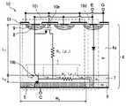
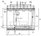
図1は、本発明ではないが基礎とする半導体装置の基本的な構成を説明するための図で、半導体装置10の模式的な断面図である。FIG. 1 is a schematic cross-sectional view of a
図1に示す半導体装置10は、IGBTセルとダイオードセルが、一つの半導体基板4に併設されてなる半導体装置である。図中に一点鎖線で囲った領域10iがIGBTセルに相当し、二点鎖線で囲った領域10dがダイオードセルに相当する。図中には、それぞれの領域に対して、等価回路記号を重ねて示してある。IGBT10iは、MOSトランジスタ10mとバイポーラトランジスタ10bが図のように接続された構成として表され、MOSトランジスタ10mを流れる電流がバイポーラトランジスタ10bのベース電流となる。 A
図1の半導体装置10は、半導体基板4の主面から裏面近くに至るN導電型(N−)の第1半導体層(ボディ層)4aを、IGBTセル10iとダイオードセル10dのキャリアのドリフト層としている。半導体装置10では、半導体基板4の主面側の表層部に、P導電型(P+)の第1半導体領域8が形成され、第1半導体領域8内に、N導電型(N+)の第2半導体領域が形成されている。また、第1半導体領域8と第2半導体領域9に共通接続された共通電極は、IGBTセル10iのエミッタ電極(E)であると共に、ダイオードセル10dのアノード電極にもなっている。尚、図1の半導体装置10における符号G1の部分はゲート酸化膜であり、図1の半導体装置10におけるIGBTセル10iは、平面構造のゲート電極(G)をしている。 The
また、半導体装置10では、半導体基板4の裏面側の表層部に隣接して形成されたP導電型(P+)の第2半導体層5およびN導電型(N+)の第3半導体層6を、それぞれ、IGBTセル10iのコレクタ層およびダイオードセル10dのカソード電極接続層としており、第2半導体層5と第3半導体層6には一体の共通電極(C)が接続している。また、半導体装置10では、第1半導体層4aと第2半導体層5および第3半導体層6との間に、N導電型(N)の第4半導体層7が形成されている。 In the
半導体装置10におけるダイオードセル10dは、第1半導体領域8、第1半導体層4a、第4半導体層7および第3半導体層6で構成され、IGBTセル10iのチャネル形成領域である第1半導体領域8をアノード領域として共用しており、所謂、ボディダイオードセルと呼ばれるものである。尚、図1では、簡単化のために右に図示した第1半導体領域8のみを二点鎖線で囲ってダイオードセル10dと記述しているが、真ん中や左に図示した第1半導体領域8についても、ダイオードセル10dとして機能する。 The
図1に示す半導体装置10は、IGBTセル10iとダイオードセル10dが、一つの半導体基板4に併設されている。また、IGBTセル10iにおいては、キャリアのドリフト層である第1半導体層4aとコレクタ層である第2半導体層5の間に、フィールドストップ(FS)層である第4半導体層7が形成されている。従って、図1の半導体装置10は、図14の半導体装置90と同様に、低オン電圧のFS型IGBTセルとダイオードセルが一つの半導体基板に併設されてなる小型の半導体装置となっている。 In the
一方、図1の半導体装置10は、図14の半導体装置90と類似した構造を有しているが、図14の半導体装置90と異なり、第1半導体層4aと第4半導体層7の厚さと抵抗率および第2半導体層5の基板面内における最小幅に、明確な関係が設定される。すなわち、第1半導体層4aの抵抗率をρ1[Ωcm]、第1半導体層4aの厚さをL1[μm]とし、第4半導体層7の抵抗率をρ2[Ωcm]、第4半導体層7の厚さをL2[μm]とし、第2半導体層5の基板面内における最小幅の1/2をW2[μm]としたとき、図1の半導体装置10では、
(数1) (ρ1/ρ2)×(L1・L2/W22)<1.6
の関係が満たされている。On the other hand, the
(Expression 1) (ρ1 / ρ2 ) × (L1 · L2 / W22 ) <1.6
The relationship is satisfied.
数式1の関係は後述するシミュレーション結果に基づくもので、図1の半導体装置10においては、ρ1,L1,ρ2,L2およびW2が、数式1を満たすように設定されている。これによって、半導体装置10においては、IGBTセル10iにおいて発生するスナップバック電圧VSBを、一般的な使用環境下での最大値である−40℃の閾電圧VCE(th)=0.8Vより小さくすることができる。The relationship of
次に、図1の半導体装置10における数式1の関係が導出された過程を、順を追って説明する。 Next, the process in which the relationship of
最初に、IGBTセルとダイオードセルが併設されてなる半導体装置において、IGBTの電流−電圧特性にスナップバックが発生する理由について、等価回路を用いて説明する。 First, the reason why snapback occurs in the current-voltage characteristics of an IGBT in a semiconductor device in which an IGBT cell and a diode cell are provided together will be described using an equivalent circuit.
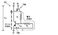
図2は、図1の半導体装置10において、図中に示したIGBTセル10iの等価回路を抜き出した図である。 FIG. 2 is a diagram in which an equivalent circuit of the
図1と図2に示すIGBTセル10iの等価回路では、図14のIGBTセル90iの等価回路では示されていない、抵抗R1が考慮に入れられている。この抵抗R1は、キャリアのドリフト層である第1半導体層(ボディ層)4aの縦方向の抵抗値である。また、図1の半導体装置10では、図中に示した第2半導体層5の基板面内における幅W2が、図14の従来の半導体装置90に較べて、大きく設定される。このため、図1と図2に示すIGBTセル10iの等価回路では、第4半導体層(フィールドストップ層)7の横方向の抵抗R2も考慮に入れられている。In the equivalent circuit of the
最初に、スナップバックについて考察する。 First, consider snapback.
スナップバックとは、図15において、VCEを0Vから増加させた時、ユニポーラモードの動作点A(VCE1,IC1)からバイポーラモードの動作点B(VCE2,IC1)にジャンプする現象であり、VCEの変化量(VCE1−VCE2)がスナップバック電圧VSBである。In FIG. 15, the snapback is a phenomenon in which when VCE is increased from 0 V, a jump from the unipolar mode operating point A (VCE1 , IC1 ) to the bipolar mode operating point B (VCE2 , IC1 ). The change amount of VCE (VCE1 −VCE2 ) is the snapback voltage VSB .
ユニポーラモード(原点〜動作点A)とは、図2の等価回路図において、MOSトランジスタ(MOSFET)10mだけが動作して、図中の細い破線で示した電子の流れのみ存在する動作状態である。この動作状態では、バイポーラトンランジスタ10bはまだ動作しておらず、図中の太い破線で示したホールの流れはない。従って、ボディ層4aの導電率変調は無く、ボディ層4aの抵抗R1、フィールドストップ層7の抵抗R2は、不純物ドーピングによって決まるキャリア濃度で決定された値をとる。このため、ユニポーラモードのI−V特性は、図15に示すように原点を通る直線を呈し、その傾きは1/(R1+R2)で与えられる。The unipolar mode (origin to operating point A) is an operating state in which only the MOS transistor (MOSFET) 10m operates in the equivalent circuit diagram of FIG. 2 and only the electron flow indicated by the thin broken line in the figure exists. . In this operating state, the
図2の等価回路図において、抵抗R2による電圧降下は、バイポーラトランジスタ10bのベース(−エミッタ間)電圧VBEに等しい。図15の動作点A(VCE1,IC1)において、図2の抵抗R2による電圧降下が閾ベース電圧VBE(th)(室温で約0.6V)を越えてバイポーラトンランジスタ10bの動作が始まると、バイポーラトンランジスタ10bのエミッタ層である第2半導体層5から、ホールがフィールドストップ層7を経由してボディ層4aに注入される。このため、ボディ層4aが導電率変調され、その抵抗R1が大幅に低下する。この結果、同じコレクタ電流IC1のもとで、コレクタ電圧がVCE1からVCE2に低下する。すなわち、図15に示したように、動作点Aから動作点Bにジャンプする、いわゆるスナップバックが発生する。In the equivalent circuit diagram of FIG. 2, the voltage drop due to the resistanceR 2, the base of the
図15に示す動作点Bは、I−V特性上においてバイポーラモード上にある点であり、いわゆるIGBTのオン状態、すなわち図2のバイポーラトンランジスタ10bの動作開始点である。また、上記説明からわかるように、図15に示すIGBTの閾電圧VCE(th)は、上記バイポーラトンランジスタ10bの閾ベース電圧VBE(th)に等しい。バイポーラトンランジスタ10bの閾ベース電圧VBE(th)(IGBTの閾電圧VCE(th))は、−40〜150℃の使用環境下では、0.4V程度で、低温ほど高い値となる。室温では、約0.6Vである。The operating point B shown in FIG. 15 is a point in the bipolar mode on the IV characteristic, and is a so-called IGBT on state, that is, an operation starting point of the
次に、スナップバックの抑制条件を考察する。
スナップバックを抑制するためには、スナップバック電圧VSBを小さくすることが必要である。Next, the suppression conditions of snapback are considered.
In order to suppress snapback, it is necessary to reduce the snapback voltageVSB .
スナップバック電圧VSBをR1、R2、VBE(th)で表すと、次の式が得られる。When the snapback voltage VSB is expressed by R1 , R2 , VBE (th) , the following expression is obtained.
図15より、スナップバック電圧VSBは、
(数7) VSB=VCE1−VCE2
である。また、図15の動作点Bにおける図2の分圧関係より、
(数8) VCE1=VBE(th)・(R1+R2)/R2
の関係がある。また、図15に示したように、動作点Bの電圧VCE2は、
(数9) VCE2≒VBE(th)
である。From FIG. 15, the snapback voltage VSB is
(Expression 7) VSB = VCE1 −VCE2
It is. Further, from the partial pressure relationship of FIG. 2 at the operating point B of FIG.
(Number8) V CE1 = V BE ( th) · (
There is a relationship. Also, as shown in FIG. 15, the voltage VCE2 at the operating point B is
(Equation 9) VCE2 ≈ VBE (th)
It is.
次に、数式7〜数式9より、スナップバック電圧VSBが小さい場合には、第1近似で、
(数10) VSB/VBE(th)≒R1/R2
の関係が得られる。Next, from the
(Expression 10) VSB / VBE (th) ≈R1 / R2
The relationship is obtained.
次に、スナップバック電圧VSBをバイポーラトンランジスタ10bの閾ベース電圧VBE(th)より小さくするために、
(数11) VSB/VBE(th)<1
とする。従って数式10により、この場合には、図2の抵抗R1と抵抗R2の間に、
(数12) R1/R2<1
の関係が必要である。Next, in order to make the snapback voltage VSB smaller than the threshold base voltage VBE (th) of the
(Expression 11) VSB / VBE (th) <1
And Thus using
(Equation 12) R1 / R2 <1
Is necessary.
ここで、スナップバック電圧VSBをバイポーラトンランジスタ10bの閾ベース電圧VBE(th)に較べて小さな値とする数式11の関係は、以下に示すように、実際にIGBTを並列動作させる場合においても必要な条件となる。すなわち、スナップバック電圧VSBが大きくなると、IGBT素子を並列接続して動作させた場合に、電流分配がアンバランスになるという不具合が生じる。Here, the relationship of Equation 11 in which the snapback voltage VSB is smaller than the threshold base voltage VBE (th) of the
図3は、上記不具合の内容を説明する図で、図3(a)は、2つのIGBT素子Q1,Q2を並列接続した回路図であり、図3(b)は、図3(a)に示す2つのIGBT素子Q1,Q2のI−V特性を示す図である。FIG. 3 is a diagram for explaining the contents of the above-described problem. FIG. 3A is a circuit diagram in which two IGBT elements Q1 and Q2 are connected in parallel, and FIG. 3B is a circuit diagram of FIG. ) is a diagram showing two the I-V characteristic of the
図3(b)に示すように、2つのIGBT素子Q1,Q2のスナップバック電圧をそれぞれVSB1,VSB2とし、VSB1<VSB2の場合を例にして以下説明する。As shown in FIG. 3B, the snapback voltages of thetwo IGBT elements Q1 and Q2 are VSB1 and VSB2 , respectively, and a case where VSB1 <VSB2 is taken as an example.
VCEが0から増加すると、図3(a)の各IGBT素子Q1,Q2に流れる電流IC1,IC2は、最初は図3(b)に示すラインAに沿ってIC1=IC2で共に増加する。次に、VCEがIGBT素子Q1においてスナップバックが発生する電圧に達すると、各IGBT素子Q1,Q2に流れる電流IC1,IC2は、
(数13) IC1>IC2
となり、アンバランス状態が生じる。When VCE increases from 0, the currents IC1 and IC2 flowing through the IGBT elements Q1 and Q2 in FIG. 3A are initially set to be IC1 = I along the line A shown in FIG. Both increase atC2 .Next, whenV CE reaches the voltage snapback occurs in the IGBT elementQ 1, the currentIC1, I C2 flowing through the
(Equation 13) IC1 > IC2
Thus, an unbalanced state occurs.
さらにVCEが大きくなると、全体のIC(≒IC1)はラインBに沿って増加し、各IGBT素子Q1,Q2に流れる電流IC1,IC2のアンバランスが拡大する。例えば、VCEが電圧aまで増加すると、IGBT素子Q1に流れる電流IC1は電流bとなり、IGBT素子Q2に流れる電流IC2はcとなって、
(数14) b≫c
となる。このアンバランス状態は、VCEがIGBT素子Q2においてスナップバックが発生する電圧に達するまで続く。As VCE further increases, the overall IC (≈IC1 ) increases along the line B, and the imbalance between the currents IC1 and IC2 flowing through the IGBT elements Q1 and Q2 increases. For example, when VCE increases to the voltage a, the current IC1 flowing through the IGBT element Q1 becomes the current b, and the current IC2 flowing through the IGBT element Q2 becomes c,
(Equation 14) b >> c
It becomes. This unbalanced stateis continued until theV CE reaches the voltage snapback occurs in the IGBT elementQ 2.
上記のように、並列接続されたIGBT素子Q1,Q2のようにスナップバック電圧VSBが異なると、並列動作に不具合が生じる。また、たとえ各IGBT素子Q1,Q2のスナップバック電圧VSBを近い値に揃えたとしても、スナップバック電圧VSBに温度依存性があるため、わずかな差で上記不具合が発生してしまう。実際に上記不具合を生じないようにするためには、スナップバック電圧VSBをIGBT素子Q1,Q2のバイポーラトランジスタが動作する時のベース・エミッタ間閾電圧VBE(th)以下とする必要がある。As described above, when the snapback voltage VSB is different as in the case of the IGBT elements Q1 and Q2 connected in parallel, a problem occurs in the parallel operation. Further, even if the snapback voltages VSB of the IGBT elements Q1 and Q2 are made close to each other, the snap back voltage VSB has temperature dependence, and thus the above-described problem occurs with a slight difference. . In order to prevent the above-described problem from actually occurring, the snapback voltage VSB needs to be lower than the base-emitter threshold voltage VBE (th) when the bipolar transistors of the IGBT elements Q1 and Q2 operate. There is.
次に、数式12の関係に戻り、図1に示す半導体装置10のI−V特性をシミュレートするため、抵抗R1,R2を図1に示す構造パラメータ(ρ1,L1,ρ2,L2,W2)を用いて書き換える。何故なら、数式12は図2の集中定数で単純化された等価回路から導かれた式であり、実際の図1に示す半導体装置10の構造から得られる特性は、分布定数であるρ1,ρ2を用いてより正確に表される。例えば、ユニポーラモードにおいて半導体装置10の内部を縦方向に流れる電子は、実際には、図1中に点線矢印iで示したように連続的に分布しており、第4半導体層7に流れ込んだ電子の受ける抵抗は、流れ込む位置によって異なる。このため、正確にI−V特性の評価には、構造パラメータを考慮したデバイスシミュレーションが必要である。Next, returning to the relationship of Formula 12, in order to simulate the IV characteristics of the
図1において、第1半導体層4aの抵抗率をρ1[Ωcm]、第1半導体層4aの厚さをL1[μm]とし、第4半導体層7の抵抗率をρ2[Ωcm]、第4半導体層7の厚さをL2[μm]とし、第2半導体層5の幅をW2[μm]としたとき、
(数15) R1∝ρ1・L1/W2
(数16) R2∝ρ2・L2/W2
の関係が成り立つ。尚、後述するデバイスシミュレーションは、図1の半導体装置10の左端を対称軸として行う。従って、図1に示す第2半導体層5の幅W2は、任意形状の第2半導体層5において基板面内における最小幅の1/2に相当する。In FIG. 1, the resistivity of the
(Equation 15) R1 ∝ρ1 · L1 / W2
(Expression 16) R2 ∝ρ2 · L2 / W2
The relationship holds. Note that device simulation described later is performed with the left end of the
数式15,16を数式12に代入してR1、R2を消去すると、
(数17) af×(ρ1/ρ2)×{L1・L2/W22}<1
の関係が得られる。数式17に導入した因子afは、集中定数であるR1,R2から分布定数であるρ1,ρ2に書き換えたことに伴う形状因子で、1に近い定数である。数式17を書き換えると、
(数18) (ρ1/ρ2)×(L1・L2/W22)<K、 K(=1/af):定数
となり、前述した数式6の関係が導かれる。Substituting Equations 15 and 16 into Equation 12 and erasing R1 and R2 ,
(Expression 17) af × (ρ1 / ρ2 ) × {L1 · L2 / W22 } <1
The relationship is obtained. The factor af introduced into Equation 17 is a shape factor that is associated with rewriting from the concentrated constants R1 and R2 to the distributed constants ρ1 and ρ2 , and is a constant close to 1. When Equation 17 is rewritten,
(Equation 18) (ρ1 / ρ2 ) × (L1 · L2 / W22 ) <K, K (= 1 / af ): Constants are derived, and the relationship of
数式18は、等価回路の考察から導き出したスナップバックの抑制条件であり、上記分析によって、図1の半導体装置10におけるスナップバックの抑制に5個の構造パラメータ(ρ1,L1,ρ2,L2,W2)が関係することがわかった。Equation 18 is a snapback suppression condition derived from the consideration of the equivalent circuit. Based on the above analysis, five structural parameters (ρ1 , L1 , ρ2 , L2 , W2 ) was found to be related.
数式18を用いてスナップバックの発生を抑制した半導体装置10の設計をするにあたって、数式18の右辺のKは、許容するスナップバック電圧VSBに対して定数として取り扱うことができ、このKの値は、構造パラメータ(ρ1,L1,ρ2,L2,W2)の異なる数個のモデルのスナップバック電圧VSBをシミュレートすることで、予め決定しておくことができる。一度Kを定めてしまえば、構造パラメータ(ρ1,L1,ρ2,L2,W2)の異なる任意の半導体装置について、シミュレーションすることなく、許容するスナップバック電圧VSB以下の半導体装置を設計することが可能となる。これによって、設計工数と設計コストを大幅に低減することができる。In designing the
次に、構造パラメータ(ρ1,L1,ρ2,L2,W2)の異なるいくつかのモデルについて、図1に示す半導体装置10の特性をデバイスシミュレートした結果を示す。Next, the results of device simulation of the characteristics of the
図4(a)は、シミュレーションに用いた構造パラメータ(ρ1,L1,ρ2,L2,W2)の代表的な数値を示す図である。FIG. 4A is a diagram illustrating typical numerical values of the structural parameters (ρ1 , L1 , ρ2 , L2 , W2 ) used in the simulation.
5つの構造パラメータ(ρ1,L1,ρ2,L2,W2)のうち、第1半導体層4aに係る構造パラメータρ1,L1はIGBTセルの耐圧に大きな影響を与え、第4半導体層7に関する構造パラメータρ2,L2は、IGBTセルのスイッチング特性に大きな影響を与える。このように、ρ1、L1はIGBTセルの耐圧によりほぼ決定され、ρ2、L2はIGBTセルのスイッチング特性によりほぼ決定されるため、設計自由度は少なく、第2半導体層5の幅W2だけが比較的自由に設計できる。Of the five structural parameters (ρ1 , L1 , ρ2 , L2 , W2 ), the structural parameters ρ1 , L1 related to the
図4(b)には、図1の半導体装置10を自動車用インバータに適用する場合を想定して、車載用において一般的に要求される、600V耐圧と1200V耐圧のIGBTセルとするための構造パラメータ(ρ1、 ρ2、L1、L2)の条件を表にして示した。必要なスイッチング特性を確保すると共に自動車用インバータにおいて一般的に要求される基準の600Vの耐圧を確保するためには、ρ1,ρ2,L1,L2を、ρ1>20[Ωcm]、ρ2<1.0[Ωcm]、L1>40[μm]、L2>0.5[μm]、又は、ρ1>20[Ωcm]、ρ2<1.0[Ωcm]、L1>40[μm]、L2>5.0[μm]とする必要がある。特に、後者の場合には、L2が大きいためρ2を高めに設定することができ、これによって半導体装置10のサージに対する耐性を高めることができる。In FIG. 4B, assuming that the
また、ρ1,ρ2,L1,L2が、ρ1>40[Ωcm]、ρ2<1.0[Ωcm]、L1>80[μm]、L2>0.5[μm]、又は、ρ1>40[Ωcm]、ρ2<1.0[Ωcm]、L1>80[μm]、L2>5.0[μm]である場合には、特に高耐圧の自動車用インバータで要求される基準の1200Vの耐圧を確保することができる。この場合においても、特に後者については、L2が大きいためρ2を高めに設定することができ、これによって半導体装置10のサージに対する耐性を高めることができる。Moreover, ρ1 , ρ2 , L1 , L2 are ρ1 > 40 [Ωcm], ρ2 <1.0 [Ωcm], L1 > 80 [μm], and L2 > 0.5 [μm]. Or ρ1 > 40 [Ωcm], ρ2 <1.0 [Ωcm], L1 > 80 [μm], and L2 > 5.0 [μm], especially for automobiles with a high withstand voltage. A reference voltage of 1200 V required for the inverter can be secured. Also in this case, especially in the latter case, since L2 is large, ρ2 can be set high, and thereby the resistance of the
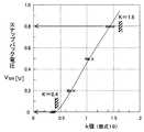
図5は、ρ1=65[Ωcm]、ρ2=0.2[Ωcm]、L1=135[μm]、L2=0.8[μm]、W2=180[μm]とした場合の代表的なI−V特性のシミュレーション結果を示す図である。FIG. 5 shows a case where ρ1 = 65 [Ωcm], ρ2 = 0.2 [Ωcm], L1 = 135 [μm], L2 = 0.8 [μm], and W2 = 180 [μm]. It is a figure which shows the simulation result of typical IV characteristic of.
図5には、バイポーラトランジスタの閾ベース電圧VBE(th)(IGBTの閾電圧VCE(th))が異なる、3つの温度条件でのシミュレーション結果を示した。図中に例示したように、例えば−40℃でのI−V特性から、シミュレーションにより得られるスナップバック電圧VSB=0.5Vを読み取ることができる。FIG. 5 shows simulation results under three temperature conditions in which the threshold base voltage VBE (th) of the bipolar transistor (the threshold voltage VCE (th) of the IGBT) is different. As illustrated in the figure, for example, the snapback voltage VSB = 0.5 V obtained by simulation can be read from the IV characteristic at −40 ° C.
図6(a)は、ρ2とW2をパラメータとして、シミュレーション結果より得られたスナップバック電圧VSBをまとめて示した図である。FIG. 6A is a diagram collectively showing the snapback voltage VSB obtained from the simulation result using ρ2 and W2 as parameters.
また、図6(b)と図6(c)は、それぞれ、図6(a)においてスナップバック電圧VSBが一般的な使用環境下での最大値である−40℃のバイポーラトランジスタの閾ベース電圧VBE(th)(IGBTの閾電圧VCE(th))の0.8Vに等しくなる時、および閾ベース電圧VBE(th)に較べてほぼ無視(0.1Vより小)することができる場合のρ2とW2の組み合わせ、および数式18の左辺である、
(数19) k=(ρ1/ρ2)×(L1・L2/W22)
を計算して、表にした図である。6 (b) and 6 (c) show the threshold base of a bipolar transistor at −40 ° C. in which the snapback voltage VSB in FIG. 6 (a) is the maximum value under a general use environment. When the voltage VBE (th) (the threshold voltage VCE (th) of the IGBT) becomes equal to 0.8V, and is substantially neglected (less than 0.1V) compared to the threshold base voltage VBE (th) A combination of ρ2 and W2 where possible, and the left side of Equation 18.
(Expression 19) k = (ρ1 / ρ2 ) × (L1 · L2 / W22 )
It is the figure which computed and was made into the table | surface.
図6(b)および図6(c)の表からわかるように、許容するスナップバック電圧VSBをバイポーラトランジスタの閾ベース電圧VBE(th)に対して所定の値に設定した時、それを満たす構造パラメータ(ρ1,L1,ρ2,L2,W2)から計算される数式19のk値は、ほぼ一定の値をとる。図6(b)に示すように、VSB〜VBE(th)=0.8Vの場合にはk=1.4〜1.5程度の値であり、図6(c)に示すように、VSB〜0Vの場合はk=0.39程度の値である。As can be seen from the tables of FIG. 6B and FIG. 6C, when the allowable snapback voltage VSB is set to a predetermined value with respect to the threshold base voltage VBE (th) of the bipolar transistor, The k value of Equation 19 calculated from the structural parameters (ρ1 , L1 , ρ2 , L2 , W2 ) to be satisfied is a substantially constant value. As shown in FIG. 6B, when VSB to VBE (th) = 0.8 V, the value is about k = 1.4 to 1.5, and as shown in FIG. In the case of VSB ˜0V, the value is about k = 0.39.
従って、数式18の右辺のKをK=1.6とした、
(数20) (ρ1/ρ2)×(L1・L2/W22)<1.6
を満たす任意の構造パラメータ(ρ1,L1,ρ2,L2,W2)を持った図1に示す半導体装置10は、許容するスナップバック電圧VSBが0.8V以下の半導体装置となる。以上のようにして、先に示した数式1の関係が導出される。Therefore, K on the right side of Equation 18 is set to K = 1.6.
(Expression 20) (ρ1 / ρ2 ) × (L1 · L2 / W22 ) <1.6
The
同様に、数式18の右辺のKをK=0.4とした、
(数21) (ρ1/ρ2)×(L1・L2/W22)<0.4
を満たす任意の構造パラメータ(ρ1,L1,ρ2,L2,W2)を持った図1に示す半導体装置10は、許容するスナップバック電圧VSBをほぼ無視(0.1Vより小)することができる。以上のようにして、先に示した数式2の関係が導出される。Similarly, K on the right side of Equation 18 is set to K = 0.4.
(Formula 21) (ρ1 / ρ2 ) × (L1 · L2 / W22 ) <0.4
The
図7は、上記シミュレーション結果より得られたスナップバック電圧VSBと数式19のk値の関係、およびスナップバック電圧VSBを0.8V以下または0Vとするために設定した数式19のKとの関係をまとめて示した図である。7, and K of the simulation relation k value snapback voltage VSB and formulas 19 obtained from the results, and the snap back voltage VSB formula 19 was set to be less than or 0V 0.8 V the It is the figure which showed the relationship collectively.
前述したように、スナップバックの発生を抑制した図1の半導体装置10の設計をするにあたって、数式19や数式20のように、許容するスナップバック電圧VSBに対して幾つかのシミュレーションモデルによりKの値を定めてしまえば、以後は、構造パラメータ(ρ1,L1,ρ2,L2,W2)の異なる任意の半導体装置について、シミュレーションすることなく、許容するスナップバック電圧VSB以下の半導体装置を設計することが可能となる。これによって、設計工数と設計コストを大幅に低減することができる。As described above, in designing the
また、数式20より、構造パラメータ(ρ1、ρ2、L1、L2)が、例えば図4(b)に示す耐圧600Vの限界値を取った場合には、スナップバック電圧VSB〜VBE(th)=0.8Vとするためには、図1の半導体装置10において、第2半導体層5の基板面内における最小幅の1/2であるW2を、32[μm]より大きくする必要があることがわかる。同様に、耐圧1200Vの限界値を取った場合には、スナップバック電圧VSB〜VBE(th)=0.8Vとするためには、W2を、63[μm]より大きくしなければならない。従って、数式20や数式21を満足する図1に示した半導体装置10は、図14に示した従来の半導体装置90に較べて、IGBTセル10iの幅に相当する第2半導体層5の基板面内における最小幅の1/2であるW2が、大きな半導体装置となる。Further, from the
図1に示した半導体装置10においては、W2を大きくするほど数式20や数式21の関係を満足し易くなるが、W2は、特に、80[μm]以上で500[μm]以下の範囲に設定することが好ましい。W2を80[μm]以上の広い範囲に限定することで、IGBTセル10iとダイオードセル10dの相互干渉を低く抑えて、IGBTセル10iとダイオードセル10dの各特性を安定化させることができる。また、W2を500[μm]以下の狭い範囲に限定することで、基板断面におけるダイオードセル10d(特に図1の左や真ん中に図示した第1半導体領域8をアノード領域とするダイオードセル10d)の電流経路の傾きが抑制されて電流経路長が短くなるため、ダイオードセル10dにおけるスイッチング時の遅延や損失を小さくすることができる。In the
以上のようにして、数式20もしくは数式21を満足する図1に示した半導体装置10は、低オン電圧のFS型IGBTセル10iとダイオードセル10dが一つの半導体基板4に併設されてなる小型の半導体装置であって、スナップバックの発生が抑制された半導体装置とすることができる。また、上述した半導体装置10の設計方法は、設計工数と設計コストを大幅に低減することができる設計方法となっている。 As described above, the
次に、図1の半導体装置10における裏面側の第2半導体層5と第3半導体層6について、基板面内における好適な形状および配置について説明する。 Next, regarding the
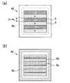
図8(a),(b)は、それぞれ、第2半導体層5と第3半導体層6の好適な形状および配置の例を示す図で、図1の半導体装置10が形成されているチップ20a,20b(半導体基板4)の裏面側を模式的に示した下面図である。また、図8(c)は、図8(a),(b)に示すチップ20a,20bの主面側を模式的に示した上面図である。 8A and 8B are diagrams showing examples of suitable shapes and arrangements of the
図8(c)に示すように、自動車用インバータのように高電圧で利用される図1の半導体装置10の主面側では、一般的に、チップ20a,20bの中央部に、IGBTセル10iとダイオードセル10dで共用する第1半導体領域8が形成されたセル領域Rcが配置される。また、チップ20a,20bの外周部には、ガードリング等が形成された高電圧領域Rbが配置される。 As shown in FIG. 8 (c), on the main surface side of the
本発明に係る半導体装置では、図8(a),(b)に示すように、チップ20a,20bの裏面側では、第2半導体層5と第3半導体層6が、点線で示した主面側の外周部に配置される高電圧領域Rbより内側に配置されている。これによって、例えば第2半導体層5を中央部に配置して第3半導体層6を主面側の外周部に配置されている高電圧領域Rbの直下に配置する場合に較べて、先に説明したW2を500[μm]以下の狭い範囲に限定する場合と同様に、基板断面におけるダイオードセル10dの電流経路の傾きが抑制されて電流経路長が短くなる。このため、ダイオードセ10dにおけるスイッチング時の遅延や損失を小さくすることができる。In the semiconductor device according to the present invention, as shown in FIGS. 8A and 8B, the
また、図8(a),(b)に示すチップ20a,20bでは、第2半導体層5と第3半導体層6の基板面内における形状が短冊形状であり、第2半導体層5と第3半導体層6が基板面内において交互に配置されている。この場合、図8(a)に示すように、図1の半導体装置10におけるW2の2倍が、第2半導体層5の最小幅に相当している。また、図8(b)に示すチップ20bでは、特に、第2半導体層5と第3半導体層6が交互に配置された領域の両端が、第2半導体層5a,5bで構成されている。Further, in the
第2半導体層5と第3半導体層6の形状と配置については、第2半導体層5を円形状として基板面内において等間隔に配置し、それらを取り囲むように第3半導体層6を配置する構成としてもよい。しかしながら、第2半導体層5と第3半導体層6を図8(a),(b)に示すように短冊形状として交互配置することで、IGBTセル10iとダイオードセル10dで共用する第1半導体領域8の配置密度を高め、基板を有効利用することができる。また、図8(b)に示すように、第2半導体層5と第3半導体層6が交互に配置された領域の両端を第2半導体層5a,5bで構成することで、ダイオードセル10dにおけるスイッチング時の遅延や損失を小さくすることができる。尚、図8(a),(b)では上記第2半導体層5と第3半導体層6の配置関係を理解し易くするためにチップ20a,20bの外周部における半導体層の分類が記載されていないが、チップ20a,20bの外周部を第2半導体層5として、第2半導体層5中に短冊形状の第3半導体層6が等間隔に配置された構成とすることが好ましい。 About the shape and arrangement | positioning of the
図9は、本発明に係る半導体装置の例で、半導体装置30の模式的な断面図である。尚、図9の半導体装置30において、図1の半導体装置10と同様の部分については、同じ符号を付した。Figure 9 shows an example of a semiconductor deviceaccording to the present invention, is a schematic sectional view of the
図1の半導体装置10におけるダイオードセル10dは、IGBTセル10iのチャネル形成領域である第1半導体領域8をアノード領域として共用しており、所謂、ボディダイオードセルだけで構成されていた。一方、図9に示す半導体装置30は、IGBTセル10iとボディダイオードセル10dに追加して、図中に破線で囲った以下に示す独立ダイオードセル30dを有している。すなわち、図9の半導体装置30においては、半導体基板4の主面側の表層部に、第1半導体領域8と分離して、P導電型(P+)の第3半導体領域8aが形成されている。また、第3半導体領域8aに接続する電極が、第1半導体領域8と第2半導体領域9に接続する共通電極(E)に接続されている。これによって、第3半導体領域8a、第1半導体層4a、第4半導体層7および第3半導体層7からなる、独立ダイオードセル30dが形成されている。 The
図9の半導体装置30においては、IGBTセル10iとの関係でボディダイオードセル10dだけでは電流容量が確保できない場合であっても、独立ダイオードセル30dを併設することによって電流容量の不足分を補うことができ、大きな電流容量を確保することができる。尚、独立ダイオードセル30dの第3半導体領域8aは、IGBTセル10dから離れた位置に形成できると共に不純物濃度を適宜設定することができ、これによって独立ダイオードセルの形成に伴うIGBTセル10iのリカバリー特性の悪化を抑制することができる。 In the
尚、図9に示した半導体装置30についても、構造パラメータ(ρ1、ρ2、L1、L2、W2)が数式20もしくは数式21を満足するように設定される。従って、図9の半導体装置30も、低オン電圧のFS型IGBTセル10iとダイオードセル10d,30dが一つの半導体基板4に併設されてなる小型の半導体装置であって、スナップバックの発生が抑制された半導体装置とすることができる。Also for the
次に、図9の半導体装置30における裏面側の第2半導体層5と第3半導体層6および主面側の第1半導体領域8と第3半導体領域8aについて、基板面内における好適な形状および配置について説明する。 Next, for the
図10(a),(b)は、図9の半導体装置30が形成されているチップ40(半導体基板4)を模式的に示した図で、図10(a)は、裏面側の第2半導体層5と第3半導体層6の好適な形状および配置の例を示した下面図で、図10(b)は、主面側の第1半導体領域8と第3半導体領域8aの好適な形状および配置の例を示した上面図である。尚、図10に示すチップ40において、図8に示すチップ20a,20bと同様の部分については、同じ符号を付した。 FIGS. 10A and 10B are diagrams schematically showing a chip 40 (semiconductor substrate 4) on which the
図10(a)に示すように、チップ40の裏面側における第2半導体層5と第3半導体層6の形状および配置は、図8(a)に示すチップ20aの裏面側における第2半導体層5と第3半導体層6の形状および配置と同じである。一方、図10(b)に示すように、チップ40の主面側におけるIGBTセル10iとダイオードセル10dで共用する第1半導体領域8が形成されたセル領域Rcは、短冊形状(短冊形状の第1半導体領域8が平行に配置されている)である。また、短冊形状のセル領域Rcに対して、同じ短冊形状(短冊形状の第3半導体領域8aが平行に配置されている)の独立ダイオードセル領域Rdが、交互に配置された構成となっている。図10(a),(b)に示すチップ40においては、第1半導体領域8からなるセル領域Rcが、第2半導体層2の直上に配置され、第3半導体領域8aからなる独立ダイオードセル領域Rdが、第3半導体層6の直上に配置されている。これによって、独立ダイオードセル領域Rd内にある独立ダイオードセル30dについて、スイッチング時の遅延や損失を小さくすることができる。尚、図10(a),(b)では、第2半導体層5(セル領域Rc)と第3半導体層6(独立ダイオードセル領域Rd)がほぼ等しい幅の短冊形状となっているが、短冊形状の第2半導体層5(セル領域Rc)と第3半導体層6(独立ダイオードセル領域Rd)の各幅は、IGBTセル10iとダイオードセル10dおよび独立ダイオードセル30dのそれぞれの要求特性によって、適宜設定される。また、図10(a)においても上記第2半導体層5と第3半導体層6の配置関係を理解し易くするためにチップ40の外周部における半導体層の分類が記載されていないが、チップ40の外周部を第2半導体層5として、第2半導体層5中に短冊形状の第3半導体層6が等間隔に配置された構成とすることが好ましい。 As shown in FIG. 10A, the shape and arrangement of the
図11と図12は、別の半導体装置の例で、それぞれ、本発明ではないが基礎とする半導体装置50と本発明に係る半導体装置60の模式的な断面図である。尚、図11と図12の半導体装置50,60において、図1と図9の半導体装置10,30と同様の部分については、同じ符号を付した。FIG. 11 and FIG. 12 are examples ofother semiconductor devicesand are schematic cross-sectional views of a semiconductor device 50basedon the
図1と図9の半導体装置10,30では、いずれも、平面構造のゲート電極(G)を有するIGBTセル10iが形成されていた。これに対して、図11と図12に示す半導体装置50,60においては、側壁酸化膜G2と埋め込み多結晶シリコンG3からなるトレンチ構造のゲート電極(G)を有するIGBTセル50iが形成されている。半導体装置50,60では、半導体基板4の主面側の表層部に連続する第1半導体領域8aが形成されており、第1半導体領域8aを共用して、IGBTセル50iとボディダイオードセル50dが構成されている。尚、図11の半導体装置50は、IGBTセル50iとボディダイオードセル50dだけで構成されている。一方、図12の半導体装置60では、独立ダイオードセル30dが追加形成されている。 In each of the
尚、図11と図12に示した半導体装置50,60についても、構造パラメータ(ρ1、ρ2、L1、L2、W2)が数式20もしくは数式21を満足するように設定される。従って、図11と図12の半導体装置50,60も、低オン電圧のFS型IGBTセル50iとダイオードセル50d,30dが一つの半導体基板4に併設されてなる小型の半導体装置であって、スナップバックの発生が抑制された半導体装置とすることができる。Note that the structural parameters (ρ1 , ρ2 , L1 , L2 , W2 ) of the
尚、図1に示した半導体装置10は、N導電型半導体基板4の裏面側に、P導電型のIGBTセル10iのコレクタ層5とダイオードセル10dのN導電型のカソード電極接続層6が形成された半導体装置である。半導体装置の構成要素であるIGBTに関して良好な特性を得るためには、図1に示した半導体装置10の各部の導電型構成が好ましいが、半導体装置10における各領域の導電型を全て逆転した半導体装置であってもよい。すなわち、P導電型半導体基板の裏面側に、N導電型のIGBTセルのコレクタ層とP導電型のダイオードセルのアノード電極接続層が形成された半導体装置についても、上述した半導体装置10に対する効果の説明が同様に適用できることは言うまでもない。従って、上記半導体装置10における各領域の導電型を全て逆転した半導体装置も、低オン電圧のFS型IGBTセルとダイオードセルが一つの半導体基板に併設されてなる小型の半導体装置であって、スナップバックの発生が抑制された半導体装置とすることができる。In the
図13に、図1の半導体装置10における各領域の導電型を全て逆転した半導体装置70を示す。 FIG. 13 shows a
以上に示した半導体装置は、いずれも、IGBTセルとダイオードセルおよび独立ダイオードセルが一つの半導体基板に併設されてなる小型の半導体装置である。従って、上記半導体装置は、IGBTとフリーホイールダイオード(FWD)の組み合わせで構成されるインバータ回路に用いられる半導体装置であって、前記ダイオードセルおよび独立ダイオードセルからなるダイオードが、前記FWDとして用いられる場合に好適である。 Each of the semiconductor devices described above is a small semiconductor device in which an IGBT cell, a diode cell, and an independent diode cell are provided on one semiconductor substrate. Therefore, the semiconductor device is a semiconductor device used in an inverter circuit composed of a combination of an IGBT and a free wheel diode (FWD), and the diode composed of the diode cell and the independent diode cell is used as the FWD. It is suitable for.
また、上記半導体装置は、小型の半導体装置であって、前述したように厳しい使用環境下においてもスナップバック電圧VSBを抑制することができ、高耐圧も確保することができる。従って、上記半導体装置は、車載用の半導体装置として好適である。Further, the semiconductor device is a small semiconductor device, and can suppress the snapback voltageVSB even under a severe use environment as described above, and can secure a high breakdown voltage. Therefore, the semiconductor device is suitable as a vehicle-mounted semiconductor device.
10,30,50,60,70,90 半導体装置
10i,50i,90i IGBT(セル)
10m MOSトランジスタ
10b バイポーラトランジスタ
10d,50d,90d (ボディ)ダイオード(セル)
30d 独立ダイオードセル
4 半導体基板
4a 第1半導体層(ボディ層、キャリアのドリフト層)
5 第2半導体層(IGBTセル10iのコレクタ層)
6 第3半導体層(ダイオードセル10dのカソード電極接続層)
7 第4半導体層(フィールドストップ層、FS層)
8,8b 第1半導体領域
8a 第3半導体領域
9 第2半導体領域10, 30, 50, 60, 70, 90
30d
5 Second semiconductor layer (collector layer of
6 Third semiconductor layer (cathode electrode connection layer of
7 Fourth semiconductor layer (field stop layer, FS layer)
8, 8b
Claims (13)
Translated fromJapanese前記半導体基板の主面から裏面近くに至る第1導電型の第1半導体層を、前記IGBTセルとダイオードセルのキャリアのドリフト層とし、
前記半導体基板の裏面側の表層部に同じ厚さで隣接して形成された第2導電型の第2半導体層および第1導電型の第3半導体層を、それぞれ、前記IGBTセルのコレクタ層および前記ダイオードセルの一方の電極接続層とし、
前記第2半導体層と第3半導体層の基板面内における形状が、短冊形状であり、
前記第3半導体層が、前記半導体基板の裏面側において、
当該半導体基板の主面側の外周部に配置される高電圧領域より内側に配置されてなり、
前記第1半導体層と前記第2半導体層および第3半導体層との間に、第1導電型の第4半導体層が形成されてなり、
前記第1半導体層の抵抗率をρ1[Ωcm]、第1半導体層の厚さをL1[μm]とし、前記第4半導体層の抵抗率をρ2[Ωcm]、第4半導体層の厚さをL2[μm]とし、前記第2半導体層の基板面内における最小幅の1/2をW2[μm]としたとき、
(数1) (ρ1/ρ2)×(L1・L2/W22)<1.6
の関係にあり、
前記半導体基板の主面側の表層部に、第2導電型の第1半導体領域が形成され、
前記第1半導体領域内に、第1導電型の第2半導体領域が形成され、
前記第1半導体領域と第2半導体領域に共通接続された共通電極を、前記IGBTセルのエミッタ電極および前記ダイオードセルのもう一方の電極とし、
前記半導体基板の主面側の表層部に、前記第1半導体領域と分離して、第2導電型の第3半導体領域が形成され、
前記第3半導体領域に接続する電極が、前記共通電極に接続されてなり、
前記第3半導体領域、第1半導体層、第4半導体層および第3半導体層で、独立ダイオードセルが形成されてなることを特徴とする半導体装置。A semiconductor device in which an IGBT cell and a diode cell are provided on a single semiconductor substrate,
The first conductivity type first semiconductor layer extending from the main surface of the semiconductor substrate to the vicinity of the back surface is used as a carrier drift layer of the IGBT cell and the diode cell,
The second conductivity type second semiconductor layer and the first conductivity type third semiconductor layer formed adjacent to the surface layer portion on the back surface side of the semiconductor substrate with thesame thickness are respectively connected to the collector layer of the IGBT cell and As one electrode connection layer of the diode cell,
The shape of the second semiconductor layer and the third semiconductor layer in the substrate plane is a strip shape,
The third semiconductor layer is on the back side of the semiconductor substrate,
It is arranged inside the high voltage region arranged in the outer peripheral part on the main surface side of the semiconductor substrate,
A fourth semiconductor layer of a first conductivity type is formed between the first semiconductor layer and the second and third semiconductor layers;
The resistivity of the first semiconductor layer is ρ1 [Ωcm], the thickness of the first semiconductor layer is L1 [μm], the resistivity of the fourth semiconductor layer is ρ2 [Ωcm], When the thickness is L2 [μm] and ½ of the minimum width in the substrate surface of the second semiconductor layer is W2 [μm],
(Expression 1) (ρ1 / ρ2 ) × (L1 · L2 / W22 ) <1.6
Near the relationshipis,
A first semiconductor region of a second conductivity type is formed in a surface layer portion on a main surface side of the semiconductor substrate;
A second semiconductor region of a first conductivity type is formed in the first semiconductor region;
A common electrode commonly connected to the first semiconductor region and the second semiconductor region as an emitter electrode of the IGBT cell and another electrode of the diode cell;
A third semiconductor region of a second conductivity type is formed in a surface layer portion on the main surface side of the semiconductor substrate, separated from the first semiconductor region,
An electrode connected to the third semiconductor region is connected to the common electrode;
Said third semiconductor region, the first semiconductor layer, the fourth semiconductor layer and the third semiconductor layer, and wherein aa is independently diode cell is formed Rukoto.
(数2) (ρ1/ρ2)×(L1・L2/W22)<0.4
であることを特徴とする請求項1に記載の半導体装置。In the semiconductor device,
(Expression 2) (ρ1 / ρ2 ) × (L1 · L2 / W22 ) <0.4
The semiconductor device according to claim 1, wherein:
(数3) ρ1>20、 ρ2<1.0、 L1>40、 L2>0.5
であることを特徴とする請求項1または2に記載の半導体装置。Said ρ1 , ρ2 , L1 , L2 are
(Equation 3) ρ1 > 20, ρ2 <1.0, L1 > 40, L2 > 0.5
The semiconductor device according to claim 1, wherein:
(数4) ρ1>40、 ρ2<1.0、 L1>80、 L2>0.5
であることを特徴とする請求項3に記載の半導体装置。Said ρ1 , ρ2 , L1 , L2 are
(Equation 4) ρ1 > 40, ρ2 <1.0, L1 > 80, L2 > 0.5
The semiconductor device according to claim 3, wherein:
(数5) L2>5.0
であることを特徴とする請求項3または4に記載の半導体装置。L2 is
(Equation 5) L2 > 5.0
The semiconductor device according to claim 3, wherein the semiconductor device is a semiconductor device.
前記第1半導体領域と第3半導体領域が、基板面内において、交互に配置されてなることを特徴とする請求項7または8に記載の半導体装置。The shape of the first semiconductor region and the third semiconductor region in the substrate plane is a strip shape,
9. The semiconductor device according to claim7,wherein the first semiconductor region and the third semiconductor region are alternately arranged in the substrate surface .
前記第3半導体領域が、基板面内において、前記第3半導体層の直上に配置されてなることを特徴とする請求項9に記載の半導体装置。The first semiconductor region is disposed immediately above the second semiconductor layer in a substrate plane;
The semiconductor device according to claim 9,wherein the third semiconductor region is disposed immediately above the third semiconductor layer in a substrate plane .
前記ダイオードセルおよび独立ダイオードセルからなるダイオードが、フリーホイールダイオードとして用いられることを特徴とする請求項1乃至11のいずれか一項に記載の半導体装置。The semiconductor device is a semiconductor device used for an inverter circuit,
The semiconductor device according toany one of claims1 to 11wherein the diode cell and an independent diode cell diode, characterized in thatit is used as a freewheeling diode.
Priority Applications (5)
| Application Number | Priority Date | Filing Date | Title |
|---|---|---|---|
| JP2007060809AJP5157201B2 (en) | 2006-03-22 | 2007-03-09 | Semiconductor device |
| DE112007000010TDE112007000010B4 (en) | 2006-03-22 | 2007-03-20 | Semiconductor device with IGBT cell and diode cell, and method for designing thereof |
| CN2007800004744ACN101322248B (en) | 2006-03-22 | 2007-03-20 | Semiconductor device with IGBT unit and diode unit and design method thereof |
| PCT/JP2007/055600WO2007108456A1 (en) | 2006-03-22 | 2007-03-20 | Semiconductor device having igbt cells and diode cells, and its designing method |
| US11/885,334US7692214B2 (en) | 2006-03-22 | 2007-03-20 | Semiconductor device having IGBT cell and diode cell and method for designing the same |
Applications Claiming Priority (3)
| Application Number | Priority Date | Filing Date | Title |
|---|---|---|---|
| JP2006079153 | 2006-03-22 | ||
| JP2006079153 | 2006-03-22 | ||
| JP2007060809AJP5157201B2 (en) | 2006-03-22 | 2007-03-09 | Semiconductor device |
Publications (2)
| Publication Number | Publication Date |
|---|---|
| JP2007288158A JP2007288158A (en) | 2007-11-01 |
| JP5157201B2true JP5157201B2 (en) | 2013-03-06 |
Family
ID=38522484
Family Applications (1)
| Application Number | Title | Priority Date | Filing Date |
|---|---|---|---|
| JP2007060809AActiveJP5157201B2 (en) | 2006-03-22 | 2007-03-09 | Semiconductor device |
Country Status (5)
| Country | Link |
|---|---|
| US (1) | US7692214B2 (en) |
| JP (1) | JP5157201B2 (en) |
| CN (1) | CN101322248B (en) |
| DE (1) | DE112007000010B4 (en) |
| WO (1) | WO2007108456A1 (en) |
Families Citing this family (58)
| Publication number | Priority date | Publication date | Assignee | Title |
|---|---|---|---|---|
| JP5103830B2 (en)* | 2006-08-28 | 2012-12-19 | 三菱電機株式会社 | Insulated gate semiconductor device |
| ITTO20080045A1 (en) | 2008-01-18 | 2009-07-19 | St Microelectronics Srl | PLACE OF PHOTODIODS OPERATING IN GEIGER MODES MUTUALLY INSULATED AND RELATIVE PROCESS OF MANUFACTURING |
| ITTO20080046A1 (en) | 2008-01-18 | 2009-07-19 | St Microelectronics Srl | PLACE OF PHOTODIODS OPERATING IN GEIGER MODES MUTUALLY INSULATED AND RELATIVE PROCESS OF MANUFACTURING |
| JP5206541B2 (en)* | 2008-04-01 | 2013-06-12 | 株式会社デンソー | Semiconductor device and manufacturing method thereof |
| EP2184781A1 (en)* | 2008-11-05 | 2010-05-12 | ABB Technology AG | Reverse-conducting semiconductor device |
| JP5963385B2 (en)* | 2008-11-26 | 2016-08-03 | 富士電機株式会社 | Semiconductor device |
| US8507352B2 (en)* | 2008-12-10 | 2013-08-13 | Denso Corporation | Method of manufacturing semiconductor device including insulated gate bipolar transistor and diode |
| JP4947111B2 (en)* | 2008-12-10 | 2012-06-06 | 株式会社デンソー | Manufacturing method of semiconductor device |
| IT1392366B1 (en)* | 2008-12-17 | 2012-02-28 | St Microelectronics Rousset | OPERATING PHOTODIODO IN GEIGER MODE WITH INTEGRATED AND CONTROLLABLE SUPPRESSION RESISTOR, PHOTODIUM RING AND RELATIVE PROCESS OF PROCESSING |
| JP5045733B2 (en)* | 2008-12-24 | 2012-10-10 | 株式会社デンソー | Semiconductor device |
| JP4905559B2 (en)* | 2009-01-27 | 2012-03-28 | 株式会社デンソー | Semiconductor device |
| JP4877337B2 (en) | 2009-02-17 | 2012-02-15 | トヨタ自動車株式会社 | Semiconductor device |
| JP4929304B2 (en)* | 2009-03-13 | 2012-05-09 | 株式会社東芝 | Semiconductor device |
| IT1393781B1 (en) | 2009-04-23 | 2012-05-08 | St Microelectronics Rousset | OPERATING PHOTODIODO IN GEIGER MODE WITH INTEGRATED AND CONTROLLABLE JFET EFFECT SUPPRESSION RESISTOR, PHOTODIUM RING AND ITS PROCESS OF PROCESSING |
| EP2249392B1 (en)* | 2009-04-29 | 2020-05-20 | ABB Power Grids Switzerland AG | Reverse-conducting semiconductor device |
| JP2011023527A (en)* | 2009-07-15 | 2011-02-03 | Toshiba Corp | Semiconductor device |
| CN102013422B (en)* | 2009-09-07 | 2012-08-22 | 比亚迪股份有限公司 | Insulated gate bipolar translator power tube module |
| CN102714218B (en)* | 2009-11-10 | 2015-09-30 | Abb技术有限公司 | Punch-through semiconductor device and production method thereof |
| JP5182766B2 (en)* | 2009-12-16 | 2013-04-17 | 三菱電機株式会社 | High voltage semiconductor device |
| JP5587622B2 (en) | 2010-01-27 | 2014-09-10 | ルネサスエレクトロニクス株式会社 | Reverse conduction type IGBT |
| IT1399690B1 (en) | 2010-03-30 | 2013-04-26 | St Microelectronics Srl | AVALANCHE PHOTODIODO OPERATING IN GEIGER MODE WITH HIGH SIGNAL NOISE REPORT AND RELATIVE MANUFACTURING PROCEDURE |
| KR101276407B1 (en) | 2010-05-07 | 2013-06-19 | 도요타지도샤가부시키가이샤 | Semiconductor device |
| JP5678469B2 (en)* | 2010-05-07 | 2015-03-04 | 株式会社デンソー | Semiconductor device |
| JP5582102B2 (en)* | 2010-07-01 | 2014-09-03 | 株式会社デンソー | Semiconductor device |
| US8716746B2 (en) | 2010-08-17 | 2014-05-06 | Denso Corporation | Semiconductor device |
| WO2012036247A1 (en)* | 2010-09-17 | 2012-03-22 | 富士電機株式会社 | Semiconductor device |
| JP5321669B2 (en) | 2010-11-25 | 2013-10-23 | 株式会社デンソー | Semiconductor device |
| US8482029B2 (en)* | 2011-05-27 | 2013-07-09 | Infineon Technologies Austria Ag | Semiconductor device and integrated circuit including the semiconductor device |
| JP5737102B2 (en)* | 2011-09-19 | 2015-06-17 | 株式会社デンソー | Semiconductor device |
| JP5200148B2 (en)* | 2011-10-07 | 2013-05-15 | トヨタ自動車株式会社 | Semiconductor device |
| JP5742711B2 (en)* | 2011-12-28 | 2015-07-01 | 株式会社デンソー | Semiconductor device |
| JP6022774B2 (en) | 2012-01-24 | 2016-11-09 | トヨタ自動車株式会社 | Semiconductor device |
| JP2013235891A (en)* | 2012-05-07 | 2013-11-21 | Denso Corp | Semiconductor device |
| JP5619079B2 (en)* | 2012-06-15 | 2014-11-05 | 三菱電機株式会社 | High voltage semiconductor device |
| JP2014022708A (en)* | 2012-07-17 | 2014-02-03 | Yoshitaka Sugawara | Semiconductor device and operation method of the same |
| WO2014041652A1 (en)* | 2012-09-13 | 2014-03-20 | 富士電機株式会社 | Semiconductor device and method for manufacturing semiconductor device |
| US9070571B2 (en)* | 2013-03-15 | 2015-06-30 | Infineon Technologies Ag | Power switching module with reduced oscillation |
| JP5949646B2 (en) | 2013-04-10 | 2016-07-13 | 株式会社デンソー | Semiconductor device |
| CN103383957B (en)* | 2013-07-08 | 2015-08-19 | 电子科技大学 | A kind of inverse conductivity type IGBT device |
| JP6225649B2 (en)* | 2013-11-12 | 2017-11-08 | 株式会社デンソー | Insulated gate bipolar transistor and manufacturing method thereof |
| JP6383971B2 (en)* | 2013-12-27 | 2018-09-05 | 良孝 菅原 | Semiconductor device |
| JP2015207588A (en)* | 2014-04-17 | 2015-11-19 | ローム株式会社 | Semiconductor device |
| JP6181597B2 (en) | 2014-04-28 | 2017-08-16 | トヨタ自動車株式会社 | Semiconductor device and manufacturing method of semiconductor device |
| JP6908528B2 (en) | 2015-12-11 | 2021-07-28 | ローム株式会社 | Semiconductor device |
| JP2017118060A (en) | 2015-12-25 | 2017-06-29 | ローム株式会社 | Semiconductor device and semiconductor device manufacturing method |
| JP6723784B2 (en) | 2016-03-28 | 2020-07-15 | ローム株式会社 | diode |
| JP2017208413A (en) | 2016-05-17 | 2017-11-24 | 株式会社デンソー | Semiconductor device |
| CN106098764B (en)* | 2016-07-26 | 2019-05-14 | 电子科技大学 | A kind of binary channels RC-LIGBT device and preparation method thereof |
| CN106098763B (en)* | 2016-07-26 | 2019-05-10 | 电子科技大学 | A kind of RC-LIGBT device and preparation method thereof |
| CN106098762B (en)* | 2016-07-26 | 2019-05-14 | 电子科技大学 | A kind of RC-IGBT device and preparation method thereof |
| CN106129110B (en)* | 2016-07-26 | 2019-05-10 | 电子科技大学 | A dual-channel RC-IGBT device and preparation method thereof |
| US10892319B2 (en)* | 2016-08-19 | 2021-01-12 | Rohm Co., Ltd. | Semiconductor device |
| JP6935731B2 (en) | 2017-11-16 | 2021-09-15 | 株式会社デンソー | Semiconductor device |
| JP7131632B2 (en)* | 2018-12-19 | 2022-09-06 | 三菱電機株式会社 | semiconductor equipment |
| CN111697067B (en)* | 2019-03-15 | 2023-11-24 | 上海睿驱微电子科技有限公司 | Reverse conducting insulated gate bipolar transistor capable of rapid snapback and implementation method thereof |
| JP2020129675A (en)* | 2020-04-21 | 2020-08-27 | ローム株式会社 | Semiconductor device |
| CN112466935B (en)* | 2020-12-15 | 2023-03-14 | 重庆邮电大学 | RC-IGBT device with polycrystalline silicon electronic channel of collector electrode |
| CN114759078B (en)* | 2022-03-28 | 2024-08-30 | 重庆大学 | A reverse conducting insulated gate bipolar transistor |
Family Cites Families (7)
| Publication number | Priority date | Publication date | Assignee | Title |
|---|---|---|---|---|
| JPH053205A (en)* | 1991-01-25 | 1993-01-08 | Fuji Electric Co Ltd | Insulated gate bipolar transistor |
| JPH06196705A (en)* | 1992-12-24 | 1994-07-15 | Hitachi Ltd | Reverse conduction type insulated gate bipolar transistor and manufacturing method thereof |
| JP3951868B2 (en)* | 2002-09-12 | 2007-08-01 | 富士電機デバイステクノロジー株式会社 | Semiconductor device and manufacturing method thereof |
| DE10250575B4 (en)* | 2002-10-30 | 2010-04-15 | Infineon Technologies Ag | IGBT with monolithically integrated antiparallel diode |
| JP4403366B2 (en)* | 2003-06-04 | 2010-01-27 | 富士電機デバイステクノロジー株式会社 | Semiconductor device and manufacturing method thereof |
| JP2005057235A (en) | 2003-07-24 | 2005-03-03 | Mitsubishi Electric Corp | Insulated gate bipolar transistor, method of manufacturing the same, and inverter circuit |
| JP2005354031A (en)* | 2004-05-13 | 2005-12-22 | Mitsubishi Electric Corp | Semiconductor device |
- 2007
- 2007-03-09JPJP2007060809Apatent/JP5157201B2/enactiveActive
- 2007-03-20DEDE112007000010Tpatent/DE112007000010B4/ennot_activeExpired - Fee Related
- 2007-03-20USUS11/885,334patent/US7692214B2/enactiveActive
- 2007-03-20CNCN2007800004744Apatent/CN101322248B/ennot_activeExpired - Fee Related
- 2007-03-20WOPCT/JP2007/055600patent/WO2007108456A1/enactiveApplication Filing
Also Published As
| Publication number | Publication date |
|---|---|
| WO2007108456A1 (en) | 2007-09-27 |
| US20080315248A1 (en) | 2008-12-25 |
| DE112007000010T5 (en) | 2008-02-14 |
| JP2007288158A (en) | 2007-11-01 |
| CN101322248B (en) | 2010-09-29 |
| US7692214B2 (en) | 2010-04-06 |
| CN101322248A (en) | 2008-12-10 |
| DE112007000010B4 (en) | 2013-02-07 |
Similar Documents
| Publication | Publication Date | Title |
|---|---|---|
| JP5157201B2 (en) | Semiconductor device | |
| JP5742711B2 (en) | Semiconductor device | |
| JP5034461B2 (en) | Semiconductor device | |
| US6693327B2 (en) | Lateral semiconductor component in thin-film SOI technology | |
| US9153575B2 (en) | Semiconductor device | |
| CN107148675B (en) | Semiconductor device with a plurality of semiconductor chips | |
| JP5737102B2 (en) | Semiconductor device | |
| US7989885B2 (en) | Semiconductor device having means for diverting short circuit current arranged in trench and method for producing same | |
| US8916931B2 (en) | LDMOS semiconductor device with parasitic bipolar transistor for reduced surge current | |
| JP2009152506A (en) | Semiconductor device | |
| CN104871312A (en) | Semiconductor device | |
| US20140070271A1 (en) | Lateral insulated gate bipolar transistor | |
| JP2009188178A (en) | Semiconductor device | |
| JP5235443B2 (en) | Trench gate type semiconductor device | |
| US8766317B2 (en) | Semiconductor device | |
| JP2019161079A (en) | Silicon carbide semiconductor device and silicon carbide semiconductor circuit device | |
| JP6299658B2 (en) | Insulated gate type switching element | |
| JP6088401B2 (en) | Reverse conducting IGBT | |
| US9099521B2 (en) | Reverse conducting IGBT | |
| JP2008027945A (en) | Trench type insulated gate bipolar transistor | |
| JPWO2019012813A1 (en) | Semiconductor device | |
| US11004964B2 (en) | Semiconductor device | |
| JP4910489B2 (en) | Insulated gate bipolar transistor | |
| JP4821086B2 (en) | Semiconductor device | |
| US7319263B2 (en) | Semiconductor component with switching element configured to reduce parasitic current flow |
Legal Events
| Date | Code | Title | Description |
|---|---|---|---|
| A621 | Written request for application examination | Free format text:JAPANESE INTERMEDIATE CODE: A621 Effective date:20090629 | |
| A131 | Notification of reasons for refusal | Free format text:JAPANESE INTERMEDIATE CODE: A131 Effective date:20120529 | |
| A521 | Request for written amendment filed | Free format text:JAPANESE INTERMEDIATE CODE: A523 Effective date:20120716 | |
| A131 | Notification of reasons for refusal | Free format text:JAPANESE INTERMEDIATE CODE: A131 Effective date:20120828 | |
| A521 | Request for written amendment filed | Free format text:JAPANESE INTERMEDIATE CODE: A523 Effective date:20121025 | |
| TRDD | Decision of grant or rejection written | ||
| A01 | Written decision to grant a patent or to grant a registration (utility model) | Free format text:JAPANESE INTERMEDIATE CODE: A01 Effective date:20121113 | |
| A61 | First payment of annual fees (during grant procedure) | Free format text:JAPANESE INTERMEDIATE CODE: A61 Effective date:20121126 | |
| R151 | Written notification of patent or utility model registration | Ref document number:5157201 Country of ref document:JP Free format text:JAPANESE INTERMEDIATE CODE: R151 | |
| FPAY | Renewal fee payment (event date is renewal date of database) | Free format text:PAYMENT UNTIL: 20151221 Year of fee payment:3 | |
| R250 | Receipt of annual fees | Free format text:JAPANESE INTERMEDIATE CODE: R250 | |
| R250 | Receipt of annual fees | Free format text:JAPANESE INTERMEDIATE CODE: R250 | |
| R250 | Receipt of annual fees | Free format text:JAPANESE INTERMEDIATE CODE: R250 | |
| R250 | Receipt of annual fees | Free format text:JAPANESE INTERMEDIATE CODE: R250 | |
| R250 | Receipt of annual fees | Free format text:JAPANESE INTERMEDIATE CODE: R250 | |
| R250 | Receipt of annual fees | Free format text:JAPANESE INTERMEDIATE CODE: R250 | |
| R250 | Receipt of annual fees | Free format text:JAPANESE INTERMEDIATE CODE: R250 | |
| R250 | Receipt of annual fees | Free format text:JAPANESE INTERMEDIATE CODE: R250 | |
| R250 | Receipt of annual fees | Free format text:JAPANESE INTERMEDIATE CODE: R250 | |
| R250 | Receipt of annual fees | Free format text:JAPANESE INTERMEDIATE CODE: R250 |