JP5151260B2 - Film forming method and film forming apparatus - Google Patents
Film forming method and film forming apparatusDownload PDFInfo
- Publication number
- JP5151260B2 JP5151260B2JP2007153735AJP2007153735AJP5151260B2JP 5151260 B2JP5151260 B2JP 5151260B2JP 2007153735 AJP2007153735 AJP 2007153735AJP 2007153735 AJP2007153735 AJP 2007153735AJP 5151260 B2JP5151260 B2JP 5151260B2
- Authority
- JP
- Japan
- Prior art keywords
- film forming
- nitriding gas
- gas supply
- plasma
- film
- Prior art date
- Legal status (The legal status is an assumption and is not a legal conclusion. Google has not performed a legal analysis and makes no representation as to the accuracy of the status listed.)
- Active
Links
Images


Classifications
- H—ELECTRICITY
- H01—ELECTRIC ELEMENTS
- H01L—SEMICONDUCTOR DEVICES NOT COVERED BY CLASS H10
- H01L21/00—Processes or apparatus adapted for the manufacture or treatment of semiconductor or solid state devices or of parts thereof
- H01L21/02—Manufacture or treatment of semiconductor devices or of parts thereof
- H01L21/04—Manufacture or treatment of semiconductor devices or of parts thereof the devices having potential barriers, e.g. a PN junction, depletion layer or carrier concentration layer
- H01L21/18—Manufacture or treatment of semiconductor devices or of parts thereof the devices having potential barriers, e.g. a PN junction, depletion layer or carrier concentration layer the devices having semiconductor bodies comprising elements of Group IV of the Periodic Table or AIIIBV compounds with or without impurities, e.g. doping materials
- H01L21/20—Deposition of semiconductor materials on a substrate, e.g. epitaxial growth solid phase epitaxy
- H—ELECTRICITY
- H01—ELECTRIC ELEMENTS
- H01L—SEMICONDUCTOR DEVICES NOT COVERED BY CLASS H10
- H01L21/00—Processes or apparatus adapted for the manufacture or treatment of semiconductor or solid state devices or of parts thereof
- H01L21/02—Manufacture or treatment of semiconductor devices or of parts thereof
- H01L21/02104—Forming layers
- H01L21/02107—Forming insulating materials on a substrate
- H01L21/02109—Forming insulating materials on a substrate characterised by the type of layer, e.g. type of material, porous/non-porous, pre-cursors, mixtures or laminates
- H01L21/02112—Forming insulating materials on a substrate characterised by the type of layer, e.g. type of material, porous/non-porous, pre-cursors, mixtures or laminates characterised by the material of the layer
- H01L21/02123—Forming insulating materials on a substrate characterised by the type of layer, e.g. type of material, porous/non-porous, pre-cursors, mixtures or laminates characterised by the material of the layer the material containing silicon
- H01L21/0217—Forming insulating materials on a substrate characterised by the type of layer, e.g. type of material, porous/non-porous, pre-cursors, mixtures or laminates characterised by the material of the layer the material containing silicon the material being a silicon nitride not containing oxygen, e.g. SixNy or SixByNz
- C—CHEMISTRY; METALLURGY
- C23—COATING METALLIC MATERIAL; COATING MATERIAL WITH METALLIC MATERIAL; CHEMICAL SURFACE TREATMENT; DIFFUSION TREATMENT OF METALLIC MATERIAL; COATING BY VACUUM EVAPORATION, BY SPUTTERING, BY ION IMPLANTATION OR BY CHEMICAL VAPOUR DEPOSITION, IN GENERAL; INHIBITING CORROSION OF METALLIC MATERIAL OR INCRUSTATION IN GENERAL
- C23C—COATING METALLIC MATERIAL; COATING MATERIAL WITH METALLIC MATERIAL; SURFACE TREATMENT OF METALLIC MATERIAL BY DIFFUSION INTO THE SURFACE, BY CHEMICAL CONVERSION OR SUBSTITUTION; COATING BY VACUUM EVAPORATION, BY SPUTTERING, BY ION IMPLANTATION OR BY CHEMICAL VAPOUR DEPOSITION, IN GENERAL
- C23C16/00—Chemical coating by decomposition of gaseous compounds, without leaving reaction products of surface material in the coating, i.e. chemical vapour deposition [CVD] processes
- C23C16/22—Chemical coating by decomposition of gaseous compounds, without leaving reaction products of surface material in the coating, i.e. chemical vapour deposition [CVD] processes characterised by the deposition of inorganic material, other than metallic material
- C23C16/30—Deposition of compounds, mixtures or solid solutions, e.g. borides, carbides, nitrides
- C23C16/34—Nitrides
- C23C16/345—Silicon nitride
- C—CHEMISTRY; METALLURGY
- C23—COATING METALLIC MATERIAL; COATING MATERIAL WITH METALLIC MATERIAL; CHEMICAL SURFACE TREATMENT; DIFFUSION TREATMENT OF METALLIC MATERIAL; COATING BY VACUUM EVAPORATION, BY SPUTTERING, BY ION IMPLANTATION OR BY CHEMICAL VAPOUR DEPOSITION, IN GENERAL; INHIBITING CORROSION OF METALLIC MATERIAL OR INCRUSTATION IN GENERAL
- C23C—COATING METALLIC MATERIAL; COATING MATERIAL WITH METALLIC MATERIAL; SURFACE TREATMENT OF METALLIC MATERIAL BY DIFFUSION INTO THE SURFACE, BY CHEMICAL CONVERSION OR SUBSTITUTION; COATING BY VACUUM EVAPORATION, BY SPUTTERING, BY ION IMPLANTATION OR BY CHEMICAL VAPOUR DEPOSITION, IN GENERAL
- C23C16/00—Chemical coating by decomposition of gaseous compounds, without leaving reaction products of surface material in the coating, i.e. chemical vapour deposition [CVD] processes
- C23C16/44—Chemical coating by decomposition of gaseous compounds, without leaving reaction products of surface material in the coating, i.e. chemical vapour deposition [CVD] processes characterised by the method of coating
- C23C16/455—Chemical coating by decomposition of gaseous compounds, without leaving reaction products of surface material in the coating, i.e. chemical vapour deposition [CVD] processes characterised by the method of coating characterised by the method used for introducing gases into reaction chamber or for modifying gas flows in reaction chamber
- C23C16/45523—Pulsed gas flow or change of composition over time
- C23C16/45525—Atomic layer deposition [ALD]
- C23C16/45527—Atomic layer deposition [ALD] characterized by the ALD cycle, e.g. different flows or temperatures during half-reactions, unusual pulsing sequence, use of precursor mixtures or auxiliary reactants or activations
- C23C16/45536—Use of plasma, radiation or electromagnetic fields
- C23C16/45542—Plasma being used non-continuously during the ALD reactions
- C—CHEMISTRY; METALLURGY
- C23—COATING METALLIC MATERIAL; COATING MATERIAL WITH METALLIC MATERIAL; CHEMICAL SURFACE TREATMENT; DIFFUSION TREATMENT OF METALLIC MATERIAL; COATING BY VACUUM EVAPORATION, BY SPUTTERING, BY ION IMPLANTATION OR BY CHEMICAL VAPOUR DEPOSITION, IN GENERAL; INHIBITING CORROSION OF METALLIC MATERIAL OR INCRUSTATION IN GENERAL
- C23C—COATING METALLIC MATERIAL; COATING MATERIAL WITH METALLIC MATERIAL; SURFACE TREATMENT OF METALLIC MATERIAL BY DIFFUSION INTO THE SURFACE, BY CHEMICAL CONVERSION OR SUBSTITUTION; COATING BY VACUUM EVAPORATION, BY SPUTTERING, BY ION IMPLANTATION OR BY CHEMICAL VAPOUR DEPOSITION, IN GENERAL
- C23C16/00—Chemical coating by decomposition of gaseous compounds, without leaving reaction products of surface material in the coating, i.e. chemical vapour deposition [CVD] processes
- C23C16/44—Chemical coating by decomposition of gaseous compounds, without leaving reaction products of surface material in the coating, i.e. chemical vapour deposition [CVD] processes characterised by the method of coating
- C23C16/455—Chemical coating by decomposition of gaseous compounds, without leaving reaction products of surface material in the coating, i.e. chemical vapour deposition [CVD] processes characterised by the method of coating characterised by the method used for introducing gases into reaction chamber or for modifying gas flows in reaction chamber
- C23C16/45523—Pulsed gas flow or change of composition over time
- C23C16/45525—Atomic layer deposition [ALD]
- C23C16/45544—Atomic layer deposition [ALD] characterized by the apparatus
- C23C16/45546—Atomic layer deposition [ALD] characterized by the apparatus specially adapted for a substrate stack in the ALD reactor
- H—ELECTRICITY
- H01—ELECTRIC ELEMENTS
- H01L—SEMICONDUCTOR DEVICES NOT COVERED BY CLASS H10
- H01L21/00—Processes or apparatus adapted for the manufacture or treatment of semiconductor or solid state devices or of parts thereof
- H01L21/02—Manufacture or treatment of semiconductor devices or of parts thereof
- H01L21/02104—Forming layers
- H01L21/02107—Forming insulating materials on a substrate
- H01L21/02109—Forming insulating materials on a substrate characterised by the type of layer, e.g. type of material, porous/non-porous, pre-cursors, mixtures or laminates
- H01L21/02205—Forming insulating materials on a substrate characterised by the type of layer, e.g. type of material, porous/non-porous, pre-cursors, mixtures or laminates the layer being characterised by the precursor material for deposition
- H01L21/02208—Forming insulating materials on a substrate characterised by the type of layer, e.g. type of material, porous/non-porous, pre-cursors, mixtures or laminates the layer being characterised by the precursor material for deposition the precursor containing a compound comprising Si
- H01L21/02211—Forming insulating materials on a substrate characterised by the type of layer, e.g. type of material, porous/non-porous, pre-cursors, mixtures or laminates the layer being characterised by the precursor material for deposition the precursor containing a compound comprising Si the compound being a silane, e.g. disilane, methylsilane or chlorosilane
- H—ELECTRICITY
- H01—ELECTRIC ELEMENTS
- H01L—SEMICONDUCTOR DEVICES NOT COVERED BY CLASS H10
- H01L21/00—Processes or apparatus adapted for the manufacture or treatment of semiconductor or solid state devices or of parts thereof
- H01L21/02—Manufacture or treatment of semiconductor devices or of parts thereof
- H01L21/02104—Forming layers
- H01L21/02107—Forming insulating materials on a substrate
- H01L21/02225—Forming insulating materials on a substrate characterised by the process for the formation of the insulating layer
- H01L21/0226—Forming insulating materials on a substrate characterised by the process for the formation of the insulating layer formation by a deposition process
- H01L21/02263—Forming insulating materials on a substrate characterised by the process for the formation of the insulating layer formation by a deposition process deposition from the gas or vapour phase
- H01L21/02271—Forming insulating materials on a substrate characterised by the process for the formation of the insulating layer formation by a deposition process deposition from the gas or vapour phase deposition by decomposition or reaction of gaseous or vapour phase compounds, i.e. chemical vapour deposition
- H01L21/02274—Forming insulating materials on a substrate characterised by the process for the formation of the insulating layer formation by a deposition process deposition from the gas or vapour phase deposition by decomposition or reaction of gaseous or vapour phase compounds, i.e. chemical vapour deposition in the presence of a plasma [PECVD]
- H—ELECTRICITY
- H01—ELECTRIC ELEMENTS
- H01L—SEMICONDUCTOR DEVICES NOT COVERED BY CLASS H10
- H01L21/00—Processes or apparatus adapted for the manufacture or treatment of semiconductor or solid state devices or of parts thereof
- H01L21/02—Manufacture or treatment of semiconductor devices or of parts thereof
- H01L21/02104—Forming layers
- H01L21/02107—Forming insulating materials on a substrate
- H01L21/02225—Forming insulating materials on a substrate characterised by the process for the formation of the insulating layer
- H01L21/0226—Forming insulating materials on a substrate characterised by the process for the formation of the insulating layer formation by a deposition process
- H01L21/02263—Forming insulating materials on a substrate characterised by the process for the formation of the insulating layer formation by a deposition process deposition from the gas or vapour phase
- H01L21/02271—Forming insulating materials on a substrate characterised by the process for the formation of the insulating layer formation by a deposition process deposition from the gas or vapour phase deposition by decomposition or reaction of gaseous or vapour phase compounds, i.e. chemical vapour deposition
- H01L21/0228—Forming insulating materials on a substrate characterised by the process for the formation of the insulating layer formation by a deposition process deposition from the gas or vapour phase deposition by decomposition or reaction of gaseous or vapour phase compounds, i.e. chemical vapour deposition deposition by cyclic CVD, e.g. ALD, ALE, pulsed CVD
Landscapes
- Chemical & Material Sciences (AREA)
- Engineering & Computer Science (AREA)
- Chemical Kinetics & Catalysis (AREA)
- Organic Chemistry (AREA)
- Metallurgy (AREA)
- Mechanical Engineering (AREA)
- Materials Engineering (AREA)
- General Chemical & Material Sciences (AREA)
- Physics & Mathematics (AREA)
- Computer Hardware Design (AREA)
- Power Engineering (AREA)
- Microelectronics & Electronic Packaging (AREA)
- Manufacturing & Machinery (AREA)
- General Physics & Mathematics (AREA)
- Condensed Matter Physics & Semiconductors (AREA)
- Electromagnetism (AREA)
- Plasma & Fusion (AREA)
- Inorganic Chemistry (AREA)
- Chemical Vapour Deposition (AREA)
- Formation Of Insulating Films (AREA)
Description
Translated fromJapanese本発明は、半導体ウエハ等の被処理体に薄膜を形成する成膜方法及び成膜装置に関する。 The present invention relates to a film forming method and a film forming apparatus for forming a thin film on an object to be processed such as a semiconductor wafer.
一般に、半導体集積回路を製造するためにはシリコン基板等よりなる半導体ウエハに対して、成膜処理、エッチング処理、酸化処理、拡散処理、改質処理、自然酸化膜の除去処理等の各種の処理が行なわれる。これらの処理を特許文献1等に開示されている縦型の、いわゆるバッチ式の熱処理装置にて行う場合には、まず、半導体ウエハを複数枚、例えば25枚程度収容できるカセットから、半導体ウエハを縦型のウエハボートへ移載してこれに多段に支持させる。このウエハボートは、例えばウエハサイズにもよるが30〜150枚程度のウエハを載置できる。このウエハボートは、排気可能な処理容器内にその下方より搬入(ロード)された後、処理容器内が気密に維持される。そして、処理ガスの流量、プロセス圧力、プロセス温度等の各種のプロセス条件を制御しつつ所定の熱処理が施される。 Generally, in order to manufacture a semiconductor integrated circuit, various processes such as a film formation process, an etching process, an oxidation process, a diffusion process, a modification process, and a natural oxide film removal process are performed on a semiconductor wafer made of a silicon substrate or the like. Is done. When these processes are performed in a so-called batch-type heat treatment apparatus disclosed in
ここで上記半導体集積回路の特性を向上させる要因の1つとして、集積回路中の絶縁膜の特性を向上させることは重要である。上記集積回路中の絶縁膜としては、一般的にはSiO2 、PSG(Phospho Silicate Glass)、P(プラズマ)−SiO、P(プラズマ)−SiN、SOG(Spin On Glass)、Si3 N4 (シリコン窒化膜)等が用いられる。そして、特にシリコン窒化膜は、絶縁特性がシリコン酸化膜より比較的良好なこと、及びエッチングストッパ膜や層間絶縁膜としても十分に機能することから多用される傾向にある。また同様な理由でボロン窒化膜も用いられる傾向にある。Here, as one of the factors for improving the characteristics of the semiconductor integrated circuit, it is important to improve the characteristics of the insulating film in the integrated circuit. As the insulating film in the integrated circuit, generally, SiO2 , PSG (Phospho Silicate Glass), P (plasma) -SiO, P (plasma) -SiN, SOG (Spin On Glass), Si3 N4 ( Silicon nitride film) or the like is used. In particular, the silicon nitride film tends to be frequently used because its insulating characteristics are relatively better than that of the silicon oxide film and it functions sufficiently as an etching stopper film and an interlayer insulating film. For the same reason, boron nitride films tend to be used.
半導体ウエハの表面に上述したようなシリコン窒化膜を形成するには、成膜ガスとしてモノシラン(SiH4 )やジクロルシラン(SiH2 Cl2 )やヘキサクロロジシラン(Si2 Cl6 )、ビス ターシャル ブチルアミノシラン(BTBAS)や(t−C4 H9 NH)2 SiH2 等のシラン系ガスを用いて熱CVD(Chemical Vapor Deposition)により成膜する方法が知られている(例えば特許文献1参照)。そして、上記絶縁膜の誘電率を小さくするためにシリコン窒化膜に不純物として例えばボロン(B)を添加して絶縁膜を形成するようにした提案もなされている(特許文献2)。In order to form a silicon nitride film as described above on the surface of a semiconductor wafer, monosilane (SiH4 ), dichlorosilane (SiH2 Cl2 ), hexachlorodisilane (Si2 Cl6 ), bis-tertiary butylaminosilane ( BTBAS) and(t-C 4 H 9 NH ) method is formed by thermal CVD (Chemical Vapor deposition) using a silane-based gas such as 2 SiH2 is known (for example, see Patent Document 1). In order to reduce the dielectric constant of the insulating film, a proposal has been made to form an insulating film by adding, for example, boron (B) as an impurity to the silicon nitride film (Patent Document 2).
ところで、最近にあっては半導体集積回路の更なる高集積化及び高微細化の要求が強くなされており、回路素子の特性の向上を目的として半導体集積回路の製造工程における熱履歴も低減化することが望まれている。このような状況下において、縦型の、いわゆるバッチ式の縦型の処理装置においても、ウエハをそれ程の高温に晒さなくても目的とする処理が可能なことから、原料ガス等を間欠的に供給しながら原子レベルで1層〜数層ずつ、或いは分子レベルで1層〜数層ずつ繰り返し成膜する方法が知られている(特許文献3〜5等)。このような成膜方法は一般的にはALD(Atomic Layer Deposition)と称されている。 Recently, there is a strong demand for further integration and miniaturization of semiconductor integrated circuits, and the thermal history in the manufacturing process of semiconductor integrated circuits is also reduced for the purpose of improving the characteristics of circuit elements. It is hoped that. Under such circumstances, even in a vertical type, so-called batch type vertical processing apparatus, the target processing is possible without exposing the wafer to such a high temperature. There is known a method of repeatedly forming a film one to several layers at an atomic level or one to several layers at a molecular level while supplying (
ここで従来の成膜方法としては、シラン系ガスであるジクロロシラン(以下、「DCS」とも称す)と窒化ガスであるNH3 ガスとを用いてシリコン窒化膜(SiN)を形成している。具体的には、処理容器内に、DCSとNH3 ガスとを交互に間欠的に供給し、NH3 ガスを供給する時にRF(高周波)を印加してプラズマを立て、窒化反応を促進するようにしている。この場合、DCSを処理容器内へ供給することにより、ウエハ表面上にDCSが分子レベルで一層、或いは複数層吸着し、そして余分なDCSを不活性ガスパージ、或いは真空引きで排除した後、NH3 を供給してプラズマを立てることによって低温での窒化を促進して窒化膜を形成し、この一連の工程を繰り返し行っている。Here, as a conventional film forming method, a silicon nitride film (SiN) is formed using dichlorosilane (hereinafter also referred to as “DCS”) which is a silane-based gas and NH3 gas which is a nitriding gas. Specifically, DCS and NH3 gas are alternately and intermittently supplied into the processing vessel, and when NH3 gas is supplied, RF (radio frequency) is applied to generate plasma to promote the nitriding reaction. I have to. In this case, by supplying DCS into the processing vessel, DCS is adsorbed on the wafer surface in one or more layers at the molecular level, and excess DCS is removed by inert gas purging or evacuation, and then NH3 The plasma is generated to promote nitridation at a low temperature to form a nitride film, and this series of steps is repeated.
上述のように窒化ガスであるNH3 ガスを供給する時に高周波(RF)によりプラズマを立てて窒化反応を促進させることにより、プラズマを全く用いない場合と比較して成膜レート(成膜速度)を向上させることができるのみならず、堆積したシリコン窒化膜の膜質も大幅に向上させることができた。As described above, when NH3 gas, which is a nitriding gas, is supplied, plasma is generated by high frequency (RF) to promote the nitriding reaction, so that the film forming rate (film forming speed) is compared with the case where no plasma is used. As a result, the quality of the deposited silicon nitride film can be greatly improved.
しかしながら、上述のようにプラズマを立てると、この時に形成されるシリコン窒化膜の膜ストレスが大きくなる等の理由により、処理容器内で発生するパーティクルが増加する、といった新たな問題が発生していた。
本発明は、以上のような問題点に着目し、これを有効に解決すべく創案されたものである。本発明の目的は、パーティクルの発生を抑制しつつ絶縁性が高くてエッチングレートが低い等のように膜質が良好で、しかも成膜レートも高いシリコン窒化膜を形成することが可能な成膜方法及び成膜装置を提供することにある。However, when the plasma is generated as described above, there is a new problem that the number of particles generated in the processing container increases due to an increase in the film stress of the silicon nitride film formed at this time. .
The present invention has been devised to pay attention to the above problems and to effectively solve them. An object of the present invention is to form a silicon nitride film capable of forming a silicon nitride film with good film quality and high film formation rate such as high insulation and low etching rate while suppressing generation of particles. And providing a film forming apparatus.
本発明者等は、シリコン窒化膜の成膜に関して鋭意研究した結果、窒化ガスの供給時にプラズマを立てない場合を含ませたり、或いは成膜を開始する前にプラズマを立てないでプリコート処理を行うことにより、成膜レートを高く維持したままパーティクルの発生を抑制することができ、しかも膜質特性の良好なシリコン窒化膜を得ることができる、という知見を得ることにより、本発明に至ったものである。 As a result of diligent research regarding the formation of a silicon nitride film, the present inventors include a case where plasma is not generated at the time of supplying a nitriding gas, or the pre-coating process is performed without generating plasma before starting the film formation. Thus, the present invention has been achieved by obtaining the knowledge that it is possible to suppress the generation of particles while maintaining a high film formation rate and to obtain a silicon nitride film having good film quality characteristics. is there.
請求項1に係る発明は、複数枚の被処理体が収容されて真空引き可能になされた処理容器内に、シラン系ガスと窒化ガスとを供給して前記被処理体の表面にシリコン窒化膜よりなる薄膜を形成する成膜処理を行うようにした成膜方法において、前記シラン系ガスを供給するシラン系ガス供給工程と前記窒化ガスを供給する窒化ガス供給工程とを交互に繰り返し行うと共に、前記繰り返される複数の窒化ガス供給工程にはプラズマを立てる窒化ガス供給工程とプラズマを立てない窒化ガス供給工程とが含まれていることを特徴とする成膜方法である。 According to the first aspect of the present invention, a silane-based gas and a nitriding gas are supplied into a processing container in which a plurality of objects to be processed are accommodated so as to be evacuated, and a silicon nitride film is formed on the surface of the object to be processed In a film forming method for performing a film forming process for forming a thin film, the silane-based gas supplying step for supplying the silane-based gas and the nitriding gas supplying step for supplying the nitriding gas are alternately and repeatedly performed, The plurality of repeated nitriding gas supply steps include a nitriding gas supplying step for generating plasma and a nitriding gas supplying step for not generating plasma.
このように、シラン系ガスを供給するシラン系ガス供給工程と窒化ガスを供給する窒化ガス供給工程とを交互に繰り返し行うと共に、繰り返される複数の窒化ガス供給工程にはプラズマを立てる窒化ガス供給工程とプラズマを立てない窒化ガス供給工程とが含まれているようにしたので、パーティクルの発生を抑制しつつ絶縁性が高くてエッチングレートが低い等のように膜質が良好で、しかも成膜レートも高いシリコン窒化膜を形成することができる。 As described above, the silane gas supply process for supplying the silane gas and the nitridation gas supply process for supplying the nitriding gas are alternately repeated, and a nitriding gas supply process for generating plasma in the plurality of repeated nitriding gas supplying processes. And a nitriding gas supply process that does not generate plasma, so that the film quality is good, such as high insulation and low etching rate while suppressing the generation of particles, and the film formation rate is also high. A high silicon nitride film can be formed.
請求項2に係る発明は、複数枚の被処理体が収容されて真空引き可能になされた処理容器内に、シラン系ガスと窒化ガスとを供給して前記被処理体の表面にシリコン窒化膜よりなる薄膜を形成する成膜処理を行うようにした成膜方法において、前記処理容器内に前記被処理体を収容しない状態で前記シラン系ガスを供給するシラン系ガス供給工程と、プラズマを立てないで前記窒化ガスを供給する窒化ガス供給工程とを交互に繰り返し行うプリコート形成処理を行い、その後に、前記処理容器内へ前記被処理体を収容した状態で前記シラン系ガスを供給するシラン系ガス供給工程と、前記窒化ガスを供給する窒化ガス供給工程とを交互に繰り返し行うと共に、前記繰り返される複数の窒化ガス供給工程にはプラズマを立てる窒化ガス供給工程とプラズマを立てない窒化ガス供給工程とが含まれていることを特徴とする成膜方法である。 According to a second aspect of the present invention, a silane-based gas and a nitriding gas are supplied into a processing container in which a plurality of objects to be processed are accommodated and made evacuable, and a silicon nitride film is formed on the surface of the object to be processed In a film forming method for performing a film forming process for forming a thin film, a silane-based gas supply step for supplying the silane-based gas in a state where the object to be processed is not accommodated in the processing container; A silane-based gas that performs a pre-coat forming process that alternately and repeatedly performs a nitriding gas supply process for supplying the nitriding gas without supplying the nitriding gas, and then supplies the silane-based gas in a state where the object to be processed is accommodated in the processing container A nitriding gas supply step of alternately performing a gas supply step and a nitriding gas supply step of supplying the nitriding gas, and generating plasma in the repeated nitriding gas supply steps A film forming method characterized in that it contains a nitriding gas supply step without making a plasma.
このように、シリコン窒化膜を形成するに際して、プラズマを用いないでプリコートを形成するプリコート形成処理を行い、その後に、処理容器内へ被処理体を収容した状態でシラン系ガスを供給するシラン系ガス供給工程と、窒化ガスを供給する窒化ガス供給工程とを交互に繰り返し行うと共に、繰り返される複数の窒化ガス供給工程にはプラズマを立てる窒化ガス供給工程とプラズマを立てない窒化ガス供給工程とが含まれているようにしたので、パーティクルの発生を抑制しつつ絶縁性が高くてエッチングレートが低い等のように膜質が良好で、しかも成膜レートも高いシリコン窒化膜を形成することができる。 Thus, when forming a silicon nitride film, a precoat forming process is performed in which a precoat is formed without using plasma, and then a silane-based gas is supplied in a state where an object to be processed is accommodated in a processing container. The gas supply process and the nitriding gas supply process for supplying the nitriding gas are alternately repeated, and a plurality of repeated nitriding gas supplying processes include a nitriding gas supplying process for generating plasma and a nitriding gas supplying process for generating no plasma. Since it is included, it is possible to form a silicon nitride film having good film quality and high film formation rate such as high insulation and low etching rate while suppressing generation of particles.
この場合、例えば請求項3に記載したように、前記プリコート形成処理では、前記処理容器内へはダミー用の被処理体が収容されている。
この場合、例えば請求項4に記載したように、前記プラズマを立てる期間は、前記プラズマを立てる窒化ガス供給工程内の全部、或いは一部の期間である。
また例えば請求項5に記載したように、前記プラズマを立てない窒化ガス供給工程は、間に1回或いは複数回のプラズマを立てる窒化ガス供給工程を挟むようにして行う。In this case, for example, as described in
In this case, for example, as described in claim 4, the period in which the plasma is generated is all or a part of the nitriding gas supply process in which the plasma is generated.
Further, for example, as described in claim 5, the nitriding gas supply step that does not generate plasma is performed with a nitriding gas supply step that generates plasma once or a plurality of times in between.
また例えば請求項6に記載したように、前記成膜処理の間には前記プラズマを立てない窒化ガス供給工程を連続して複数回繰り返すセット工程が行われる。
また例えば請求項7に記載したように、前記セット工程は、前記成膜処理の間で間欠的に繰り返し行う。
また例えば請求項8に記載したように、前記シラン系ガス供給工程と前記窒化ガス供給工程との間には間欠期間が設けられており、該間欠期間には、前記処理容器内は不活性ガスパージされていること及び/又は全てのガスの供給が停止されて真空引きされている。Further, for example, as described in claim 6, during the film forming process, a setting process is performed in which the nitriding gas supply process without generating plasma is continuously repeated a plurality of times.
For example, as set forth in claim 7, the setting step is intermittently repeated between the film forming processes.
For example, as described in
また例えば請求項9に記載したように、前記プラズマを立てる窒化ガス供給では、前記窒化ガスは前記処理容器内で高周波電力によって発生したプラズマによって活性化される。
また例えば請求項10に記載したように、前記窒化ガスの供給開始から所定の時間が経過した後に、前記高周波電力が印加される。
また例えば請求項11に記載したように、前記薄膜の成膜時の温度は、25℃〜700℃の範囲内である。
また例えば請求項12に記載したように、前記薄膜の成膜時の圧力は、13Pa(0.1Torr)〜13300Pa(100Torr)の範囲内である。Further, for example, in the nitriding gas supply for generating the plasma, the nitriding gas is activated by the plasma generated by the high frequency power in the processing container.
For example, as described in
For example, as described in claim 11, the temperature at the time of forming the thin film is in the range of 25 ° C to 700 ° C.
For example, as described in
また例えば請求項13に記載したように、前記シラン系ガスは、ジクロロシラン(DCS)、ヘキサクロロジシラン(HCD)、モノシラン[SiH4 ]、ジシラン[Si2 H6 ]、ヘキサメチルジシラザン(HMDS)、テトラクロロシラン(TCS)、ジシリルアミン(DSA)、トリシリルアミン(TSA)、ビスターシャルブチルアミノシラン(BTBAS)、トリメチルシラン(TMS)、ジメチルシラン(DMS)、モノメチルアミン(MMA)よりなる群より選択される1以上のガスである。For example, as described in claim 13, the silane-based gas includes dichlorosilane (DCS), hexachlorodisilane (HCD), monosilane [SiH4 ], disilane [Si2 H6 ], hexamethyldisilazane (HMDS). Selected from the group consisting of tetrachlorosilane (TCS), disilylamine (DSA), trisilylamine (TSA), binary butylaminosilane (BTBAS), trimethylsilane (TMS), dimethylsilane (DMS), and monomethylamine (MMA). One or more gases.
また例えば請求項14に記載したように、前記窒化ガスは、アンモニア[NH3 ]、窒素[N2 ]、一酸化二窒素[N2 O]、一酸化窒素[NO]よりなる群より選択される1以上のガスである。
また例えば請求項15に記載したように、前記シリコン窒化膜には、不純物がドープされている。For example, as described in claim 14, the nitriding gas is selected from the group consisting of ammonia [NH3 ], nitrogen [N2 ], dinitrogen monoxide [N2 O], and nitric oxide [NO]. One or more gases.
For example, as described in claim 15, the silicon nitride film is doped with impurities.
請求項16に係る発明は、被処理体に対して所定の薄膜を形成するための成膜装置において、真空引き可能になされた縦型の筒体状の処理容器と、前記被処理体を複数段に保持して前記処理容器内に挿脱される保持手段と、前記処理容器の外周に設けられる加熱手段と、前記処理容器内へシラン系ガスを供給するシラン系ガス供給手段と、前記処理容器内へ窒化ガスを供給する窒化ガス供給手段と、前記窒化ガスを活性化する活性化手段と、請求項1乃至15のいずれかに記載した成膜方法を実行するように制御する制御手段と、を備えたことを特徴とする成膜装置である。 According to a sixteenth aspect of the present invention, there is provided a film forming apparatus for forming a predetermined thin film on an object to be processed, a vertical cylindrical processing container that can be evacuated, and a plurality of the objects to be processed. A holding means which is held in a stage and inserted into and removed from the processing container; a heating means provided on an outer periphery of the processing container; a silane-based gas supply means for supplying a silane-based gas into the processing container; and the processing A nitriding gas supply means for supplying a nitriding gas into the container, an activating means for activating the nitriding gas, and a control means for controlling to perform the film forming method according to any one of
この場合、例えば請求項17に記載したように、前記活性化手段は、前記処理容器に一体的に組み込まれている。
また、例えば請求項18に記載したように、前記活性化手段は、前記処理容器とは別体で形成されている。In this case, for example, as described in claim 17, the activating means is integrally incorporated in the processing container.
For example, as described in
本発明に係る成膜方法及び成膜装置によれば、次のように優れた作用効果を発揮することができる。
第1の発明によれば、シラン系ガスを供給するシラン系ガス供給工程と窒化ガスを供給する窒化ガス供給工程とを交互に繰り返し行うと共に、繰り返される複数の窒化ガス供給工程にはプラズマを立てる窒化ガス供給工程とプラズマを立てない窒化ガス供給工程とが含まれているようにしたので、パーティクルの発生を抑制しつつ絶縁性が高くてエッチングレートが低い等のように膜質が良好で、しかも成膜レートも高いシリコン窒化膜を形成することができる。According to the film forming method and the film forming apparatus of the present invention, the following excellent operational effects can be exhibited.
According to the first aspect of the invention, the silane-based gas supply step for supplying the silane-based gas and the nitriding gas supply step for supplying the nitriding gas are alternately repeated, and plasma is generated in the plurality of repeated nitriding gas supply steps. Since the nitriding gas supply step and the nitriding gas supply step that does not generate plasma are included, the film quality is good, such as high insulation and low etching rate, while suppressing the generation of particles. A silicon nitride film having a high deposition rate can be formed.
第2の発明によれば、シリコン窒化膜を形成するに際して、プラズマを用いないでプリコートを形成するプリコート形成処理を行い、その後に、処理容器内へ被処理体を収容した状態でシラン系ガスを供給するシラン系ガス供給工程と、窒化ガスを供給する窒化ガス供給工程とを交互に繰り返し行うと共に、繰り返される複数の窒化ガス供給工程にはプラズマを立てる窒化ガス供給工程とプラズマを立てない窒化ガス供給工程とが含まれているようにしたので、パーティクルの発生を抑制しつつ絶縁性が高くてエッチングレートが低い等のように膜質が良好で、しかも成膜レートも高いシリコン窒化膜を形成することができる。 According to the second invention, when the silicon nitride film is formed, a precoat forming process is performed in which a precoat is formed without using plasma, and then the silane-based gas is supplied in a state where the object to be processed is accommodated in the processing container. The silane-based gas supply process to be supplied and the nitriding gas supply process to supply the nitriding gas are alternately repeated, and the nitriding gas supplying process for generating plasma and the nitriding gas not generating plasma for the plurality of repeated nitriding gas supplying processes A silicon nitride film having good film quality and high film formation rate, such as high insulation and low etching rate, while suppressing generation of particles. be able to.
以下に、本発明に係る成膜方法及び成膜装置の一実施例を添付図面に基づいて詳述する。
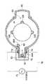
図1は本発明の係る成膜装置の一例を示す縦断面構成図、図2は成膜装置(加熱手段は省略)を示す横断面構成図である。尚、ここではシラン系ガスとしてジクロロシラン(DCS)を用い、窒化ガスとしてアンモニアガス(NH3 )を用い、上記NH3 ガスをプラズマにより活性化して窒化膜としてSiN膜を成膜する場合を例にとって説明する。Hereinafter, an embodiment of a film forming method and a film forming apparatus according to the present invention will be described in detail with reference to the accompanying drawings.
FIG. 1 is a longitudinal sectional view showing an example of a film forming apparatus according to the present invention, and FIG. 2 is a transverse sectional view showing a film forming apparatus (heating means is omitted). In this example, dichlorosilane (DCS) is used as a silane gas, ammonia gas (NH3 ) is used as a nitriding gas, and the NH3 gas is activated by plasma to form a SiN film as a nitride film. I will explain to you.
図示するように、プラズマを形成することができるこの成膜装置2は、下端が開口された有天井の円筒体状の処理容器4を有している。この処理容器4の全体は、例えば石英により形成されており、この処理容器4内の天井には、石英製の天井板6が設けられて封止されている。また、この処理容器4の下端開口部には、例えばステンレススチールにより円筒体状に成形されたマニホールド8がOリング等のシール部材10を介して連結されている。尚、ステンレス製のマニホールド8を設けないで、全体を円筒体状の石英製の処理容器で構成した装置もある。 As shown in the figure, this
上記処理容器4の下端は、上記マニホールド8によって支持されており、このマニホールド8の下方より多数枚の被処理体としての半導体ウエハWを多段に載置した保持手段としての石英製のウエハボート12が昇降可能に挿脱自在になされている。本実施例の場合において、このウエハボート12の支柱12Aには、例えば50〜100枚程度の直径が300mmのウエハWを略等ピッチで多段に支持できるようになっている。 The lower end of the processing vessel 4 is supported by the
このウエハボート12は、石英製の保温筒14を介してテーブル16上に載置されており、このテーブル16は、マニホールド8の下端開口部を開閉する例えばステンレススチール製の蓋部18を貫通する回転軸20上に支持される。
そして、この回転軸20の貫通部には、例えば磁性流体シール22が介設され、この回転軸20を気密にシールしつつ回転可能に支持している。また、蓋部18の周辺部とマニホールド8の下端部には、例えばOリング等よりなるシール部材24が介設されており、処理容器4内のシール性を保持している。The
For example, a
上記した回転軸20は、例えばボートエレベータ等の昇降機構(図示せず)に支持されたアーム26の先端に取り付けられており、ウエハボート12及び蓋部18等を一体的に昇降して処理容器4内へ挿脱できるようになされている。尚、上記テーブル16を上記蓋部18側へ固定して設け、ウエハボート12を回転させることなくウエハWの処理を行うようにしてもよい。 The rotating
このマニホールド8には、処理容器4内の方へプラズマ化される窒化ガスとして、例えばアンモニア(NH3 )ガスを供給する窒化ガス供給手段28と、成膜ガスであるシラン系ガスとして例えばDCS(ジクロロシラン)ガスを供給するシラン系ガス供給手段30と、パージガスとして不活性ガス、例えばN2 ガスを供給するパージガス供給手段36とが設けられる。具体的には、上記窒化ガス供給手段28は、上記マニホールド8の側壁を内側へ貫通して上方向へ屈曲されて延びる石英管よりなるガス分散ノズル38を有している。このガス分散ノズル38には、その長さ方向に沿って複数(多数)のガス噴射孔38Aが所定の間隔を隔てて形成されており、各ガス噴射孔38Aから水平方向に向けて略均一にアンモニアガスを噴射できるようになっている。In the
また同様に上記シラン系ガス供給手段30も、上記マニホールド8の側壁を内側へ貫通して上方向へ屈曲されて延びる石英管よりなるガス分散ノズル40を有している。このガス分散ノズル40には、その長さ方向に沿って複数(多数)のガス噴射孔40Aが所定の間隔を隔てて形成されており、各ガス噴射孔40Aから水平方向に向けて略均一にシラン系ガスであるDCSガスを噴射できるようになっている。 Similarly, the silane-based gas supply means 30 also has a
また同様に上記パージガス供給手段36は、上記マニホールド8の側壁を貫通して設けたガスノズル46を有している。上記各ノズル38、40、46には、それぞれのガス通路48、50、56が接続されている。そして、各ガス通路48、50、56には、それぞれ開閉弁48A、50A、56A及びマスフローコントローラのような流量制御器48B、50B、56Bが介設されており、NH3 ガス、DCSガス及びN2 ガスをそれぞれ流量制御しつつ供給できるようになっている。これらの各ガスの供給、供給停止、ガス流量の制御及び後述する高周波のオン・オフ制御等は例えばコンピュータ等よりなる制御手段60により行われる。またこの制御手段60は、上記制御に加え、この装置全体の動作も制御する。そして、この制御手段60は、上記制御を行うためのプログラムが記憶されているフロッピディスクやフラッシュメモリやハードディスク等よりなる記憶媒体62を有している。Similarly, the purge gas supply means 36 has a
一方、上記処理容器4の側壁の一部には、その高さ方向に沿ってプラズマを発生させて窒化ガスを活性化させる活性化手段66が形成されると共に、この活性化手段66に対向する処理容器4の反対側には、この内部雰囲気を真空排気するために処理容器4の側壁を、例えば上下方向へ削りとることによって形成した細長い排気口68が設けられている。具体的には、上記活性化手段66は、上記処理容器4の側壁を上下方向に沿って所定の幅で削りとることによって上下に細長い開口70を形成し、この開口70をその外側より覆うようにして断面凹部状になされた上下に細長い例えば石英製のプラズマ区画壁72を容器外壁に気密に溶接接合することにより形成されている。 On the other hand, an activation means 66 that activates a nitriding gas by generating plasma along the height direction is formed on a part of the side wall of the processing vessel 4 and faces the activation means 66. On the opposite side of the processing container 4, there is provided an
これにより、この処理容器4の側壁の一部を凹部状に外側へ窪ませることにより一側が処理容器4内へ開口されて連通された活性化手段66が一体的に形成されることになる。すなわちプラズマ区画壁72の内部空間は、上記処理容器4内に一体的に連通された状態となっている。上記開口70は、ウエハボート12に保持されている全てのウエハWを高さ方向においてカバーできるように上下方向に十分に長く形成されている。 As a result, a part of the side wall of the processing container 4 is recessed outward in the shape of a recess so that the activating means 66 having one side opened into the processing container 4 and communicated therewith is integrally formed. That is, the internal space of the
そして、上記プラズマ区画壁72の両側壁の外側面には、その長さ方向(上下方向)に沿って互いに対向するようにして細長い一対のプラズマ電極74が設けられると共に、このプラズマ電極74にはプラズマ発生用の高周波電源76が給電ライン78を介して接続されており、上記プラズマ電極74に例えば13.56MHzの高周波電圧を印加することによりプラズマを発生し得るようになっている。尚、この高周波電圧の周波数は13.56MHzに限定されず、他の周波数、例えば400kHz等を用いてもよい。 A pair of
そして、上記処理容器4内を上方向に延びていく窒化ガス用のガス分散ノズル38は途中で処理容器4の半径方向外方へ屈曲されて、上記プラズマ区画壁72内の一番奥(処理容器4の中心より一番離れた部分)に位置され、この一番奥の部分に沿って上方に向けて起立させて設けられている。従って、高周波電源76がオンされている時に上記ガス分散ノズル38のガス噴射孔38Aから噴射されたアンモニアガスはここで活性化されて処理容器4の中心に向けて拡散しつつ流れるようになっている。 Then, the
そして上記プラズマ区画壁72の外側には、これを覆うようにして例えば石英よりなる絶縁保護カバー80が取り付けられている。また、この絶縁保護カバー80の内側部分には、図示しない冷媒通路が設けられており、冷却された窒素ガスや冷却水を流すことにより上記プラズマ電極74を冷却し得るようになっている。
そして上記プラズマ区画壁72の開口70の外側近傍、すなわち開口70の外側(処理容器4内)には、上記シラン系ガス用のガス分散ノズル40が起立させて設けられており、このノズル40に設けた各ガス噴射孔40Aより処理容器4の中心方向に向けてシラン系ガスを噴射し得るようになっている。An insulating
A
一方、上記開口70に対向させて設けた排気口68には、これを覆うようにして石英よりなる断面コ字状に成形された排気口カバー部材82が溶接により取り付けられている。この排気口カバー部材82は、上記処理容器4の側壁に沿って上方に延びており、処理容器4の上方のガス出口84より図示しない真空ポンプや圧力調整弁等を介設した真空排気系により真空引きされる。そして、この処理容器4の外周を囲むようにしてこの処理容器4及びこの内部のウエハWを加熱する筒体状の加熱手段86が設けられている。 On the other hand, an exhaust
次に、以上のように構成された成膜装置2を用いて行なわれるプラズマによる本発明の成膜方法(いわゆるALD成膜)について説明する。
本発明方法の第1の発明では、シラン系ガスを供給するシラン系ガス供給工程と窒化ガスを供給する窒化ガス供給工程とを交互に繰り返し行うと共に、繰り返される複数の窒化ガス供給工程にはプラズマを立てる窒化ガス供給工程とプラズマを立てない窒化ガス供給工程とが含まれるようにしてシリコン窒化膜(SiN)よりなる薄膜を形成する。Next, a film forming method (so-called ALD film forming) of the present invention using plasma performed using the
In the first aspect of the method of the present invention, the silane-based gas supplying step for supplying the silane-based gas and the nitriding gas supplying step for supplying the nitriding gas are alternately repeated, and plasma is included in the repeated nitriding gas supplying steps. A thin film made of a silicon nitride film (SiN) is formed so as to include a nitriding gas supply process for forming a plasma and a nitriding gas supply process for generating no plasma.
まず、本発明方法の第1の発明について説明する。図3は本発明の成膜方法の第1の発明における各種ガスの供給のタイミングとRF(高周波)の印加タイミングを示すタイミングチャートである。尚、図3中の一部には拡大図が併記して示されている。まず、常温の多数枚、例えば50〜100枚の300mmサイズの製品用のウエハWが載置された状態のウエハボート12を予め所定の温度になされた処理容器4内にその下方より上昇させてロードし、蓋部18でマニホールド8の下端開口部を閉じることにより容器内を密閉する。 First, the first invention of the method of the present invention will be described. FIG. 3 is a timing chart showing various gas supply timings and RF (high frequency) application timings in the first aspect of the film forming method of the present invention. Note that an enlarged view is shown together in a part of FIG. First, the
そして処理容器4内を真空引きして所定のプロセス圧力に維持すると共に、加熱手段86への供給電力を増大させることにより、ウエハ温度を上昇させてプロセス温度を維持する。上記DCSガスをシラン系ガス供給手段30から供給し、そして、NH3 ガスを窒化ガス供給手段28から供給する。具体的には、図3に示すように、上記シラン系ガスを供給するシラン系ガス供給工程と上記窒化ガスを供給する窒化ガス供給工程とを交互に繰り返し行うと共に、上記繰り返される複数の窒化ガス供給工程にはプラズマを立てる窒化ガス供給工程とプラズマを立てない窒化ガス供給工程とが含まれるようにする。この際、上記シラン系ガス供給工程と窒化ガス供給工程との間には、パージを行う間欠期間を設けるようにするのがよい。尚、この間欠期間を設けなくてもよい。また隣り合うシラン系ガス供給工程同士間が1サイクルとなる。Then, the inside of the processing container 4 is evacuated and maintained at a predetermined process pressure, and the power supplied to the heating means 86 is increased to raise the wafer temperature and maintain the process temperature. The DCS gas is supplied from the silane-based gas supply means 30, and NH3 gas is supplied from the nitriding gas supply means 28. Specifically, as shown in FIG. 3, the silane-based gas supply step for supplying the silane-based gas and the nitriding gas supply step for supplying the nitriding gas are alternately repeated, and the plurality of repeated nitriding gases are repeated. The supplying process includes a nitriding gas supplying process for generating plasma and a nitriding gas supplying process for generating no plasma. At this time, it is preferable to provide an intermittent period for purging between the silane-based gas supply step and the nitriding gas supply step. This intermittent period may not be provided. One cycle is between adjacent silane-based gas supply processes.
これにより、回転しているウエハボート12に支持されているウエハWの表面にSiN薄膜を形成する。この際、NH3 ガスを供給する時に、常にプラズマを立てるようにするのではなく、プラズマを立てないで成膜するサイクルと、プラズマを立てて成膜するサイクルとが混在するように設定する。図3に示す場合には、説明を容易化するために複数、具体的には3サイクルの長さを1セット工程として定義して示している。As a result, a SiN thin film is formed on the surface of the wafer W supported by the rotating
そして、ここでは最初の第1番目のセット工程(3サイクル)では高周波電源(RF電源)62をオフしてプラズマを立てておらず、第2番目セット工程(3サイクル)ではNH3 ガスの供給と同時に高周波電源62をオンしてプラズマを立てている。以後、同様に、プラズマを立てないセット工程とプラズマを立てるセット工程とを交互に繰り返し行っている。尚、ここでは上記1セット工程を形成するサイクル数は、単に一例として3サイクルとしたが、このサイクル数に限定されず、例えば1〜10数サイクルを1セット工程として定義することができる。Here, in the first first setting step (3 cycles), the high frequency power source (RF power source) 62 is turned off and no plasma is generated, and in the second setting step (3 cycles), NH3 gas is supplied. At the same time, the high
具体的には、NH3 ガスはガス分散ノズル38の各ガス噴射孔38Aから水平方向へ噴射され、また、DCSガスはガス分散ノズル40の各ガス噴射孔40Aから水平方向へ噴射され、各ガスが反応してSiN薄膜が形成される。この場合、上記各ガスは、連続的に供給されるのではなく、図3に示すようにDCSガスは間欠的に、パルス状に供給される(シラン系ガス供給工程)。上記工程によりガスがウエハ表面に吸着されることになる。NH3 ガスは上記シラン系ガス供給工程からタイミングをずらして同じくパルス状に供給される(窒化ガス供給工程)。Specifically, NH3 gas is injected in the horizontal direction from each
そして、上記窒化ガス供給工程の前後にはパージを行う間欠期間を挟み込んでおり、SiN膜を一層ずつ繰り返し積層する。また間欠期間においては真空引きが継続されて容器内に残留するガスを排除している。そして、NH3 ガスを単独で流す時には、上述したように、1セット工程毎(3サイクル毎)にRF電源がオフされてプラズマを立てない場合と、RF電源をパルス状にオンしてプラズマを立てる場合とが繰り返し行われ、プラズマが立てられない時には反応速度が遅い状態で成膜がなされ、プラズマが立てられた時にはNH3 ガスが活性化されて活性種等が作られて反応が促進された状態で成膜がなされる。Then, before and after the nitriding gas supply step, an intermittent period in which purging is performed is interposed, and the SiN film is repeatedly laminated one by one. Further, evacuation is continued during the intermittent period to eliminate the gas remaining in the container. When the NH3 gas is allowed to flow alone, as described above, when the RF power source is turned off every one set process (every three cycles) and the plasma is not generated, the RF power source is turned on in a pulsed manner and the plasma is turned on. When the plasma is not generated, the film is formed with a slow reaction rate. When the plasma is generated, the NH3 gas is activated to generate active species and the reaction is promoted. Film formation is performed in the state.
この場合、プラズマを立てる時にはNH3 ガスの供給期間の全期間に亘ってRF電源をオンしてもよいし、図4に示すようにNH3 ガスの供給開始から所定の時間Δtが経過した後に、RF電源をオンするようにしてもよい。この所定の時間ΔtとはNH3 ガスの流量が安定するまでの時間であり、例えば5秒程度である。このように、NH3 ガスの流量が安定化した後にRF電源をオンすることにより、ウエハWの面間方向(高さ方向)における活性種の濃度均一性を向上できる。また間欠期間では、不活性ガスであるN2 ガスを処理容器4内へ供給して残留ガスを排除するようにしてもよいし(不活性ガスパージ)、或いは、全てのガスの供給を停止したまま真空引きを継続して行うことにより(バキュームとも称す)、処理容器4内の残留ガスを排除するようにしてもよい。更には、間欠期間の前半はバキュームを行い、後半は不活性ガスパージを行うようにしてもよい。In this case, when the plasma is generated, the RF power supply may be turned on over the entire NH3 gas supply period, or after a predetermined time Δt has elapsed from the start of NH3 gas supply as shown in FIG. The RF power supply may be turned on. The predetermined time Δt is a time until the flow rate of the NH3 gas is stabilized, and is about 5 seconds, for example. Thus, by turning on the RF power supply after the flow rate of the NH3 gas is stabilized, the concentration uniformity of the active species in the inter-plane direction (height direction) of the wafer W can be improved. Further, during the intermittent period, N2 gas, which is an inert gas, may be supplied into the processing container 4 to remove residual gas (inert gas purge), or the supply of all gases may be stopped. Residual gas in the processing container 4 may be removed by continuously performing vacuuming (also referred to as vacuum). Furthermore, vacuum may be performed in the first half of the intermittent period, and inert gas purge may be performed in the second half.
この場合、シラン系ガスの供給期間(シラン系ガス供給工程)T1は2〜10秒程度、窒化ガス供給期間(窒化ガス供給工程)T2は10〜20秒程度、前半の間欠期間T3は5〜15秒程度、後半の間欠期間T4は5〜15秒程度であるが、これらの各時間は単に一例を示したに過ぎず、この数値に限定されない。通常、1サイクルによって形成される膜厚は、プラズマを立てる場合と立てない場合とを平均すると、1.1〜1.3Å/サイクル程度であるので、目標膜厚が例えば500Åであるならば、450サイクル(=150セット工程)程度繰り返し行うことになる。この結果、図5に記載されたシリコン窒化膜の積層状態を示す断面図のように、ウエハWの表面にはプラズマを用いないSiN膜90A(プラズマなし)と、プラズマを用いたSiN膜90B(プラズマあり)とが交互にラミネート状に複数層に亘って成膜されることになる。 In this case, the silane-based gas supply period (silane-based gas supply process) T1 is about 2 to 10 seconds, the nitriding gas supply period (nitriding gas supply process) T2 is about 10 to 20 seconds, and the first intermittent period T3 is 5 to 5 seconds. The intermittent period T4 in the latter half of about 15 seconds is about 5 to 15 seconds, but each of these times is merely an example and is not limited to this value. Normally, the film thickness formed by one cycle is about 1.1 to 1.3 mm / cycle on average when the plasma is raised and when it is not raised, so if the target film thickness is 500 mm, for example, This is repeated for about 450 cycles (= 150 setting steps). As a result, as shown in the cross-sectional view of the stacked state of the silicon nitride films shown in FIG. 5, the SiN film 90A (no plasma) that does not use plasma and the SiN film 90B (no plasma) that uses plasma are formed on the surface of the wafer W. (With plasma) are alternately formed in a laminated manner over a plurality of layers.
このような積層されたシリコン窒化膜の形成方法によれば、パーティクルの発生を極力抑制することができると共に、形成されたシリコン窒化膜全体では、全てのNH3 ガス供給時にプラズマを用いて成膜した時のシリコン窒化膜と同等の膜質、すなわち誘電率が非常に低くて、ドライエッチング時のエッチング耐性の大きな薄膜を得ることができる。従って、この積層されたシリコン窒化膜の表面のクリーニング処理時やエッチング処理時に用いられる希フッ酸に対するエッチングレートを小さくでき、この結果、クリーニング処理時にこの薄膜が過度に削り取られることを防止して、この膜厚の制御性を向上させることが可能となる。またエッチングストッパ膜や層間絶縁膜としての機能も十分に果すことができる。According to such a method of forming a laminated silicon nitride film, the generation of particles can be suppressed as much as possible, and the entire formed silicon nitride film is formed using plasma when supplying all NH3 gas. As a result, it is possible to obtain a thin film having the same film quality as that of the silicon nitride film, that is, having a very low dielectric constant and high etching resistance during dry etching. Therefore, the etching rate for dilute hydrofluoric acid used during the cleaning process or etching process of the surface of the laminated silicon nitride film can be reduced, and as a result, the thin film can be prevented from being excessively scraped off during the cleaning process, This controllability of the film thickness can be improved. Also, it can sufficiently function as an etching stopper film and an interlayer insulating film.
ここで上記成膜処理のプロセス条件について説明すると、DCSガスの流量は50〜2000sccmの範囲内、例えば1000sccm(1slm)であり、NH3 ガスの流量は500〜5000sccmの範囲内、例えば1000sccmである。Here, the process conditions of the film forming process will be described. The flow rate of DCS gas is in the range of 50 to 2000 sccm, for example, 1000 sccm (1 slm), and the flow rate of NH3 gas is in the range of 500 to 5000 sccm, for example, 1000 sccm. .
またプロセス温度はCVD成膜処理よりも低い温度であり、具体的には25℃〜700℃の範囲内、好ましくは450〜630℃の範囲内である。このプロセス温度が300℃よりも低いと、反応が生ぜずにほとんど膜が堆積せず、また700℃よりも高い場合には、膜質の劣るCVDによる堆積膜が形成されてしまうのみならず、前工程ですでに形成されている金属膜等に熱的ダメージを与えてしまう。 Further, the process temperature is lower than the CVD film forming treatment, and specifically, is in the range of 25 ° C. to 700 ° C., preferably in the range of 450 to 630 ° C. When the process temperature is lower than 300 ° C., no reaction occurs and almost no film is deposited. When the process temperature is higher than 700 ° C., not only a CVD deposited film with poor film quality is formed, but also The metal film already formed in the process will be thermally damaged.
またプロセス圧力は13Pa(0.1Torr)〜13300Pa(100Torr)の範囲内、好ましくは40Pa(0.3Torr)〜266Pa(2Torr)の範囲内、より好ましくは93P(0.7Torr)〜107P(0.8Torr)の範囲内であり、例えばシラン系ガス供給工程では1Torr、窒化ガス供給工程では0.3Torrである。ここでプロセス圧力が13Paよりも小さい場合には、成膜レートが実用レベル以下になってしまう。またプロセス圧力が13300Paまでは、ウエハWに対する反応は吸着反応が主流であるので、膜質が良好な薄膜を高い成膜速度で安定的に堆積させることができ、良好な結果を得ることができる。 The process pressure is in the range of 13 Pa (0.1 Torr) to 13300 Pa (100 Torr), preferably in the range of 40 Pa (0.3 Torr) to 266 Pa (2 Torr), more preferably 93 P (0.7 Torr) to 107 P (0. 8 Torr), for example, 1 Torr in the silane-based gas supply process and 0.3 Torr in the nitriding gas supply process. Here, when the process pressure is smaller than 13 Pa, the film forming rate becomes below the practical level. Further, since the reaction with respect to the wafer W is mainly an adsorption reaction up to a process pressure of 13300 Pa, a thin film having a good film quality can be stably deposited at a high film formation rate, and a good result can be obtained.
しかし、プロセス圧力が13300Paよりも大きくなると、反応形態が吸着反応から気相反応へ移行してこの気相反応が主流となり、この結果、膜厚の面間及び面内均一性が低下するのみならず、気相反応に起因するパーティクルが急激に増大するので好ましくない。 However, if the process pressure becomes higher than 13300 Pa, the reaction form shifts from an adsorption reaction to a gas phase reaction, and this gas phase reaction becomes the mainstream. As a result, only the inter-surface and in-plane uniformity of the film thickness decreases. In addition, the particles resulting from the gas phase reaction increase rapidly, which is not preferable.
このように、本発明方法の第1の発明によれば、シラン系ガスを供給するシラン系ガス供給工程と窒化ガスを供給する窒化ガス供給工程とを交互に繰り返し行うと共に、繰り返される複数の窒化ガス供給工程にはプラズマを立てる窒化ガス供給工程とプラズマを立てない窒化ガス供給工程とが含まれているようにしたので、パーティクルの発生を抑制しつつ絶縁性が高くてエッチングレートが低い等のように膜質が良好で、しかも成膜レートも高いシリコン窒化膜を形成することができる。 As described above, according to the first aspect of the method of the present invention, the silane-based gas supplying step for supplying the silane-based gas and the nitriding gas supplying step for supplying the nitriding gas are alternately and repeatedly performed. Since the gas supply process includes a nitriding gas supply process that generates plasma and a nitriding gas supply process that does not generate plasma, the generation of particles is suppressed and the insulating property is high and the etching rate is low. Thus, a silicon nitride film having a good film quality and a high film formation rate can be formed.
尚、上記実施例では、1セット工程(=3サイクル)毎に、プラズマを用いない窒化ガス供給工程とプラズマを用いた窒化ガス供給工程とを交互に繰り返すようにしたが、これに限定されず、3セット工程で1回の割合、4セット工程で1回の割合、或いはそれ以上の数のセット工程で1回の割合でプラズマを用いない窒化ガス供給工程を行うようにしてもよい。
ただし、プラズマを用いない窒化ガス供給工程が過度に多くなると、膜質特性が劣化し、逆に過度に少なくなり過ぎると、パーティクルの発生が急激に増加してしまう。In the above-described embodiment, the nitriding gas supply process that does not use plasma and the nitriding gas supply process that uses plasma are alternately repeated every one set process (= 3 cycles). However, the present invention is not limited to this. The nitriding gas supply step that does not use plasma may be performed at a rate of once in 3 set steps, once at a rate of 4 set steps, or once at a rate of more than one set step.
However, if the number of nitriding gas supply steps without using plasma is excessively increased, the film quality characteristics deteriorate, and conversely, if the amount is excessively decreased, the generation of particles is rapidly increased.
<本発明方法の第1の発明によるシリコン窒化膜の評価>
ここで上述した本発明方法の第1の方法発明により形成したシリコン窒化膜の評価を行ったので、その評価結果について説明する。ここでは比較のために、窒化ガスであるNH3 ガスの全ての供給時にプラズマを立てて形成した時のシリコン窒化膜及びNH3 ガスの全ての供給時にプラズマを立てないで形成した時のシリコン窒化膜をそれぞれ基準として併記している。<Evaluation of the silicon nitride film according to the first aspect of the method of the present invention>
Here, since the silicon nitride film formed by the first method invention of the present invention described above was evaluated, the evaluation result will be described. For comparison, here, for the purpose of comparison, the silicon nitride film formed when plasma is formed when all the NH3 gas that is a nitriding gas is supplied and the silicon nitride film formed when plasma is not generated when all the NH3 gas is supplied. The membranes are also shown as references.
図6はシリコン窒化膜の成膜処理における窒化ガス供給工程のプラズマの有無を示す図である。ここで図6中の1区画が1セット行程を表し、斜線部分は窒化ガス供給工程の時にプラズマを用いた場合を示し、空白部分は窒化ガス供給工程の時にプラズマを用いない場合を示している。そして、図6中の右方向が時間の経過方向となる。従って、図6(A)に示す基準1は全ての窒化ガス供給工程にてプラズマを用いた場合を示し、図6(B)に示す基準2は全ての窒化ガス供給工程にてプラズマを用いない場合を示し、図6(C)に示す実施例1は2セット工程で1回の割合で窒化ガス供給工程にてプラズマを用いない場合を示し、図6(D)に示す実施例2は3セット工程で1回の割合で窒化ガス供給工程にてプラズマを用いない場合を示し、図6(E)に示す実施例3は4セット工程で1回の割合で窒化ガス供給工程にてプラズマを用いない場合を示している。 FIG. 6 is a diagram showing the presence or absence of plasma in the nitriding gas supply step in the silicon nitride film forming process. Here, one section in FIG. 6 represents one set process, the hatched portion indicates the case where plasma is used during the nitriding gas supply step, and the blank portion indicates the case where plasma is not used during the nitriding gas supply step. . And the right direction in FIG. 6 becomes the passage direction of time. Therefore, the
尚、図3に示すフローチャートは、1セット工程中のサイクル数は異なるが、図6(C)に示す実施例1の場合を示している。また、ここでの1セット工程のサイクル数は1サイクルに設定している。そして、ここでは目標膜厚は500Å程度に設定している。 The flowchart shown in FIG. 3 shows the case of Example 1 shown in FIG. 6C, although the number of cycles in one set process is different. In addition, the number of cycles in one set process here is set to one cycle. Here, the target film thickness is set to about 500 mm.
ここで計測したパーティクルのサイズは0.08〜1.00μmであり、また図7中のTOPはウエハボートの上段に位置するウエハを示し、CTRは中段に位置するウエハを示し、BTMは下段に位置するウエハを示す。この点は、図7以降の図示例においても同じである。
さて、図6に示すようなプラズマ使用態様のもとでシリコン窒化膜を形成した時のパーティクル発生状況を図7に示す。ここでは同一の成膜装置内で基準1→基準2→実施例1→実施例2→実施例3の順序で成膜処理を行っている。The size of the particles measured here is 0.08 to 1.00 μm, and TOP in FIG. 7 indicates the wafer located at the upper stage of the wafer boat, CTR indicates the wafer located at the middle stage, and BTM indicates the lower stage. The wafer being positioned is shown. This also applies to the illustrated examples in FIG.
Now, FIG. 7 shows the state of particle generation when the silicon nitride film is formed under the plasma usage mode shown in FIG. Here, the film forming process is performed in the order of
この図7に示すように、全ての窒化ガス供給工程でプラズマを用いた基準1の場合には、ウエハボートの全範囲においてパーティクル数が300個以上になっており、パーティクルが多量に発生して好ましくないことが判る。尚、この場合、シリコン窒化膜の膜質特性はかなり良好であった。
また全ての窒化ガス供給工程でプラズマを用いなかった基準2の場合には、ウエハボートの全域に亘ってパーティクル数が十数個程度であって非常に少なく良好であるが、この場合、形成されたシリコン窒化膜の膜質特性は良好ではなかった。As shown in FIG. 7, in the case of the
Further, in the case of the standard 2 in which plasma is not used in all the nitriding gas supply processes, the number of particles is about a dozen or so over the entire area of the wafer boat, which is very small. The film quality characteristics of the silicon nitride film were not good.
次に、本発明の実施例1〜3の場合では、実施例1〜3になるに従って、すなわち窒化ガス供給工程でプラズマを用いる比率が順次多くなるに従って、パーティクル数は少しずつ増加するが、それでも基準1の場合よりは遥かに少なくて良好な結果が示されている。この場合、形成されたシリコン窒化膜の膜質特性もそれぞれ比較的良好であった。 Next, in the case of Examples 1 to 3 of the present invention, the number of particles increases little by little as the Examples 1 to 3 are increased, that is, as the ratio of using plasma in the nitriding gas supply step is sequentially increased. Better results are shown, far less than for
次に、シリコン窒化膜のストレスの評価結果について説明する。図8は図6に示すプラズマ使用態様のもとで形成されたシリコン窒化膜のストレスを示すグラフである。この膜ストレスが大きい場合は、形成されたシリコン窒化膜に割れが入って剥がれ易く、パーティクルの発生原因の1つになっている。 Next, the stress evaluation result of the silicon nitride film will be described. FIG. 8 is a graph showing the stress of the silicon nitride film formed under the plasma usage mode shown in FIG. When this film stress is large, the formed silicon nitride film is easily cracked and peeled off, which is one of the causes of generation of particles.
図8に示すように、全ての窒化ガス供給工程でプラズマを用いた基準1は、他の基準2及び実施例1〜3よりもストレスが遥かに高くて0.621GPa程度に達している。このように基準1の膜ストレスが大きいことが、図7において説明したように、基準1のパーティクル数の発生個数が多いことの理由の1つとなっている、ということを理解することができる。 As shown in FIG. 8, the standard 1 using plasma in all the nitriding gas supply steps is much higher than the
そして、基準2及び実施例1〜3の膜ストレスはプラズマを何ら用いていない基準2の場合が最小であり、窒化ガス供給工程においてプラズマを使用する比率が大きくなるに従って、膜ストレスも少しずつ増加しているが、それでも実施例3における0.404GPaが最大であり、この値は上記基準1の場合よりも遥かに小さくなっていることを、確認することができた。このように膜ストレスが小さいことが、図7中において基準2、実施例1〜3のパーティクル数を抑制できることの理由の1つとなっていることが判る。また、窒化ガス供給工程におけるプラズマを立てる比率を変えることにより、膜ストレスをコントロールすることができる。 The film stress of the
次に、シリコン窒化膜の成膜レートと膜厚均一性についての評価結果を説明する。図9は図6に示すプラズマ使用態様のもとで形成されたシリコン窒化膜の成膜レートと膜厚の面間均一性及び面内均一性を示すグラフである。図9中において棒グラフは成膜レートを示し、”□”よりなる折れ線グラフは膜厚の面内均一性を示し、”◇”よりなるポイントは膜厚の面間均一性を示す。 Next, evaluation results for the film formation rate and film thickness uniformity of the silicon nitride film will be described. FIG. 9 is a graph showing the inter-plane uniformity and in-plane uniformity of the deposition rate and film thickness of the silicon nitride film formed under the plasma usage mode shown in FIG. In FIG. 9, the bar graph shows the film formation rate, the line graph made of “□” shows the in-plane uniformity of the film thickness, and the point made of “◇” shows the inter-surface uniformity of the film thickness.
図9に示すように、基準1の場合はプラズマを多く用いていることからNH3 ガスの活性化が促進されて成膜レートが大きくて1.26Å/サイクル程度になっている。そして、基準2の場合はプラズマを全く用いないことから成膜レートは小さくて0.89Å/サイクル程度になっている。これに対して、本発明の実施例1〜3の場合は、基準1よりは小さいが基準2よりは遥かに大きくて実施例1が1.11Å/サイクルであり、窒化ガス供給工程でプラズマを立てる比率が増加するに従って、成膜レートも次第に大きくなり、結果的に実施例3では1.19Å/サイクル程度まで大きくなっており、良好な結果を示していることが判る。As shown in FIG. 9, in the case of
また膜厚の面内均一性は、TOP、CTR、BTMの各位置で変化はあるが、基準1〜実施例3まで同じ傾向を示して比較的小さくなっている。また膜厚の面間均一性に関しては、基準1及び基準2がそれぞれ±1%以下であるのに対して、本発明の実施例1〜3ではそれぞれ±1%よりも小さく、良好な結果を示していることが判る。 Further, the in-plane uniformity of the film thickness changes at each position of TOP, CTR, and BTM, but is relatively small with the same tendency from the
次に、膜質特性の1つであるエッチングレートの評価結果を説明する。図10は図6に示すプラズマ使用態様のもとで形成されたシリコン窒化膜のエッチングレートを示すグラフである。ここではエッチング液として0.5%の希フッ酸(0.5%DHF)を用いた。尚、基準1の場合には”CTR”における結果のみを示す。 Next, the evaluation result of the etching rate which is one of the film quality characteristics will be described. FIG. 10 is a graph showing the etching rate of the silicon nitride film formed under the plasma usage mode shown in FIG. Here, 0.5% dilute hydrofluoric acid (0.5% DHF) was used as an etchant. In the case of
図10から明らかなように、窒化ガス供給工程でプラズマを全く用いない基準2のエッチングレートは5.92Å/min程度で比較的大きい。これに対して、本発明の実施例1〜3ではエッチングレートは5.25〜5.45Å/min程度であって上記基準2よりも小さく、そして膜質が良好な基準1の5.53Å/minと同じ程度の値であり、実施例1〜3のエッチングレートは上述のようにかなり小さくて良好な特性を示していることが判る。 As is clear from FIG. 10, the etching rate of the
上記実施例では、図3に示すように1サイクルの中で先にDCSを供給したが、これに替えて先にNH3 ガスを供給するようにしてもよい。また、同様に、第2番目のセット工程で初めてプラズマを立てたが、これに替えて、第1番目のセット工程でプラズマを立てるようにしてもよい。In the above embodiment, DCS is supplied first in one cycle as shown in FIG. 3, but NH3 gas may be supplied first instead. Similarly, the plasma is generated for the first time in the second setting step. Instead, plasma may be generated in the first setting step.
また、ここでは図6に示すプラズマを用いた評価実験との関係で1セット工程を単位としてプラズマをオン又はオフする場合を例にとって説明したが、これに限らず、例えば図11に示すように、1サイクルを単位としてプラズマをオン又はオフするようにしてもよい。図11は1サイクルを単位として各種ガスの供給タイミングとRFの印加タイミングを示すタイミングチャートである。例えば図11(A)に示す場合のように、パルス状に行われる窒化ガス供給工程において1つ置きに、すなわち交互にRF(高周波電圧)を印加してプラズマを立てるようにしてもよい。 Further, here, the case where the plasma is turned on or off in units of one set process in relation to the evaluation experiment using the plasma shown in FIG. 6 has been described as an example. However, the present invention is not limited to this. For example, as shown in FIG. The plasma may be turned on or off in units of one cycle. FIG. 11 is a timing chart showing various gas supply timings and RF application timings in units of one cycle. For example, as shown in FIG. 11A, plasma may be generated by applying RF (radio frequency voltage) every other time, that is, alternately in a nitriding gas supply step performed in a pulsed manner.
また図11(B)に示す場合のように、パルス状に行われる窒化ガス供給工程の3回の内の2回の比率でRFを印加してプラズマを立てるようにしてもよい。いずれにしても、パーティクルが発生しないようにプラズマを立てる窒化ガス供給工程とプラズマを立てない窒化ガス供給工程とが混在するようにすればよく、パルス状に配列される窒化ガス供給工程の内のどの位置でプラズマを立てないようにするかは、特に限定されるものではない。このように、いずれにしても一連の成膜処理の間にプラズマを用いない窒化ガス供給工程を適度に組み込むことにより、パーティクルの発生を抑制しつつ膜質特性の良好なシリコン窒化膜を得ることができる。 Further, as shown in FIG. 11B, plasma may be generated by applying RF at a ratio of two out of three nitriding gas supply steps performed in a pulsed manner. In any case, a nitriding gas supply process for generating plasma so as not to generate particles and a nitriding gas supply process for not generating plasma may be mixed. The position where plasma is not generated is not particularly limited. In this way, in any case, a silicon nitride film having good film quality characteristics can be obtained while suppressing generation of particles by appropriately incorporating a nitriding gas supply process that does not use plasma during a series of film forming processes. it can.
<成膜方法の第2の発明>
上記第1の発明では、処理容器4内に、実際に製品となる半導体ウエハWが収容されている状態で、シリコン系ガスや窒化ガスを流して成膜する場合について説明したが、これに限定されず、上記成膜処理を行う前にこの処理容器4内へ製品となる半導体ウエハWを収容しない状態で上記各ガスを供給してプリコート形成処理を行うようにしてもよい。<Second Invention of Film Formation Method>
In the first aspect of the invention, the case where the film is formed by flowing a silicon-based gas or a nitriding gas in the state where the semiconductor wafer W that is actually a product is accommodated in the processing container 4 has been described. However, the present invention is not limited thereto. Instead, before performing the film formation process, the precoat formation process may be performed by supplying each gas in a state where the semiconductor wafer W as a product is not accommodated in the process container 4.
すなわち、先の第1の発明で説明した成膜処理の前段、例えば成膜処理の直前の工程で上記プリコート形成処理を行う。このプリコート形成処理は、上述したように、上記処理容器4内に上記被処理体Wを収容しない状態で上記シラン系ガスを供給するシラン系ガス供給工程と、プラズマを立てないで上記窒化ガスを供給する窒化ガス供給工程とを交互に繰り返し行う。 That is, the precoat forming process is performed in a stage preceding the film forming process described in the first aspect of the invention, for example, a process immediately before the film forming process. As described above, the precoat forming process includes a silane-based gas supply step of supplying the silane-based gas in a state where the object to be processed W is not accommodated in the processing container 4, and the nitriding gas without generating plasma. The supplying nitriding gas supplying step is alternately repeated.
具体的には、処理容器4内のウエハボート12上には何ら載置しないで空の状態で、或いは製品用の半導体ウエハではなく製品として用いない半導体ウエハ、すなわちダミーウエハを載置した状態で、上記プリコート形成処理を行う。このプリコート形成処理では、図3に示すようにシラン系ガス供給工程と窒化ガス供給工程とを交互に繰り返して行うが、この場合、窒化ガス供給工程では何らプラズマを立てないようにする。すなわち、このプリコート形成処理では高周波電源は全く使用しない状態となる。他のプロセス圧力やプロセス温度等のプロセス条件は、製品ウエハに対する成膜時のプロセス条件と同じである。 Specifically, in a state where nothing is placed on the
これにより、処理容器4の内壁面やウエハボート12等の容器内構造物の表面にプラズマを用いないで形成されたシリコン窒化膜よりなるプリコート膜が施されることになる。このプリコート形成処理後の製品ウエハに対する成膜処理は、先の第1の発明において説明した内容で行われることになる。また、このようにプリコート形成処理を行った場合には、予め処理容器4内の表面にプリコート膜が形成されているので、製品ウエハに対する成膜処理における全ての窒化ガス供給工程にてプラズマを立てるようにしてもよい。 As a result, a precoat film made of a silicon nitride film formed without using plasma is applied to the inner wall surface of the processing container 4 and the surface of the internal structure of the container such as the
このように、シリコン窒化膜を形成するに際して、プラズマを用いないでプリコートを形成するプリコート形成処理を行い、その後に、処理容器4内へ被処理体であるウエハWを収容した状態でシラン系ガスを供給するシラン系ガス供給工程と、窒化ガスを供給する窒化ガス供給工程とを交互に繰り返し行うと共に、繰り返される複数の窒化ガス供給工程にはプラズマを立てる窒化ガス供給工程とプラズマを立てない窒化ガス供給工程とが含まれているようにしたので、パーティクルの発生を抑制しつつ絶縁性が高くてエッチングレートが低い等のように膜質が良好で、しかも成膜レートも高いシリコン窒化膜を形成することができる。 As described above, when forming the silicon nitride film, a precoat forming process for forming a precoat without using plasma is performed, and then the wafer W as the object to be processed is accommodated in the processing container 4. A silane-based gas supply step for supplying nitrogen and a nitriding gas supply step for supplying nitriding gas are alternately repeated, and a nitriding gas supplying step for generating plasma and a nitriding without plasma for a plurality of repeated nitriding gas supplying steps The gas supply process is included, so the formation of silicon nitride films with good film quality and high film formation rate, such as high insulation and low etching rate, while suppressing the generation of particles. can do.
尚、ここではシリコン窒化膜としてSiN膜を成膜する場合を例にとって説明したが、これに限定されず、不純物ドープ用のガス、例えばボロン含有ガスや炭化水素ガス等を供給して、B及び/又はC等の不純物がドープされたシリコン窒化膜を形成するような場合にも、本発明を適用することができる。 Here, the case where a SiN film is formed as a silicon nitride film has been described as an example. However, the present invention is not limited to this, and an impurity doping gas such as a boron-containing gas or a hydrocarbon gas is supplied, and B and The present invention can also be applied to the case where a silicon nitride film doped with impurities such as C is formed.
また上記各実施例では、シラン系ガスとしてDCSガスを用いたが、これに限定されず、ジクロロシラン(DCS)、ヘキサクロロジシラン(HCD)、モノシラン[SiH4 ]、ジシラン[Si2 H6 ]、ヘキサメチルジシラザン(HMDS)、テトラクロロシラン(TCS)、ジシリルアミン(DSA)、トリシリルアミン(TSA)、ビスターシャルブチルアミノシラン(BTBAS)、トリメチルシラン(TMS)、ジメチルシラン(DMS)、モノメチルアミン(MMA)よりなる群より選択される1以上のガスを用いることができる。In each of the above embodiments, DCS gas is used as the silane-based gas. However, the present invention is not limited to this, and dichlorosilane (DCS), hexachlorodisilane (HCD), monosilane [SiH4 ], disilane [Si2 H6 ], Hexamethyldisilazane (HMDS), tetrachlorosilane (TCS), disilylamine (DSA), trisilylamine (TSA), binary butylaminosilane (BTBAS), trimethylsilane (TMS), dimethylsilane (DMS), monomethylamine (MMA) One or more gases selected from the group consisting of:
また、上記各実施例では、窒化ガスとしてNH3 ガスを用いたが、これに限定されず、アンモニア[NH3 ]、窒素[N2 ]、一酸化二窒素[N2 O]、一酸化窒素[NO]よりなる群より選択される1以上のガスを用いることができる。
また被処理体としては、半導体ウエハに限定されず、ガラス基板やLCD基板等にも本発明を適用することができる。In each of the above embodiments, NH3 gas is used as the nitriding gas. However, the present invention is not limited to this. Ammonia [NH3 ], nitrogen [N2 ], dinitrogen monoxide [N2 O], and nitric oxide One or more gases selected from the group consisting of [NO] can be used.
The object to be processed is not limited to a semiconductor wafer, and the present invention can be applied to a glass substrate, an LCD substrate, and the like.
2 成膜装置
4 処理容器
12 ウエハボート(保持手段)
18 蓋部
28 窒化ガス供給手段
30 シラン系ガス供給手段
36 パージガス供給手段
38,40 ガス分散ノズル
60 制御手段
62 記憶媒体
66 活性化手段
74 プラズマ電極
76 高周波電源
86 加熱手段
W 半導体ウエハ(被処理体)
2 Film deposition apparatus 4
Claims (19)
Translated fromJapanese前記シラン系ガスを供給するシラン系ガス供給工程と前記窒化ガスを供給する窒化ガス供給工程とを交互に繰り返し行うと共に、前記繰り返される複数の窒化ガス供給工程にはプラズマを立てる窒化ガス供給工程とプラズマを立てない窒化ガス供給工程とが含まれていることを特徴とする成膜方法。Forming a thin film made of a silicon nitride film on the surface of the object to be processed by supplying a silane-based gas and a nitriding gas into a processing container in which a plurality of objects to be processed are accommodated and capable of being evacuated In a film forming method in which processing is performed,
A nitriding gas supply step of alternately supplying a silane-based gas supply step of supplying the silane-based gas and a nitriding gas supply step of supplying the nitriding gas, and generating plasma in the plurality of repeated nitriding gas supply steps; And a nitriding gas supply step that does not generate plasma.
前記処理容器内に前記被処理体を収容しない状態で前記シラン系ガスを供給するシラン系ガス供給工程と、プラズマを立てないで前記窒化ガスを供給する窒化ガス供給工程とを交互に繰り返し行うプリコート形成処理を行い、
その後に、前記処理容器内へ前記被処理体を収容した状態で前記シラン系ガスを供給するシラン系ガス供給工程と、前記窒化ガスを供給する窒化ガス供給工程とを交互に繰り返し行うと共に、前記繰り返される複数の窒化ガス供給工程にはプラズマを立てる窒化ガス供給工程とプラズマを立てない窒化ガス供給工程とが含まれていることを特徴とする成膜方法。Forming a thin film made of a silicon nitride film on the surface of the object to be processed by supplying a silane-based gas and a nitriding gas into a processing container in which a plurality of objects to be processed are accommodated and capable of being evacuated In a film forming method in which processing is performed,
Pre-coating in which a silane-based gas supply step for supplying the silane-based gas without containing the object to be processed in the processing container and a nitriding gas supply step for supplying the nitriding gas without generating plasma are alternately performed. Perform the formation process,
Thereafter, alternately performing a silane-based gas supply step of supplying the silane-based gas and a nitriding gas supply step of supplying the nitriding gas in a state where the object to be processed is accommodated in the processing container, A film forming method characterized in that the plurality of repeated nitriding gas supplying steps include a nitriding gas supplying step for generating plasma and a nitriding gas supplying step for not generating plasma.
真空引き可能になされた縦型の筒体状の処理容器と、
前記被処理体を複数段に保持して前記処理容器内に挿脱される保持手段と、
前記処理容器の外周に設けられる加熱手段と、
前記処理容器内へシラン系ガスを供給するシラン系ガス供給手段と、
前記処理容器内へ窒化ガスを供給する窒化ガス供給手段と、
前記窒化ガスを活性化する活性化手段と、
請求項1乃至15のいずれかに記載した成膜方法を実行するように制御する制御手段と、
を備えたことを特徴とする成膜装置。In a film forming apparatus for forming a predetermined thin film on an object to be processed,
A vertical cylindrical processing container made evacuated,
Holding means for holding the object to be processed in a plurality of stages and being inserted into and removed from the processing container;
Heating means provided on the outer periphery of the processing container;
A silane-based gas supply means for supplying a silane-based gas into the processing vessel;
Nitriding gas supply means for supplying a nitriding gas into the processing vessel;
Activating means for activating the nitriding gas;
Control means for controlling to execute the film forming method according to claim 1;
A film forming apparatus comprising:
請求項1乃至15のいずれかに記載の成膜方法を実行するように前記成膜装置を制御するコンピュータ読み取り可能なプログラムを記憶することを特徴とする記憶媒体。A film forming apparatus for forming a SiN thin film on the surface of a target object by supplying a silane-based gas and a nitriding gas into a processing container in which a plurality of target objects are accommodated and can be evacuated. When forming a thin film using
A storage medium that stores a computer-readable program for controlling the film forming apparatus so as to execute the film forming method according to claim 1.
Priority Applications (6)
| Application Number | Priority Date | Filing Date | Title |
|---|---|---|---|
| JP2007153735AJP5151260B2 (en) | 2007-06-11 | 2007-06-11 | Film forming method and film forming apparatus |
| US12/155,678US20080311760A1 (en) | 2007-06-11 | 2008-06-06 | Film formation method and apparatus for semiconductor process |
| TW097121453ATWI478238B (en) | 2007-06-11 | 2008-06-09 | Film forming method and semiconductor process device |
| KR1020080054102AKR101086588B1 (en) | 2007-06-11 | 2008-06-10 | Film forming method and apparatus for semiconductor processing and computer readable medium |
| CN2008101428745ACN101325160B (en) | 2007-06-11 | 2008-06-11 | Film formation method and apparatus for semiconductor process |
| US12/852,094US8178448B2 (en) | 2007-06-11 | 2010-08-06 | Film formation method and apparatus for semiconductor process |
Applications Claiming Priority (1)
| Application Number | Priority Date | Filing Date | Title |
|---|---|---|---|
| JP2007153735AJP5151260B2 (en) | 2007-06-11 | 2007-06-11 | Film forming method and film forming apparatus |
Publications (2)
| Publication Number | Publication Date |
|---|---|
| JP2008306093A JP2008306093A (en) | 2008-12-18 |
| JP5151260B2true JP5151260B2 (en) | 2013-02-27 |
Family
ID=40132751
Family Applications (1)
| Application Number | Title | Priority Date | Filing Date |
|---|---|---|---|
| JP2007153735AActiveJP5151260B2 (en) | 2007-06-11 | 2007-06-11 | Film forming method and film forming apparatus |
Country Status (5)
| Country | Link |
|---|---|
| US (2) | US20080311760A1 (en) |
| JP (1) | JP5151260B2 (en) |
| KR (1) | KR101086588B1 (en) |
| CN (1) | CN101325160B (en) |
| TW (1) | TWI478238B (en) |
Families Citing this family (79)
| Publication number | Priority date | Publication date | Assignee | Title |
|---|---|---|---|---|
| JP4943047B2 (en) | 2006-04-07 | 2012-05-30 | 東京エレクトロン株式会社 | Processing apparatus and processing method |
| JP5008957B2 (en)* | 2006-11-30 | 2012-08-22 | 東京エレクトロン株式会社 | Silicon nitride film forming method, forming apparatus, forming apparatus processing method, and program |
| JP2010183069A (en)* | 2009-01-07 | 2010-08-19 | Hitachi Kokusai Electric Inc | Manufacturing method of semiconductor device and substrate processing apparatus |
| JP5158068B2 (en)* | 2009-02-20 | 2013-03-06 | 東京エレクトロン株式会社 | Vertical heat treatment apparatus and heat treatment method |
| JP5346904B2 (en) | 2009-11-27 | 2013-11-20 | 東京エレクトロン株式会社 | Vertical film forming apparatus and method of using the same |
| JP5250600B2 (en)* | 2009-11-27 | 2013-07-31 | 東京エレクトロン株式会社 | Film forming method and film forming apparatus |
| US9390909B2 (en) | 2013-11-07 | 2016-07-12 | Novellus Systems, Inc. | Soft landing nanolaminates for advanced patterning |
| US9076646B2 (en) | 2010-04-15 | 2015-07-07 | Lam Research Corporation | Plasma enhanced atomic layer deposition with pulsed plasma exposure |
| US9892917B2 (en) | 2010-04-15 | 2018-02-13 | Lam Research Corporation | Plasma assisted atomic layer deposition of multi-layer films for patterning applications |
| US8637411B2 (en) | 2010-04-15 | 2014-01-28 | Novellus Systems, Inc. | Plasma activated conformal dielectric film deposition |
| US20110256734A1 (en) | 2010-04-15 | 2011-10-20 | Hausmann Dennis M | Silicon nitride films and methods |
| US8956983B2 (en) | 2010-04-15 | 2015-02-17 | Novellus Systems, Inc. | Conformal doping via plasma activated atomic layer deposition and conformal film deposition |
| US9373500B2 (en) | 2014-02-21 | 2016-06-21 | Lam Research Corporation | Plasma assisted atomic layer deposition titanium oxide for conformal encapsulation and gapfill applications |
| US9997357B2 (en) | 2010-04-15 | 2018-06-12 | Lam Research Corporation | Capped ALD films for doping fin-shaped channel regions of 3-D IC transistors |
| US9611544B2 (en) | 2010-04-15 | 2017-04-04 | Novellus Systems, Inc. | Plasma activated conformal dielectric film deposition |
| US9257274B2 (en) | 2010-04-15 | 2016-02-09 | Lam Research Corporation | Gapfill of variable aspect ratio features with a composite PEALD and PECVD method |
| US9685320B2 (en) | 2010-09-23 | 2017-06-20 | Lam Research Corporation | Methods for depositing silicon oxide |
| US8076250B1 (en)* | 2010-10-06 | 2011-12-13 | Applied Materials, Inc. | PECVD oxide-nitride and oxide-silicon stacks for 3D memory application |
| TWI562204B (en)* | 2010-10-26 | 2016-12-11 | Hitachi Int Electric Inc | Substrate processing apparatus, semiconductor device manufacturing method and computer-readable recording medium |
| US8647993B2 (en) | 2011-04-11 | 2014-02-11 | Novellus Systems, Inc. | Methods for UV-assisted conformal film deposition |
| US9165761B2 (en)* | 2011-08-25 | 2015-10-20 | Hitachi Kokusai Electric Inc. | Method for manufacturing semiconductor device, method for processing substrate, substrate processing apparatus and recording medium |
| KR101380240B1 (en) | 2011-11-17 | 2014-04-03 | 주식회사 유진테크 | Apparatus for processing substrate including heat-shield plate |
| CN102394222B (en)* | 2011-11-24 | 2016-05-04 | 上海华虹宏力半导体制造有限公司 | Prevent the method for solid particle formation on wafer surface |
| KR101371435B1 (en)* | 2012-01-04 | 2014-03-12 | 주식회사 유진테크 | Apparatus for processing substrate including processing unit |
| US8592328B2 (en) | 2012-01-20 | 2013-11-26 | Novellus Systems, Inc. | Method for depositing a chlorine-free conformal sin film |
| JP5842750B2 (en)* | 2012-06-29 | 2016-01-13 | 東京エレクトロン株式会社 | Film forming method, film forming apparatus, and storage medium |
| US9064694B2 (en) | 2012-07-12 | 2015-06-23 | Tokyo Electron Limited | Nitridation of atomic layer deposited high-k dielectrics using trisilylamine |
| KR102207992B1 (en) | 2012-10-23 | 2021-01-26 | 램 리써치 코포레이션 | Sub-saturated atomic layer deposition and conformal film deposition |
| SG2013083241A (en) | 2012-11-08 | 2014-06-27 | Novellus Systems Inc | Conformal film deposition for gapfill |
| JP6538300B2 (en) | 2012-11-08 | 2019-07-03 | ノベラス・システムズ・インコーポレーテッドNovellus Systems Incorporated | Method for depositing a film on a sensitive substrate |
| US9564309B2 (en) | 2013-03-14 | 2017-02-07 | Asm Ip Holding B.V. | Si precursors for deposition of SiN at low temperatures |
| US9824881B2 (en)* | 2013-03-14 | 2017-11-21 | Asm Ip Holding B.V. | Si precursors for deposition of SiN at low temperatures |
| US20140273530A1 (en)* | 2013-03-15 | 2014-09-18 | Victor Nguyen | Post-Deposition Treatment Methods For Silicon Nitride |
| US10297481B2 (en)* | 2013-03-21 | 2019-05-21 | Tokyo Electron Limited | Magnetic annealing apparatus |
| JP6011420B2 (en)* | 2013-03-29 | 2016-10-19 | 東京エレクトロン株式会社 | Operation method of vertical heat treatment apparatus, vertical heat treatment apparatus and storage medium |
| US9576790B2 (en) | 2013-10-16 | 2017-02-21 | Asm Ip Holding B.V. | Deposition of boron and carbon containing materials |
| US9543140B2 (en) | 2013-10-16 | 2017-01-10 | Asm Ip Holding B.V. | Deposition of boron and carbon containing materials |
| US9401273B2 (en) | 2013-12-11 | 2016-07-26 | Asm Ip Holding B.V. | Atomic layer deposition of silicon carbon nitride based materials |
| TWI654336B (en)* | 2013-12-30 | 2019-03-21 | 美商蘭姆研究公司 | Plasma enhanced atomic layer deposition with pulsed plasma exposure |
| US9214334B2 (en) | 2014-02-18 | 2015-12-15 | Lam Research Corporation | High growth rate process for conformal aluminum nitride |
| US9478438B2 (en) | 2014-08-20 | 2016-10-25 | Lam Research Corporation | Method and apparatus to deposit pure titanium thin film at low temperature using titanium tetraiodide precursor |
| US9478411B2 (en) | 2014-08-20 | 2016-10-25 | Lam Research Corporation | Method to tune TiOx stoichiometry using atomic layer deposited Ti film to minimize contact resistance for TiOx/Ti based MIS contact scheme for CMOS |
| US9576792B2 (en) | 2014-09-17 | 2017-02-21 | Asm Ip Holding B.V. | Deposition of SiN |
| US9214333B1 (en) | 2014-09-24 | 2015-12-15 | Lam Research Corporation | Methods and apparatuses for uniform reduction of the in-feature wet etch rate of a silicon nitride film formed by ALD |
| US9564312B2 (en) | 2014-11-24 | 2017-02-07 | Lam Research Corporation | Selective inhibition in atomic layer deposition of silicon-containing films |
| US9589790B2 (en) | 2014-11-24 | 2017-03-07 | Lam Research Corporation | Method of depositing ammonia free and chlorine free conformal silicon nitride film |
| US10566187B2 (en) | 2015-03-20 | 2020-02-18 | Lam Research Corporation | Ultrathin atomic layer deposition film accuracy thickness control |
| US9502238B2 (en) | 2015-04-03 | 2016-11-22 | Lam Research Corporation | Deposition of conformal films by atomic layer deposition and atomic layer etch |
| US10526701B2 (en) | 2015-07-09 | 2020-01-07 | Lam Research Corporation | Multi-cycle ALD process for film uniformity and thickness profile modulation |
| US10410857B2 (en) | 2015-08-24 | 2019-09-10 | Asm Ip Holding B.V. | Formation of SiN thin films |
| US9601693B1 (en) | 2015-09-24 | 2017-03-21 | Lam Research Corporation | Method for encapsulating a chalcogenide material |
| US10121655B2 (en) | 2015-11-20 | 2018-11-06 | Applied Materials, Inc. | Lateral plasma/radical source |
| WO2017138087A1 (en)* | 2016-02-09 | 2017-08-17 | 株式会社日立国際電気 | Substrate treatment apparatus and method for manufacturing semiconductor device |
| JP6635839B2 (en)* | 2016-03-23 | 2020-01-29 | 東京エレクトロン株式会社 | Method of forming nitride film |
| JP6333302B2 (en)* | 2016-03-30 | 2018-05-30 | 株式会社日立国際電気 | Semiconductor device manufacturing method, substrate processing apparatus, and program |
| US9773643B1 (en) | 2016-06-30 | 2017-09-26 | Lam Research Corporation | Apparatus and method for deposition and etch in gap fill |
| US10062563B2 (en) | 2016-07-01 | 2018-08-28 | Lam Research Corporation | Selective atomic layer deposition with post-dose treatment |
| US10629435B2 (en) | 2016-07-29 | 2020-04-21 | Lam Research Corporation | Doped ALD films for semiconductor patterning applications |
| US10074543B2 (en) | 2016-08-31 | 2018-09-11 | Lam Research Corporation | High dry etch rate materials for semiconductor patterning applications |
| US10037884B2 (en) | 2016-08-31 | 2018-07-31 | Lam Research Corporation | Selective atomic layer deposition for gapfill using sacrificial underlayer |
| US9865455B1 (en) | 2016-09-07 | 2018-01-09 | Lam Research Corporation | Nitride film formed by plasma-enhanced and thermal atomic layer deposition process |
| US10832908B2 (en) | 2016-11-11 | 2020-11-10 | Lam Research Corporation | Self-aligned multi-patterning process flow with ALD gapfill spacer mask |
| US10454029B2 (en) | 2016-11-11 | 2019-10-22 | Lam Research Corporation | Method for reducing the wet etch rate of a sin film without damaging the underlying substrate |
| US10134579B2 (en) | 2016-11-14 | 2018-11-20 | Lam Research Corporation | Method for high modulus ALD SiO2 spacer |
| US11056353B2 (en) | 2017-06-01 | 2021-07-06 | Asm Ip Holding B.V. | Method and structure for wet etch utilizing etch protection layer comprising boron and carbon |
| US10269559B2 (en) | 2017-09-13 | 2019-04-23 | Lam Research Corporation | Dielectric gapfill of high aspect ratio features utilizing a sacrificial etch cap layer |
| CN112005343B (en) | 2018-03-02 | 2025-05-06 | 朗姆研究公司 | Selective deposition using hydrolysis |
| KR102541454B1 (en)* | 2018-04-26 | 2023-06-09 | 삼성전자주식회사 | Method of forming a low-k layer, and method of forming a semiconductor device |
| US10580645B2 (en) | 2018-04-30 | 2020-03-03 | Asm Ip Holding B.V. | Plasma enhanced atomic layer deposition (PEALD) of SiN using silicon-hydrohalide precursors |
| CN108570656B (en)* | 2018-05-16 | 2020-02-18 | 深圳市硅光半导体科技有限公司 | Silicon nitride film and manufacturing method thereof |
| JP6852040B2 (en)* | 2018-11-16 | 2021-03-31 | 大陽日酸株式会社 | Cleaning equipment for semiconductor manufacturing equipment parts, cleaning method for semiconductor manufacturing equipment parts, and cleaning system for semiconductor manufacturing equipment parts |
| JP7209568B2 (en)* | 2019-03-27 | 2023-01-20 | 東京エレクトロン株式会社 | Substrate processing method and substrate processing apparatus |
| KR102726216B1 (en) | 2019-05-01 | 2024-11-04 | 램 리써치 코포레이션 | Modulated atomic layer deposition |
| KR102837863B1 (en) | 2019-06-04 | 2025-07-23 | 램 리써치 코포레이션 | Polymeric protective liner for reactive ion etching during patterning |
| JP2022534793A (en) | 2019-06-07 | 2022-08-03 | ラム リサーチ コーポレーション | In situ control of film properties during atomic layer deposition |
| CN114207184A (en) | 2019-08-06 | 2022-03-18 | 朗姆研究公司 | Thermal Atomic Layer Deposition of Silicon-Containing Films |
| CN115735261A (en) | 2020-07-28 | 2023-03-03 | 朗姆研究公司 | Impurity reduction in silicon-containing films |
| JP7284139B2 (en)* | 2020-11-27 | 2023-05-30 | 株式会社Kokusai Electric | Semiconductor device manufacturing method, program, substrate processing apparatus, and substrate processing method |
| KR20220081905A (en) | 2020-12-09 | 2022-06-16 | 에이에스엠 아이피 홀딩 비.브이. | Silicon precursors for silicon silicon nitride deposition |
Family Cites Families (14)
| Publication number | Priority date | Publication date | Assignee | Title |
|---|---|---|---|---|
| JPH0293071A (en)* | 1988-09-29 | 1990-04-03 | Toshiba Corp | Method of forming thin film |
| JPH0645256A (en)* | 1992-07-21 | 1994-02-18 | Rikagaku Kenkyusho | Method for supplying gas pulse and method forming for film using the same |
| JP3529989B2 (en)* | 1997-09-12 | 2004-05-24 | 株式会社東芝 | Film forming method and semiconductor device manufacturing method |
| US5874368A (en)* | 1997-10-02 | 1999-02-23 | Air Products And Chemicals, Inc. | Silicon nitride from bis(tertiarybutylamino)silane |
| JP4393071B2 (en)* | 2002-07-12 | 2010-01-06 | 東京エレクトロン株式会社 | Deposition method |
| KR100496265B1 (en)* | 2002-11-29 | 2005-06-17 | 한국전자통신연구원 | Method of forming a thin film in a semiconductor device |
| JP2004281853A (en)* | 2003-03-18 | 2004-10-07 | Hitachi Kokusai Electric Inc | Substrate processing equipment |
| JP4403824B2 (en) | 2003-05-26 | 2010-01-27 | 東京エレクトロン株式会社 | Method for forming silicon nitride film |
| JP4396547B2 (en)* | 2004-06-28 | 2010-01-13 | 東京エレクトロン株式会社 | Film forming method, film forming apparatus, and storage medium |
| JP4179311B2 (en)* | 2004-07-28 | 2008-11-12 | 東京エレクトロン株式会社 | Film forming method, film forming apparatus, and storage medium |
| JP4541864B2 (en)* | 2004-12-14 | 2010-09-08 | 東京エレクトロン株式会社 | Method, apparatus and program for forming silicon oxynitride film |
| KR100841866B1 (en)* | 2005-02-17 | 2008-06-27 | 가부시키가이샤 히다치 고쿠사이 덴키 | Method for manufacturing semiconductor device and substrate processing apparatus |
| JP4258518B2 (en)* | 2005-03-09 | 2009-04-30 | 東京エレクトロン株式会社 | Film forming method, film forming apparatus, and storage medium |
| JP4506677B2 (en) | 2005-03-11 | 2010-07-21 | 東京エレクトロン株式会社 | Film forming method, film forming apparatus, and storage medium |
- 2007
- 2007-06-11JPJP2007153735Apatent/JP5151260B2/enactiveActive
- 2008
- 2008-06-06USUS12/155,678patent/US20080311760A1/ennot_activeAbandoned
- 2008-06-09TWTW097121453Apatent/TWI478238B/enactive
- 2008-06-10KRKR1020080054102Apatent/KR101086588B1/enactiveActive
- 2008-06-11CNCN2008101428745Apatent/CN101325160B/enactiveActive
- 2010
- 2010-08-06USUS12/852,094patent/US8178448B2/enactiveActive
Also Published As
| Publication number | Publication date |
|---|---|
| KR20080108912A (en) | 2008-12-16 |
| KR101086588B1 (en) | 2011-11-23 |
| US20080311760A1 (en) | 2008-12-18 |
| US8178448B2 (en) | 2012-05-15 |
| CN101325160B (en) | 2012-04-25 |
| TWI478238B (en) | 2015-03-21 |
| JP2008306093A (en) | 2008-12-18 |
| TW200915426A (en) | 2009-04-01 |
| CN101325160A (en) | 2008-12-17 |
| US20100304574A1 (en) | 2010-12-02 |
Similar Documents
| Publication | Publication Date | Title |
|---|---|---|
| JP5151260B2 (en) | Film forming method and film forming apparatus | |
| JP4935687B2 (en) | Film forming method and film forming apparatus | |
| JP4935684B2 (en) | Film forming method and film forming apparatus | |
| JP4258518B2 (en) | Film forming method, film forming apparatus, and storage medium | |
| JP4893729B2 (en) | Film forming method, film forming apparatus, and storage medium | |
| JP4179311B2 (en) | Film forming method, film forming apparatus, and storage medium | |
| JP4929932B2 (en) | Film forming method, film forming apparatus, and storage medium | |
| JP5233562B2 (en) | Film forming method and film forming apparatus | |
| JP5287964B2 (en) | Film forming method and film forming apparatus | |
| JP4434149B2 (en) | Film forming method, film forming apparatus, and storage medium | |
| JP4396547B2 (en) | Film forming method, film forming apparatus, and storage medium | |
| JP5920242B2 (en) | Film forming method and film forming apparatus | |
| JP5190307B2 (en) | Film forming method, film forming apparatus, and storage medium | |
| JP5699980B2 (en) | Film forming method and film forming apparatus | |
| JP4506677B2 (en) | Film forming method, film forming apparatus, and storage medium | |
| US9587308B2 (en) | Cleaning method, method of manufacturing semiconductor device, substrate processing apparatus, and recording medium | |
| US9005459B2 (en) | Film deposition method and film deposition apparatus | |
| JP6024484B2 (en) | Film forming method and film forming apparatus | |
| JP2009260151A (en) | Method of forming metal doped layer, film forming apparatus, and storage medium | |
| JP5887962B2 (en) | Deposition equipment | |
| US20150031216A1 (en) | Cleaning method, method of manufacturing semiconductor device, substrate processing apparatus, and recording medium | |
| JPWO2004066377A1 (en) | CVD method for forming a silicon nitride film on a substrate to be processed | |
| JP2005012168A (en) | Film forming method of silicon nitride film | |
| JP2017022276A (en) | Method of manufacturing semiconductor device, substrate processing device, and program | |
| US20170268105A1 (en) | Semiconductor device manufacturing method, substrate processing apparatus and recording medium |
Legal Events
| Date | Code | Title | Description |
|---|---|---|---|
| A621 | Written request for application examination | Free format text:JAPANESE INTERMEDIATE CODE: A621 Effective date:20100301 | |
| A977 | Report on retrieval | Free format text:JAPANESE INTERMEDIATE CODE: A971007 Effective date:20100624 | |
| A131 | Notification of reasons for refusal | Free format text:JAPANESE INTERMEDIATE CODE: A131 Effective date:20120703 | |
| A521 | Request for written amendment filed | Free format text:JAPANESE INTERMEDIATE CODE: A523 Effective date:20120820 | |
| TRDD | Decision of grant or rejection written | ||
| A01 | Written decision to grant a patent or to grant a registration (utility model) | Free format text:JAPANESE INTERMEDIATE CODE: A01 Effective date:20121106 | |
| A61 | First payment of annual fees (during grant procedure) | Free format text:JAPANESE INTERMEDIATE CODE: A61 Effective date:20121119 | |
| FPAY | Renewal fee payment (event date is renewal date of database) | Free format text:PAYMENT UNTIL: 20151214 Year of fee payment:3 | |
| R150 | Certificate of patent or registration of utility model | Ref document number:5151260 Country of ref document:JP Free format text:JAPANESE INTERMEDIATE CODE: R150 Free format text:JAPANESE INTERMEDIATE CODE: R150 | |
| R250 | Receipt of annual fees | Free format text:JAPANESE INTERMEDIATE CODE: R250 | |
| R250 | Receipt of annual fees | Free format text:JAPANESE INTERMEDIATE CODE: R250 | |
| R250 | Receipt of annual fees | Free format text:JAPANESE INTERMEDIATE CODE: R250 | |
| R250 | Receipt of annual fees | Free format text:JAPANESE INTERMEDIATE CODE: R250 | |
| R250 | Receipt of annual fees | Free format text:JAPANESE INTERMEDIATE CODE: R250 | |
| R250 | Receipt of annual fees | Free format text:JAPANESE INTERMEDIATE CODE: R250 | |
| R250 | Receipt of annual fees | Free format text:JAPANESE INTERMEDIATE CODE: R250 | |
| R250 | Receipt of annual fees | Free format text:JAPANESE INTERMEDIATE CODE: R250 |