JP5150148B2 - Capacitance detection circuit - Google Patents
Capacitance detection circuitDownload PDFInfo
- Publication number
- JP5150148B2 JP5150148B2JP2007166451AJP2007166451AJP5150148B2JP 5150148 B2JP5150148 B2JP 5150148B2JP 2007166451 AJP2007166451 AJP 2007166451AJP 2007166451 AJP2007166451 AJP 2007166451AJP 5150148 B2JP5150148 B2JP 5150148B2
- Authority
- JP
- Japan
- Prior art keywords
- output
- capacitance
- circuit
- oscillator
- counter
- Prior art date
- Legal status (The legal status is an assumption and is not a legal conclusion. Google has not performed a legal analysis and makes no representation as to the accuracy of the status listed.)
- Expired - Fee Related
Links
Images


Landscapes
- Measurement Of Resistance Or Impedance (AREA)
- Electronic Switches (AREA)
Description
Translated fromJapanese本発明は、例えば、自動ドアのなどにおいて、人体の接近を予めに予知しておき、起動の準備を予めに行っておき、ドアノブなどに手が触れると同時に作動を開始するなどして、いわゆる、低感度感を与えないようにするための近接検出装置に関するものであり、特に、人体の近接の検出手段として、人体の接近による容量変化を用いる構成としたものに係る。 For example, in the case of an automatic door, the present invention predicts the approach of the human body in advance, prepares for activation in advance, and starts the operation at the same time as the hand touches the door knob etc. In particular, the present invention relates to a proximity detection device for preventing a low-sensitivity feeling, and particularly relates to a configuration in which a capacitance change due to the approach of the human body is used as a proximity detection means of the human body.
従来の静電容量で物体の近接、あるいは、接触を検出する静電容量検出回路90としては、図4に示すような構成のものがあり、測定電極96と、このセンサー体96に接続された、時定数決定部を有する前置発振器91、フェーズ・ロックド・ループ回路92、出力回路95を備えている。 A conventional electrostatic
静電容量の変化が検出されないときには、前記前置発振器91の発信周波数は、前記フェーズ・ロックド・ループ回路92のキャプチャーレンジの外にあり、静電容量が変化すると、発信周波数がフェーズ・ロックド・ループ回路92のキャプチャーレンジの中に入り、出力ローパスフィルタ95を介する出力回路95aの出力が変化するように設定する。 When no change in capacitance is detected, the oscillation frequency of the pre-oscillator 91 is outside the capture range of the phase-locked
なお、人体の接触などを生じている状態で、前記前置発振器91の発信周波数は、前記フェーズ・ロックド・ループ回路92のキャプチャーレンジの中に入り、物体の離反を検出するようにすることも可能である。何れにしても、検出用として、超音波、電波などを採用したものに比較して、周囲の電気通信器具などに対する影響が少ないといわれている。
上記に説明した静電容量検出回路90はアナログ回路を採用しても、デジタル回路を採用しても実現可能である。但し、アナログ回路で実現する場合、例えば大気の湿度、温度などの条件により素子の定数に変化を生じやすく、位相比較器、VCO、デジタル出力回路などのアナログ部分に影響を受けやすい。 The electrostatic
その一方で、これらをデジタル回路で実現しようとする場合、高精度を得るためには発振器の周波数に対し充分に高い周波数で回路を動作させる必要を生じるため、消費電力の増加を招くものとなる。 On the other hand, when these are to be realized by digital circuits, it is necessary to operate the circuit at a sufficiently high frequency relative to the frequency of the oscillator in order to obtain high accuracy, leading to an increase in power consumption. .
また、上記の回路は、図4に示すように、それぞれの発振器81、84の周波数が同一の式で表すことができる場合には高精度が得られる。しかし、測定電極96は近接する物体による容量変化を検出するが、容量にチャージされる電荷は電界に依存するため、感度の増加に伴い外部からの電界による影響を受けやすくなる。 Further, as shown in FIG. 4, the above circuit can obtain high accuracy when the frequencies of the
そのため、高い耐ノイズ性を必要とする場合には、測定側発振器81にノイズの影響を低減するための回路を追加する必要がある。すると、高精度を維持するためには基準発振器84も同様な構成とする必要を生じる。 Therefore, when high noise resistance is required, it is necessary to add a circuit for reducing the influence of noise to the measurement-
一般的に、この種の静電容量検出回路には10KHz〜数MHzの周波数帯が用いられているのでノイズ対策としてインダクタンスの使用が必要となるが、上記周波数帯で効果が期待できるインダクタンスをIC内部に収納するのは困難であり、結果として外付け部品が増加し、コストも増加するという問題点を生じるものとなっていた。 In general, this type of capacitance detection circuit uses a frequency band of 10 KHz to several MHz, so it is necessary to use an inductance as a noise countermeasure. It is difficult to store inside, resulting in an increase in the number of external parts and an increase in cost.
本発明は上記した従来の静電容量検出回路に生じる課題を解決するための具体的手段として、測定対象となるコンデンサの容量に応じて発信周波数が変化する測定側発振器と、制御信号により分周比が変化する可変分周器と、測定対象となるコンデンサの容量に依存せず一定の周期で発振する基準発振器と、分周器から出力される信号一周期の期間における基準発振器のパルス数をカウントするカウンターと、カウンターからの出力と任意の値Nrとの差を検出する回路と、カウンターからの出力と任意の値Nrとの差を検出する回路からの出力の高周波成分を減衰させるループフィルタとから成り、前記ループフィルタからの出力により、測定側発振器の信号を分周する分周比を制御することにより、構成部品間の特性差の感度への影響を低減することを特徴とする静電容量検出回路を提供することで課題を解決するものである。As a specific means for solving the above-described problems in the conventional capacitance detection circuit, the present invention provides a measurement-side oscillator whose oscillation frequency changes according to the capacitance of a capacitor to be measured, and a frequency division by a control signal. Thevariable frequency divider that changes the ratio, the reference oscillator that oscillates at a fixed period regardless of the capacitance of the capacitor to be measured, and the number of pulses of the reference oscillator in the period of one signal output from the divider A counter for counting, a circuit for detecting a difference between the output from the counter and an arbitrary value Nr, and a loop filter for attenuating a high-frequency component of an output from the circuit for detecting a difference between the output from the counter and the arbitrary value NrRi consistswith, the output from the loop filter, by controlling the frequency dividing ratio for dividing the signal of the measuring-side oscillator, the influence on the sensitivity of the characteristic differences between the components Solves the problem by providing an electrostatic capacitance detection circuit, characterized inthat thereduction.
本発明により、容量の検出、即ち、物体の接近などの検出を、被測定容量の容量のみに依存するものとして、基準側発振器の精度の影響を受けないものとしたことで、従来の、この種の検出器の如くに基準側発振器と測定用発振器とが対称でなくとも、感度にバラツキを生じないものとして、両発振器の内外部品の調整を不要とすると共に、経時変化などによる精度の低下も生じがたいものとする。 According to the present invention, since the detection of the capacitance, that is, the detection of the approach of the object, depends on only the capacitance of the measured capacitance, it is not affected by the accuracy of the reference-side oscillator. Even if the reference oscillator and the measurement oscillator are not symmetric as in some detectors, the sensitivity does not vary, and adjustment of internal and external components of both oscillators is not necessary, and accuracy is reduced due to changes over time. Is also difficult to occur.
また、当然に、上記の精度を維持するための部品の取付け数、調整精度なども簡便化し、小型化、簡素化、部品点数の低減が可能となって、コストダウンにも相応の効果を奏するものとなる。 Of course, the number of parts to be mounted and the adjustment accuracy for maintaining the above-mentioned accuracy can be simplified, so that downsizing, simplification, and reduction of the number of parts can be achieved, and the cost can be reduced accordingly. It will be a thing.
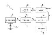
次ぎに、本発明を図に示す実施形態に基づいて詳細に説明する。図1に示すものは本発明に係る静電容量センサー回路1であり、この静電容量センサー回路1には測定側発振器2が設けられ、この測定側発振器2は接続された被測定容量3により周期が変化する発振器とされている。 Next, the present invention will be described in detail based on the embodiments shown in the drawings. FIG. 1 shows a
可変分周器4は制御信号に応じて分周数が変化する分周器、基準発振器5は一定の周期で発振する発振器、カウンター6は前記分周器4から出力される信号1周期の間に存在する基準発振器5からのパルス数をカウントするカウンター、増幅器7は任意の数Nrとカウンター6からの出力の差を増幅する回路、ループフィルター8は増幅器7からの高周波成分を減衰させるフィルターとする。The variable frequency divider 4 is a frequency divider whose frequency is changed according to a control signal, the
測定側発振器2の周期をT1、可変分周器4の分周数をN3とすると、可変分周器4の出力信号の周期T2は、
T2=T1×N3 …(1)
となる。基準発振器5の周期をT3とし、カウンター6が期間T2における基準発振器5のパルス数をカウントするものとすると、カウンター6の出力N4は、
N4=(T2/T3)=((T1×N3)/T3)…(2)
となる。増幅器7のゲインをA1とすると、増幅器の出力N5は、
N5=A1×(Nr−N4)=A1×(Nr−((T1×N3)/T3))…(3)When the period of the measurement-
T2 = T1 × N3 (1)
It becomes. Assuming that the period of the
N4 = (T2 / T3 ) = ((T1 × N3 ) / T3 ) (2)
It becomes. When the gain of the
N 5 = A 1 × (N r -N 4) = A 1 × (N r - ((
ループフィルター8を低域通過フィルタと仮定し、その伝達関数H(s)を、
H(s)=(Po/(Po+s))…(4)
とすると、ループフィルタ8の出力N6は、
N6=N5×H(s)=A1×(Nr−((T1×N3)/T3))×(P0/(P0+s))…(5)Assuming that the
H (s) = (Po / (Po + s)) (4)
Then, the output N6 of the
N6 = N5 × H (s) = A1 × (Nr − ((T1 × N3 ) / T3 )) × (P0 / (P0 + s)) (5)
ここで、可変分周器4の分周数N3がループフィルタ8の出力N6に依存し、その分周数N3を、
N3=K×N6…(6)
で表せるとすると、式(5)及び式(6)により、この負帰還ループの式は次式となる。
N6=A1×(Nr−((T1×N3)/T3))×(P0/(P0+S))
=A1×(Nr−((T1×K×N6)/T3))×(P0/(P0+s))…(7)Here, the dividing number N3 of the variable frequency divider 4 is dependent on the output N6 of the
N3 = K × N6 (6)
Can be expressed by the following equation from Equation (5) and Equation (6).
N6 = A1 × (Nr − ((T1 × N3 ) / T3 )) × (P0 / (P0 + S))
= A 1 × (N r - ((
式(7)より、
N6=(A1×Nr×P0)/(P0(1+A1×K×(T1/T3)+S))…(8)From equation (7)
N6 = (A1 × Nr × P0 ) / (P0 (1 + A1 × K × (T1 / T3 ) + S)) (8)
式(6)および式(8)より、可変分周器7の分周数N3は、
N3=K×N6=((A1×K×P0)/(P0(1+A1×K×(T1/T3)+S)))×Nr
=((ω2)/(ω1+s))×Nr…(9)From Equation (6) and Equation (8), the frequency dividing number N3 of the
N3 = K × N6 = ((A1 × K × P0 ) / (P0 (1 + A1 × K × (T1 / T3 ) + S))) × Nr
= ((Ω2 ) / (ω1 + s)) × Nr (9)
ここで、
ω1=P0(1+A1×K×T1/T3)…(10)
ω2=A1×K×P0 …(11)
とする。here,
ω1 = P0 (1 + A1 × K × T1 / T3 ) (10)
ω2 = A1 × K × P0 (11)
And
N3の応答特性はω1を極とする低域通過フィルタとなるので、ステップ応答に対する時間tにおけるN3は次式で表すことができる。
N3(t)=N7+N8(1−exp(−ω1t))…(12)Since the response characteristic of N3 is a low-pass filter having a pole .omega.1, N3 at time t for the step response can be expressed by the following equation.
N3 (t) = N7 + N8 (1-exp (−ω1 t)) (12)
ここで、時間t=0において、測定側の発振器の周期T1が、T1→T1+ΔT1に変化した際の応答について考える。式(9)により、時間t=0における可変分周器7の分周数Nは次式となる。
N3(s=0,T1=T1)=((A1×K)/(1+A1×K×(T1/T3)))×Nr…(13)
同様に、時間t→∞における可変分周器7の分周波数N3は、
N3(s=0,T1=T1+ΔT1)=((A1×K)/(1+A1×K×((T1+ΔT1)/T3)))×Nr…(14)Here, at time t = 0, the period T1 of the measurement-side oscillator, consider the response at the time of changes inT 1 → T 1 + ΔT 1 . From equation (9), the frequency division number N of the
N3 (s = 0, T1 = T1 ) = ((A1 × K) / (1 + A1 × K × (T1 / T3 ))) × Nr (13)
Similarly, the frequency N3 of the
N3 (s = 0, T1 = T1 + ΔT1 ) = ((A1 × K) / (1 + A1 × K × ((T1 + ΔT1 ) / T3 ))) × Nr (14)
式(12),(13)および(14)により、
N3(t=0)=N7=((A1×K)/(1+A1×K×(T1/T3)))×Nr…(15)
N3(t→∞)=N7+N8=((A1×K)/(1+A1×K×((T1+ΔT1)/T3)))×Nr…(16)From equations (12), (13) and (14),
N3 (t = 0) = N7 = ((A1 × K) / (1 + A1 × K × (T1 / T3 ))) × Nr (15)
N3 (t → ∞) = N7 + N8 = ((A1 × K) / (1 + A1 × K × ((T1 + ΔT1 ) / T3 ))) × Nr (16)
ここで、A1×K×(T1/T3)を>>1とすると、N7およびN8は、
N7=(T3/T1)×Nr…(17)
N8=N3(t→∞)−N7=(T3/(T1+ΔT1)-(T3/T1))×Nr…(18)Here, assuming that A1 × K × (T1 / T3 ) is >> 1, N7 and N8 are
N7 = (T3 / T1 ) × Nr (17)
N8 = N3 (t → ∞) −N7 = (T3 / (T1 + ΔT1 ) − (T3 / T1 )) × Nr (18)
式(12),(17)および(18)より、
N3(t)=N7+N8(1-exp(-ω1t))=((T3/T1+ΔT1)−((T3/(T1+ΔT1)−(T3/T1))×exp(-ω1t)))×Nr…(19)From equations (12), (17) and (18),
N3 (t) = N7 + N8 (1-exp (−ω1 t)) = ((T3 / T1 + ΔT1 ) − ((T3 / (T1 + ΔT1 ) − (T3 / T1 )) × exp (-ω1 t))) × Nr (19)
式(2)および式(19)によりN4は、
N4=「N3」(t)×(T1+ΔT1)/T3=Nr(1+(ΔT1/T1)×exp(-ω1t))…(20)
ここで、被測定容量「3」の容量をC3とし、その容量C3に対する測定用発振器5の周期T1が、
T(C3)=C3・R…(21)
となる特性であるとする。N4 is expressed by the following equations (2) and (19).
N4 = “N3 ” (t) × (T1 + ΔT1 ) / T3 = Nr (1+ (ΔT1 / T1 ) × exp (−ω1 t)) (20)
Here, the capacity of the capacity to be measured “3” is C3, and the period T1 of the
T (C3 ) = C3 · R (21)
It is assumed that the characteristics are as follows.
ここで、容量がC3→C3+ΔC3に変化することにより前記測定側発振器の周期T1がT1→T1+ΔT1に変化するものとすると、式(20)および(21)によりN4は、
N4=Nr(1+(ΔC3/C3)exp(-ω1t))となり、従って、N4は図2に示すような応答特性となり、N4を測定することにより容量の変化量ΔC3を求めることができる。Here, assuming that the period T1 of the measurement-side oscillator changes from T1 → T1 + ΔT1 by changing the capacitance from C3 → C3 + ΔC3 , N in accordance with equations (20) and (21)4 is
N4 = Nr (1+ (ΔC3 / C3 ) exp (−ω1 t)), and therefore N4 has a response characteristic as shown in FIG. 2, and the amount of change in capacitance by measuring N4 ΔC3 can be determined.
ここで、Nrは任意に設定された数であるので、被測定容量「3」の変化量に対する感度は被測定容量「3」の容量C3に依存することとなる。従って、基準側発振器の精度に依存しないので、基準側発振器に回路が測定用発振器と対称でなくとも、感度のバラツキは発生しない。Here, since Nr is an arbitrarily set number, the sensitivity to the amount of change of the measured capacitance “3” depends on the capacitance C3 of the measured capacitance “3”. Therefore, since it does not depend on the accuracy of the reference-side oscillator, even if the circuit on the reference-side oscillator is not symmetrical with the measurement oscillator, there is no sensitivity variation.
この構成を簡潔なデジタル回路で実現する際の例を図3に示す。この構成では、増幅器「7」にかわり、N4<Nrでは分周数を増加、N4=Nrでは分周数を維持、N4>Nrでは分周数を減少させる信号を出力させる比較器9とし、前の実施形態におけるループフィルタ8としては、任意の期間における前記比較器9からの出力を平均化する平均化回路10とする。この構成では前記ループフィルター8の入出力が3値で良いので、回路の小型化ができる。An example of realizing this configuration with a simple digital circuit is shown in FIG. In this configuration, instead of the amplifier “7”, a signal that increases the frequency division number when N4 <Nr , maintains the frequency division number when N4 = Nr , and outputs a signal that decreases the frequency number when N4 > Nr is output. It is assumed that the
1…静電容量検出回路
2…測定側発振器
3…被測定容量
4…可変分周器
5…基準発振器
6…カウンター
7…増幅器
8…ループフィルター
9…比較器
10…平均化回路DESCRIPTION OF
Claims (1)
Translated fromJapanesePriority Applications (1)
| Application Number | Priority Date | Filing Date | Title |
|---|---|---|---|
| JP2007166451AJP5150148B2 (en) | 2007-06-25 | 2007-06-25 | Capacitance detection circuit |
Applications Claiming Priority (1)
| Application Number | Priority Date | Filing Date | Title |
|---|---|---|---|
| JP2007166451AJP5150148B2 (en) | 2007-06-25 | 2007-06-25 | Capacitance detection circuit |
Publications (2)
| Publication Number | Publication Date |
|---|---|
| JP2009005259A JP2009005259A (en) | 2009-01-08 |
| JP5150148B2true JP5150148B2 (en) | 2013-02-20 |
Family
ID=40321123
Family Applications (1)
| Application Number | Title | Priority Date | Filing Date |
|---|---|---|---|
| JP2007166451AExpired - Fee RelatedJP5150148B2 (en) | 2007-06-25 | 2007-06-25 | Capacitance detection circuit |
Country Status (1)
| Country | Link |
|---|---|
| JP (1) | JP5150148B2 (en) |
Families Citing this family (2)
| Publication number | Priority date | Publication date | Assignee | Title |
|---|---|---|---|---|
| WO2010095074A1 (en) | 2009-02-17 | 2010-08-26 | Koninklijke Philips Electronics N.V. | Combining 3d image and graphical data |
| JP5444580B2 (en)* | 2009-07-15 | 2014-03-19 | 住友電工プリントサーキット株式会社 | Electrostatic sensor, flexible printed wiring board, and electronic device |
Family Cites Families (7)
| Publication number | Priority date | Publication date | Assignee | Title |
|---|---|---|---|---|
| JPS61104221U (en)* | 1984-12-14 | 1986-07-02 | ||
| JPH0590936A (en)* | 1991-09-30 | 1993-04-09 | Jiyaruko:Kk | Proximity detector using pll circuit for object |
| JPH0758635A (en)* | 1993-08-18 | 1995-03-03 | Kanebo Ltd | Frequency synthesizer |
| JP2002084179A (en)* | 2000-09-11 | 2002-03-22 | Gunze Ltd | Electrostatic capacity type proximity switch |
| JP2003043156A (en)* | 2001-07-31 | 2003-02-13 | Hideo Goto | Approach detecting method of object |
| JP2006344554A (en)* | 2005-06-10 | 2006-12-21 | Stanley Electric Co Ltd | Capacitance type door touch sensor |
| JP4687882B2 (en)* | 2005-07-29 | 2011-05-25 | スタンレー電気株式会社 | Capacitive lock switch |
- 2007
- 2007-06-25JPJP2007166451Apatent/JP5150148B2/ennot_activeExpired - Fee Related
Also Published As
| Publication number | Publication date |
|---|---|
| JP2009005259A (en) | 2009-01-08 |
Similar Documents
| Publication | Publication Date | Title |
|---|---|---|
| US9244104B2 (en) | Detecting a dielectric article | |
| KR101488008B1 (en) | Control circuit and control method for touch panel | |
| KR101697975B1 (en) | Inductive Displacement Sensor Using Frequency Modulation | |
| CN103339860B (en) | Capacitive proximity sensor and method for capacitive proximity detection | |
| US8613222B2 (en) | Detector, physical quantity measuring device, and electronic apparatus | |
| US11075634B2 (en) | Switching operation sensing apparatus with touch input member identification | |
| CA2196957A1 (en) | Electromagnetic-noise protection circuit | |
| US11320941B2 (en) | Sensing device with fingerprint sensor | |
| KR20180055294A (en) | FBAR Oscillator and Gas Sensing System using the FBAR Oscillator | |
| EP1424562A1 (en) | Sensor capacity sensing apparatus and sensor capacity sensing method | |
| US11003280B2 (en) | Switching operation sensing apparatus with low-power dual-sensing structure | |
| JP5150148B2 (en) | Capacitance detection circuit | |
| KR102185046B1 (en) | Switching operatiion sensing apparatus capable of identifying a touch object, and electronic devices | |
| US10254177B2 (en) | Temperature-to-digital converter | |
| CA2784085A1 (en) | Capacitive measuring circuit insensitive to high-frequency interference | |
| RU2397498C1 (en) | Compensation accelerometre | |
| JP2014006211A (en) | Sensor circuit | |
| US8593130B2 (en) | Detector, physical quantity measuring device, and electronic apparatus | |
| JP6718284B2 (en) | Signal processing circuit, coulomb counter circuit, electronic device | |
| US10578461B2 (en) | Capacitive sensor readout circuit | |
| JP2002090401A (en) | Capacitance sensor circuit | |
| US11360234B2 (en) | Electrode device, semiconductor device, and semiconductor system | |
| JP2007232711A (en) | Approach sensor device | |
| KR101168718B1 (en) | Apparatus and Method for Detection of Capacitance | |
| JP4207747B2 (en) | Capacitance type sensor and capacitance type distance measuring device |
Legal Events
| Date | Code | Title | Description |
|---|---|---|---|
| A621 | Written request for application examination | Free format text:JAPANESE INTERMEDIATE CODE: A621 Effective date:20100608 | |
| A977 | Report on retrieval | Free format text:JAPANESE INTERMEDIATE CODE: A971007 Effective date:20120319 | |
| A131 | Notification of reasons for refusal | Free format text:JAPANESE INTERMEDIATE CODE: A131 Effective date:20120501 | |
| A521 | Request for written amendment filed | Free format text:JAPANESE INTERMEDIATE CODE: A523 Effective date:20120618 | |
| TRDD | Decision of grant or rejection written | ||
| A01 | Written decision to grant a patent or to grant a registration (utility model) | Free format text:JAPANESE INTERMEDIATE CODE: A01 Effective date:20121106 | |
| A61 | First payment of annual fees (during grant procedure) | Free format text:JAPANESE INTERMEDIATE CODE: A61 Effective date:20121203 | |
| R150 | Certificate of patent or registration of utility model | Free format text:JAPANESE INTERMEDIATE CODE: R150 Ref document number:5150148 Country of ref document:JP Free format text:JAPANESE INTERMEDIATE CODE: R150 | |
| FPAY | Renewal fee payment (event date is renewal date of database) | Free format text:PAYMENT UNTIL: 20151207 Year of fee payment:3 | |
| R250 | Receipt of annual fees | Free format text:JAPANESE INTERMEDIATE CODE: R250 | |
| R250 | Receipt of annual fees | Free format text:JAPANESE INTERMEDIATE CODE: R250 | |
| R250 | Receipt of annual fees | Free format text:JAPANESE INTERMEDIATE CODE: R250 | |
| R250 | Receipt of annual fees | Free format text:JAPANESE INTERMEDIATE CODE: R250 | |
| R250 | Receipt of annual fees | Free format text:JAPANESE INTERMEDIATE CODE: R250 | |
| R250 | Receipt of annual fees | Free format text:JAPANESE INTERMEDIATE CODE: R250 | |
| R250 | Receipt of annual fees | Free format text:JAPANESE INTERMEDIATE CODE: R250 | |
| R250 | Receipt of annual fees | Free format text:JAPANESE INTERMEDIATE CODE: R250 | |
| LAPS | Cancellation because of no payment of annual fees |