JP5147491B2 - Acceleration sensor device - Google Patents
Acceleration sensor deviceDownload PDFInfo
- Publication number
- JP5147491B2 JP5147491B2JP2008086818AJP2008086818AJP5147491B2JP 5147491 B2JP5147491 B2JP 5147491B2JP 2008086818 AJP2008086818 AJP 2008086818AJP 2008086818 AJP2008086818 AJP 2008086818AJP 5147491 B2JP5147491 B2JP 5147491B2
- Authority
- JP
- Japan
- Prior art keywords
- acceleration sensor
- stopper plate
- pedestal
- sensor device
- weight portion
- Prior art date
- Legal status (The legal status is an assumption and is not a legal conclusion. Google has not performed a legal analysis and makes no representation as to the accuracy of the status listed.)
- Expired - Fee Related
Links
Images


Classifications
- G—PHYSICS
- G01—MEASURING; TESTING
- G01P—MEASURING LINEAR OR ANGULAR SPEED, ACCELERATION, DECELERATION, OR SHOCK; INDICATING PRESENCE, ABSENCE, OR DIRECTION, OF MOVEMENT
- G01P15/00—Measuring acceleration; Measuring deceleration; Measuring shock, i.e. sudden change of acceleration
- G01P15/02—Measuring acceleration; Measuring deceleration; Measuring shock, i.e. sudden change of acceleration by making use of inertia forces using solid seismic masses
- G01P15/08—Measuring acceleration; Measuring deceleration; Measuring shock, i.e. sudden change of acceleration by making use of inertia forces using solid seismic masses with conversion into electric or magnetic values
- G01P15/12—Measuring acceleration; Measuring deceleration; Measuring shock, i.e. sudden change of acceleration by making use of inertia forces using solid seismic masses with conversion into electric or magnetic values by alteration of electrical resistance
- G01P15/123—Measuring acceleration; Measuring deceleration; Measuring shock, i.e. sudden change of acceleration by making use of inertia forces using solid seismic masses with conversion into electric or magnetic values by alteration of electrical resistance by piezo-resistive elements, e.g. semiconductor strain gauges
- G—PHYSICS
- G01—MEASURING; TESTING
- G01P—MEASURING LINEAR OR ANGULAR SPEED, ACCELERATION, DECELERATION, OR SHOCK; INDICATING PRESENCE, ABSENCE, OR DIRECTION, OF MOVEMENT
- G01P15/00—Measuring acceleration; Measuring deceleration; Measuring shock, i.e. sudden change of acceleration
- G01P15/02—Measuring acceleration; Measuring deceleration; Measuring shock, i.e. sudden change of acceleration by making use of inertia forces using solid seismic masses
- G01P15/08—Measuring acceleration; Measuring deceleration; Measuring shock, i.e. sudden change of acceleration by making use of inertia forces using solid seismic masses with conversion into electric or magnetic values
- G01P15/0802—Details
- G—PHYSICS
- G01—MEASURING; TESTING
- G01P—MEASURING LINEAR OR ANGULAR SPEED, ACCELERATION, DECELERATION, OR SHOCK; INDICATING PRESENCE, ABSENCE, OR DIRECTION, OF MOVEMENT
- G01P15/00—Measuring acceleration; Measuring deceleration; Measuring shock, i.e. sudden change of acceleration
- G01P15/18—Measuring acceleration; Measuring deceleration; Measuring shock, i.e. sudden change of acceleration in two or more dimensions
- G—PHYSICS
- G01—MEASURING; TESTING
- G01P—MEASURING LINEAR OR ANGULAR SPEED, ACCELERATION, DECELERATION, OR SHOCK; INDICATING PRESENCE, ABSENCE, OR DIRECTION, OF MOVEMENT
- G01P15/00—Measuring acceleration; Measuring deceleration; Measuring shock, i.e. sudden change of acceleration
- G01P15/02—Measuring acceleration; Measuring deceleration; Measuring shock, i.e. sudden change of acceleration by making use of inertia forces using solid seismic masses
- G01P15/08—Measuring acceleration; Measuring deceleration; Measuring shock, i.e. sudden change of acceleration by making use of inertia forces using solid seismic masses with conversion into electric or magnetic values
- G01P2015/0805—Measuring acceleration; Measuring deceleration; Measuring shock, i.e. sudden change of acceleration by making use of inertia forces using solid seismic masses with conversion into electric or magnetic values being provided with a particular type of spring-mass-system for defining the displacement of a seismic mass due to an external acceleration
- G01P2015/0822—Measuring acceleration; Measuring deceleration; Measuring shock, i.e. sudden change of acceleration by making use of inertia forces using solid seismic masses with conversion into electric or magnetic values being provided with a particular type of spring-mass-system for defining the displacement of a seismic mass due to an external acceleration for defining out-of-plane movement of the mass
- G01P2015/084—Measuring acceleration; Measuring deceleration; Measuring shock, i.e. sudden change of acceleration by making use of inertia forces using solid seismic masses with conversion into electric or magnetic values being provided with a particular type of spring-mass-system for defining the displacement of a seismic mass due to an external acceleration for defining out-of-plane movement of the mass the mass being suspended at more than one of its sides, e.g. membrane-type suspension, so as to permit multi-axis movement of the mass
- G01P2015/0842—Measuring acceleration; Measuring deceleration; Measuring shock, i.e. sudden change of acceleration by making use of inertia forces using solid seismic masses with conversion into electric or magnetic values being provided with a particular type of spring-mass-system for defining the displacement of a seismic mass due to an external acceleration for defining out-of-plane movement of the mass the mass being suspended at more than one of its sides, e.g. membrane-type suspension, so as to permit multi-axis movement of the mass the mass being of clover leaf shape
Landscapes
- Physics & Mathematics (AREA)
- General Physics & Mathematics (AREA)
- Pressure Sensors (AREA)
Description
Translated fromJapanese本発明は、加速度を検出する加速度センサ装置、特に半導体微細加工プロセスにより形成されるMEMS(Microelectromechanical System)技術を用いた加速度センサ装置に関するものである。 The present invention relates to an acceleration sensor device for detecting acceleration, and more particularly to an acceleration sensor device using MEMS (Microelectromechanical System) technology formed by a semiconductor micromachining process.
従来、MEMS技術を用いた片手持ち型構造や両手持ち型構造の加速度センサ装置が、例えば、次のような文献等に開示されている。 Conventionally, an acceleration sensor device having a one-handed structure or a two-handed structure using the MEMS technology has been disclosed in, for example, the following documents.
特許文献1には、両手持ち型構造のピエゾ抵抗型3軸加速度センサ装置の技術が開示されている。このピエゾ抵抗型3軸加速度センサ装置は、薄いシリコンの梁部(ビーム)によって錘部を両側から支え、加速度によって錘部が動くことで梁部が歪み、この歪みを、梁部内に形成したピエゾ抵抗素子の抵抗変化で加速度を検出するMEMS加速度センサチップを有している。更に、錘部の過度な上方への変位を規制するために、錘部上に所定間隔隔ててストッパ板が設けられている。そして、このような加速度センサチップ及びストッパ板が中空のパッケージ内に収納されている。
特許文献2には、片手持ち型構造のピエゾ抵抗型加速度センサ装置の技術が開示されている。このピエゾ抵抗型加速度センサ装置は、シリコンの梁部によって錘部を片側から支え、加速度によって錘部が上下に変位することで錘部が歪み、この歪みを、梁部上に形成したピエゾ抵抗素子の抵抗変化で加速度を検出するMEMS加速度センサチップを有している。更に、錘部の上下の変位を規制するために、この錘部の上下に所定間隔隔ててストッパ基板が設けられている。
特許文献3には、片手持ち型構造のピエゾ抵抗型加速度センサ装置の技術が開示されている。このピエゾ抵抗型加速度センサ装置は、シリコンの梁部によって錘部を片側から支え、加速度によって錘部が上下に変位することで錘部が歪み、この歪みを、梁部上に形成したピエゾ抵抗素子の抵抗変化で加速度を検出するMEMS加速度センサチップを有している。錘部の上下の変位を規制するために、この錘部上には、所定間隔隔てて線状のストッパが設けられている。更に、錘部の下には、所定間隔隔てた凹所を有するカバーが配置され、その凹所内に、錘部の下方向の変位を規制する突起状のストッパが形成されている。
しかしながら、従来の加速度センサ装置では、次のような課題があった。
特許文献1に開示された両手持ち型構造の加速度センサ装置では、複数の梁部を有しており、加速度を検出する時に錘部が変位することで、その梁部が上方へ撓むことがある。この時、ストッパ板によって錘部の変位を制限しようとする場合、変位の調整(MEMS加速度センサチップとストッパ板との間隔による調整)によっては、梁部がストッパ板に衝突し、その衝突した梁部が破損する場合がある。However, the conventional acceleration sensor device has the following problems.
The acceleration sensor device having a two-handed structure disclosed in
又、特許文献1のようなピエゾ抵抗型加速度センサ装置では、ピエゾ抵抗素子形成近傍の梁部とストッパ板とが衝突する場合があり、ピエゾ抵抗素子そのもの、及び、その表面に形成された保護膜に損傷を及ぼすことがある。ピエゾ抵抗素子そのものはもとより、その表面の保護膜の損傷により、ピエゾ抵抗素子にかかる応力に変化が生じ、ピエゾ抵抗素子の特性が変化する虞がある。 Further, in the piezoresistive acceleration sensor device as in
なお、特許文献2、3に開示された片手持ち型構造の加速度センサ装置では、錘部の梁部に接続される部分の反対側が開放された状態であるため、この反対側の部分が梁部の撓み以上に変位するので、梁部がストッパ基板あるいは線状のストッパに衝突する事態が招来しない。 In addition, in the acceleration sensor device having a one-hand-held structure disclosed in
本発明の加速度センサ装置は、錘部、前記錘部の周囲に離間して配置された台座部、及び、前記錘部と前記台座部とを可撓的に接続する複数の梁部を有する加速度センサチップと、前記加速度センサチップ上に設けられるストッパ板とを備え、前記ストッパ板は、前記台座部に対向する位置に突設され、接着剤により前記台座部に接着される複数の固定部と、前記各固定部の周辺であって前記錘部に対向する位置にそれぞれ形成され、前記錘部の変位を規制する第1の凹部と、前記梁部に対向する位置に形成され、前記第1の凹部よりも深い第2の凹部とを有している。そして、前記複数の固定部における前記台座部に対向する面には、同一方向に延びる接着剤充填用の複数の第1のスリットがそれぞれ形成され、前記複数の固定部に形成された前記第1のスリットは互いに同一の方向に延在している。An acceleration sensor device according to the present invention includes a weight portion, a pedestal portion that is spaced apart from the periphery of the weight portion, and aplurality of beam portions that flexibly connect the weight portion and the pedestal portion. a sensor chip, and a stopper plate provided on the acceleration sensor chip, the stopper plate is projected at a position opposed to the base portion, and a plurality of fixing portions which arebonded to the base portionby an adhesive A first recess formed around each of the fixed portions and facing the weight portion; a first recess for restricting the displacement of the weight portion; and a position facing the beam portion;and have a deep second recess than the recessof. A plurality of first slits for filling an adhesive extending in the same direction are respectively formed on a surface of the plurality of fixing portions facing the pedestal portion, and the first slit formed in the plurality of fixing portions. The slits extend in the same direction.
本発明の他の加速度センサ装置は、錘部、前記錘部の周囲に離間して配置された台座部、及び、前記錘部と前記台座部とを可撓的に接続する複数の梁部を有する加速度センサチップと、前記加速度センサチップ上に設けられるストッパ板とを備え、前記ストッパ板は、前記錘部に対して所定の間隔をもって接着剤により前記台座部に接着され、前記錘部の変位を規制する固定部と、前記固定部における前記梁部に対向する位置に形成された凹部とを有している。そして、前記固定部における前記台座部に対向する箇所には、同一方向に延びる接着剤充填用の複数の第1のスリットが形成されている。Another acceleration sensor device according to the present invention includes a weight portion, a pedestal portion that is spaced apart from the periphery of the weight portion, and aplurality of beam portions that flexibly connect the weight portion and the pedestal portion. an acceleration sensor chip having, and a stopper plate provided on the acceleration sensor chip, the stopper plate isbonded to the base portionby an adhesive with a predetermined gap with respect to the weight portion, the displacement of the weight portionand possess a fixing portion for regulating the and a recess formed at a position opposed to the beam portion of the fixingunit. And the some 1st slit for the adhesive filling extended in the same direction is formed in the location which opposes the said base part in the said fixing | fixed part.
本発明によれば、ストッパ板における梁部に対応する位置に凹部が形成されているので、梁部に衝撃を与えることなく錘部の変位を制限することが可能となる。更に、固定部に複数の第1のスリットが同一方向に形成されているので、台座部上に塗布された余分な接着剤を同一方向へ逃がすことができる。According to the present invention, since the concave portionis formed at a position corresponding to the beam portion in the stopper plate, the displacement of the weight portion can be limited without giving an impact tothe beam portion.Further, since the plurality of first slits are formed in the same direction in the fixing portion, it is possible to release the excess adhesive applied on the pedestal portion in the same direction.
本発明を実施するための最良の形態は、以下の好ましい実施例の説明を添付図面と照らし合わせて読むと、明らかになるであろう。但し、図面はもっぱら解説のためのものであって、本発明の範囲を限定するものではない。 The best mode for carrying out the invention will become apparent from the following description of the preferred embodiments when read in conjunction with the accompanying drawings. However, the drawings are only for explanation and do not limit the scope of the present invention.
(実施例1の構成)
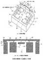
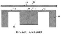
図1(a)、(b)は、本発明の実施例1における両手持ち型構造のピエゾ抵抗型3軸加速度センサ装置を示す概略の構成図であり、同図(a)は模式的な全体斜視図、及び、同図(b)は同図(a)中のA1−A2線拡大端面図である。図2は図1(a)中のB1−B2線拡大端面図、図3は図1中の加速度センサチップを示す平面図、図4は図1中のストッパ板を示す底面図、及び、図5は図1中の加速度センサチップ上にストッパ板が搭載された状態を示す平面図である。なお、図1(a)中のA1−A2線の切断箇所に対応する切断箇所が、図4中にも同符号のA1−A2線として示されている。(Configuration of Example 1)
FIGS. 1A and 1B are schematic configuration diagrams showing a piezoresistive three-axis acceleration sensor device having a two-handed structure in Example 1 of the present invention. FIG. 1A is a schematic overall view. The perspective view and FIG. 7B are enlarged views of the A1-A2 line in FIG. 2 is an enlarged end view taken along line B1-B2 in FIG. 1A, FIG. 3 is a plan view showing the acceleration sensor chip in FIG. 1, FIG. 4 is a bottom view showing the stopper plate in FIG. 5 is a plan view showing a state in which a stopper plate is mounted on the acceleration sensor chip in FIG. In addition, the cutting location corresponding to the cutting location of the A1-A2 line in Fig.1 (a) is also shown as the A1-A2 line of the same code | symbol in FIG.
図1及び図2に示す加速度センサ装置は、例えば、MEMS技術を用いてSOI(Silicon on Insulator)基板等を微細加工して形成された加速度センサチップ10と、シリコン基板等にエッチング等の処理を施して形成され、その加速度センサチップ10上に固着される蓋状のストッパ板20とを備えている。 The acceleration sensor device shown in FIGS. 1 and 2 includes, for example, an
加速度センサチップ10は、図1〜図3に示されるように、例えば、上面が方形状であって、全体がほぼ四角柱(X軸方向の縦1.7±0.5mm、Y軸方向の横1.7±0.5mm、Z軸方向の厚さ350±50μm程度)をなし、中央に配置された錘部11と、この錘部11の周囲に離間して配置された台座部12と、この台座部12に対して直交するX軸及びY軸方向の4箇所から揺動自在(可撓的)に錘部11を支持する梁部13とを有している。 As shown in FIGS. 1 to 3, the
錘部11は、Z軸方向の上下の変位が可能なように、台座部12の厚みよりも薄くなっており、中心に配置された、上面が方形状であって、ほぼ四角柱の中心質量部11aと、この中心質量部11aの四隅に接続された、上面が方形状であって、ほぼ四角柱の4つの周辺質量部11bとにより構成されている。各周辺質量部11bの周囲には、この周辺質量部11bの横方向(即ち、X軸及びY軸を含む平面方向)の変位が可能なように、スリット14がそれぞれ形成され、このスリット14を介して、錘部11の周囲が台座部12によって囲まれている。台座部12と中心質量部11aとは、直交するX軸及びY軸方向に配置された帯状の4つの梁部13により可撓的に接続されている。 The
各梁部13の平面(即ち、上面)内には、複数のピエゾ抵抗素子15がそれぞれ形成されている。更に、台座部12の上面の両側部上には、外部引き出し端子用の複数のパッド16がX軸方向にそれぞれ形成されている。複数のピエゾ抵抗素子15は、X軸、Y軸、Z軸のそれぞれの加速度を検出するブリッジ回路を構成するように、図示しない配線層を介して、複数のバッド16に電気的に接続されている。これらのパッド16を除く加速度センサチップ10の上面は、シリコン窒化膜等の保護膜により被覆されている。 A plurality of
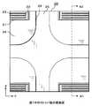
ストッパ板20は、図1、図2及び図4に示されるように、加速度センサチップ10上に接着剤(ダイスボンド)30により固着される方形状の板(例えば、シリコン板)であり、平面(即ち、表面)が平らになっている。ストッパ板20の表面サイズは、加速度センサチップ10よりも少し大きめで、例えば、X軸方向の縦1.5±0.5mm、Y軸方向の横2.0±0.5mm、及び、Z軸方向の厚さ90±20μm程度であり、図5に示されるように、Y軸の右側に少しはみ出して加速度センサチップ10上に搭載される。なお、ストッパ板20の表面サイズは、加速度センサチップ10の上面サイズと同一か、又は小さくてもよい。 The
ストッパ板20の底面(即ち、裏面)において、台座部上面の四隅に対向する四隅の位置に、接着剤30により台座部12に固着するための4つの固定部21が突設されている。ここで、ストッパ板20は、加速度センサチップ10の錘部11及び梁部13を覆うストッパ部としての機能を有し、更に、接着剤30は、加速度センサチップ10の台座部12と前記ストッパ部とを接続する接着層としての機能を有している。各固定部21は、底面が方形であり、厚さが例えば5±0.5μm程度である。この各固定部21の底面には、同一方向(例えば、Y軸方向)に延びる接着剤充填用の複数の第1のスリット22がそれぞれ形成されている。各スリット22の幅、及び各スリット間隔は、例えば、40±5μm程度である。4つの固定部21にそれぞれ形成される複数の第1のスリット22は、すべて同一方向に延在しており、塗布される接着剤30を受け入れて余分な接着剤30を同一方向へ逃がす溝の機能を有している。更に、複数の第1のスリット22の梁部13側の端部に接続され、このスリット22に対してほぼ垂直方向(例えば、X軸方向)に延在する、接着剤はみ出し防止用の第2のスリット23がそれぞれ形成されている。 On the bottom surface (i.e., the back surface) of the
4つの各固定部21の周辺であって錘部11の周辺質量部11bに対向する位置には、周辺質量部11bにおけるZ軸の上方への変位を規制する第1の凹部24がそれぞれ形成され、更に、この4つの第1の凹部24に隣接して、4つの梁部13に対向する位置に、第1の凹部24よりも深い第2の凹部25が形成されている。例えば、第1の凹部24の深さは固定部底面から5±0.5μm程度、第2の凹部25の深さは第1の凹部底面から5±0.5μm程度である。 A
各第1の凹部24と第2の凹部25との境界26は、図4及び図5に示すように、その一部が曲線形状になっている。即ち、第2の凹部25は、ストッパ板裏面において梁部13に対向する位置に所定の幅を有するほぼ十字形に形成され、この十字形の中央部分と各第1の凹部24との境界26が、錘部11を構成する周辺質量部11bの一部を通る曲線形状になっている。上面から見た場合のこの曲線形状は、周辺質量部11bにおける中央質量部11aから最も離れた角部に隣接した二つの角部近傍に対応する位置を通る曲線であって、中央質量部11a側に突出する弧状になっている。又、十字形の端部の幅は、隣接する周辺質量部11bの間隔よりも広く設けられている。かかる形状によって境界26は構成されている。 As shown in FIGS. 4 and 5, a part of the
従って、第1の凹部24及び第2の凹部25がこのような形状となるため、ストッパ板20と梁部13との距離がストッパ板20と錘部11の距離より大きい構成となる。更に、錘部11の中でも、周辺質量部11bにおける中央質量部11aから最も離れた角部とストッパ板20との距離が、この最も離れた角部に隣接する角部とストッパ板20との距離よりも小さい構成となる。 Therefore, since the
このように、上述のストッパ板20の形状及び加速度センサチップ10とストッパ板20との位置関係によって、ストッパ板20は梁部13との接触を防ぎ、加速度センサチップ10の特性の変動を防止することができる。更に、周辺質量部11bの一部を第1の凹部24が覆うため、錘部11との接触面積が過度に大きくなることを防止しつつ錘部11の変位を制御することが可能となる。 Thus, the
(実施例1の製造方法例)
(a) 加速度センサチップ10の製造方法
図1及び図2に示す加速度センサチップ10は、例えば、MEMS技術を用いてSOIウェハをホトリソエッチング等により微細加工して多数形成した後、個々の加速度センサチップに分割されて形成される。(Example of production method of Example 1)
(A) Manufacturing Method of
(b) ストッパ板20の製造方法
図6(1)〜(7)は、図4のストッパ板20中のA1−A2線の切断箇所の製造方法例を示す概略の製造工程図である。(B) Manufacturing Method of
例えば、シリコンウェハに配置される多数の方形状のストッパ板形成領域(X軸方向の縦1.5±0.5mm、Y軸方向の横2.0±0.5mm、及び、Z軸方向の厚さ(T1)625μm±20μm程度)において、そのシリコンウェハを構成するシリコン基板30上に、レジストを形成し、図4の第2の凹部25に対応する領域31aを除去して第1のレジストパタン31を選択的に形成する(図6(1)の工程)。 For example, a large number of rectangular stopper plate formation regions (1.5 ± 0.5 mm in the X-axis direction, 2.0 ± 0.5 mm in the Y-axis direction, and Z-axis direction) arranged on the silicon wafer In the thickness (T1) of about 625 μm ± 20 μm, a resist is formed on the
ドライエッチングにより、第1のレジストパタン31をマスクにしてシリコン基板30の領域31aを除去してシリコン基板30上に凹部25aを形成し(図6(2)の工程)、その後、不必要になった第1のレジストパタン31を除去する(図6(3)の工程)。 By dry etching, the
次に、別途レジストを形成し、図4の第1の凹部24、第2の凹部25、固定部21中の第1のスリット22、及び第2のスリット23に対応する領域32aを除去した第2のレジストパタン32を選択的に形成する(図6(4)の工程)。なお、他の作製方法として、例えば、ポリイミド樹脂(集積回路(IC)の保護コートとして用いるコート剤)を用いてもよい。通常10μm程度でコートし、同じマスクを用いることによって、パターニング現像処理を行い、キュアすることにより5μm程度厚まで収縮し、同様の効果を得ることが可能となる。この他の作成方法では、ドライエッチングを使用しなくてもよい。 Next, a resist is separately formed, and the
ドライエッチングにより、第2のレジストパタン32をマスクにして、シリコン基板30における領域32aと凹部25aの領域とを均一に除去し、第1のスリット22及び第2のスリット23を有する固定部21と、第1の凹部24と、第2の凹部25とを形成し、(図6の(5)の工程)、その後、不必要になった第2のレジストパタン32を除去する(図6(6)の工程)。例えば、固定部21中の第1のスリット22の幅とスリット間隔は40±5μm程度、固定部21の表面から第1の凹部24までの段差(T2)は1.3μm〜10μm程度(好ましくは5±0.5μm程度)、及び、第1の凹部24から第2の凹部25までの段差(T3)は5±0.5μm程度である。 By dry etching, using the second resist
最後に、シリコン基板30の裏面側から研磨処理を施し、シリコンウェハを所望の厚み(例えば、Z軸方向の厚さ(T4)100μm±20μm程度)に調整する(図6(7)の工程)。このようにしてシリコンウェハに形成された多数のストッパ板20は、個々のストッパ板に分割される。 Finally, a polishing process is performed from the back side of the
(c) ストッパ板20の固定方法
搭載装置(ダイボンダー)に加速度センサチップ10を固定し、図5に示すように、台座部12上の四隅近傍に、接着剤30を所定量塗布する。接着剤30は、ストッパ板20の影響を台座部12へ伝え難くするために、シリコーン樹脂を主成分等にした柔らかい材料を用いることが望ましい。接着剤30を塗布するための台座部12上の四隅近傍の4箇所の位置は、塗布後の接着剤30の広がりを考慮して、接着剤塗布位置の左側は可能な限り台座部12側の梁部13から離す位置で、且つ、左列のパッド16側へも影響のない位置が望ましい。接着剤30の塗布量は、例えば、ばらつきを考慮に入れたときの塗布量の最大値で塗布された場合の接着剤体積を算出し、この接着剤体積が納まる第1及び第2のスリット22,23の溝容積等より設定することができる。(C) Fixing method of
ダイボンダーによりストッパ板20を把持し、このストッパ板20の裏面側を加速度センサチップ10上に位置決めする。この位置決めでは、例えば、左側の接着剤塗布位置に合わせてストッパ板20側の固定部21を合わせる等して、ストッパ板20におけるほぼ十字形の第2の凹部25の中心点と、錘部11における中心質量部11aの中心点とを一致させる。これにより、図5において、ストッパ板20の左辺が、台座部12側の左辺のパッド16列から右方向へずれ、ストッパ板20の右辺が、台座部12側の右辺からはみ出し、更に、ストッパ板20の上辺及び下辺が、台座部12側の上辺及び下辺から少しはみ出した状態になる。 The
ストッパ板20を位置決めした後、このストッパ板20を加速度センサチップ10上に載置し、上からストッパ板20に所定の加重を加えて所定時間加熱処理(ベーク)する。すると、各固定部21に形成された接着剤30の流れ止め用の複数の第1のスリット22が全て同じY軸方向に延在しているので、塗布された接着剤30の内の余分な接着剤30が一定のY軸方向に逃れ、この結果、接着剤30の応力を一定のY軸方向のみに逃すことができ、X軸方向は勿論、Y軸方向に掛かる力のバランスも取りやすくなり、加速度センサチップ10の歪み(即ち、出力変動)を抑制することが可能になる。又、各固定部21にはX軸方向に第2のスリット23が形成されているので、塗布された接着剤30の梁部13側へのはみ出しを防止できる。 After positioning the
所定時間の加圧及び加熱処理を行うと、加速度センサチップ10側の台座部12上に、所定の厚みの接着剤30を介して、ストッパ板20の裏面側の固定部21が固定され、加速度センサチップ10の製造が終了する。 When pressurization and heat treatment are performed for a predetermined time, the fixing
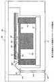
(d) パッケージへの組立方法
図7は、図1の加速度センサ装置におけるパッケージへの搭載例を示す概略の断面図である。(D) Method of assembling into package FIG. 7 is a schematic cross-sectional view showing an example of mounting in the package in the acceleration sensor device of FIG.
加速度センサ装置を搭載するためのパッケージ40は、例えば、上端が開口した中空のパッケージ本体41を有し、このパッケージ本体41内の段差部42に複数のパッド43が形成されている。複数のパッド43は、パッケージ本体41内を上下方向に貫通する導電性のビアホール44を介して、パッケージ本体41の底面に設けられた外部端子45に対して電気的に接続されている。パッケージ本体41の上端の開口部は、蓋46により封止される。 The
このようなパッケージ40内に図1の加速度センサ装置を搭載する場合は、ストッパ板20が固着された台座部12の底面を、固定台47を介して、パッケージ本体40内の底面に接着剤等で固定する。この際、錘部11の厚みは台座部12の厚みよりも薄いので、錘部11の底面と固定台47との間には、錘部11の下方への変位を可能にする所定の間隙が形成される。台座部12の上面のパッド16とパッケージ本体41側のパッド43とをワイヤ47で接続する。その後、パッケージ本体41の上端の開口部を蓋46により封止すれば、組立が終了する。 When the acceleration sensor device of FIG. 1 is mounted in such a
(実施例1の動作)
図7において、加速度センサチップ10に加速度が作用すると、加速度の方向及び大きさに応じて錘部11が台座部12に対して相対的に変位し、梁部13が撓んでピエゾ抵抗素子15の抵抗値が変化する。この抵抗値の変化を外部端子45から検出することにより、加速度センサチップ10に作用したX軸方向、Y軸方向、及びZ軸方向それぞれの加速度を検出することができる。(Operation of Example 1)
In FIG. 7, when acceleration acts on the
大きな加速度が作用して、錘部11がZ軸の上方へ過度に変位した場合は、錘部11における周辺質量部11bの上面の一部が、ストッパ板20の裏面側の第1の凹部24の底面に衝突して錘部11の上方への変位が規制される。 When a large acceleration is applied and the
(実施例1の効果)
本実施例1によれば、次の(i)、(ii)のような効果がある。(Effect of Example 1)
According to the first embodiment, there are the following effects (i) and (ii).
(i) 錘部11がZ軸の上方へ過度に変位した場合は、周辺質量部11bの上面の一部が第1の凹部24の底面に衝突して錘部11の上方への変位が規制され、第1の凹部24よりも深い第2の凹部25の底面には、梁部13が衝突しないので、この梁部13の破壊を防止でき、更に、梁部13内に形成されたピエゾ抵抗素子15も第2の凹部25の底面に衝突しないので、このピエゾ抵抗素子15の特性の変位も防止できる。 (I) When the
即ち、錘部11の上面における中心質量部11aの全部及び周辺質量部11bの一部を含むように広くほぼ十字形の第2の凹部25とすることで、一番変位量が大きいであろう梁部13と錘部11の中心質量部11aとの接続部、及びその中心質量部11aの近傍については衝突し難くすることにより、錘部11、梁部13及びピエゾ抵抗素子15の破損や特性変化を防止し、ひいては加速度センサ装置の信頼性を向上できる。 That is, the displacement amount will be the largest by forming the second
(ii) 図4及び図5に示すように、固定部21に複数の第1のスリット22が同一方向に形成されているので、台座部12上に塗布された余分な接着剤30を同一方向へ逃がすことができる。その上、ストッパ板20の裏面側において、第1の凹部24と第2の凹部25との境界26が曲面形状になっているので、第1の凹部24と錘部11の周辺質量部11bとの衝突時の衝撃が一点に集中し難くなり、破損し難くなる。又、第1の凹部24の底面と錘部11の周辺質量部11bとが接触すると、ストッパ板20の裏面に電荷が溜まり、ストッパ板20の静電引力により錘部11が引き上げられ、加速度センサチップ10の出力が変動する虞がある。しかし、境界26が曲面形状になっているので、第1の凹部24の底面と錘部11の周辺質量部11bとの接触面積が小さくなり、これにより発生する電荷量も小さくなって出力変動も抑制ができる。(Ii) As shown in FIGS. 4 and 5, theplurality of
図8は、本発明の実施例2における両手持ち型構造のピエゾ抵抗型3軸加速度センサ装置を示す概略の拡大端面図であり、実施例1を示す図1(b)中の要素と共通の要素には共通の符号が付されている。 FIG. 8 is a schematic enlarged end view showing a piezoresistive triaxial acceleration sensor device having a two-handed structure according to the second embodiment of the present invention, and is common to the elements in FIG. 1B showing the first embodiment. Elements are given common symbols.
本実施例2の加速度センサ装置では、実施例1のストッパ板20に代えて、これとは構成の異なるストッパ板20Aが、所定の厚みを有する接着剤30Aにより、実施例1と同様の加速度センサチップ10上に固着されている。接着剤30Aは、実施例1の接着剤30に比べて厚く塗布され、固定部21Aの裏面と加速度センサチップ10の上面との間の間隔が、実施例1の第1の凹部24の底面と加速度センサチップ10の上面との間の間隔とほぼ同一になるように設定されている。 In the acceleration sensor device according to the second embodiment, instead of the
本実施例2のストッパ板20Aは、平面側である表面が平らである。このストッパ板20Aの底面側である裏面には、加速度センサチップ10側の錘部11に対して所定の間隔をもって接着剤30Aにより台座部12に固着される錘部変位規制用の固定部21Aと、この固定部21Aにおける梁部13に対向する位置に形成された凹部25(これは実施例1の第2の凹部25と同一)とが設けられている。固定部21Aにおける台座部12の四隅近傍に対向する4箇所には、実施例1と同様に、同一のY軸方向に延びる接着剤充填用の複数の第1のスリット22がそれぞれ形成され、更に、この複数の第1のスリット22に対してほぼ垂直方向に接着剤はみ出し防止用の第2のスリット23がそれぞれ形成されている。 The
固定部21Aと凹部25との境界は、実施例1と同様に、曲面形状になっている。即ち、凹部25は、実施例1と同様に、ストッパ板20Aにおいて梁部13に対向する位置に所定の幅を有するほぼ十字形に形成され、この十字形の交叉箇所と固定部21Aとの境界が、錘部11の周辺質量部11bを通る曲面形状になっている。その他の構成は、実施例1と同様である。 The boundary between the fixed
このような構成の加速度センサ装置では、実施例1とほぼ同様の作用効果が得られる。特に、本実施例2の固定部21Aは、実施例1の第1の凹部24の領域まで形成されているので、ストッパ板20Aの製造工程の内の実施例1の第1の凹部24を形成するための工程を省略でき、製造工程を簡略化できる。 In the acceleration sensor device having such a configuration, substantially the same operational effects as those of the first embodiment can be obtained. Particularly, since the fixing
(変形例)
本発明は、上記実施例1、2に限定されず、加速度センサチップ10、ストッパ板20,20A、及びパッケージ40の構造、形状、サイズ、あるいは製造方法等は、図示以外の種々のものに変形可能である。例えば、図4に示す4つの固定部21の配置方向を変更し、X軸方向に延在する形状にしてもよく、これにより、上記実施例1、2とほぼ同様の作用効果が得られる。又、実施例1、2の加速度センサ装置を1軸又は2軸式の加速度センサ装置に変更したり、あるいは、片手持ち型構造に変更することも可能である。(Modification)
The present invention is not limited to the first and second embodiments, and the structure, shape, size, manufacturing method, and the like of the
10 加速度センサチップ
11 錘部
12 台座部
13 梁部
15 ピエゾ抵抗素子
20,20A ストッパ板
21、21A 固定部
22,23 スリット
24,25 凹部
30,30A 接着剤
40 パッケージDESCRIPTION OF
Claims (10)
Translated fromJapanese前記加速度センサチップ上に設けられるストッパ板とを備え、
前記ストッパ板は、
前記台座部に対向する位置に突設され、接着剤により前記台座部に接着される複数の固定部と、
前記各固定部の周辺であって前記錘部に対向する位置にそれぞれ形成され、前記錘部の変位を規制する第1の凹部と、
前記梁部に対向する位置に形成され、前記第1の凹部よりも深い第2の凹部とを有し、
前記複数の固定部における前記台座部に対向する面には、同一方向に延びる接着剤充填用の複数の第1のスリットがそれぞれ形成され、前記複数の固定部に形成された前記第1のスリットは互いに同一の方向に延在していることを特徴とする加速度センサ装置。An acceleration sensor chip having a weight portion, a pedestal portion disposed around the weight portion, and a plurality of beam portions that flexibly connect the weight portion and the pedestal portion;
A stopper plate provided on the acceleration sensor chip,
The stopper plate is
A plurality of fixing portions that are projected at a position facing the pedestal portion and bonded to the pedestal portion with an adhesive;
A first recess that is formed around each of the fixed portions and is opposed to the weight portion, and restricts displacement of the weight portion;
Formed at a position facing the beam portion, and having a second recess deeper than the first recess,
A plurality of first slits for filling an adhesive extending in the same direction are formed on a surface of the plurality of fixing portions facing the pedestal portion, and the first slits formed in the plurality of fixing portions. The acceleration sensor device is characterized in that they extend in the same direction.
前記複数の固定部は、前記台座部の4隅近傍に対向する位置において前記ストッパ板に突設されていることを特徴とする請求項1〜3のいずれか1項に記載の加速度センサ装置。4. The acceleration sensor device according to claim 1, wherein the plurality of fixing portions are provided to protrude from the stopper plate at positions facing the four corners of the pedestal portion. 5.
前記十字形と前記第1の凹部との境界の一部は、前記錘部の一部を通り、且つ前記各固定部を中心にして曲面形状になっていることを特徴とする請求項4記載の加速度センサ装置。5. A part of a boundary between the cross shape and the first concave portion passes through a part of the weight part and has a curved shape centering on each of the fixed parts. Acceleration sensor device.
前記加速度センサチップ上に設けられるストッパ板とを備え、A stopper plate provided on the acceleration sensor chip,
前記ストッパ板は、The stopper plate is
前記錘部に対して所定の間隔をもって接着剤により前記台座部に接着され、前記錘部の変位を規制する固定部と、A fixed portion that is bonded to the pedestal portion with an adhesive at a predetermined interval with respect to the weight portion, and restricts displacement of the weight portion;
前記固定部における前記梁部に対向する位置に形成された凹部とを有し、A concave portion formed at a position facing the beam portion in the fixed portion;
前記固定部における前記台座部に対向する箇所には、同一方向に延びる接着剤充填用の複数の第1のスリットが形成されていることを特徴とする加速度センサ装置。An acceleration sensor device, wherein a plurality of first slits for filling an adhesive extending in the same direction are formed in a portion of the fixing portion facing the pedestal portion.
前記複数の第1のスリットに対してほぼ垂直方向に接着剤はみ出し防止用の第2のスリットが形成されていることを特徴とする請求項6記載の加速度センサ装置。The acceleration sensor device according to claim 6, wherein a second slit for preventing the adhesive from protruding is formed substantially perpendicularly to the plurality of first slits.
前記固定部は、前記台座部の4隅近傍に対向する位置において前記錘部に対して所定の間隔をもって前記台座部に固着されていることを特徴とする請求項6〜8のいずれか1項に記載の加速度センサ装置。The fixed portion is fixed to the pedestal portion at a predetermined interval with respect to the weight portion at a position facing the vicinity of the four corners of the pedestal portion. The acceleration sensor device according to 1.
前記十字形と前記固定部との境界の一部は、前記錘部の一部を通る曲面形状になっていることを特徴とする請求項9記載の加速度センサ装置。The acceleration sensor device according to claim 9, wherein a part of a boundary between the cross shape and the fixed part has a curved surface shape passing through a part of the weight part.
Priority Applications (3)
| Application Number | Priority Date | Filing Date | Title |
|---|---|---|---|
| JP2008086818AJP5147491B2 (en) | 2008-03-28 | 2008-03-28 | Acceleration sensor device |
| CN2009100056186ACN101545920B (en) | 2008-03-28 | 2009-01-20 | Acceleration sensor device |
| US12/401,771US8024973B2 (en) | 2008-03-28 | 2009-03-11 | Semiconductor acceleration sensor |
Applications Claiming Priority (1)
| Application Number | Priority Date | Filing Date | Title |
|---|---|---|---|
| JP2008086818AJP5147491B2 (en) | 2008-03-28 | 2008-03-28 | Acceleration sensor device |
Publications (2)
| Publication Number | Publication Date |
|---|---|
| JP2009236877A JP2009236877A (en) | 2009-10-15 |
| JP5147491B2true JP5147491B2 (en) | 2013-02-20 |
Family
ID=41115124
Family Applications (1)
| Application Number | Title | Priority Date | Filing Date |
|---|---|---|---|
| JP2008086818AExpired - Fee RelatedJP5147491B2 (en) | 2008-03-28 | 2008-03-28 | Acceleration sensor device |
Country Status (3)
| Country | Link |
|---|---|
| US (1) | US8024973B2 (en) |
| JP (1) | JP5147491B2 (en) |
| CN (1) | CN101545920B (en) |
Families Citing this family (7)
| Publication number | Priority date | Publication date | Assignee | Title |
|---|---|---|---|---|
| JP5253859B2 (en)* | 2008-03-28 | 2013-07-31 | ラピスセミコンダクタ株式会社 | Structure of acceleration sensor and manufacturing method thereof |
| JP5487672B2 (en)* | 2009-03-27 | 2014-05-07 | パナソニック株式会社 | Physical quantity sensor |
| EP2495572B1 (en)* | 2010-06-25 | 2013-06-05 | Panasonic Corporation | Acceleration sensor |
| US9899236B2 (en)* | 2014-12-24 | 2018-02-20 | Stmicroelectronics, Inc. | Semiconductor package with cantilever pads |
| CN105242324B (en)* | 2015-10-31 | 2018-10-19 | 天津大学 | Relative gravity sensor based on space cross flexible support structure |
| CN106018879B (en)* | 2016-05-12 | 2019-03-22 | 广东合微集成电路技术有限公司 | A kind of MEMS acceleration transducer and manufacturing method |
| CN107817365A (en)* | 2017-11-28 | 2018-03-20 | 吉林大学 | A kind of self-powered 3-axis acceleration sensor and detection method |
Family Cites Families (24)
| Publication number | Priority date | Publication date | Assignee | Title |
|---|---|---|---|---|
| JP2831195B2 (en)* | 1992-03-25 | 1998-12-02 | 富士電機株式会社 | Semiconductor acceleration sensor |
| JPH06268237A (en)* | 1993-03-10 | 1994-09-22 | Nissan Motor Co Ltd | Semiconductor acceleration sensor |
| US6149190A (en)* | 1993-05-26 | 2000-11-21 | Kionix, Inc. | Micromechanical accelerometer for automotive applications |
| DE19523895A1 (en)* | 1995-06-30 | 1997-01-02 | Bosch Gmbh Robert | Acceleration sensor |
| JPH10253657A (en)* | 1997-03-14 | 1998-09-25 | Nikon Corp | Semiconductor acceleration sensor |
| JP3608455B2 (en) | 1999-11-30 | 2005-01-12 | 松下電工株式会社 | Semiconductor acceleration sensor |
| JP2003218250A (en)* | 2002-01-25 | 2003-07-31 | Kyocera Corp | Electronic component equipment |
| JP4216525B2 (en)* | 2002-05-13 | 2009-01-28 | 株式会社ワコー | Acceleration sensor and manufacturing method thereof |
| US6998599B2 (en)* | 2002-05-28 | 2006-02-14 | The United States Of America As Represented By The Secretary Of The Navy | Intensity modulated fiber optic microbend accelerometer |
| JP2004184081A (en)* | 2002-11-29 | 2004-07-02 | Hitachi Metals Ltd | Acceleration sensor |
| JP2004184373A (en)* | 2002-12-06 | 2004-07-02 | Hitachi Metals Ltd | Acceleration sensor |
| JP4089961B2 (en)* | 2003-01-06 | 2008-05-28 | 日立金属株式会社 | Acceleration sensor |
| EP1491901A1 (en)* | 2003-06-25 | 2004-12-29 | Matsushita Electric Works, Ltd. | Semiconductor acceleration sensor and method of manufacturing the same |
| US6845670B1 (en)* | 2003-07-08 | 2005-01-25 | Freescale Semiconductor, Inc. | Single proof mass, 3 axis MEMS transducer |
| JP2004212403A (en) | 2004-02-24 | 2004-07-29 | Matsushita Electric Works Ltd | Sensor |
| JP4272115B2 (en)* | 2004-06-03 | 2009-06-03 | Okiセミコンダクタ株式会社 | Acceleration sensor and manufacturing method thereof |
| JP2006153519A (en)* | 2004-11-25 | 2006-06-15 | Matsushita Electric Works Ltd | Acceleration sensor |
| JP4540467B2 (en)* | 2004-12-22 | 2010-09-08 | Okiセミコンダクタ株式会社 | Structure of acceleration sensor and manufacturing method thereof |
| JP2006201041A (en)* | 2005-01-20 | 2006-08-03 | Oki Electric Ind Co Ltd | Acceleration sensor |
| JP2006208272A (en)* | 2005-01-31 | 2006-08-10 | Matsushita Electric Works Ltd | Semiconductor multiaxial acceleration sensor |
| JP2006242692A (en)* | 2005-03-02 | 2006-09-14 | Oki Electric Ind Co Ltd | Acceleration sensor chip |
| JP2007248147A (en)* | 2006-03-14 | 2007-09-27 | Oki Electric Ind Co Ltd | Structure of acceleration sensor and its manufacturing method |
| JP2007263760A (en)* | 2006-03-28 | 2007-10-11 | Matsushita Electric Works Ltd | Sensor device |
| JP4702210B2 (en)* | 2006-07-25 | 2011-06-15 | 株式会社デンソー | Manufacturing method of semiconductor sensor device having movable sensor structure |
- 2008
- 2008-03-28JPJP2008086818Apatent/JP5147491B2/ennot_activeExpired - Fee Related
- 2009
- 2009-01-20CNCN2009100056186Apatent/CN101545920B/ennot_activeExpired - Fee Related
- 2009-03-11USUS12/401,771patent/US8024973B2/ennot_activeExpired - Fee Related
Also Published As
| Publication number | Publication date |
|---|---|
| US20090241670A1 (en) | 2009-10-01 |
| US8024973B2 (en) | 2011-09-27 |
| JP2009236877A (en) | 2009-10-15 |
| CN101545920A (en) | 2009-09-30 |
| CN101545920B (en) | 2013-05-08 |
Similar Documents
| Publication | Publication Date | Title |
|---|---|---|
| JP5147491B2 (en) | Acceleration sensor device | |
| US7615835B2 (en) | Package for semiconductor acceleration sensor | |
| JPWO2005062060A1 (en) | Semiconductor type 3-axis acceleration sensor | |
| KR20080013824A (en) | Multi-range 3-axis acceleration sensor device | |
| JP4568202B2 (en) | Semiconductor device | |
| US8776602B2 (en) | Acceleration sensor, semiconductor device and method of manufacturing semiconductor device | |
| EP2840375A1 (en) | Device with a micro- or nanoscale structure | |
| TW569460B (en) | Microstructure with movable mass | |
| JP4613852B2 (en) | Electronic devices | |
| US20160229689A1 (en) | Packaged Microchip with Patterned Interposer | |
| JP2004233072A (en) | Acceleration sensor | |
| JPH09171033A (en) | Acceleration sensor | |
| JP5475946B2 (en) | Sensor module | |
| JP2008224525A (en) | Triaxial acceleration sensor | |
| JP2010008123A (en) | Sensor module | |
| JP6044302B2 (en) | Mechanical quantity sensor and manufacturing method thereof | |
| JP2008045908A (en) | Acceleration sensor, sensor chip, and its manufacturing method | |
| JP2009264933A (en) | Acceleration sensor device and method of manufacturing acceleration sensor device | |
| JP2009229450A (en) | Acceleration sensor device and method for manufacturing acceleration sensor device | |
| JP2009222687A (en) | Acceleration sensor device and manufacturing method thereof | |
| JP2010197286A (en) | Acceleration sensor and method of manufacturing acceleration sensor | |
| JP2009079948A (en) | Semiconductor acceleration sensor and manufacturing method thereof | |
| JP2010281776A (en) | Mechanical quantity sensor, method for manufacturing mechanical quantity sensor, and electronic apparatus using mechanical quantity sensor | |
| JP2010107486A (en) | Acceleration sensor device | |
| JP2009266898A (en) | Semiconductor element mounting structure |
Legal Events
| Date | Code | Title | Description |
|---|---|---|---|
| A621 | Written request for application examination | Free format text:JAPANESE INTERMEDIATE CODE: A621 Effective date:20110221 | |
| A977 | Report on retrieval | Free format text:JAPANESE INTERMEDIATE CODE: A971007 Effective date:20120321 | |
| A131 | Notification of reasons for refusal | Free format text:JAPANESE INTERMEDIATE CODE: A131 Effective date:20120327 | |
| A521 | Request for written amendment filed | Free format text:JAPANESE INTERMEDIATE CODE: A523 Effective date:20120511 | |
| TRDD | Decision of grant or rejection written | ||
| A01 | Written decision to grant a patent or to grant a registration (utility model) | Free format text:JAPANESE INTERMEDIATE CODE: A01 Effective date:20121030 | |
| A61 | First payment of annual fees (during grant procedure) | Free format text:JAPANESE INTERMEDIATE CODE: A61 Effective date:20121127 | |
| R150 | Certificate of patent or registration of utility model | Ref document number:5147491 Country of ref document:JP Free format text:JAPANESE INTERMEDIATE CODE: R150 Free format text:JAPANESE INTERMEDIATE CODE: R150 | |
| FPAY | Renewal fee payment (event date is renewal date of database) | Free format text:PAYMENT UNTIL: 20151207 Year of fee payment:3 | |
| S531 | Written request for registration of change of domicile | Free format text:JAPANESE INTERMEDIATE CODE: R313531 | |
| R350 | Written notification of registration of transfer | Free format text:JAPANESE INTERMEDIATE CODE: R350 | |
| R250 | Receipt of annual fees | Free format text:JAPANESE INTERMEDIATE CODE: R250 | |
| R250 | Receipt of annual fees | Free format text:JAPANESE INTERMEDIATE CODE: R250 | |
| LAPS | Cancellation because of no payment of annual fees |