JP5144547B2 - Detection signal processing circuit and rotation detection device having the same - Google Patents
Detection signal processing circuit and rotation detection device having the sameDownload PDFInfo
- Publication number
- JP5144547B2 JP5144547B2JP2009006814AJP2009006814AJP5144547B2JP 5144547 B2JP5144547 B2JP 5144547B2JP 2009006814 AJP2009006814 AJP 2009006814AJP 2009006814 AJP2009006814 AJP 2009006814AJP 5144547 B2JP5144547 B2JP 5144547B2
- Authority
- JP
- Japan
- Prior art keywords
- detection signal
- circuit
- output
- binarization
- threshold
- Prior art date
- Legal status (The legal status is an assumption and is not a legal conclusion. Google has not performed a legal analysis and makes no representation as to the accuracy of the status listed.)
- Expired - Fee Related
Links
- 238000001514detection methodMethods0.000titleclaimsdescription772
- 238000012545processingMethods0.000titleclaimsdescription47
- 238000006243chemical reactionMethods0.000claimsdescription102
- 230000003111delayed effectEffects0.000claimsdescription75
- 230000002441reversible effectEffects0.000claimsdescription71
- 230000007274generation of a signal involved in cell-cell signalingEffects0.000claimsdescription30
- 238000000034methodMethods0.000claimsdescription29
- 230000005540biological transmissionEffects0.000claimsdescription17
- 230000008569processEffects0.000claimsdescription14
- 230000007423decreaseEffects0.000claimsdescription10
- 230000007704transitionEffects0.000claimsdescription6
- 230000008859changeEffects0.000description28
- 102100040862Dual specificity protein kinase CLK1Human genes0.000description26
- 101000749294Homo sapiens Dual specificity protein kinase CLK1Proteins0.000description25
- 102100040844Dual specificity protein kinase CLK2Human genes0.000description23
- 101000749291Homo sapiens Dual specificity protein kinase CLK2Proteins0.000description23
- 101000806846Homo sapiens DNA-(apurinic or apyrimidinic site) endonucleaseProteins0.000description18
- 101000835083Homo sapiens Tissue factor pathway inhibitor 2Proteins0.000description18
- 102100026134Tissue factor pathway inhibitor 2Human genes0.000description18
- 101100219315Arabidopsis thaliana CYP83A1 geneProteins0.000description15
- 101100269674Mus musculus Alyref2 geneProteins0.000description15
- 101100140580Saccharomyces cerevisiae (strain ATCC 204508 / S288c) REF2 geneProteins0.000description15
- 230000004048modificationEffects0.000description13
- 238000012986modificationMethods0.000description13
- 230000000630rising effectEffects0.000description11
- 238000010586diagramMethods0.000description10
- 230000003321amplificationEffects0.000description5
- 238000003199nucleic acid amplification methodMethods0.000description5
- 238000012937correctionMethods0.000description4
- 230000002093peripheral effectEffects0.000description4
- 230000009471actionEffects0.000description2
- 230000003247decreasing effectEffects0.000description2
- 239000000696magnetic materialSubstances0.000description2
- 230000007257malfunctionEffects0.000description2
- 238000005259measurementMethods0.000description2
- 230000001360synchronised effectEffects0.000description2
- 101100328957Caenorhabditis elegans clk-1 geneProteins0.000description1
- 238000002485combustion reactionMethods0.000description1
- 230000001934delayEffects0.000description1
- 230000000694effectsEffects0.000description1
- 230000007613environmental effectEffects0.000description1
- 238000000605extractionMethods0.000description1
- 230000000873masking effectEffects0.000description1
- 230000010363phase shiftEffects0.000description1
- 230000001052transient effectEffects0.000description1
Images


Classifications
- G—PHYSICS
- G01—MEASURING; TESTING
- G01D—MEASURING NOT SPECIALLY ADAPTED FOR A SPECIFIC VARIABLE; ARRANGEMENTS FOR MEASURING TWO OR MORE VARIABLES NOT COVERED IN A SINGLE OTHER SUBCLASS; TARIFF METERING APPARATUS; MEASURING OR TESTING NOT OTHERWISE PROVIDED FOR
- G01D5/00—Mechanical means for transferring the output of a sensing member; Means for converting the output of a sensing member to another variable where the form or nature of the sensing member does not constrain the means for converting; Transducers not specially adapted for a specific variable
- G01D5/12—Mechanical means for transferring the output of a sensing member; Means for converting the output of a sensing member to another variable where the form or nature of the sensing member does not constrain the means for converting; Transducers not specially adapted for a specific variable using electric or magnetic means
- G01D5/244—Mechanical means for transferring the output of a sensing member; Means for converting the output of a sensing member to another variable where the form or nature of the sensing member does not constrain the means for converting; Transducers not specially adapted for a specific variable using electric or magnetic means influencing characteristics of pulses or pulse trains; generating pulses or pulse trains
- G01D5/245—Mechanical means for transferring the output of a sensing member; Means for converting the output of a sensing member to another variable where the form or nature of the sensing member does not constrain the means for converting; Transducers not specially adapted for a specific variable using electric or magnetic means influencing characteristics of pulses or pulse trains; generating pulses or pulse trains using a variable number of pulses in a train
- G01D5/2451—Incremental encoders
- G—PHYSICS
- G01—MEASURING; TESTING
- G01D—MEASURING NOT SPECIALLY ADAPTED FOR A SPECIFIC VARIABLE; ARRANGEMENTS FOR MEASURING TWO OR MORE VARIABLES NOT COVERED IN A SINGLE OTHER SUBCLASS; TARIFF METERING APPARATUS; MEASURING OR TESTING NOT OTHERWISE PROVIDED FOR
- G01D5/00—Mechanical means for transferring the output of a sensing member; Means for converting the output of a sensing member to another variable where the form or nature of the sensing member does not constrain the means for converting; Transducers not specially adapted for a specific variable
- G01D5/12—Mechanical means for transferring the output of a sensing member; Means for converting the output of a sensing member to another variable where the form or nature of the sensing member does not constrain the means for converting; Transducers not specially adapted for a specific variable using electric or magnetic means
- G01D5/244—Mechanical means for transferring the output of a sensing member; Means for converting the output of a sensing member to another variable where the form or nature of the sensing member does not constrain the means for converting; Transducers not specially adapted for a specific variable using electric or magnetic means influencing characteristics of pulses or pulse trains; generating pulses or pulse trains
- G01D5/24404—Interpolation using high frequency signals
- G—PHYSICS
- G01—MEASURING; TESTING
- G01P—MEASURING LINEAR OR ANGULAR SPEED, ACCELERATION, DECELERATION, OR SHOCK; INDICATING PRESENCE, ABSENCE, OR DIRECTION, OF MOVEMENT
- G01P13/00—Indicating or recording presence, absence, or direction, of movement
- G01P13/02—Indicating direction only, e.g. by weather vane
- G01P13/04—Indicating positive or negative direction of a linear movement or clockwise or anti-clockwise direction of a rotational movement
- G01P13/045—Indicating positive or negative direction of a linear movement or clockwise or anti-clockwise direction of a rotational movement with speed indication
- G—PHYSICS
- G01—MEASURING; TESTING
- G01P—MEASURING LINEAR OR ANGULAR SPEED, ACCELERATION, DECELERATION, OR SHOCK; INDICATING PRESENCE, ABSENCE, OR DIRECTION, OF MOVEMENT
- G01P21/00—Testing or calibrating of apparatus or devices covered by the preceding groups
- G01P21/02—Testing or calibrating of apparatus or devices covered by the preceding groups of speedometers
- G—PHYSICS
- G01—MEASURING; TESTING
- G01P—MEASURING LINEAR OR ANGULAR SPEED, ACCELERATION, DECELERATION, OR SHOCK; INDICATING PRESENCE, ABSENCE, OR DIRECTION, OF MOVEMENT
- G01P3/00—Measuring linear or angular speed; Measuring differences of linear or angular speeds
- G01P3/42—Devices characterised by the use of electric or magnetic means
- G01P3/44—Devices characterised by the use of electric or magnetic means for measuring angular speed
- G01P3/48—Devices characterised by the use of electric or magnetic means for measuring angular speed by measuring frequency of generated current or voltage
- G01P3/481—Devices characterised by the use of electric or magnetic means for measuring angular speed by measuring frequency of generated current or voltage of pulse signals
- G01P3/488—Devices characterised by the use of electric or magnetic means for measuring angular speed by measuring frequency of generated current or voltage of pulse signals delivered by variable reluctance detectors
- G—PHYSICS
- G01—MEASURING; TESTING
- G01D—MEASURING NOT SPECIALLY ADAPTED FOR A SPECIFIC VARIABLE; ARRANGEMENTS FOR MEASURING TWO OR MORE VARIABLES NOT COVERED IN A SINGLE OTHER SUBCLASS; TARIFF METERING APPARATUS; MEASURING OR TESTING NOT OTHERWISE PROVIDED FOR
- G01D2205/00—Indexing scheme relating to details of means for transferring or converting the output of a sensing member
- G01D2205/85—Determining the direction of movement of an encoder, e.g. of an incremental encoder
Landscapes
- Physics & Mathematics (AREA)
- General Physics & Mathematics (AREA)
- Transmission And Conversion Of Sensor Element Output (AREA)
- Indicating Or Recording The Presence, Absence, Or Direction Of Movement (AREA)
Description
Translated fromJapanese本発明は、回転体が回転しているときに、回転体に対向して配置された回転検出センサから位相差を有して出力される第1アナログ検出信号と第2アナログ検出信号を処理する検出信号処理回路に関する。また、本発明は、その検出信号処理回路を備えた回転検出装置に関する。 The present invention processes a first analog detection signal and a second analog detection signal output with a phase difference from a rotation detection sensor disposed opposite to the rotation body when the rotation body is rotating. The present invention relates to a detection signal processing circuit. The present invention also relates to a rotation detection device including the detection signal processing circuit.
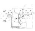
例えば、自動車等に搭載されている回転体の回転速度や回転方向を検出するために、回転検出装置が用いられている。図29に、従来から知られているこの種の回転検出装置2の構成を例示する。回転検出装置2は、回転体に対向して配置されている回転検出センサ520と、その回転検出センサ520から出力されるアナログ検出信号Va,Vbを処理する検出信号処理回路510を備えている。 For example, a rotation detection device is used to detect the rotation speed and rotation direction of a rotating body mounted on an automobile or the like. FIG. 29 illustrates a configuration of this type of
回転検出センサ520は、2個の磁気センサ520a,520bで構成されていることが多い。第1磁気センサ520aと第2磁気センサ520bは、回転体の外周面に対向して配置されている。回転体は磁性体で形成されており、その外周面には歯車状に歯山部と歯谷部が交互に形成されている。第1磁気センサ520aと第2磁気センサ520bは、回転体の周方向に沿って所定距離を隔てて配置されている。このため、回転体が回転すると、第1磁気センサ520aが出力する第1アナログ検出信号Vaと第2磁気センサ520bが出力する第2アナログ検出信号Vbは、例えば90°の位相差を有して推移する。検出信号処理回路510は、第1磁気センサ520aが出力する第1アナログ検出信号Vaと第2磁気センサ520bが出力する第2アナログ検出信号Vbを入力し、回転体の回転速度や回転方向が反映した出力信号Voutを出力する。 The
第1磁気センサ520aが出力する第1アナログ検出信号Vaは、検出信号処理回路510の第1変換回路530aに入力する。第1変換回路530aは、第1アナログ検出信号Vaを第1二値化検出信号Saに変換する。その第1二値化検出信号Saは、回転方向判定回路540に入力する。第2磁気センサ520bが出力する第2アナログ検出信号Vbは、検出信号処理回路510の第2変換回路530bに入力する。第2変換回路530bは、第2アナログ検出信号Vbを第2二値化検出信号Sbに変換する。その第2二値化検出信号Sbは、回転方向判定回路540に入力する。回転方向判定回路540は、第1二値化検出信号Saのレベルと第2二値化検出信号Sbのレベルの推移に基づいて回転体の回転方向を判定する。 The first analog detection signal Va output from the first
図30に、検出信号処理回路510のタイミングチャートを示す。例えば、回転方向判定回路540は、第2二値化検出信号Sbの立ち上がりのタイミングにおける第1二値化検出信号Saのレベルから回転体の回転方向を判定する。回転方向判定回路540は、第2二値化検出信号Sbの立ち上がりのタイミングにおいて第1二値化検出信号Saがハイレベルのときに、回転体が正回転していると判定する。回転方向判定回路540は、回転体が正回転していると判定すると、第1二値化検出信号Saを上側配線540Uに出力する(正回転信号Sa1)。一方、回転方向判定回路540は、第2二値化検出信号Sbの立ち上がりのタイミングにおいて第1二値化検出信号Saがローレベルのときに、回転体が逆回転していると判定する。回転方向判定回路540は、回転体が逆回転していると判定すると、第1二値化検出信号Saを下側配線540Dに出力する(逆回転信号Sa2)。 FIG. 30 shows a timing chart of the detection
上側配線540Uと下側配線540Dは、三値信号出力回路560に接続している。三値信号出力回路560は、上側配線540Uから正回転信号Sa1が入力すると、正回転信号Sa1に同期して全振幅で変動する出力信号Voutを出力する。三値信号出力回路560は、下側配線540Dから逆回転信号Sa2が入力すると、逆回転信号Sa2に同期して半振幅で変動する出力信号Voutを出力する。出力信号Voutは、その周波数が回転体の回転速度を反映しており、そのレベルの高さが回転方向を反映している。出力信号Voutは、回転体の回転速度と回転方向を反映した回転情報信号となる。 The
この種の回転体は、歯山部と歯谷部の間を往復するような振動を繰返すことがある。このような振動が発生すると、回転検出装置2は、回転体が正回転と逆回転を交互に繰返していることを示す出力信号Voutを生成する。 This type of rotating body may repeat vibrations that reciprocate between the tooth crest and the tooth root. When such vibration occurs, the
このような出力信号Voutが生成されるのを停止するために、特許文献1では、回路内にマスク回路を追加する技術を提案している。このマスク回路は、回転体が正回転と逆回転を交互に繰返すような振動に対し、一周期分の正回転信号Sa1及び逆回転信号Sa2をマスクすることによって、出力信号Voutが生成されるのを停止する。 In order to stop the generation of such an output signal Vout,
また、一般的に、回転体のギアの噛み合わせには遊びがある。このため、回転体が正回転と逆回転を交互に繰返すような振動以外に、内燃機関の振動等の影響によって回転体が微振動することがある。 In general, there is play in the meshing of the gears of the rotating body. For this reason, the rotating body may slightly vibrate due to the influence of the vibration of the internal combustion engine or the like, in addition to the vibration in which the rotating body repeats forward rotation and reverse rotation alternately.
変換回路の判定電圧に固定値が用いられていると、回転体の停止位置によっては、微振動による第1アナログ検出信号Vaと第2アナログ検出信号Vbのいずれか一方が二値化検出信号Sa,Sbに変換されてしまう場合がある。但し、このような場合でも、特許文献1で開示されるマスク回路が設けられていれば、出力信号Voutが生成されるのを停止することができる。この点においても、特許文献1で開示されるマスク回路は、極めて有用な技術であると言える。 When a fixed value is used for the determination voltage of the conversion circuit, depending on the stop position of the rotating body, one of the first analog detection signal Va and the second analog detection signal Vb due to slight vibration is the binarization detection signal Sa. , Sb may be converted. However, even in such a case, if the mask circuit disclosed in
しかしながら、例えば、変換回路に自動オフセット補正回路が用いられている場合、次のような問題が発生する。なお、自動オフセット補正回路とは、第1アナログ検出信号Vaと第2アナログ検出信号Vbのオフセット電圧が温度等によって変動するのを補償するために、第1アナログ検出信号Vaと第2アナログ検出信号Vbに追随して判定電圧を随時調整する回路のことをいう。変換回路に自動オフセット補正回路が用いられていると、微振動による第1アナログ検出信号Vaと第2アナログ検出信号Vbの双方が二値化検出信号Sa,Sbに変換されてしまう。微振動による第1アナログ検出信号Vaと第2アナログ検出信号Vbの位相差はほぼ0°又は180°であり、その周期が等しい正弦波である。このため、変換された二値化検出信号Sa,Sbは、回転体が正回転と逆回転を交互に繰返す場合の二値化検出信号Sa,Sb(位相差がほぼ0°又は180°であり、第1二値化検出信号Saと第2二値化検出信号Sbのデューティー比が異なる)とは異なる。変換された二値化検出信号Sa,Sbは、第1二値化検出信号Saと第2二値化検出信号Sbのデューティー比が等しく、位相差がほぼ0°又は180°となる。 However, for example, when an automatic offset correction circuit is used in the conversion circuit, the following problem occurs. The automatic offset correction circuit refers to the first analog detection signal Va and the second analog detection signal in order to compensate for fluctuations in the offset voltage of the first analog detection signal Va and the second analog detection signal Vb due to temperature or the like. A circuit that adjusts the determination voltage at any time following Vb. When the automatic offset correction circuit is used for the conversion circuit, both the first analog detection signal Va and the second analog detection signal Vb due to slight vibration are converted into the binary detection signals Sa and Sb. The phase difference between the first analog detection signal Va and the second analog detection signal Vb due to slight vibration is approximately 0 ° or 180 °, and is a sine wave having the same period. Therefore, the converted binarization detection signals Sa and Sb are binarization detection signals Sa and Sb (the phase difference is approximately 0 ° or 180 ° when the rotating body repeats forward rotation and reverse rotation alternately). The first binarization detection signal Sa and the second binarization detection signal Sb have different duty ratios). The converted binarization detection signals Sa and Sb have the same duty ratio between the first binarization detection signal Sa and the second binarization detection signal Sb, and the phase difference is substantially 0 ° or 180 °.
変換回路に自動オフセット補正回路が用いられている場合、微振動に対して発生されるデューティー比が等しい二値化検出信号Sa,Sbに対しては、第1アナログ検出信号Va又は第2アナログ検出信号Vbに含まれるノイズ等による影響で生じる二値化時の僅かな位相差検出誤差によって、特許文献1で開示されるマスク回路を用いたとしても、振動信号を出力信号Voutとして出力するという問題が発生する。また、変換回路に用いられているヒステリシスコンパレータ回路のヒステリシス電圧により生じる位相差検出誤差によっても、同様な問題が生じ得る。 When the automatic offset correction circuit is used for the conversion circuit, the first analog detection signal Va or the second analog detection is used for the binarization detection signals Sa and Sb having the same duty ratio generated with respect to the minute vibration. Even if the mask circuit disclosed in
本発明は、回転体の回転速度や回転方向を検出する検出信号処理回路において、回転体の振動による出力信号の誤生成を抑制する技術を提供することを目的としている。さらに、本発明は、そのような検出信号処理回路を備えた回転検出装置を提供することを目的としている。 An object of the present invention is to provide a technique for suppressing erroneous generation of an output signal due to vibration of a rotating body in a detection signal processing circuit that detects the rotational speed and direction of the rotating body. Furthermore, an object of the present invention is to provide a rotation detection device provided with such a detection signal processing circuit.
本明細書で開示される技術は、回転検出センサから出力される第1アナログ検出信号と第2アナログ検出信号の位相差に基づいて、振動による出力信号の誤生成を抑制することを特徴としている。回転体に対向して配置されている回転検出センサは、回転体の周方向に沿って所定距離を隔てて配置されており、回転検出センサが出力する第1アナログ検出信号と第2アナログ検出信号は、回転体が正回転又は逆回転をしていれば、例えば60〜90°の位相差を有して推移する。 The technology disclosed in this specification is characterized by suppressing erroneous generation of an output signal due to vibration based on the phase difference between the first analog detection signal and the second analog detection signal output from the rotation detection sensor. . The rotation detection sensor disposed facing the rotating body is disposed at a predetermined distance along the circumferential direction of the rotating body, and the first analog detection signal and the second analog detection signal output from the rotation detection sensor. If the rotating body is rotating forward or backward, the phase shifts with a phase difference of 60 to 90 °, for example.
一方、微振動に基づいて出力される第1アナログ検出信号と第2アナログ検出信号は、停止位置に基づいてほぼ0°又は180°の位相差を有して推移する。図31は、回転体が正回転しているときに、第1磁気センサ及び第2磁気センサから90°の位相差を有して出力される第1アナログ検出信号Vaと第2アナログ検出信号Vbの波形を示している。例えば、回転体が停止位置SP1で停止したとする。このとき、回転体に上記微振動が生じると、第1磁気センサと第2磁気センサは、位相差がほぼ0°の第1アナログ検出信号Vaと第2アナログ検出信号Vbを出力する。例えば、回転体が停止位置SP2で停止したとする。このとき、回転体に上記微振動が生じると、第1磁気センサと第2磁気センサは、位相差がほぼ180°の第1アナログ検出信号Vaと第2アナログ検出信号Vbを出力する。即ち、回転体が正回転又は逆回転しているときの第1アナログ検出信号と第2アナログ検出信号の位相差と、回転体が微振動しているときの第1アナログ検出信号と第2アナログ検出信号の位相差の間には明白な差異があり、この位相差の差異に基づいて両者を区別することが可能である。本明細書で開示される技術は、この位相差の差異に基づいて振動による出力信号の誤生成を抑制することを特徴としている。 On the other hand, the first analog detection signal and the second analog detection signal output based on the slight vibration change with a phase difference of approximately 0 ° or 180 ° based on the stop position. FIG. 31 shows a first analog detection signal Va and a second analog detection signal Vb output with a phase difference of 90 ° from the first magnetic sensor and the second magnetic sensor when the rotating body is rotating forward. The waveform is shown. For example, assume that the rotating body stops at the stop position SP1. At this time, when the fine vibration occurs in the rotating body, the first magnetic sensor and the second magnetic sensor output the first analog detection signal Va and the second analog detection signal Vb having a phase difference of approximately 0 °. For example, assume that the rotating body stops at the stop position SP2. At this time, when the fine vibration occurs in the rotating body, the first magnetic sensor and the second magnetic sensor output the first analog detection signal Va and the second analog detection signal Vb having a phase difference of approximately 180 °. That is, the phase difference between the first analog detection signal and the second analog detection signal when the rotating body is rotating forward or backward, and the first analog detection signal and the second analog when the rotating body is slightly vibrating. There is a clear difference between the phase differences of the detection signals, and it is possible to distinguish between them based on this phase difference difference. The technique disclosed in this specification is characterized by suppressing erroneous generation of an output signal due to vibration based on the difference in phase difference.
本明細書で開示される検出信号処理回路は、回転体が回転しているときに、回転体に対向して配置された回転検出センサから位相差を有して出力される第1アナログ検出信号と第2アナログ検出信号を処理する。検出信号処理回路は、第1変換回路と第2変換回路と回転方向判定回路とマスク回路と位相差判定回路とを備えている。第1変換回路は、第1アナログ検出信号を第1二値化検出信号に変換する。第2変換回路は、第2アナログ検出信号を第2二値化検出信号に変換する。回転方向判定回路は、第1二値化検出信号のレベルと第2二値化検出信号のレベルの推移に基づいて回転体の回転方向を判定し、回転体の回転速度と回転方向の情報を含む回転情報信号を出力する。マスク回路は、回転方向判定回路の出力線に接続されており、回転情報信号に含まれる情報の伝達の停止を実行可能に構成されている。位相差判定回路は、第1アナログ検出信号と第2アナログ検出信号の位相差が所定範囲外のときに、回転情報信号の変動の停止を要求する位相差停止要求信号を出力する。
ここで、第1二値化検出信号と第2二値化検出信号は、回転体が正回転しているときに、第1二値化検出信号と第2二値化検出信号がこの順で変動するとしてもよく、あるいは第2二値化検出信号と第1二値化検出信号がこの順で変動するとしてもよい。即ち、回転体が正回転しているときに、第1二値化検出信号がローからハイに変動した後に、第2二値化検出信号がローからハイに変動してもよい。あるいは、回転体が正回転しているときに、第2二値化検出信号がローからハイに変動した後に、第1二値化検出信号がローからハイに変動してもよい。
「第1アナログ検出信号と第2アナログ検出信号の位相差」には、「第1アナログ検出信号に応じて変動する信号と第2アナログ検出信号に応じて変動する信号の位相差」が含まれる。「第1アナログ検出信号に応じて変動する信号」とは、第1アナログ検出信号に同期(多少の時間ズレは許容される)して変動する信号であり、例えば、第1アナログ検出信号を増幅した信号、第1変換回路で変換された第1二値化検出信号が含まれる。「第2アナログ検出信号に応じて変動する信号」も同様である。
また、「回転情報信号」とは、回転方向判定回路から直接的に出力される信号の他に、回転方向判定回路から出力された後に処理された信号も含む。例えば、回転情報信号の一例には、回転方向判定回路から出力された後に三値信号出力回路によって処理された三値信号も含まれる。
また、「位相差停止要求信号」は、これを要件としてマスク回路において回転情報信号に含まれる情報の伝達を停止するものに限られない。複数の「位相差停止要求信号」を考慮して、回転情報信号に含まれる情報の伝達を停止させてもよい。また、他の判定回路からの「停止要求信号」を考慮して回転情報信号の変動を停止させてもよい。The detection signal processing circuit disclosed in the present specification is a first analog detection signal that is output with a phase difference from a rotation detection sensor disposed to face the rotating body when the rotating body is rotating. And processing the second analog detection signal. The detection signal processing circuit includes a first conversion circuit, a second conversion circuit, a rotation direction determination circuit, a mask circuit, and a phase difference determination circuit. The first conversion circuit converts the first analog detection signal into a first binarization detection signal. The second conversion circuit converts the second analog detection signal into a second binarization detection signal. The rotation direction determination circuit determines the rotation direction of the rotating body based on the transition of the level of the first binarization detection signal and the level of the second binarization detection signal, and obtains information on the rotation speed and rotation direction of the rotation body. Output rotation information signal including. The mask circuit is connected to the output line of the rotation direction determination circuit, and is configured to be able to stop transmission of information included in the rotation information signal. The phase difference determination circuit outputs a phase difference stop request signal for requesting to stop the fluctuation of the rotation information signal when the phase difference between the first analog detection signal and the second analog detection signal is outside a predetermined range.
Here, the first binarization detection signal and the second binarization detection signal are the first binarization detection signal and the second binarization detection signal in this order when the rotating body is rotating forward. The second binarization detection signal and the first binarization detection signal may fluctuate in this order. That is, when the rotating body is rotating forward, the second binarization detection signal may change from low to high after the first binarization detection signal changes from low to high. Alternatively, the first binarization detection signal may fluctuate from low to high after the second binarization detection signal fluctuates from low to high when the rotating body is rotating forward.
The “phase difference between the first analog detection signal and the second analog detection signal” includes “the phase difference between the signal that varies according to the first analog detection signal and the signal that varies according to the second analog detection signal”. . The “signal that fluctuates according to the first analog detection signal” is a signal that fluctuates in synchronization with the first analog detection signal (a slight time shift is allowed). For example, the first analog detection signal is amplified. And the first binarization detection signal converted by the first conversion circuit. The same applies to the “signal that varies according to the second analog detection signal”.
The “rotation information signal” includes not only a signal directly output from the rotation direction determination circuit but also a signal processed after being output from the rotation direction determination circuit. For example, an example of the rotation information signal includes a ternary signal that is output from the rotation direction determination circuit and then processed by the ternary signal output circuit.
In addition, the “phase difference stop request signal” is not limited to a signal that stops transmission of information included in the rotation information signal in the mask circuit with this as a requirement. In consideration of a plurality of “phase difference stop request signals”, transmission of information included in the rotation information signal may be stopped. Further, the fluctuation of the rotation information signal may be stopped in consideration of a “stop request signal” from another determination circuit.
位相差判定回路は、デジタル位相差判定回路を備えていることが好ましい。そのデジタル位相差判定回路は、第1二値化検出信号を遅延させた遅延第1二値化検出信号を生成する回路と、第1二値化検出信号のレベルが切換わるタイミングと第2二値化検出信号のレベルが切換わるタイミングの間に、遅延第1二値化検出信号のレベルが切換わるタイミングが存在するか否かを判定する回路とを備えているのが好ましい。このデジタル位相差判定回路は、遅延第1二値化検出信号のレベルが切換わるタイミングが第1二値化検出信号のレベルが切換わるタイミングと第2二値化検出信号のレベルが切換わるタイミングの間に存在しないときに、回転情報信号に含まれる情報の伝達の停止を要求する位相差停止要求信号を出力する。
例えば、回転体が正回転しているときに、第1二値化検出信号と第2二値化検出信号がこの順で変動し、90°の位相差を有して推移すると仮定する。即ち、回転体が正回転しているときに、第1二値化検出信号がローからハイに変動した後に、90°の位相差を有して第2二値化検出信号がローからハイに変動すると仮定する。この場合、遅延第1二値化検出信号を第1二値化検出信号に対して30°の位相差を有するように生成したとすると、回転体が正回転していれば、第1二値化検出信号のレベルが切換わるタイミングと第2二値化検出信号のレベルが切換わるタイミングの間に、遅延第1二値化検出信号のレベルが切換わるタイミングが存在するはずである。一方、回転体が微振動する場合は、第1二値化検出信号と第2二値化検出信号の位相差がほぼ0°(なお、位相差が180°の場合は、後述する反転信号を利用すればよい)であり、第1二値化検出信号のレベルが切換わるタイミングと第2二値化検出信号のレベルが切換わるタイミングの間に、遅延第1二値化検出信号のレベルが切換わるタイミングが存在しない。このように、遅延第1二値化検出信号を利用する技術は、回転体が正回転しているときの第1二値化検出信号と第2二値化検出信号の位相差と、回転体が微振動しているときの第1二値化検出信号と第2二値化検出信号の位相差の差異を判定するのに有用なものである。なお、回転体が正回転している場合と逆回転している場合の双方を同時に考慮するならば、デジタル位相差判定回路は、第2二値化検出信号を遅延させた遅延第2二値化検出信号を生成する回路と、第1二値化検出信号のレベルが切換わるタイミングと第2二値化検出信号のレベルが切換わるタイミングの間に、遅延第2二値化検出信号のレベルが切換わるタイミングが存在するか否かを判定する回路とをさらに備えているのが好ましい。このデジタル位相差判定回路は、遅延第2二値化検出信号のレベルが切換わるタイミングが第1二値化検出信号のレベルが切換わるタイミングと第2二値化検出信号のレベルが切換わるタイミングの間に存在しないときに、回転情報信号に含まれる情報の伝達の停止を要求する位相差停止要求信号を出力する。The phase difference determination circuit preferably includes a digital phase difference determination circuit. The digital phase difference determination circuit includes a circuit that generates a delayed first binarization detection signal obtained by delaying the first binarization detection signal, a timing at which the level of the first binarization detection signal is switched, and a second second It is preferable to include a circuit for determining whether or not there is a timing at which the level of the delayed first binarization detection signal is switched between timings at which the level of the binarization detection signal is switched. In this digital phase difference determination circuit, the timing at which the level of the delayed first binarization detection signal is switched is the timing at which the level of the first binarization detection signal is switched and the timing at which the level of the second binarization detection signal is switched. When the signal does not exist, a phase difference stop request signal for requesting stop of transmission of information included in the rotation information signal is output.
For example, it is assumed that when the rotating body is rotating forward, the first binarization detection signal and the second binarization detection signal fluctuate in this order and change with a phase difference of 90 °. That is, when the rotating body is rotating forward, after the first binarization detection signal changes from low to high, the second binarization detection signal changes from low to high with a phase difference of 90 °. Assume that it fluctuates. In this case, assuming that the delayed first binarization detection signal is generated so as to have a phase difference of 30 ° with respect to the first binarization detection signal, if the rotating body is rotating forward, the first binary There should be a timing for switching the level of the delayed first binarization detection signal between the timing for switching the level of the binarization detection signal and the timing for switching the level of the second binarization detection signal. On the other hand, when the rotating body vibrates slightly, the phase difference between the first binarization detection signal and the second binarization detection signal is approximately 0 ° (in the case where the phase difference is 180 °, an inverted signal described later is used). The level of the delayed first binarization detection signal is between the timing when the level of the first binarization detection signal is switched and the timing when the level of the second binarization detection signal is switched. There is no timing to switch. Thus, the technique using the delayed first binarization detection signal is based on the phase difference between the first binarization detection signal and the second binarization detection signal when the rotator is rotating forward, and the rotator. This is useful for determining the difference in phase difference between the first binarization detection signal and the second binarization detection signal when is slightly vibrating. If both the case where the rotating body is rotating forward and the case where it is rotating backward are considered at the same time, the digital phase difference determination circuit delays the second binarization detection signal. The level of the delayed second binarization detection signal between the circuit for generating the binarization detection signal, the timing at which the level of the first binarization detection signal is switched, and the timing at which the level of the second binarization detection signal is switched It is preferable to further include a circuit for determining whether or not there is a timing for switching between. In this digital phase difference determination circuit, the timing at which the level of the delayed second binarization detection signal is switched is the timing at which the level of the first binarization detection signal is switched and the timing at which the level of the second binarization detection signal is switched. When the signal does not exist, a phase difference stop request signal for requesting stop of transmission of information included in the rotation information signal is output.
デジタル位相差判定回路は、反転した反転第2二値化検出信号を遅延させた反転遅延第2二値化検出信号を生成する遅延二値化検出信号生成回路と、第1二値化検出信号のレベルが切換わるタイミングと反転第2二値化検出信号のレベルが切換わるタイミングの間に、反転遅延第2二値化検出信号のレベルが切換わるタイミングが存在するか否かを判定する回路とをさらに備えているのが好ましい。このデジタル位相差判定回路は、反転遅延第2二値化検出信号のレベルが切換わるタイミングが第1二値化検出信号のレベルが切換わるタイミングと反転第2二値化検出信号のレベルが切換わるタイミングの間に存在しないときに、回転情報信号に含まれる情報の伝達の停止を要求する位相差停止要求信号を出力する。
微振動による第1二値化検出信号と第2二値化検出信号の位相差は、停止位置によって180°の場合もある。デジタル位相差判定回路が反転信号を利用するように構成されていると、このような微振動をも判定することができる。The digital phase difference determination circuit includes a delayed binarization detection signal generation circuit that generates an inverted delayed second binarization detection signal obtained by delaying an inverted inverted second binarization detection signal, and a first binarization detection signal Circuit for determining whether or not there is a timing for switching the level of the inverted delayed second binarization detection signal between the timing for switching the level of the second and the level of the inverted second binarization detection signal Are preferably further provided. In this digital phase difference determination circuit, the timing at which the level of the inverted binary binarization detection signal is switched is switched between the timing at which the level of the first binarization detection signal is switched and the level of the inverted second binarization detection signal. When it does not exist during the switching timing, a phase difference stop request signal for requesting stop of transmission of information included in the rotation information signal is output.
The phase difference between the first binarization detection signal and the second binarization detection signal due to slight vibration may be 180 ° depending on the stop position. If the digital phase difference determination circuit is configured to use an inverted signal, it is also possible to determine such a slight vibration.
遅延二値化検出信号生成回路は、第1アナログ検出信号の正のピーク電圧と第1アナログ検出信号の負のピーク電圧の間に設定されている電圧を基準閾値とし、その基準閾値と前記正のピーク電圧の間に設定されている電圧を高側オフセット閾値とし、その基準閾値の前記負のピーク電圧の間に設定されている電圧を低側オフセット閾値としたときに、第1アナログ検出信号が高側オフセット閾値を上回った時と第1アナログ検出信号が低側オフセット閾値を下回った時に、出力をハイとローの間で反転させることが好ましい。
高側オフセット閾値と低側オフセット閾値を利用することで、極めて簡易に遅延二値化検出信号を生成することができる。The delay binarization detection signal generation circuit uses a voltage set between the positive peak voltage of the first analog detection signal and the negative peak voltage of the first analog detection signal as a reference threshold, and the reference threshold and the positive The first analog detection signal when the voltage set between the peak voltages of the first and second negative voltages is the high-side offset threshold and the voltage set between the negative peak voltages of the reference threshold is the low-side offset threshold. Preferably, the output is inverted between high and low when is above the high offset threshold and when the first analog detection signal is below the low offset threshold.
By using the high-side offset threshold and the low-side offset threshold, it is possible to generate the delayed binarization detection signal very easily.
上記の遅延二値化検出信号生成回路は、例えば、遅延二値化検出信号生成回路用の第1比較回路と第2比較回路と選択回路によって構築することができる。遅延二値化検出信号生成回路用の第1比較回路は、第1アナログ検出信号が基準閾値を下回った時に出力を反転させるとともに閾値を高側オフセット閾値に切換え、第1アナログ検出信号が高側オフセット閾値を上回った時に出力を反転させるとともに閾値を基準閾値に切換える。遅延二値化検出信号生成回路用の第2比較回路は、第1アナログ検出信号が基準閾値を上回った時に出力を反転させるとともに閾値を低側オフセット閾値に切換え、第1アナログ検出信号が低側オフセット閾値を下回った時に出力を反転させるとともに閾値を基準閾値に切換える。遅延二値化検出信号生成回路用の選択回路は、第1比較回路と第2比較回路の出力を入力しており、第1アナログ検出信号が高側オフセット閾値を上回った時に生じる第1比較回路の出力反転現象と、第1アナログ検出信号が低側オフセット閾値を下回った時に生じる第2比較回路の出力反転現象を選択し、出力をハイとローの間で反転させる。 The delay binarization detection signal generation circuit can be constructed by, for example, a first comparison circuit, a second comparison circuit, and a selection circuit for the delay binarization detection signal generation circuit. The first comparison circuit for the delay binarization detection signal generation circuit inverts the output when the first analog detection signal falls below the reference threshold and switches the threshold to the high-side offset threshold so that the first analog detection signal is on the high side. When the offset threshold is exceeded, the output is inverted and the threshold is switched to the reference threshold. The second comparison circuit for the delay binarization detection signal generation circuit inverts the output when the first analog detection signal exceeds the reference threshold and switches the threshold to the low-side offset threshold so that the first analog detection signal is low When the value falls below the offset threshold, the output is inverted and the threshold is switched to the reference threshold. The selection circuit for the delayed binarization detection signal generation circuit receives the outputs of the first comparison circuit and the second comparison circuit, and the first comparison circuit is generated when the first analog detection signal exceeds the high-side offset threshold value. And the output inversion phenomenon of the second comparison circuit that occurs when the first analog detection signal falls below the low-side offset threshold, and the output is inverted between high and low.
本明細書で開示される検出信号処理回路では、第1変換回路は、第1アナログ検出信号の正のピーク電圧を検出する第1正ピーク電圧ホールド回路と、第1アナログ検出信号の負のピーク電圧を検出する第1負ピーク電圧ホールド回路と、第1オフセット回路とを備えているのが好ましい。第1変換回路は、正のピーク電圧と負のピーク電圧の間に設定されている電圧を利用して第1アナログ検出信号を第1二値化検出信号に変換する。第1オフセット回路は、第1正ピーク電圧ホールド回路が維持している正のピーク電圧を経時的に減少させるとともに、第1負ピーク電圧ホールド回路が維持している負のピーク電圧を経時的に上昇させている。さらに、第2変換回路は、第2アナログ検出信号の正のピーク電圧を検出する第2正ピーク電圧ホールド回路と、第2アナログ検出信号の負のピーク電圧を検出する第2負ピーク電圧ホールド回路と、第2オフセット回路とを備えているのが好ましい。第2変換回路は、正のピーク電圧と負のピーク電圧の間に設定されている電圧を利用して第2アナログ検出信号を第2二値化検出信号に変換する。第2オフセット回路は、第2正ピーク電圧ホールド回路が維持している正のピーク電圧を経時的に減少させるとともに、第2負ピーク電圧ホールド回路が維持している負のピーク電圧を経時的に上昇させている。
前記したように、オフセット回路を有する比較回路を用いると、振幅の小さいアナログ検出信号も二値化検出信号に変換するので、微振動に基づく出力信号の誤生成が発生する。したがって、オフセット回路を有する比較回路と位相差判定回路を組み合わせることは、オフセット回路に特有の課題を解決するという点で有用である。ただし、本明細書で開示される技術は、比較回路がオフセット回路を有していない場合でも有用である。本明細書で開示される技術は、回転体が正回転又は逆回転しているときの第1アナログ検出信号と第2アナログ検出信号の位相差と、回転体が微振動しているときの第1アナログ検出信号と第2アナログ検出信号の位相差の差異に着目し、その差異を利用して回転体の回転に基づく信号変化と回転体の微振動に基づく信号変化を判定することを特徴としている。この技術に係る位相差判定回路は、オフセット回路を有する比較回路と組み合わせなくても、有用な結果を提供するものである。In the detection signal processing circuit disclosed in this specification, the first conversion circuit includes a first positive peak voltage hold circuit that detects a positive peak voltage of the first analog detection signal, and a negative peak of the first analog detection signal. It is preferable that a first negative peak voltage hold circuit for detecting a voltage and a first offset circuit are provided. The first conversion circuit converts the first analog detection signal into the first binarization detection signal using a voltage set between the positive peak voltage and the negative peak voltage. The first offset circuit decreases the positive peak voltage maintained by the first positive peak voltage hold circuit with time and reduces the negative peak voltage maintained by the first negative peak voltage hold circuit with time. It is rising. Further, the second conversion circuit includes a second positive peak voltage hold circuit that detects a positive peak voltage of the second analog detection signal, and a second negative peak voltage hold circuit that detects a negative peak voltage of the second analog detection signal. And a second offset circuit. The second conversion circuit converts the second analog detection signal into the second binarization detection signal using a voltage set between the positive peak voltage and the negative peak voltage. The second offset circuit decreases the positive peak voltage maintained by the second positive peak voltage hold circuit with time and reduces the negative peak voltage maintained by the second negative peak voltage hold circuit with time. It is rising.
As described above, when a comparison circuit having an offset circuit is used, an analog detection signal having a small amplitude is also converted into a binarization detection signal, so that an output signal is erroneously generated based on slight vibration. Therefore, combining a comparison circuit having an offset circuit and a phase difference determination circuit is useful in that it solves problems peculiar to the offset circuit. However, the technique disclosed in this specification is useful even when the comparison circuit does not have an offset circuit. The technology disclosed in this specification is based on the phase difference between the first analog detection signal and the second analog detection signal when the rotating body is rotating forward or backward, and the first difference when the rotating body is slightly vibrating. Focusing on the difference in phase difference between the first analog detection signal and the second analog detection signal, and using the difference, signal change based on rotation of the rotating body and signal change based on slight vibration of the rotating body are determined. Yes. The phase difference determination circuit according to this technique provides a useful result without being combined with a comparison circuit having an offset circuit.
本明細書で開示される検出信号処理回路では、第1変換回路は、正のピーク電圧と負のピーク電圧の間に設定されている電圧を第1基準閾値とし、その第1基準閾値と前記正のピーク電圧の間に設定されている電圧を高側オフセット閾値とし、その第1基準閾値の前記負のピーク電圧の間に設定されている電圧を低側オフセット閾値としたときに、高側オフセット閾値と低側オフセット閾値の間で比較閾値を切換えて第1アナログ検出信号を第1二値化検出信号に変換する第1ヒステリシスコンパレータ回路を有しているのが好ましい。さらに、第2変換回路も、正のピーク電圧と負のピーク電圧の間に設定されている電圧を第2基準閾値とし、その第2基準閾値と前記正のピーク電圧の間に設定されている電圧を高側オフセット閾値とし、その第2基準閾値の前記負のピーク電圧の間に設定されている電圧を低側オフセット閾値としたときに、高側オフセット閾値と低側オフセット閾値の間で比較閾値を切換えて第2アナログ検出信号を第2二値化検出信号に変換する第2ヒステリシスコンパレータ回路を有していることが好ましい。 In the detection signal processing circuit disclosed in this specification, the first conversion circuit uses a voltage set between a positive peak voltage and a negative peak voltage as a first reference threshold, and the first reference threshold and the When the voltage set between the positive peak voltages is the high side offset threshold and the voltage set between the negative peak voltages of the first reference threshold is the low side offset threshold, the high side It is preferable to have a first hysteresis comparator circuit that switches the comparison threshold value between the offset threshold value and the low-side offset threshold value to convert the first analog detection signal into the first binarization detection signal. Further, the second conversion circuit also sets the voltage set between the positive peak voltage and the negative peak voltage as the second reference threshold, and is set between the second reference threshold and the positive peak voltage. When the voltage is set as the high-side offset threshold and the voltage set between the negative peak voltages of the second reference threshold is set as the low-side offset threshold, the comparison is made between the high-side offset threshold and the low-side offset threshold. It is preferable to have a second hysteresis comparator circuit that switches the threshold and converts the second analog detection signal into a second binarization detection signal.
第1変換回路の第1ヒステリシスコンパレータ回路は、第1変換回路用の第1比較回路と第2比較回路と選択回路を有しているのが好ましい。この場合、第1変換回路用の第1比較回路は、第1アナログ検出信号が第1基準閾値を下回った時に出力を反転させるとともに比較閾値を高側オフセット閾値に切換え、第1アナログ検出信号が高側オフセット閾値を上回った時に出力を反転させるとともに比較閾値を第1基準閾値に切換える。第1変換回路用の第2比較回路は、第1アナログ検出信号が第1基準閾値を上回った時に出力を反転させるとともに比較閾値を低側オフセット閾値に切換え、第1アナログ検出信号が低側オフセット閾値を下回った時に出力を反転させるとともに比較閾値を第1基準閾値に切換える。第1変換回路用の選択回路は、第1アナログ検出信号が第1基準閾値を下回った時に生じる出力反転現象と、第1アナログ検出信号が第1基準閾値を上回った時に生じる出力反転現象を選択して出力をハイとローの間で反転させて出力する。
また、第2変換回路の第2ヒステリシスコンパレータ回路は、第2変換回路用の第1比較回路と第2比較回路と選択回路を有しているのが好ましい。この場合、第2変換回路用の第1比較回路路は、第2アナログ検出信号が第2基準閾値を下回った時に出力を反転させるとともに比較閾値を高側オフセット閾値に切換え、第2アナログ検出信号が高側オフセット閾値を上回った時に出力を反転させるとともに比較閾値を第2基準閾値に切換える。第2変換回路用の第2比較回路は、第2アナログ検出信号が第2基準閾値を上回った時に出力を反転させるとともに比較閾値を低側オフセット閾値に切換え、第2アナログ検出信号が低側オフセット閾値を下回った時に出力を反転させるとともに比較閾値を第2基準閾値に切換える。第2変換回路用の選択回路は、第2アナログ検出信号が第2基準閾値を下回った時に生じる出力反転現象と、第2アナログ検出信号が第2基準閾値を上回った時に生じる出力反転現象を選択して出力をハイとローの間で反転させて出力する。
従来のヒステリシスコンパレータ回路は、比較閾値に高側オフセット閾値と低側オフセット閾値を利用しており、正確な二値化検出信号よりも時間遅れが生じていた。上記のヒステリシスコンパレータ回路では、基準閾値を下回った時及び上回った時に反転する二値化検出信号を生成するので、高精度なものとなる。
なお、上記の検出信号処理回路では、第1変換回路用の第1比較回路と遅延二値化検出信号生成回路用の第1比較回路に共通のものを用い、第1変換回路用の第2比較回路と遅延二値化検出信号生成回路用の第2比較回路に共通のものを用い、第2変換回路用の第1比較回路と遅延二値化検出信号生成回路用の第1比較回路に共通のものを用い、第2変換回路用の第2比較回路と遅延二値化検出信号生成回路用の第2比較回路に共通のものを用いるのが好ましい。The first hysteresis comparator circuit of the first conversion circuit preferably includes a first comparison circuit for the first conversion circuit, a second comparison circuit, and a selection circuit. In this case, the first comparison circuit for the first conversion circuit inverts the output when the first analog detection signal falls below the first reference threshold and switches the comparison threshold to the high-side offset threshold. When the high-side offset threshold is exceeded, the output is inverted and the comparison threshold is switched to the first reference threshold. The second comparison circuit for the first conversion circuit inverts the output when the first analog detection signal exceeds the first reference threshold and switches the comparison threshold to the low-side offset threshold, so that the first analog detection signal is low-side offset. When the value falls below the threshold, the output is inverted and the comparison threshold is switched to the first reference threshold. The selection circuit for the first conversion circuit selects an output inversion phenomenon that occurs when the first analog detection signal falls below the first reference threshold, and an output inversion phenomenon that occurs when the first analog detection signal exceeds the first reference threshold. The output is inverted between high and low and output.
The second hysteresis comparator circuit of the second conversion circuit preferably includes a first comparison circuit, a second comparison circuit, and a selection circuit for the second conversion circuit. In this case, the first comparison circuit path for the second conversion circuit inverts the output when the second analog detection signal falls below the second reference threshold value and switches the comparison threshold value to the high-side offset threshold value. When the value exceeds the high-side offset threshold, the output is inverted and the comparison threshold is switched to the second reference threshold. The second comparison circuit for the second conversion circuit inverts the output when the second analog detection signal exceeds the second reference threshold and switches the comparison threshold to the low-side offset threshold, so that the second analog detection signal is low-side offset. When the value falls below the threshold, the output is inverted and the comparison threshold is switched to the second reference threshold. The selection circuit for the second conversion circuit selects an output inversion phenomenon that occurs when the second analog detection signal falls below the second reference threshold value, and an output inversion phenomenon that occurs when the second analog detection signal exceeds the second reference threshold value. The output is inverted between high and low and output.
A conventional hysteresis comparator circuit uses a high-side offset threshold and a low-side offset threshold as comparison thresholds, and a time delay occurs compared to an accurate binarization detection signal. The above hysteresis comparator circuit generates a binarization detection signal that is inverted when the reference threshold value is below and above the reference threshold value.
In the above detection signal processing circuit, a common circuit is used for the first comparison circuit for the first conversion circuit and the first comparison circuit for the delay binarization detection signal generation circuit, and the second conversion circuit for the first conversion circuit is used. A common comparison circuit and a second comparison circuit for the delay binarization detection signal generation circuit are used, and the first comparison circuit for the second conversion circuit and the first comparison circuit for the delay binarization detection signal generation circuit are used. It is preferable to use a common one for the second comparison circuit for the second conversion circuit and a second comparison circuit for the delayed binarization detection signal generation circuit.
本明細書で開示される検出信号処理回路は、少なくとも第1アナログ検出信号又は第2アナログ検出信号のいずれか一方の振幅が所定値よりも小さいときに、回転情報信号に含まれる情報の伝達の停止を要求する振幅停止要求信号を出力する振幅判定回路をさらに備えていることが好ましい。なお、検出信号処理回路は、第1アナログ検出信号及び第2アナログ検出信号の双方の振幅が所定値よりも小さいときに、振幅停止要求信号を出力する振幅判定回路を備えていてもよい。
ここで、「振幅停止要求信号」は、これを要件としてマスク回路において回転情報信号に含まれる情報の伝達を停止するものに限られない。複数の「振幅停止要求信号」を考慮して、回転情報信号に含まれる情報の伝達を停止させてもよい。また、他の判定回路からの「停止要求信号」を考慮して回転情報信号の変動を停止させてもよい。
回転体が微振動したときに出力される第1アナログ検出信号又は第2アナログ検出信号の振幅は、回転体が正回転又は逆回転しているときに出力される第1アナログ検出信号又は第2アナログ検出信号の振幅よりも圧倒的に小さい。これは、回転体が微振動している場合、停止位置付近での微振動であり、位相角の変化が小さいからである。したがって、第1アナログ検出信号又は第2アナログ検出信号の振幅に基づいて、回転体が微振動していることを判定することができる。この判定結果に基づいて、出力信号の誤生成を抑制することができる。位相差判定回路と振幅判定回路を組み合わせると、出力信号の誤生成をさらに抑制することができる。The detection signal processing circuit disclosed in this specification is configured to transmit information included in the rotation information signal when the amplitude of at least one of the first analog detection signal and the second analog detection signal is smaller than a predetermined value. It is preferable to further include an amplitude determination circuit that outputs an amplitude stop request signal for requesting the stop. The detection signal processing circuit may include an amplitude determination circuit that outputs an amplitude stop request signal when the amplitudes of both the first analog detection signal and the second analog detection signal are smaller than a predetermined value.
Here, the “amplitude stop request signal” is not limited to a signal that stops transmission of information included in the rotation information signal in the mask circuit with this as a requirement. In consideration of a plurality of “amplitude stop request signals”, transmission of information included in the rotation information signal may be stopped. Further, the fluctuation of the rotation information signal may be stopped in consideration of a “stop request signal” from another determination circuit.
The amplitude of the first analog detection signal or the second analog detection signal that is output when the rotating body vibrates slightly is the first analog detection signal or the second analog detection signal that is output when the rotating body is rotating forward or reverse. It is overwhelmingly smaller than the amplitude of the analog detection signal. This is because when the rotating body vibrates slightly, it is slightly vibrated near the stop position and the change in the phase angle is small. Therefore, it can be determined that the rotating body is slightly vibrating based on the amplitude of the first analog detection signal or the second analog detection signal. Based on the determination result, erroneous generation of the output signal can be suppressed. Combining the phase difference determination circuit and the amplitude determination circuit can further suppress erroneous generation of the output signal.
本明細書で開示される検出信号処理回路は、回転体が正回転から逆回転、又は逆回転から正回転に反転した後の最初の回転情報信号に含まれる情報の伝達の停止を要求する反転停止要求信号を出力する反転判定回路をさらに備えていることが好ましい。
ここで、「反転停止要求信号」は、これを要件としてマスク回路において回転情報信号に含まれる情報の伝達を停止するものに限られない。複数の「反転停止要求信号」を考慮して、回転情報信号に含まれる情報の伝達を停止させてもよい。また、他の判定回路からの「停止要求信号」を考慮して回転情報信号の変動を停止させてもよい。
反転判定回路は、回転体が正回転と逆回転を交互に繰返すような振動の影響を抑制することができる。位相差判定回路と反転判定回路を組み合わせると、位相差判定回路が比較的に小さな振動の影響を抑制し、反転判定回路が比較的に大きな振動の影響を抑制する。位相差判定回路と反転判定回路を組み合わせると、様々な種類の振動の影響を抑制することが可能になる。The detection signal processing circuit disclosed in the present specification is a reversal requesting the stop of transmission of information included in the first rotation information signal after the rotating body is reversed from normal rotation to reverse rotation or reverse rotation to normal rotation. It is preferable to further include an inversion determination circuit that outputs a stop request signal.
Here, the “inversion stop request signal” is not limited to the signal that stops the transmission of information included in the rotation information signal in the mask circuit as a requirement. In consideration of a plurality of “inversion stop request signals”, the transmission of information included in the rotation information signal may be stopped. Further, the fluctuation of the rotation information signal may be stopped in consideration of a “stop request signal” from another determination circuit.
The inversion determination circuit can suppress the influence of vibration that causes the rotating body to repeat forward rotation and reverse rotation alternately. When the phase difference determination circuit and the inversion determination circuit are combined, the phase difference determination circuit suppresses the influence of relatively small vibration, and the inversion determination circuit suppresses the influence of relatively large vibration. Combining the phase difference determination circuit and the inversion determination circuit makes it possible to suppress the effects of various types of vibrations.
本明細書で開示される遅延二値化検出信号生成回路は、他の用途に利用してもよい。様々な局面で二値化信号から遅延二値化信号を生成したいことがあり、本明細書で開示される遅延二値化検出信号生成回路は、そのような局面で広く利用され得る。 The delayed binarization detection signal generation circuit disclosed in this specification may be used for other purposes. There are cases where it is desired to generate a delayed binarized signal from a binarized signal in various aspects, and the delayed binarized detection signal generation circuit disclosed in this specification can be widely used in such an aspect.
本発明の検出信号処理回路によると、回転体の振動による出力信号の誤生成を抑制することができる。 According to the detection signal processing circuit of the present invention, erroneous generation of an output signal due to vibration of the rotating body can be suppressed.
本明細書で開示される技術の特徴を列記する。
(第1特徴) 遅延二値化検出信号を生成する回路には、ヒステリシスコンパレータ回路が用いられる。
(第2特徴) ヒステリシスコンパレータ回路の比較閾値は、正のピーク電圧と負のピーク電圧を用いて生成される。The technical features disclosed in this specification will be listed.
(First Feature) A hysteresis comparator circuit is used as a circuit that generates a delayed binarization detection signal.
(Second Feature) The comparison threshold value of the hysteresis comparator circuit is generated using a positive peak voltage and a negative peak voltage.
以下、図面を参照して実施例を説明する。なお、以下の実施例において、図29及び図30で例示した従来技術の構成要素と下二桁が共通する構成要素は、特に説明が無い限り、同一の構成要素を利用することができる。 Embodiments will be described below with reference to the drawings. In the following embodiments, components having the same last two digits as those of the related art illustrated in FIGS. 29 and 30 can use the same components unless otherwise described.
図1に、自動車の回転体に対向して設けられている回転検出装置1の構成を例示する。回転検出装置1は、回転体の回転速度や回転方向を検出するために用いられる。回転検出装置1は、回転体に対向して配置されている回転検出センサ20と、その回転検出センサ20から出力されるアナログ検出信号Va,Vbを処理する検出信号処理回路10を備えている。 FIG. 1 illustrates a configuration of a
回転検出センサ20は、2個の磁気センサ20a,20bで構成されている。第1磁気センサ20aと第2磁気センサ20bは、回転体の外周面に対向して配置されている。回転体は磁性体で形成されており、その外周面には歯車状に歯山部と歯谷部が交互に形成されている。第1磁気センサ20aと第2磁気センサ20bは、回転体の周方向に沿って所定距離を隔てて配置されている。このため、回転体が回転すると、第1磁気センサ20aが出力する第1アナログ検出信号Vaと第2磁気センサ20bが出力する第2アナログ検出信号Vbは、特定の位相差、例えば90°の位相差を有して推移する。検出信号処理回路10は、第1磁気センサ20aが出力する第1アナログ検出信号Vaと第2磁気センサ20bが出力する第2アナログ検出信号Vbを入力し、回転体の回転速度や回転方向が反映した出力信号Voutを出力する。 The
第1磁気センサ20aが出力する第1アナログ検出信号Vaは、検出信号処理回路10の第1変換回路30aに入力する。第1変換回路30aは、ヒステリシスコンパレータ回路を有する変換回路であり、第1アナログ検出信号Vaを第1二値化検出信号Saに変換する。その第1二値化検出信号Saは、回転方向判定回路40に入力する。第2磁気センサ20bが出力する第2アナログ検出信号Vbは、検出信号処理回路10の第2変換回路30bに入力する。第2変換回路30bも、ヒステリシスコンパレータ回路を有する変換回路であり、第2アナログ検出信号Vbを第2二値化検出信号Sbに変換する。その第2二値化検出信号Sbは、回転方向判定回路40に入力する。第1変換回路30aと第2変換回路30bは、共通した回路構成を備えている。回転方向判定回路40は、第1二値化検出信号Saのレベルと第2二値化検出信号Sbのレベルの推移に基づいて回転体の回転方向を判定する。 The first analog detection signal Va output from the first
回転方向判定回路40は、第2二値化検出信号Sbの立ち上がりのタイミングにおける第1二値化検出信号Saのレベルから回転体の回転方向を判定する。回転方向判定回路40は、第2二値化検出信号Sbの立ち上がりのタイミングにおいて第1二値化検出信号Saがハイレベルのときに、回転体が正回転していると判定する。回転方向判定回路40は、回転体が正回転していると判定すると、第1二値化検出信号Saを上側配線40Uに出力する(正回転信号Sa1)。一方、回転方向判定回路40は、第2二値化検出信号Sbの立ち上がりのタイミングにおいて第1二値化検出信号Saがローレベルのときに、回転体が逆回転していると判定する。回転方向判定回路40は、回転体が逆回転していると判定すると、第1二値化検出信号Saを下側配線40Dに出力する(逆回転信号Sa2)。この例では、正回転信号Sa1と逆回転信号Sa2にはいずれも、第1二値化検出信号Saを用いているが、この例に代えて、第2二値化検出信号Sbを用いてもよい。また、いずれか一方の配線にハイ信号又はロー信号を出力することによって、正回転と逆回転を区別するようにしてもよい。 The rotation
上側配線40Uと下側配線40Dは、マスク回路50に接続している。マスク回路50は、後述するように、正回転信号Sa1又は逆回転信号Sa2が回転体の正回転又は逆回転に基づいて生成された場合には、正回転信号Sa1又は逆回転信号Sa2の通過を許可する。一方、マスク回路50は、正回転信号Sa1又は逆回転信号Sa2が回転体の振動に基づいて生成された場合には、正回転信号Sa1又は逆回転信号Sa2の通過を許可しない。回転体の正回転に基づいて生成された正回転信号Sa1は、マスク回路50を通過して出力回路60に入力する(Sa3)。回転体の逆回転に基づいて生成された逆回転信号Sa2は、マスク回路50を通過して出力回路60に入力する(Sa4)。出力回路60は、正回転信号Sa3に基づく出力と逆回転信号Sa4に基づく出力が区別された出力信号Voutを生成する回路である。出力回路60の出力形態は、例えば電圧、電流、パルス幅変化などの多様なものを用いることができる。本実施例では、三値信号出力を例として、その動作を説明する。 The
三値信号出力回路60は、正回転信号Sa3が入力すると、正回転信号Sa3に同期して全振幅で変動する出力信号Voutを出力する。三値信号出力回路60は、逆回転信号Sa4が入力すると、逆回転信号Sa4に同期して半振幅で変動する出力信号Voutを出力する。出力信号Voutは、その周波数が回転体の回転速度を反映しており、そのレベルの高さが回転方向を反映している。出力信号Voutは、回転体の回転速度と回転方向を反映した回転情報信号となる。 When the forward rotation signal Sa3 is input, the ternary
検出信号処理回路10はさらに、反転判定回路72と位相差判定回路74と振幅判定回路76とマスク制御回路78を備えている。マスク制御回路78は、反転判定回路72と位相差判定回路74と振幅判定回路76の判定結果に基づいてマスク制御信号を生成し、マスク回路50において正回転信号Sa1及び逆回転信号Sa2の通過を許可するか否かを制御する。 The detection
反転判定回路72は、回転体が正回転から逆回転、又は逆回転から正回転に反転したことを判定する。反転判定回路72は、回転体が反転したと判定したら、その反転した後の最初の正回転信号Sa1及び逆回転信号Sa2の変動の停止を要求する反転停止要求信号をマスク制御回路78に入力する。反転判定回路72は、回転体が正回転と逆回転を交互に繰返すような振動の影響や、増幅後の信号の正のピーク値又は負のピーク値が正確に保持されていないときの信号(位相差が180°又は0°であり、デューティー比が第1二値化検出信号Saと第2二値化検出信号Sbで異なる)を抑制することができる。 The
位相差判定回路74は、第1二値化検出信号Saと第2二値化検出信号Sbの位相差が所定範囲外のときに、正回転信号Sa1及び逆回転信号Sa2の変動の停止を要求する位相差停止要求信号をマスク制御回路78に入力する。回転体に対向して配置されている第1磁気センサ20aと第2磁気センサ20bは、回転体の周方向に沿って所定距離を隔てて配置されており、第1磁気センサ20aが出力する第1アナログ検出信号Vaと第2磁気センサ20bが出力する第2アナログ検出信号Vbは、回転体が正回転又は逆回転をしていれば、例えば60°〜90°の位相差を有して推移する。第1アナログ検出信号Vaと第2アナログ検出信号Vbの位相差は、第1磁気センサ20aと第2磁気センサ20bの配置位置によって変動するが、概ね60°〜90°の範囲となる。したがって、第1アナログ検出信号Vaを変換した第1二値化検出信号Saと第2アナログ検出信号Vbを変換した第2二値化検出信号Sbも、回転体が正回転又は逆回転をしていれば、60°〜90°の位相差で推移する。 The phase
一方、微振動に基づいて出力される第1二値化検出信号Saと第2二値化検出信号Sbは、回転体の停止位置によってほぼ0°又は180°の位相差を有して推移する。特に、後述するように、本実施例で用いられている第1変換回路30a及び第2変換回路30bは高精度ヒステリシスコンパレータ回路を備えており、微振動に基づいて出力される第1二値化検出信号Saと第2二値化検出信号Sbの位相差を、0°又は180°に変換する。このため、回転体が正回転又は逆回転しているときの第1二値化検出信号Saと第2二値化検出信号Sbの位相差と、回転体が微振動しているときの第1二値化検出信号Saと第2二値化検出信号Sbの位相差の間には明白な差異がある。位相差判定回路74は、0°と90°の間に第1閾値を設定するとともに、90°と180°の間にも第2閾値を設定し、第1二値化検出信号Saと第2二値化検出信号Sbの位相差が第1閾値と第2閾値に挟まれた範囲外のときに、正回転信号Sa1及び逆回転信号Sa2の変動の停止を要求する位相差停止要求信号をマスク制御回路78に入力する。これにより、位相差判定回路74は、出力信号の誤生成を抑制することができる。 On the other hand, the first binarization detection signal Sa and the second binarization detection signal Sb output based on the slight vibration change with a phase difference of approximately 0 ° or 180 ° depending on the stop position of the rotating body. . In particular, as will be described later, the
回転体が正回転又は逆回転しているときの第1アナログ検出信号Va及び第2アナログ検出信号Vbの振幅に比して、回転体が微振動したときに出力される第1アナログ検出信号Va及び第2アナログ検出信号Vbの振幅は圧倒的に小さい。振幅判定回路76は、少なくとも第1アナログ検出信号Vaと第2アナログ検出信号Vbのいずれか一方の振幅が所定値よりも小さいときに、その信号変化が微振動に基づいたものであると判定し、正回転信号Sa1及び逆回転信号Sa2の変動の停止を要求する振幅停止要求信号をマスク制御回路78に入力する。 The first analog detection signal Va output when the rotating body slightly vibrates as compared with the amplitudes of the first analog detection signal Va and the second analog detection signal Vb when the rotating body is rotating forward or backward. The amplitude of the second analog detection signal Vb is extremely small. When the amplitude of at least one of the first analog detection signal Va and the second analog detection signal Vb is smaller than a predetermined value, the
例えば、振幅判定回路76は、第1アナログ検出信号Vaの正のピーク電圧と負のピーク電圧の差分電圧を求め、その差分電圧を所定電圧と比較することによって、第1アナログ検出信号Vaの振幅が所定値よりも小さいか否かを判定する回路を備えている。同様に、振幅判定回路76は、第2アナログ検出信号Vbの正のピーク電圧と負のピーク電圧の差分電圧を求め、その差分電圧を所定電圧と比較することによって、第2アナログ検出信号Vbの振幅が所定値よりも小さいか否かを判定する回路を備えている。振幅判定回路76は、少なくとも第1アナログ検出信号Vaと第2アナログ検出信号Vbのいずれか一方の差分電圧が所定電圧よりも小さいときに、正回転信号Sa1及び逆回転信号Sa2の変動の停止を要求する振幅停止要求信号をマスク制御回路78に入力する。なお、図1に示す例では、第1アナログ検出信号Vaと第2アナログ検出信号Vbが振幅判定回路76に入力している。詳細は後述するが、変換回路30a,30bはそれぞれ、正のピーク電圧検出回路と負のピーク電圧検出回路を備えている。振幅判定回路76は、第1変換回路30aで生成された第1アナログ検出信号Vaの正のピーク電圧及び負のピーク電圧を入力するとともに、第2変換回路30bで生成された第2アナログ検出信号Vbの正のピーク電圧及び負のピーク電圧を入力する構成にしてもよい。また、詳細は後述するが、振幅判定回路76は、アナログ検出信号Va,Vbのピーク電圧を検出する際に得られるデジタル値を入力する構成にしてもよい。 For example, the
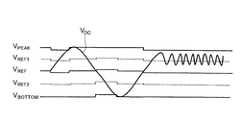
図2を参照して、第1アナログ検出信号Va及び第2アナログ検出信号Vbの位相差と振幅の関係を説明する。横軸は、第1アナログ検出信号Vaと第2アナログ検出信号Vbの位相差であり、縦軸は第1アナログ検出信号Va及び第2アナログ検出信号Vbの振幅を示している。この図に示される数値は一例であり、磁気センサ20a,20bや検出信号処理回路1の種類、磁気センサ20a,20bの配置位置が異なれば、これ以外の数値を取り得る。図2中の2A及び2Cは、回転体が微振動したときの第1アナログ検出信号Vaと第2アナログ検出信号Vbを示している。回転体が微振動したときの第1アナログ検出信号Vaと第2アナログ検出信号Vbは、位相差がほぼ0°又は180°であり、振幅の大きさは50mVよりも小さい。図2中の2Bは、回転体が正回転又は逆回転したときの第1アナログ検出信号Vaと第2アナログ検出信号Vbを示している。回転体が正回転又は逆回転したときの第1アナログ検出信号Vaと第2アナログ検出信号Vbは、位相差がほぼ60°〜90°の範囲内であり、振幅の大きさは10mV〜100mVである。 With reference to FIG. 2, the relationship between the phase difference and the amplitude of the first analog detection signal Va and the second analog detection signal Vb will be described. The horizontal axis represents the phase difference between the first analog detection signal Va and the second analog detection signal Vb, and the vertical axis represents the amplitude of the first analog detection signal Va and the second analog detection signal Vb. The numerical values shown in this figure are examples, and other numerical values can be taken if the types of the
図2の説明図から明らかなように、第1アナログ検出信号Vaと第2アナログ検出信号Vbの振幅が10mVよりも小さい場合、その信号は回転体の微振動に基づいて発生したものと判定することができる。一方、第1アナログ検出信号Vaと第2アナログ検出信号Vbの振幅が50mVよりも大きい場合、その信号は回転体の正回転又は逆回転に基づいて発生したものと判定することができる。 As is clear from the explanatory diagram of FIG. 2, when the amplitudes of the first analog detection signal Va and the second analog detection signal Vb are smaller than 10 mV, it is determined that the signals are generated based on the slight vibration of the rotating body. be able to. On the other hand, when the amplitudes of the first analog detection signal Va and the second analog detection signal Vb are larger than 50 mV, it can be determined that the signals are generated based on forward rotation or reverse rotation of the rotating body.
また、30°の位相差を第1閾値とし、150°の位相差を第2閾値とすると、位相差が30°〜150°の範囲外の第1アナログ検出信号Vaと第2アナログ検出信号Vbは、回転体の微振動に基づいて発生したものと判定することができる。また、位相差が30°〜150°の範囲内の第1アナログ検出信号Vaと第2アナログ検出信号Vbは、回転体の正回転又は逆回転に基づいて発生したものと判定することができる。 Also, assuming that the phase difference of 30 ° is the first threshold value and the phase difference of 150 ° is the second threshold value, the first analog detection signal Va and the second analog detection signal Vb whose phase difference is outside the range of 30 ° to 150 °. Can be determined to have occurred based on the slight vibration of the rotating body. Further, it can be determined that the first analog detection signal Va and the second analog detection signal Vb having a phase difference in the range of 30 ° to 150 ° are generated based on forward rotation or reverse rotation of the rotating body.
図3に、マスク制御回路78の回路構成の具体例の一例を示す。マスク制御回路78は、2つのAND回路71A,71Bと、OR回路73と、AND回路75を備えている。AND回路75はマスク制御信号を出力しており、そのマスク制御信号はマスク回路50に入力している。AND回路75のマスク制御信号がハイ信号のとき、マスク回路50は、正回転信号Sa1及び逆回転信号Sa2の通過を許可する。AND回路75のマスク制御信号がロー信号のとき、マスク回路50は、正回転信号Sa1及び逆回転信号Sa2の通過を許可しない。 FIG. 3 shows an example of a specific example of the circuit configuration of the
図中72の端子は、反転判定回路72の出力端子を示す。反転判定回路72の出力(反転停止要求信号の一例)は、AND回路75に入力している。反転判定回路72は、回転体が正回転又は逆回転しているときにハイ信号を出力し、回転体が正回転から逆回転、及び逆回転から正回転に反転したと判定したときにロー信号を出力する。 A terminal 72 in the figure indicates an output terminal of the
図中74の端子は、位相差判定回路74の出力端子を示す。位相差判定回路74の出力(位相差停止要求信号の一例)は、OR回路73に入力している。位相差判定回路74は、第1二値化検出信号Saと第2二値化検出信号Sbの位相差が30°〜150°の範囲内のときにハイ信号を出力し、位相差が30°〜150°の範囲外のときにロー信号を出力する。 A terminal 74 in the figure indicates an output terminal of the phase
図中76の上側端子76U(Va)は、第1アナログ検出信号Vaの振幅が50mVよりも大きい場合にハイ信号を出力し、50mV以下の場合にロー信号を出力する出力端子を示す。図中76の上側端子76U(Vb)は、第2アナログ検出信号Vbの振幅が50mVよりも大きい場合にハイ信号を出力し、50mV以下の場合にロー信号を出力する出力端子を示す。これら出力は、AND回路71Bを経由してOR回路73に入力している。このため、第1アナログ検出信号Vaと第2アナログ検出信号Vbの双方の振幅が50mVよりも大きい場合にハイ信号がOR回路73に入力し、少なくとも第1アナログ検出信号Vaと第2アナログ検出信号Vbのいずれか一方の振幅が50mV以下の場合にロー信号がOR回路73に入力する。 An
図中76の下側端子76D(Va)は、第1アナログ検出信号Vaの振幅が10mVよりも大きい場合にハイ信号を出力し、10mV以下の場合にロー信号を出力する出力端子を示す。図中76の下側端子76D(Vb)は、第2アナログ検出信号Vbの振幅が10mVよりも大きい場合にハイ信号を出力し、10mV以下の場合にロー信号を出力する出力端子を示す。これら出力は、AND回路71Aを経由してAND回路75に入力している。このため、AND回路71Aの出力(振幅停止要求信号の一例)は、第1アナログ検出信号Vaと第2アナログ検出信号Vbの双方の振幅が10mVよりも大きい場合にハイ信号となり、少なくとも第1アナログ検出信号Vaと第2アナログ検出信号Vbのいずれか一方の振幅が10mV以下の場合にロー信号となる。 A
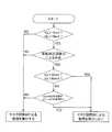
図4に、図3のマスク制御回路78の論理フローチャートを示す。まず、第1アナログ検出信号Vaと第2アナログ検出信号Vbの振幅が振幅判定回路76によって判定される。第1アナログ検出信号Vaと第2アナログ検出信号Vbの双方の振幅が10mVよりも大きい場合には、次の反転判定回路72による判定に進む。少なくとも第1アナログ検出信号Vaと第2アナログ検出信号Vbのいずれか一方の振幅が10mV以下の場合には、その信号は回転体の振動に基づくものであると判定され、正回転信号Sa1及び逆回転信号Sa2は、マスク回路50によってその通過が許可されない。 FIG. 4 shows a logic flowchart of the
次に、反転判定回路72によって回転体が正回転から逆回転、又は逆回転から正回転に反転したか否かが判定される。回転体が正回転から逆回転、又は逆回転から正回転に反転したと判定された場合には、反転した後の最初の正回転信号Sa1及び逆回転信号Sa2が、マスク回路50によってその通過が許可されない。回転体が正回転又は逆回転を続けている場合には、次の振幅判定回路76による判定に進む。 Next, it is determined by the
第1アナログ検出信号Vaと第2アナログ検出信号Vbの振幅が振幅判定回路76によって再度判定される。第1アナログ検出信号Vaと第2アナログ検出信号Vbの双方の振幅が50mVよりも大きい場合には、その信号が回転体の正回転又は逆回転に基づくものであると判定され、マスク回路50は、正回転信号Sa1及び逆回転信号Sa2の通過を許可する。少なくとも第1アナログ検出信号Vaと第2アナログ検出信号Vbのいずれか一方の振幅が50mV以下の場合には、次の位相差判定回路74による判定に進む。 The amplitudes of the first analog detection signal Va and the second analog detection signal Vb are determined again by the
第1二値化検出信号Saと第2二値化検出信号Sbの位相差が位相差判定回路74によって判定される。第1二値化検出信号Saと第2二値化検出信号Sbの位相差が30°〜150°の範囲内の場合には、その信号が回転体の正回転又は逆回転に基づくものであると判定され、マスク回路50は、正回転信号Sa1及び逆回転信号Sa2の通過を許可する。第1二値化検出信号Saと第2二値化検出信号Sbの位相差が30°〜150°の範囲外の場合には、その信号は回転体の振動に基づくものであると判定され、正回転信号Sa1及び逆回転信号Sa2は、マスク回路50によってその通過が許可されない。 The phase
このように、本実施例の検出信号処理回路10は、反転判定回路72と位相差判定回路74と振幅判定回路76とマスク制御回路78を利用することによって、図2に示す第1アナログ検出信号Saと第2アナログ検出信号Sbの位相差と振幅の差異に基づいた判定を実行することができる。これらの判定回路を利用することによって、出力信号の誤生成を抑制することができる。 As described above, the detection
上記の図4に示す論理フローチャートは、振幅判定回路76が10mVと50mVの2つの閾値を利用して判定する例である。他の実施例では、振幅判定回路76が1つの閾値を利用することも可能である。図5に、振幅判定回路76が1つの閾値を利用する場合のマスク制御回路78の回路構成の具体例の一例を示す。図6に、そのマスク制御回路78の論理フローチャートを示す。 The logic flowchart shown in FIG. 4 is an example in which the
図5に示すマスク制御回路78では、振幅判定回路76が10mVの閾値を利用する。振幅判定回路76は、少なくとも第1アナログ検出信号Vaと第2アナログ検出信号Vbのいずれか一方の振幅が10mV以下の場合には、その信号は回転体の振動に基づくものであると判定し、AND回路71Aの出力(振幅停止要求信号)をロー信号にする。振幅判定回路76では、第1アナログ検出信号Vaと第2アナログ検出信号Vbの双方の振幅が10mVよりも大きい場合には、AND回路71Aの出力がハイ信号となる。このようなマスク制御回路78でも、出力信号の誤生成を抑制することができる。 In the
以下、本実施例の検出信号処理回路10に用いられており、従来から知られていない特有な回路構成を説明する。しかし、以下に示す回路構成は、本発明の技術思想を具現化するための一つの態様であり、本発明の技術範囲はこの態様に限られるものではない。 Hereinafter, a specific circuit configuration that is used in the detection
(変換回路30a,30b)
図7に、第1変換回路30aの回路構成を例示する。なお、第2変換回路30bも同様の回路構成を備えている。したがって、以下の実施例では、第1変換回路30aを例に挙げて説明する。第1変換回路30aは、DC増幅回路38と、正のピーク電圧検出回路32と、負のピーク電圧検出回路34と、高精度ヒステリシスコンパレータ回路36を備えている。DC増幅回路38は、第1アナログ検出信号Vaを増幅して増幅第1アナログ検出信号VDCを生成する。正のピーク電圧検出回路32は、増幅第1アナログ検出信号VDCの正のピーク電圧を検出する。負のピーク電圧検出回路34は、増幅第1アナログ検出信号VDCの負のピーク電圧を検出する。高精度ヒステリシスコンパレータ回路36は、正のピーク電圧検出回路32で得られた正のピーク電圧と負のピーク電圧検出回路34で得られた負のピーク電圧から算出される閾値を利用して、増幅第1アナログ検出信号VDCを第1二値化検出信号Saに変換する。また、高精度ヒステリシスコンパレータ回路36は、後述するように、位相差判定回路74で用いられる遅延第1二値化検出信号S’aを生成することもできる。なお、前記したように、第2変換回路30bも同様の回路構成を備えており、第2変換回路30bは、第2二値化検出信号Sbと、位相差判定回路74で用いられる遅延第2二値化検出信号S’bを生成する。(
FIG. 7 illustrates a circuit configuration of the
第1変換回路30aで用いられている正のピーク電圧検出回路32は、変動する増幅第1アナログ検出信号VDCに追随して正のピーク電圧を検出する。正のピーク電圧検出回路32は、例えば、増幅第1アナログ検出信号VDCが環境温度の変化に応じて上昇又は下降したとしても、その変化に追随して正のピーク電圧を検出することができる。The positive peak
第1変換回路30aで用いられている負のピーク電圧検出回路34は、変動する増幅第1アナログ検出信号VDCに追随して負のピーク電圧を検出する。負のピーク電圧検出回路34は、例えば、増幅第1アナログ検出信号VDCが温度変化に応じて上昇又は下降したとしても、その変化に追随して負のピーク電圧を検出することができる。The negative peak
高精度ヒステリシスコンパレータ回路36は、高側オフセット閾値電圧と低側オフセット閾値電圧の間で比較閾値電圧を切換えて増幅アナログ検出信号VDCを第1二値化検出信号Saに変換する。さらに、高精度ヒステリシスコンパレータ回路36は、高側オフセット閾値電圧と低側オフセット閾値電圧を利用することによって生じる時間遅れを補償する回路を備えている。これにより、高精度ヒステリシスコンパレータ回路36は、増幅第1アナログ検出信号VDCを高精度に第1二値化検出信号Saに変換することができる。The high accuracy
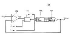
図8に、正のピーク電圧検出回路32の回路構成要素を具体的に示す。正のピーク電圧検出回路32は、コンパレータ131と、アンド回路132と、カウンタ回路133と、D/A変換回路134と、第1クロック信号発生回路と、第2クロック信号発生回路を備えている。第1クロック信号発生回路が生成する第1クロック信号CLK1の周期は、第2クロック信号発生回路が生成する第2クロック信号CLK2の周期よりも短い。第1クロック信号CLK1と第2クロック信号CLK2の周波数は、適宜に調整可能である。 FIG. 8 specifically shows circuit components of the positive peak
コンパレータ131は、非反転入力端子に増幅第1アナログ検出信号VDCが入力しており、反転入力端子にD/A変換回路134の出力電圧VPEAKが入力している。In the
アンド回路132は、2つの入力端子を備えており、一方の入力端子にコンパレータ131の出力信号VUPが入力しており、他方の入力端子に第1クロック信号CLK1が入力している。アンド回路132は、コンパレータ131の出力信号VUPがハイ信号のときにCLK1に同期した出力信号を出力する。AND
カウンタ回路133は、UP/DOWNのnビットカウンタ回路である。カウンタ回路133のUP用の入力端子には、アンド回路132の出力信号が入力している。カウンタ回路133のDOWN用の入力端子には、第2クロック信号CLK2が入力している。カウンタ回路133はさらに、RESET用の入力端子も備えており、そのRESET用の入力端子にリセット信号RSTが入力している。カウンタ回路133は、アンド回路132を利用して、コンパレータ131の出力信号VUPがハイ信号のときに第1クロック信号CLK1に同期してカウンタ値を加算する。正確には、第1クロック信号CLK1が正に反転するタイミングに同期してカウンタ値を加算する。カウンタ回路133はさらに、第2クロック信号CLK2に同期してカウンタ値を減算する。正確には、第2クロック信号CLK2が正に反転するタイミングに同期してカウンタ値を減算する。The
D/A変換回路134は、カウンタ回路133のカウンタ値に対応する電圧を出力する。D/A変換回路134の出力は、増幅アナログ検出信号VDCの正のピーク電圧VPEAKとして用いられるとともに、コンパレータ131の反転入力端子にも入力している。The D /
図9に、ピーク電圧検出回路32の動作波形図を示す。期間T1と期間T2は、ピーク電圧検出回路32が初期状態から増幅第1アナログ検出信号VDCの正のピーク電圧を検出するまでの過渡期間である。期間T3と期間T5は、増幅第1アナログ検出信号VDCの正のピーク電圧を検出する過程の期間である。期間T4は、検出した正のピーク電圧の波から次の波が現れるまでの期間である。期間T4は、ピーク電圧検出回路32の特徴が最も現れている期間である。FIG. 9 shows an operation waveform diagram of the peak
まず、期間T1と期間T2に関して説明する。ピーク電圧検出回路32の測定が開始すると、リセット信号RSTがカウンタ回路133に入力し、カウンタ回路133のカウンタ値が初期化される。カウンタ回路133のカウンタ値が初期化されると、D/A変換回路134の出力電圧VPEAKも初期化される。カウンタ値の初期値は低く設定されているので、出力電圧VPEAKの初期電圧も小さい。カウンタ値の初期値は、出力電圧VPEAKが増幅第1アナログ検出信号VDCを下回るように設定されている。このため、測定開始時の増幅第1アナログ検出信号VDCは、出力電圧VPEAKを上回っており、コンパレータ131の出力信号VUPがハイ信号になる。アンド回路132は、コンパレータ131の出力信号VUPがハイ信号であるときに、第1クロック信号CLK1をカウンタ回路134に入力する。カウンタ回路134は、第1クロック信号CLK1に同期してカウンタ値を加算する。これにより、D/A変換回路134の出力電圧VPEAKは、第1クロック信号CLK1に同期して段差状に上昇する(期間T1)。First, the period T1 and the period T2 will be described. When the measurement of the peak
タイミングt1において、出力電圧VPEAKが増幅第1アナログ検出信号VDCまで達し、出力電圧VPEAKが増幅第1アナログ検出信号VDCを上回ると、コンパレータ131の出力信号VUPがロー信号になる。アンド回路132は、第1クロック信号CLK1をカウンタ回路133に入力するのを停止する。したがって、カウンタ回路133は、第1クロック信号CLK1に同期したカウンタ値の加算を停止する。この結果、出力電圧VPEAKの上昇も停止する。ここで、カウンタ回路133のDOWN用の入力端子には、第2クロック信号CLK2が入力している。このため、カウンタ回路133のカウンタ値は、第2クロック信号CLK2に同期して減算する。したがって、期間T2では、出力電圧VPEAKが第2クロック信号CLK2に同期して下降する。At timing t1, when the output voltage VPEAK reaches the amplified first analog detection signal VDC and the output voltage VPEAK exceeds the amplified first analog detection signal VDC , the output signal VUP of the
タイミングt2において、増幅第1アナログ検出信号VDCが出力電圧VPEAKを上回ると、増幅第1アナログ検出信号VDCの正のピーク電圧を検出する過程に入る(期間T3)。増幅第1アナログ検出信号VDCが出力電圧VPEAKを上回っていると、コンパレータ131の出力信号VUPがハイ信号になる。アンド回路132は、コンパレータ131の出力信号VUPがハイ信号であるときに、第1クロック信号CLK1をカウンタ回路133に入力する。カウンタ回路133は、第1クロック信号CLK1に同期してカウンタ値を加算する。これにより、D/A変換回路134の出力電圧VPEAKは、第1クロック信号CLK1に同期して段差状に上昇する。即ち、出力電圧VPEAKは、増幅第1アナログ検出信号VDCが出力電圧VPEAKを上回っているときに、第1クロック信号CLK1に同期して段差状に上昇し、増幅第1アナログ検出信号VDCの上昇に追随していく。この期間T3でも、カウンタ回路134のカウンタ値は、第2クロック信号CLK2に同期して減算する。しかし、第2クロック信号CLK2の周期は、第1クロック信号CLK1の周期よりも極めて長い。このため、第2クロック信号CLK2に基づくカウンタ値の減算分は、第1クロック信号CLK1に基づく加算分によって実質的に無視することができる。したがって、出力電圧VPEAKは、第1クロック信号CLK1に同期して段差状に上昇し、増幅アナログ検出信号VDCの上昇に追随していくことができる。When the amplified first analog detection signal VDC exceeds the output voltage VPEAK at timing t2, the process enters a process of detecting the positive peak voltage of the amplified first analog detection signal VDC (period T3). When the amplified first analog detection signal VDC exceeds the output voltage VPEAK , the output signal VUP of the
タイミングt3において、増幅第1アナログ検出信号VDCが下降し始めると、増幅第1アナログ検出信号VDCが出力電圧VPEAKを下回る。増幅第1アナログ検出信号VDCが出力電圧VPEAKを下回ると、コンパレータ131の出力信号VUPがロー信号になり、カウンタ回路133に第1クロック信号CLK1が入力しない。したがって、カウンタ回路133は、カウンタ値の加算を停止する。これらの処理を経て、ピーク電圧検出回路32は、増幅アナログ検出信号VDCの正のピーク値を検出する。At timing t3, when the amplified first analog detection signalV DC starts to descend, amplified first analog detection signalV DC is lower than the output voltageV PEAK. When the amplified first analog detection signal VDC falls below the output voltage VPEAK , the output signal VUP of the
期間T4では、カウンタ回路133のカウンタ値が、第2クロック信号CLK2に同期して減算する。このため、保持されている出力電圧VPEAKは、次の周期の増幅第1アナログ検出信号VDCが現れるまで段差状に下降する。保持されている出力電圧VPEAKが徐々に下降するので、次の周期の波を確実に捉えることができる。増幅第1アナログ検出信号VDCが緩慢に減少していたとしても、確実に検出することができる。In the period T4, the counter value of the
次に、タイミングt4において、増幅第1アナログ検出信号VDCが出力電圧VPEAKを上回ると、増幅第1アナログ検出信号VDCの正のピーク電圧を検出する過程に入る(期間T5)。期間T5とタイミングt5における動作は、前記の期間T3とタイミングt5における動作と同一である。Next, when the amplified first analog detection signal VDC exceeds the output voltage VPEAK at timing t4, a process of detecting a positive peak voltage of the amplified first analog detection signal VDC is started (period T5). The operation in the period T5 and the timing t5 is the same as the operation in the period T3 and the timing t5.
図10に、増幅第1アナログ検出信号VDCの複数の周期を観測した様子を示す。増幅第1アナログ検出信号VDCは、急峻に変動する成分の他に、温度変化等に起因して緩慢に変動する成分も含まれている。このため、図10に示すように、増幅第1アナログ検出信号VDCは、緩慢に増加する期間T10と緩慢に減少する期間T20を備えている。図10に示すように、正のピーク電圧検出回路32は、緩慢に増加する期間T10と緩慢に減少する期間T20のいずれにおいても、増幅第1アナログ検出信号VDCの正のピーク電圧を周期毎に検出することができる。FIG. 10 shows a state in which a plurality of periods of the amplified first analog detection signalVDC are observed. The amplified first analog detection signalVDC includes a component that varies slowly due to a temperature change or the like in addition to a component that varies sharply. For this reason, as shown in FIG. 10, the amplified first analog detection signalVDC has a slowly increasing period T10 and a slowly decreasing period T20. As shown in FIG. 10, the positive peak
正のピーク電圧検出回路32は、増幅第1アナログ検出信号VDCが出力電圧VPEAKを上回っているときに、周期の短い第1クロック信号CLK1を利用して、カウンタ回路133のカウンタ値を加算させ、出力電圧VPEAKを上昇させることができる。したがって、出力電圧VPEAKは、増幅第1アナログ検出信号VDCの急峻な上昇に追随して上昇することができる。さらに、正のピーク電圧検出回路32は、周期の長い第2クロック信号CLK2を利用して、カウンタ回路133のカウンタ値を減算させ、出力電圧VPEAKを下降させることができる。したがって、出力電圧VPEAKは、増幅第1アナログ検出信号VDCの緩慢な下降に追随して下降することができる。When the amplified first analog detection signal VDC exceeds the output voltage VPEAK , the positive peak
正のピーク電圧検出回路32は、2つのクロック信号を利用することによって、正のピーク電圧VPEAKを増幅第1アナログ検出信号VDCの急峻な変動と緩慢な変動の双方に追随させることができる。正のピーク電圧検出回路32によると、増幅第1アナログ検出信号VDCの、正のピーク電圧VPEAKを正確に検出することができる。By using two clock signals, the positive peak
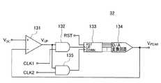
図11に、正のピーク電圧検出回路32の変形例の構成を示す。変形例の正のピーク電圧検出回路32は、第2のアンド回路135を備えている。第2のアンド回路135は、2つの入力端子を備えており、一方の入力端子にはコンパレータ131の出力信号VUPが反転した信号が入力しており、他方の入力端子には第2クロック信号CLK2が入力している。第2のアンド回路135は、コンパレータ131の出力信号VUPがロー信号のときに第2クロック信号CLK2に同期した出力信号を出力する。FIG. 11 shows a configuration of a modified example of the positive peak
変形例の正のピーク電圧検出回路32によると、カウンタ回路133は、コンパレータ131の出力信号VUPがローのときに、第2クロック信号CLK2に同期してカウンタ値を減算する。換言すると、変形例の正のピーク電圧検出回路32では、コンパレータ131の出力信号VUPがハイのときに(即ち、増幅第1アナログ検出信号VDCが出力電圧VPEAKを上回っているときに)、カウンタ回路133のカウンタ値が第2クロック信号CLK2に同期して減算することがない。したがって、変形例の正のピーク電圧検出回路32によると、増幅第1アナログ検出信号VDCが急峻に上昇する過程では、出力電圧VPEAKを増幅アナログ検出信号VDCの急峻な上昇に良好に追随させることができる。According to the positive peak
本実施例の正のピーク電圧検出回路32で検出される正のピーク電圧VPEAKは、第2クロック信号CLK2に同期して緩慢に変化する。緩慢とはいえ変化することから厳密な意味ではピーク電圧VPEAKを保持しているとはいえない。しかしながら第2クロック信号CLK2に同期する変化は緩慢であり、ピーク電圧VPEAKを近似的に保持しているといえる。また、後記する高精度ヒステリシスコンパレータ回路36に利用する場合、正のピーク電圧VPEAKを保持した電圧が緩慢に変化する方向(緩慢に低下する)と、負のピーク電圧VBOTTOMを保持した電圧が緩慢に変化する方向(緩慢に上昇する)が逆向きであり、緩慢に変化するにもかかわらず、正のピーク電圧VPEAKを保持した電圧と負のピーク電圧VBOTTOMを保持した電圧の中間値は変化しない。周期毎の中間値を正確に抽出することを妨げない。The positive peak voltage VPEAK detected by the positive peak
図12に、負のピーク電圧検出回路34の構成を示す。負のピーク電圧検出回路34の構成と正のピーク電圧検出回路32は、以下の2つの点で異なっている。 FIG. 12 shows the configuration of the negative peak
負のピーク電圧検出回路34では、コンパレータ231の反転入力端子に増幅第1アナログ検出信号VDCが入力しており、非反転入力端子にD/A変換回路234の出力電圧VBOTTOMが入力している。さらに、カウンタ回路233は、UP/DOWNのnビットカウンタ回路であり、その出力は反転してD/A変換回路234に入力している。In the negative peak
負のピーク検出回路34では、増幅第1アナログ検出信号VDCが出力電圧VBOTTOMを下回っているときに、コンパレータ231の出力信号VDOWNがハイになる。アンド回路232は、コンパレータ231の出力信号VDOWNがハイのときに、第1クロック信号CLK1をカウンタ回路233のUP用の入力端子に入力する。したがって、カウンタ回路233のカウンタ値は、増幅第1アナログ検出信号VDCが出力電圧VBOTTOMを下回っているときに、第1クロック信号CLK1に同期して加算する。ただし、カウンタ回路233の出力は反転している。このため、実質的には、カウンタ回路233のカウンタ値は、増幅第1アナログ検出信号VDCが出力電圧VBOTTOMを下回っているときに、第1クロック信号CLK1に同期して減算する。この結果、負のピーク検出回路34は、増幅第1アナログ検出信号VDCが出力電圧VBOTTOMを下回っているときに、第1クロック信号CLK1に同期して出力電圧VBOTTOMを下降させることができる。したがって、出力電圧VBOTTOMは、増幅第1アナログ検出信号VDCの急峻な下降に追随して下降することができる。さらに、負のピーク電圧検出回路34は、周期の長い第2クロック信号CLK2を利用して、カウンタ回路233のカウンタ値を減算する。ただし、上記したように、カウンタ回路233の出力は反転している。このため、カウンタ回路233のカウンタ値を実質的に加算させ、出力電圧VBOTTOMを上昇させることができる。したがって、出力電圧VBOTTOMは、増幅第1アナログ検出信号VDCの緩慢な上昇に追随して上昇することができる。In the negative
負のピーク電圧検出回路34は、2つのクロック信号を利用することによって、負のピーク電圧VBOTTOMを急峻な変動と緩慢な変動の双方に追随させることができる。負のピーク電圧検出回路34によると、増幅第1アナログ検出信号VDCの負のピーク電圧VBOTTOMを正確に検出することができる。The negative peak
図13に、負のピーク電圧検出回路34の変形例の構成を示す。変形例の負のピーク電圧検出回路34は、第2のアンド回路235を備えている。第2のアンド回路235は、2つの入力端子を備えており、一方の入力端子にはコンパレータ231の出力信号VDOWNが反転した信号が入力しており、他方の入力端子には第2クロック信号CLK2が入力している。FIG. 13 shows a configuration of a modified example of the negative peak
変形例の負のピーク電圧検出回路34によると、カウンタ回路233は、コンパレータ231の出力信号VDOWNがローのときのみ、第2クロック信号CLK2に同期してカウンタ値を実質的に加算する。換言すると、変形例の負のピーク電圧検出回路34では、コンパレータ231の出力信号VDOWNがハイのときに(即ち、増幅第1アナログ検出信号VDCが出力電圧VBOTTOMを上回っているときに)、カウンタ回路233のカウンタ値が第2クロック信号CLK2に同期して加算することがない。したがって、変形例の負のピーク電圧検出回路34によると、増幅第1アナログ検出信号VDCが急峻に下降する過程では、出力電圧VBOTTOMを増幅第1アナログ検出信号VDCの急峻な下降に良好に追随させることができる。According to the negative peak
図14に、第1変換回路30aの全体構成を示す。第1変換回路30aは、図8の正のピーク電圧検出回路32と、図12の負のピーク電圧検出回路34と、高精度ヒステリシスコンパレータ回路36と、DC増幅回路38を備えている。第1変換回路30aはさらに、クロック回路236と分周回路238を備えている。クロック回路236は、第1クロック信号CLK1を生成する。分周回路238は、高周波の第1クロック信号CLK1を低周波の第2クロック信号CLK2に変換する。 FIG. 14 shows the overall configuration of the
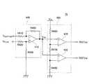
図15に、高精度ヒステリシスコンパレータ回路36の回路構成を具体的に示す。高精度ヒステリシスコンパレータ回路36は、正のピーク電圧VPEAKと負のピーク電圧VBOTTOMを利用して、基準閾値電圧VREFと、高側オフセット閾値電圧VREF1と、低側オフセット閾値電圧VREF2を生成する。図15に示すように、高精度ヒステリシスコンパレータ回路36は、第1比較回路90と、第2比較回路80と、第1フリップフロップ回路88と、第2フリップフロップ回路89と、4つの抵抗R10〜R40を備えている。なお、第2フリップフロップ回路89は、後述するように、遅延第1二値化検出信号S’aを生成するために用いられている。また、前記したように、第2変換回路30bの高精度ヒステリシスコンパレータ回路も同様の回路構成を備えており、第2変換回路30bの第2フリップフロップ回路は遅延第2二値化検出信号S’bを生成する。FIG. 15 specifically shows the circuit configuration of the high-precision
増幅第1アナログ検出信号VDCは、正のピーク電圧検出回路32と負のピーク電圧検出回路34に入力している。抵抗R10〜R40は、正のピーク電圧検出回路32の出力端子と負のピーク電圧検出回路34の出力端子の間に直列に設けられている。抵抗R10と抵抗R20の間に、第1接続端子30Hが形成されている。抵抗R20と抵抗R30の間に、第2接続端子30Mが形成されている。抵抗R30と抵抗R40の間に、第3接続端子30Dが形成されている。抵抗R10〜R40の抵抗値は同一である。したがって、各接続端子30H、30M、30Dの電圧は、以下の値に調整される。The amplified first analog detection signalVDC is input to the positive peak

第2接続端子30Mの電圧は、正のピーク電圧VPEAKと負のピーク電圧VBOTTOMの中心値に調整されており、この電圧は基準閾値電圧VREFとして用いられる。第1接続端子30Hの電圧は、基準閾値電圧VREFと正のピーク電圧VPEAKの中心値に調整されており、この電圧は高側オフセット閾値電圧VREF1として用いられる。第3接続端子30Dの電圧は、基準閾値電圧VREFと負のピーク電圧VBOTTOMの中心値に調整されており、この電圧は低側オフセット閾値電圧VREF2として用いられる。The voltage of the
第1比較回路90は、第1オペアンプ92と第1スイッチ切換回路94を備えている。第1オペアンプ92の非反転入力端子には、増幅第1アナログ検出信号VDCが入力している。第1スイッチ切換回路94は、第1オペアンプ92の出力に応じて、第1オペアンプ92の反転入力端子に接続する端子を、第1接続端子30Hと第2接続端子30Mの間で切替える。すなわち、第1スイッチ切換回路94は、第1オペアンプ92の出力に応じて、第1オペアンプ92の反転入力端子に入力する電圧を、高側オフセット閾値電圧VREF1と基準閾値電圧VREFの間で切換える。The
第1比較回路90は、増幅第1アナログ検出信号VDCが基準閾値電圧VREFを下回ったときに出力を正から負に反転させるとともに、比較閾値電圧を高側オフセット閾値電圧VREF1に切換える。また、第1比較回路90は、増幅第1アナログ検出信号VDCが高側オフセット閾値電圧VREF1を上回った時に出力を負から正に反転させるとともに、比較閾値電圧を基準閾値電圧VREFに切換える。The
第2比較回路80は、第2オペアンプ82と第2スイッチ切換回路84を備えている。第2オペアンプ82の非反転入力端子には、増幅第1アナログ検出信号VDCが入力している。第2スイッチ切換回路84は、第2オペアンプ82の出力に応じて、第2オペアンプ82の反転入力端子に接続する端子を、第2接続端子30Mと第3接続端子30Dの間で切替える。すなわち、第2スイッチ切換回路84は、第2オペアンプ82の出力に応じて、第2オペアンプ82の反転入力端子に入力する電圧を、基準閾値電圧VREFと低側オフセット閾値電圧VREF2の間で切換える。The
第2比較回路80は、増幅第1アナログ検出信号VDCが基準閾値電圧VREFを上回った時に出力を負から正に反転させるとともに、比較閾値電圧を低側オフセット閾値電圧VREF2に切換える。また、第2比較回路80は、増幅アナログ検出信号VDCが低側オフセット閾値電圧VREF2を下回った時に出力を正から負に反転させるとともに、比較閾値電圧を基準閾値電圧VREFに切換える。The
第1フリップフロップ回路88は、第1比較回路90と第2比較回路80の出力電圧を入力する。第1フリップフロップ回路88は、増幅第1アナログ検出信号VDCが基準閾値電圧VREFを下回った時に生じる第1比較回路90の出力反転現象(正から負)と、増幅第1アナログ検出信号VDCが基準閾値電圧VREFを上回った時に生じる第2比較回路80の出力反転現象(負から正)を選択して出力を反転させる。なお、第1オペアンプ92の出力は、反転した後に第1フリップフロップ回路88のリセット端子Rに入力している。第2オペアンプ82の出力は、反転しないで第1フリップフロップ回路88のセット端子Sに入力している。The first flip-
図16に、第1スイッチ切換回路94と第2スイッチ切換回路84の具体的な構成を示す。第1スイッチ切換回路94は、第1トランジスタ95と第2トランジスタ97を備えている。第1トランジスタ95は、第1オペアンプ92の反転入力端子と第1接続端子30Hの間に設けられている。第1トランジスタ95のゲートには、インバータ93によって反転された第1オペアンプ92の出力が入力している。第2トランジスタ97は、第1オペアンプ92の反転入力端子と第2接続端子30Mの間に設けられている。第2トランジスタ97のゲートには、インバータ93によって反転されていない第1オペアンプ92の出力が入力している。 FIG. 16 shows a specific configuration of the first
第2スイッチ切換回路84は、第3トランジスタ85と第4トランジスタ87を備えている。第3トランジスタ85は、第2オペアンプ82の反転入力端子と第2接続端子30Mの間に設けられている。第3トランジスタ85のゲートには、インバータ83によって反転された第2オペアンプ82の出力が入力している。第4トランジスタ87は、第2オペアンプ82の反転入力端子と第3接続端子30Dの間に設けられている。第4トランジスタ87のゲートには、インバータ83によって反転されていない第2オペアンプ82の出力が入力している。 The second
図16と図17を参照して、高精度ヒステリシスコンパレータ回路36の動作について説明する。なお、説明の簡単化のため、正のピーク電圧VPEAKと負のピーク電圧VBOTTOMが一定の場合について説明する。The operation of the high-precision
まず、第1比較回路90の動作について説明する。第1トランジスタ95と第2トランジスタ97は、双方ともゲートに正の電圧が印加されるとオンするトランジスタである。増幅第1アナログ検出信号VDCが高側オフセット閾値電圧VREF1を上回る直前までは、第1オペアンプ92の反転入力端子に高側オフセット閾値電圧VREF1が入力されており、第1オペアンプ92の非反転入力端子に増幅アナログ検出信号VDCが入力されている。増幅第1アナログ検出信号VDCが高側オフセット閾値電圧VREF1を上回った時(t12、t16)に、第1オペアンプ92の出力がハイに切換わる。第1オペアンプ92の出力電圧は、インバータ93によって反転され、第1トランジスタ95のゲートに負の電圧が入力される。第1トランジスタ95がオフする。さらに、第1オペアンプ92の出力電圧は、インバータ93によって反転されないで、第2トランジスタ97のゲートに印加される。この結果、第2トランジスタ97のゲートに正の電圧が入力される。第2トランジスタ97がオンする。第1オペアンプ92の反転入力端子に基準閾値電圧VREFが入力される。First, the operation of the
増幅第1アナログ検出信号VDCが基準閾値電圧VREFを下回った時(t13、t17)、第1オペアンプ92の出力がローに切換わる。第1オペアンプ92の出力電圧は、インバータ93によって反転されるので、第1トランジスタ95のゲートに正の電圧が入力される。第1トランジスタ95がオンする。さらに、第1オペアンプ92の出力電圧は、インバータ93によって反転されないで、第2トランジスタ97のゲートに印加される。この結果、第2トランジスタ97のゲートに負の電圧が入力される。第2トランジスタ97がオフする。第1オペアンプ92の反転入力端子に高側オフセット閾値電圧VREF1が入力される。When the amplified first analog detection signal VDC falls below the reference threshold voltage VREF (t13, t17), the output of the first
次に、第2比較回路80の動作について説明する。第3トランジスタ85と第4トランジスタ87は、双方ともゲートに正の電圧が印加されるとオンするトランジスタである。増幅第1アナログ検出信号VDCが基準閾値電圧VREFを上回る直前までは、第2オペアンプ82の反転入力端子に基準閾値電圧VREFが入力されており、第2オペアンプ82の非反転入力端子に増幅第1アナログ検出信号VDCが入力されている。増幅第1アナログ検出信号VDCが基準閾値電圧VREFを上回った時(t11、t15)に、第2オペアンプ82の出力がハイに切換わる。第2オペアンプ82の出力電圧は、インバータ83によって反転されるので、第3トランジスタ85のゲートに負の電圧が入力される。第3トランジスタ85がオフする。さらに、第2オペアンプ82の出力電圧は、インバータ83によって反転されないで、第4トランジスタ87のゲートに印加される。この結果、第4トランジスタ87のゲートに正の電圧が入力される。第4トランジスタ87がオンする。第2オペアンプ82の反転入力端子に低側オフセット閾値電圧VREF2が入力される。Next, the operation of the
増幅第1アナログ検出信号VDCが低側オフセット閾値電圧VREF2を下回った時(t14、t18)、第2オペアンプ82の出力がローに切換わる。第2オペアンプ82の出力電圧は、インバータ83によって反転されるので、第3トランジスタ85のゲートに正の電圧が入力される。第3トランジスタ85がオンする。さらに、第2オペアンプ82の出力電圧は、インバータ83によって反転されないで、第4トランジスタ87のゲートに印加される。この結果、第4トランジスタ87のゲートに負の電圧が入力される。第4トランジスタ87がオフする。第2オペアンプ82の反転入力端子に基準閾値電圧VREFが入力される。When the amplified first analog detection signal VDC falls below the low-side offset threshold voltage VREF2 (t14, t18), the output of the second
上記したように、第1比較回路90の働きによって、増幅第1アナログ検出信号VDCが高側オフセット閾値電圧VREF1を上回った時t12、t16に、閾値電圧が基準閾値電圧VREFに切り換わる。増幅第1アナログ検出信号VDCが基準閾値電圧VREFを下回った時t13、t17に、閾値電圧が高側オフセット閾値電圧VREF1に切り換わる。図17(A)に示すように、第1比較回路90が比較対象とする閾値電圧が、電圧レベル192のようにステップ状に変化する。As described above, the threshold voltage is switched to the reference threshold voltage VREF at t12 and t16 when the amplified first analog detection signal VDC exceeds the high-side offset threshold voltage VREF1 by the action of the
図17(B)は、第1比較回路90の出力がインバータ93によって反転した後の出力VA(第1フリップフロップ回路88のリセット端子Rに入力する信号)を示している。増幅第1アナログ検出信号VDCが高側オフセット閾値電圧VREF1を上回った時t12、t16に正から負に反転し、増幅アナログ検出信号VDCが基準閾値電圧VREFを下回った時t13、t17に負から正に反転する。FIG. 17B shows an output VA (signal input to the reset terminal R of the first flip-flop circuit 88) after the output of the
第2比較回路80の働きによって、増幅第1アナログ検出信号VDCが基準閾値電圧VREFを上回った時t11、t15に、閾値電圧が低側オフセット閾値電圧VREF2に切り換わる。増幅第1アナログ検出信号VDCが低側オフセット閾値電圧VREF2を下回った時t14、t18に、閾値電圧が基準閾値電圧VREFに切り換わる。図17(A)に示すように、第2比較回路80が比較対象とする閾値電圧が、電圧レベル194のようにステップ状に変化する。By the action of the
図17(C)は、第2比較回路80の出力VB(第1フリップフロップ回路88のセット端子Sに入力する信号)を示している。増幅第1アナログ検出信号VDCが基準閾値電圧VREFを上回った時t11、t15に負から正に反転し、増幅アナログ検出信号VDCが低側オフセット閾値電圧VREF2を下回った時t14、t18に正から負に反転する。FIG. 17C shows the output VB of the second comparison circuit 80 (signal input to the set terminal S of the first flip-flop circuit 88). When the amplified first analog detection signal VDC exceeds the reference threshold voltage VREF, it is inverted from negative to positive at t11 and t15, and when the amplified analog detection signal VDC falls below the low-side offset threshold voltage VREF2 , t14 and t18. Invert from positive to negative.
第1フリップフロップ回路88のリセット端子Rには、第1比較回路90の出力電圧が反転されて入力されている(図17(B)の電圧VAが入力されている)。図17(B)に示す出力電圧VAが負から正に反転するタイミング(t13、t17)において、第1フリップフロップ回路88の出力Saの電圧を正から負に反転させる。また、セット端子Sには第2比較回路80の出力VBが反転されないで入力されている。図17(C)に示す出力VBが負から正に反転するタイミング(t11、t15)において、フリップフロップ回路88の出力Saの電圧を負から正に反転させる。この結果、図17(D)に示す第1二値化検出信号Saが得られる。第1二値化検出信号Saは、増幅第1アナログ検出信号VDCが基準閾値電圧VREFを上回った時t11、t15に負から正に反転し、増幅第1アナログ検出信号VDCが基準閾値電圧VREFを下回った時t13、t17に正から負に反転する。The output voltage of the
高精度ヒステリシスコンパレータ回路36によると、正のピーク電圧VPEAKと負のピーク電圧VBOTTOMを利用して高側オフセット閾値電圧VREF1と低側オフセット閾値電圧VREF2を生成する。このため、高側オフセット閾値電圧VREF1と低側オフセット閾値電圧VREF2が、脈動する増幅第1アナログ検出信号VDCの振幅に応じて変動することができる。According to the high-precision
磁気センサ20a,20bから得られるアナログ検出信号Va,Vbは、その振幅が温度変化によって大きく変化することが知られている。高側オフセット閾値電圧VREF1と低側オフセット閾値電圧VREF2が固定されている場合、アナログ検出信号Va,Vbが、高側オフセット閾値電圧VREF1と低側オフセット閾値電圧VREF2を超えることができない事態が発生してしまう。この場合、脈動するアナログ検出信号Va,Vbを正確に二値化検出信号Sa,Sbに変換することができなくなってしまう。一方、高精度ヒステリシスコンパレータ回路36によると、高側オフセット閾値電圧VREF1と低側オフセット閾値電圧VREF2は、脈動するアナログ検出信号Va,Vbの振幅が小さくなったとしても、それに応じて調整されるので脈動するアナログ検出信号Va,Vbを正確に二値化検出信号Sa,Sbに変換することができる。It is known that the amplitudes of the analog detection signals Va and Vb obtained from the
しかしながら、このような高精度ヒステリシスコンパレータ回路36を利用すると、回転体が微振動したときに誤作動するという問題がある。図18に、回転体が正回転又は逆回転している状態から微振動に移行したときの増幅第1アナログ検出信号VDCの様子を示す。前記したピーク検出回路32,34と高精度ヒステリシスコンパレータ回路36を組み合わせた変換回路30a,30bを用いた場合、時間が経過すると、回転体が微振動したときの増幅第1アナログ検出信号VDCのピーク電圧を検出し、二値化検出信号Sa,Sbを出力することになる。この場合、従来の検出信号処理回路では、図29〜図31に示したように、回転体が正回転又は逆回転していると誤判定してしまう。しかし、前記したように、本実施例の検出信号処理回路10は、反転判定回路72と位相差判定回路74と振幅判定回路76とマスク制御回路78を利用することにより、この種の振動による出力信号の誤生成を抑制することができる。本実施例の検出信号処理回路10は、この種の変換回路30a,30bが微振動によって誤作動することを改善できる。この点において、本実施例の検出信号処理回路10は、特に有用な結果を提供するものである。However, when such a high-precision
(位相差判定回路74)
図19及び図20を参照して、位相差判定回路74の判定方法を説明する。図19は、回転体が微振動したときに出力される二値化検出信号Sa,Sbの位相差が0°の場合(図31のSP1参照)を考慮した判定方法を説明している。図20は、回転体が微振動したときに出力される二値化検出信号Sa,Sbの位相差が180°の場合(図31のSP2参照)を考慮した判定方法を説明している。(Phase difference determination circuit 74)
The determination method of the phase
位相差判定回路74は、第1二値化検出信号Saを遅延させた遅延第1二値化検出信号S’aと、第2二値化検出信号Sbを遅延させた遅延第2二値化検出信号S’bと、遅延第2二値化検出信号S’bを反転させた反転遅延第2二値化検出信号S’brを利用する。遅延第1二値化検出信号S’aと遅延第2二値化検出信号S’bは、高精度ヒステリシスコンパレータ回路36を用いて生成することができる。反転遅延第2二値化検出信号S’brは、遅延第2二値化検出信号S’bをインバータで反転させることによって生成することができる。遅延第1二値化検出信号S’aと遅延第2二値化検出信号S’bの生成に係る詳細は後述する。 The phase
図19(A)は、回転体が正回転している例である。図19(A)の右図に示すように、回転体が正回転している場合、第1二値化検出信号Saのレベル変化から例えば60°〜90°の位相差を有して第2二値化検出信号Sbのレベル変化が生じる。遅延第1二値化検出信号S’aがレベル変化するタイミングにおいて、第1二値化検出信号Saがハイであり、第2二値化検出信号Sbがローであれば、回転体が正回転していると判定することができる。一方、図19(A)の左図に示すように、遅延第1二値化検出信号S’aがレベル変化するタイミングにおいて、第1二値化検出信号Sa及び第2二値化検出信号Sbの双方がハイであれば、回転体が微振動していると判定することができる。 FIG. 19A shows an example in which the rotating body is rotating forward. As shown in the right diagram of FIG. 19A, when the rotating body is rotating in the forward direction, a second phase difference of, for example, 60 ° to 90 ° is obtained from the level change of the first binarization detection signal Sa. A level change of the binarization detection signal Sb occurs. If the first binarization detection signal Sa is high and the second binarization detection signal Sb is low at the timing when the level of the delayed first binarization detection signal S′a changes, the rotating body rotates forward. Can be determined. On the other hand, as shown in the left diagram of FIG. 19A, at the timing when the level of the delayed first binarization detection signal S′a changes, the first binarization detection signal Sa and the second binarization detection signal Sb. If both are high, it can be determined that the rotating body is slightly vibrating.
図19(B)は、回転体が逆回転している例である。図19(B)の右図に示すように、回転体が逆回転している場合、第2二値化検出信号Sbのレベル変化から例えば60°〜90°の位相差を有して第1二値化検出信号Saのレベル変化が生じる。遅延第2二値化検出信号S’bがレベル変化するタイミングにおいて、第2二値化検出信号Sbがハイであり、第1二値化検出信号Saがローであれば、回転体が逆回転していると判定することができる。一方、図19(B)の左図に示すように、遅延第2二値化検出信号S’bがレベル変化するタイミングにおいて、第2二値化検出信号Sb及び第1二値化検出信号Saの双方がハイであれば、回転体が微振動していると判定することができる。 FIG. 19B shows an example in which the rotating body rotates in the reverse direction. As shown in the right diagram of FIG. 19B, when the rotator is rotating in the reverse direction, the first difference with a phase difference of, for example, 60 ° to 90 ° from the level change of the second binarization detection signal Sb. A level change of the binarization detection signal Sa occurs. If the second binarization detection signal Sb is high and the first binarization detection signal Sa is low at the timing when the delayed second binarization detection signal S′b changes in level, the rotating body rotates in reverse. Can be determined. On the other hand, as shown in the left diagram of FIG. 19B, at the timing when the level of the delayed second binarization detection signal S′b changes, the second binarization detection signal Sb and the first binarization detection signal Sa. If both are high, it can be determined that the rotating body is slightly vibrating.
前記したように、図20は、回転体が微振動したときに出力される二値化検出信号Sa,Sbの位相差が180°の例である。この例では、第2二値化検出信号Sbを反転させた反転第2二値化検出信号Sbrを生成することによって、図19と同様の判定方法を利用して位相差の判定を実施することができる。なお、反転第2二値化検出信号Sbrに代えて、第1二値化検出信号Saを反転させた反転第1二値化検出信号を利用することが可能なことは、同業者であれば容易に理解できるであろう。 As described above, FIG. 20 is an example in which the phase difference between the binarization detection signals Sa and Sb output when the rotating body slightly vibrates is 180 °. In this example, the phase difference is determined using the same determination method as in FIG. 19 by generating the inverted second binarization detection signal Sbr obtained by inverting the second binarization detection signal Sb. Can do. Note that it is possible to use an inverted first binarization detection signal obtained by inverting the first binarization detection signal Sa instead of the inverted second binarization detection signal Sbr. It will be easy to understand.
図20(A)は、回転体が正回転している例である。図20(A)の右図に示すように、回転体が正回転している場合、反転第2二値化検出信号Sbrのレベル変化から例えば60°〜90°の位相差を有して第1二値化検出信号Saのレベル変化が生じる。反転遅延第2二値化検出信号S’brがレベル変化するタイミングにおいて、反転第2二値化検出信号Sbrがハイであり、第1二値化検出信号Saがローであれば、回転体が正回転していると判定することができる。一方、図20(A)の左図に示すように、反転遅延第2二値化検出信号S’brがレベル変化するタイミングにおいて、反転第2二値化検出信号Sbr及び第1二値化検出信号Saの双方がハイであれば、回転体が微振動していると判定することができる。 FIG. 20A is an example in which the rotating body is rotating forward. As shown in the right diagram of FIG. 20 (A), when the rotating body is rotating forward, it has a phase difference of, for example, 60 ° to 90 ° from the level change of the inverted second binarization detection signal Sbr. 1 The level change of the binarization detection signal Sa occurs. If the inverted second binarization detection signal Sbr is high and the first binarization detection signal Sa is low at the timing when the inverted delay second binarization detection signal S′br changes in level, the rotating body is It can be determined that the motor is rotating forward. On the other hand, as shown in the left diagram of FIG. 20A, the inverted second binarization detection signal Sbr and the first binarization detection are detected at the timing when the level of the inverted delay second binarization detection signal S′br changes. If both of the signals Sa are high, it can be determined that the rotating body vibrates slightly.
図20(B)は、回転体が逆回転している例である。図20(B)の右図に示すように、回転体が逆回転している場合、第1二値化検出信号Saのレベル変化から例えば60°〜90°の位相差を有して反転第2二値化検出信号Sbrのレベル変化が生じる。遅延第1二値化検出信号S’aがレベル変化するタイミングにおいて、第1二値化検出信号Saがハイであり、反転第2二値化検出信号Sbrがローであれば、回転体が逆回転していると判定することができる。一方、図20(B)の左図に示すように、遅延第1二値化検出信号S’aがレベル変化するタイミングにおいて、第1二値化検出信号Sa及び反転第2二値化検出信号Sbrの双方がハイレベルであれば、回転体が微振動していると判定することができる。 FIG. 20B is an example in which the rotating body rotates in the reverse direction. As shown in the right diagram of FIG. 20 (B), when the rotating body rotates in the reverse direction, the first binarization detection signal Sa has a phase difference of, for example, 60 ° to 90 ° from the level change of the first binary detection signal Sa. A level change of the binary binarization detection signal Sbr occurs. If the first binarization detection signal Sa is high and the inverted second binarization detection signal Sbr is low at the timing when the delayed first binarization detection signal S′a changes in level, the rotating body is reversed. It can be determined that it is rotating. On the other hand, as shown in the left diagram of FIG. 20B, at the timing when the level of the delayed first binarization detection signal S′a changes, the first binarization detection signal Sa and the inverted second binarization detection signal. If both Sbr are at a high level, it can be determined that the rotating body is slightly vibrating.
図21に、位相差判定回路74の回路構成を具体的に示す。位相差判定回路74は、第1デジタル位相差判定回路310と第2デジタル位相差判定回路320とNOR回路330を備えている。第1デジタル位相差判定回路310は、図19に示す判定結果を得るための回路である。第1デジタル位相差判定回路310は、回転体が微振動していると判定したときにハイ信号を出力する。第2デジタル位相差判定回路320は、図20に示す判定結果を得るための回路である。第2デジタル位相差判定回路320は、回転体が微振動していると判定したときにハイ信号を生成する。NOR回路330は、第1デジタル位相差判定回路310と第2デジタル位相差判定回路320の少なくともいずれか一方で微振動が判定されると、ロー信号を出力する。NOR回路330は、第1デジタル位相差判定回路310と第2デジタル位相差判定回路320のいずれにおいても微振動していると判定されなければハイ信号を出力する。 FIG. 21 specifically shows the circuit configuration of the phase
第1デジタル位相差判定回路310は、第1AND回路311と、第1D型フリップフロップ回路312と、第2D型フリップフロップ回路313と、第2AND回路314を備えている。第1AND回路311の入力には、第1二値化検出信号Saと第2二値化検出信号Sbが入力している。第1AND回路311の出力は、第1D型フリップフロップ回路312と第2D型フリップフロップ回路313に入力している。第1D型フリップフロップ回路312の出力と第2D型フリップフロップ回路313の出力は、第2AND回路314に入力している。第2AND回路314の出力は、NOR回路330に入力している。 The first digital phase
第1二値化検出信号Saと第2二値化検出信号Sbの双方がハイのときに、第1AND回路311はハイ信号を第1D型フリップフロップ回路312と第2D型フリップフロップ回路313に入力する。第1D型フリップフロップ回路312では、クロック端子に遅延第1二値化検出信号S’aが入力している。したがって、遅延第1二値化検出信号S’aがローからハイに切換わるタイミングにおいて第1二値化検出信号Saと第2二値化検出信号Sbの双方がハイのときに、第1D型フリップフロップ回路312はハイ信号(位相差停止要求信号の一例)を出力する。これは、図19(A)の判定を実施するものであり、第1D型フリップフロップ回路312がハイ信号を出力するときは、回転体が微振動をしていると判定したことを示している。一方、第1D型フリップフロップ回路312がロー信号を出力するときは、回転体が正回転していると判定したことを示している。第2D型フリップフロップ回路313では、クロック端子に遅延第2二値化検出信号S’bが入力している。したがって、遅延第2二値化検出信号S’bがローからハイに切換わるタイミングにおいて第1二値化検出信号Saと第2二値化検出信号Sbの双方がハイのときに、第2D型フリップフロップ回路313はハイ信号(位相差停止要求信号の一例)を出力する。これは、図19(B)の判定を実施するものであり、第2D型フリップフロップ回路313がハイ信号を出力するときは、回転体が微振動をしていると判定したことを示している。一方、第2D型フリップフロップ回路313がロー信号を出力するときは、回転体が逆回転をしていると判定したことを示している。なお、回転体が微振動をしているときは、第1D型フリップフロップ回路312と第2D型フリップフロップ回路313はいずれもハイ信号を出力する。したがって、第2AND回路314は、回転体が微振動をしているときに、ハイ信号(位相差停止要求信号の一例)を出力する。 When both the first binarization detection signal Sa and the second binarization detection signal Sb are high, the first AND
第2デジタル位相差判定回路320は、第1AND回路321と、第1D型フリップフロップ回路322と、第2D型フリップフロップ回路323と、第2AND回路324を備えている。第1AND回路321の入力には、第1二値化検出信号Saと第2二値化検出信号Sbが反転した反転第2二値化検出信号Sbrが入力している。第1AND回路321の出力は、第1D型フリップフロップ回路322と第2D型フリップフロップ回路323に入力している。第1D型フリップフロップ回路322の出力と第2D型フリップフロップ回路323の出力は、第2AND回路324に入力している。第2AND回路324の出力は、NOR回路330に入力している。 The second digital phase
第1二値化検出信号Saと反転第2二値化検出信号Sbrの双方がハイのときに、第1AND回路321はハイ信号を第1D型フリップフロップ回路322と第2D型フリップフロップ回路323に入力する。第1D型フリップフロップ回路322では、クロック端子に反転遅延第2二値化検出信号S’brが入力している。したがって、反転遅延第2二値化検出信号S’brがローからハイに切換わるタイミングにおいて第1二値化検出信号Saと反転第2二値化検出信号Sbrの双方がハイのときに、第1D型フリップフロップ回路322はハイ信号(位相差停止要求信号の一例)を出力する。これは、図20(A)の判定を実施するものであり、第1D型フリップフロップ回路322がハイ信号を出力するときは、回転体が微振動をしていると判定したことを示している。一方、第1D型フリップフロップ回路322がロー信号を出力するときは、回転体が正回転していると判定したことを示している。第2D型フリップフロップ回路323では、クロック端子に遅延第1二値化検出信号S’aが入力している。したがって、遅延第1二値化検出信号S’aがローからハイに切換わるタイミングにおいて第1二値化検出信号Saと反転第2二値化検出信号Sbrの双方がハイのときに、第2D型フリップフロップ回路323はハイ信号(位相差停止要求信号の一例)を出力する。これは、図20(B)の判定を実施するものであり、第2D型フリップフロップ回路323がハイ信号を出力するときは、回転体が微振動をしていると判定したことを示している。一方、第2D型フリップフロップ回路323がロー信号を出力するときは、回転体が逆回転していると判定したことを示している。なお、回転体が微振動をしているときは、第1D型フリップフロップ回路322と第2D型フリップフロップ回路323はいずれもハイ信号を出力する。したがって、第2AND回路324は、回転体が微振動をしているときに、ハイ信号(位相差停止要求信号の一例)を出力する。 When both the first binarization detection signal Sa and the inverted second binarization detection signal Sbr are high, the first AND
図19及び図20に示す判定方法は、位相差判定回路74をこのような回路構成にすることで実施することができる。また、図19及び図20に示す判定方法はいずれも、遅延二値化検出信号の立ち上がりを利用して判定しているが、これに代えて、遅延二値化検出信号の立ち下がりを利用して判定してもよい。さらに、遅延二値化検出信号の立ち上がりと立ち下がりの両方で判定し、いずれか一方で回転体が回転していると判定されたことを要件に、回転体が回転していると判定してもよい。この場合、第1二値化検出信号と第2二値化検出信号のデューティー比が異なっていても、回転体の回転と振動を区別することが可能になる。 The determination method shown in FIGS. 19 and 20 can be implemented by configuring the phase
ここで、図16及び図22を参照して、遅延第1二値化検出信号S’aを生成する方法を説明する。遅延第1二値化検出信号S’aは、図16に示す高精度ヒステリシスコンパレータ回路36を利用して生成することができる。なお、遅延第2二値化検出信号S’bも同様の方法で作成することができる。また、反転遅延第2二値化検出信号S’brは、遅延第2二値化検出信号S’bをインバータで反転させることによって得ることができる。 Here, a method of generating the delayed first binarization detection signal S′a will be described with reference to FIGS. 16 and 22. The delayed first binarization detection signal S′a can be generated using the high-precision
図16に示すように、高精度ヒステリシスコンパレータ回路36は、第2フリップフロップ回路89を備えており、その第2フリップフロップ回路89が遅延第1二値化検出信号S’aを出力する。第2フリップフロップ回路89のセット端子Sには、第1比較回路90の出力電圧が入力している。第2フリップフロップ回路89のリセット端子Rには、第2比較回路80の出力電圧VBがインバータ83で反転した電圧が入力している。 As shown in FIG. 16, the high-precision
図22(B)は、第1比較回路90の出力電圧を示している。増幅アナログ検出信号VDCが高側オフセット閾値電圧VREF1を上回った時t12、t16に負から正に反転し、増幅アナログ検出信号VDCが基準閾値電圧VREFを下回った時t13、t17に正から負に反転する。FIG. 22B shows the output voltage of the
図22(C)は、第2比較回路80の出力電圧VBがインバータ83によって反転した電圧を示している。増幅アナログ検出信号VDCが基準閾値電圧VREFを上回った時t11、t15に正から負に反転し、増幅アナログ検出信号VDCが低側オフセット閾値電圧VREF2を下回った時t14、t18に負から正に反転する。FIG. 22C shows a voltage obtained by inverting the output voltage VB of the
第2フリップフロップ回路89のセット端子Sには、第1比較回路90の出力電圧(図22(B))が入力しており、その出力電圧が負から正に反転するタイミング(t12、t16)において、第2フリップフロップ回路89の出力Saの電圧が負から正に反転する。また、第2フリップフロップ回路89のリセット端子Rには、第2比較回路80の出力電圧VBがインバータ83によって反転した電圧(図22(C))が入力しており、その電圧が負から正に反転するタイミング(t14、t18)において、第2フリップフロップ回路89の出力S’aの電圧が正から負に反転する。この結果、図22(D)に示す遅延第1二値化検出信号S’aが得られる。 The output voltage (FIG. 22B) of the
なお、遅延第1二値化検出信号S’aと第1二値化検出信号Saの位相差は次の式から求めることができる。次式中の符号は、図16に示される符号を示す。θ1は、遅延第1二値化検出信号S’aがローからハイに変化するときの、第1二値化検出信号Saからの位相差を示す。θ2は、遅延第1二値化検出信号S’aがハイからローに変化するときの、第1二値化検出信号Saからの位相差を示す。 The phase difference between the delayed first binarization detection signal S′a and the first binarization detection signal Sa can be obtained from the following equation. The code | symbol in following Formula shows the code | symbol shown by FIG. θ1 represents a phase difference from the first binarization detection signal Sa when the delayed first binarization detection signal S′a changes from low to high. θ2 represents a phase difference from the first binarization detection signal Sa when the delayed first binarization detection signal S′a changes from high to low.
(位相差判定回路74の変形例)
図23に、位相差判定回路74の変形例の回路構成を具体的に示す。位相差判定回路74は、第1デジタル位相差判定回路1310と第2デジタル位相差判定回路1320とNAND回路1341を備えている。第1デジタル位相差判定回路1310は、二値化検出信号Sa,Sbの位相差が180°の微振動を判定するための回路である。第1デジタル位相差判定回路1310は、位相差が180°の微振動をしていると判定したときにロー信号(位相差停止要求信号の一例)を出力する。第2デジタル位相差判定回路1320は、二値化検出信号Sa,Sbの位相差が0°の微振動を判定するための回路である。第2デジタル位相差判定回路1320は、位相差が0°の微振動をしていると判定したときにロー信号(位相差停止要求信号の一例)を生成する。NAND回路1341は、第1デジタル位相差判定回路1310と第2デジタル位相差判定回路1320の少なくともいずれか一方で微振動が判定されると、ロー信号(位相差停止要求信号の一例)を出力する。(Modification of Phase Difference Determination Circuit 74)
FIG. 23 specifically shows a circuit configuration of a modified example of the phase
第1デジタル位相差判定回路1310は、第1D型フリップフロップ回路1311と、第2D型フリップフロップ回路1312と、第1NOR回路1321と、第1AND回路1322と、第1NAND回路1331を備えている。第2デジタル位相差判定回路1320は、第3D型フリップフロップ回路1313と、第4D型フリップフロップ回路1314と、第2AND回路1323と、第2NOR回路1324と、第2NAND回路1332を備えている。 The first digital phase
第1デジタル位相差判定回路1310では、第1D型フリップフロップ回路1311の入力に第2二値化検出信号Sbが入力しており、第2D型フリップフロップ回路1312の入力に第1二値化検出信号Saが入力している。第2デジタル位相差判定回路1320では、第3D型フリップフロップ回路1313の入力に第2二値化検出信号Sbが入力しており、第4D型フリップフロップ回路1314の入力に第1二値化検出信号Saが入力している。第1デジタル位相差判定回路1310では、第1D型フリップフロップ回路1311の出力S1311と第2D型フリップフロップ回路1312の出力S1312が第1NOR回路1321に入力しており、第3D型フリップフロップ回路1313の出力S1313と第4D型フリップフロップ回路1314の出力S1314が第1AND回路1322に入力している。第1NOR回路1321の出力S1321と第1AND回路1322の出力S1322が第1NAND回路1331に入力している。第2デジタル位相差判定回路1320では、第1D型フリップフロップ回路1311の出力S1311と第2D型フリップフロップ回路1312の出力S1312が第2AND回路1323に入力しており、第3D型フリップフロップ回路1313の出力S1313と第4D型フリップフロップ回路1314の出力S1314が第2NOR回路1324に入力している。第1AND回路1323の出力S1323と第1NOR回路1324の出力S1324が第2NAND回路1332に入力している。また、第1D型フリップフロップ回路1311のクロック端子には遅延第1二値化検出信号S’aが入力しており、第2D型フリップフロップ回路1312のクロック端子には遅延第2二値化検出信号S’bが入力しており、第3D型フリップフロップ回路1313のクロック端子には遅延第1二値化検出信号Saが反転した反転遅延第1二値化検出信号S’arが入力しており、第4D型フリップフロップ回路1314のクロック端子には遅延第2二値化検出信号Sbが反転した反転遅延第2二値化検出信号S’brが入力している。In the first digital phase
図24及び図25に、位相差判定回路74の判定の様子を示す。前記したように、第1デジタル位相差判定回路1310は、二値化検出信号Sa,Sbの位相差が180°の微振動を判定するための回路である。図24に示すように、二値化検出信号Sa,Sbの位相差が180°の微振動をしていると、第1D型フリップフロップ回路1311と第2D型フリップフロップ回路1312の出力S1311,S1312がロー信号になり、第3D型フリップフロップ回路1313と第4D型フリップフロップ回路1314の出力S1313,S1314がハイ信号になる。このため、図25に示すように、第1NOR回路1321と第1AND回路1322の出力S1321,S1322はいずれもハイ信号となる。これにより、第1デジタル位相差判定回路1310は、二値化検出信号Sa,Sbの位相差が180°の微振動をしているとロー信号(位相差停止要求信号の一例)を出力する。一方、第1デジタル位相差判定回路1310がハイ信号を出力するときは、回転体が正回転又は逆回転をしていると判定したことを示している。24 and 25 show how the phase
前記したように、第2デジタル位相差判定回路1320は、二値化検出信号Sa,Sbの位相差が0°の微振動を判定するための回路である。図24に示すように、二値化検出信号Sa,Sbの位相差が0°の微振動をしていると、第1D型フリップフロップ回路1311と第2D型フリップフロップ回路1312の出力S1311,S1312がハイ信号になり、第3D型フリップフロップ回路1313と第4D型フリップフロップ回路1314の出力S1313,S1314がロー信号になる。このため、図25に示すように、第2AND回路1323と第2NOR回路1324の出力S1323,S1324はいずれもハイ信号となる。これにより、第2デジタル位相差判定回路1320は、二値化検出信号Sa,Sbの位相差が0°の微振動をしているとロー信号(位相差停止要求信号の一例)を出力する。一方、第2デジタル位相差判定回路1320がハイ信号を出力するときは、回転体が正回転又は逆回転をしていると判定したことを示している。As described above, the second digital phase
この変形例の位相差判定回路74は、4つの判定のタイミングSa,Sb,Sa,Sbのいずれにおいても振動と判定された場合のみに位相差判定回路74の出力をロー信号(位相差停止要求信号の一例)にする。このため、この変形例の位相差判定回路74では、ノイズ等による誤判定が低減される。 The phase
(振幅判定回路76)
図26に、振幅判定回路76の回路構成を具体的に示す。この振幅判定回路76は、図3に示すマスク制御回路78及び図4に示す論理フローチャートを実行する場合に用いられる。なお、実際の振幅判定回路76は、図26に示す回路構成を2つ備えており、各回路構成が第1アナログ検出信号Vaと第2アナログ検出信号Vbのそれぞれに対応している。ここでは、第1アナログ検出信号Vaに対応した振幅判定回路76のみを説明する。(Amplitude determination circuit 76)
FIG. 26 specifically shows the circuit configuration of the
振幅判定回路76は、差動増幅回路440と比較判定回路450を備えている。差動増幅回路440には、変換回路30a、30bで検出された正のピーク電圧VPEAKと負のピーク電圧VBOTTOMが入力している。差動増幅回路440は、正のピーク電圧VPEAKと負のピーク電圧VBOTTOMの差分を示す差分電圧VDIFを出力する。比較判定回路450は、抵抗分圧によって高側比較電圧と低側比較電圧を生成し、それら比較電圧と差分電圧VDIFを比較する。The
差動増幅回路440は、コンパレータ410と4つの抵抗R410,R420,R430,R440を備えている。コンパレータ410の非反転入力端子には、正のピーク電圧VPEAKが入力している。コンパレータの反転入力端子には、負のピーク電圧VBOTTOMが入力している。4つの抵抗R410,R420,R430,R440の抵抗値は等しい。このため、差動増幅回路440は、正のピーク電圧VPEAKと負のピーク電圧VBOTTOMの差分を示す差分電圧VDIFを出力する。The
比較判定回路450は、高側コンパレータ420と、低側コンパレータ430と、3つの抵抗R460,R470,R480を備えている。高側コンパレータ420の非反転入力端子には差分電圧VDIFが入力しており、反転入力端子には抵抗R460と抵抗R470の間の高側比較電圧が入力している。低側コンパレータ430の非反転入力端子には差分電圧VDIFが入力しており、反転入力端子には抵抗R470と抵抗R460の間の低側比較電圧が入力している。The
上側比較電圧は、例えば700mVに調整されている。低側比較電圧は、例えば65mVに調整されている。これは、DC増幅回路38によって増幅された増幅アナログ検出信号VDCを考慮して設定されている。The upper comparison voltage is adjusted to, for example, 700 mV. The low side comparison voltage is adjusted to, for example, 65 mV. This is set in consideration of the amplified analog detection signalVDC amplified by the
高側コンパレータ420は、差分電圧VDIFが高側比較電圧よりも高い場合に上側端子76U(Va)にハイ信号を出力し、差分電圧VDIFが高側比較電圧以下の場合に上側端子76U(Va)にロー信号を出力する(図3参照)。低側コンパレータ430は、差分電圧VDIFが低側比較電圧よりも高い場合に下側端子76D(Va)にハイ信号を出力し、差分電圧VDIFが低側比較電圧以下の場合に下側端子76D(Va)にロー信号を出力する(図3参照)。このような回路構成を採用することで、振幅判定回路76による判定を実施することができる。High-
(振幅判定回路76の変形例)
図27に、振幅判定回路76の回路構成の変形例を具体的に示す。この振幅判定回路76は、図5に示すマスク制御回路78及び図6に示す論理フローチャートを実行する場合に用いられる。なお、実際の振幅判定回路76は、図27に示す回路構成を2つ備えており、各回路構成が第1アナログ検出信号Vaと第2アナログ検出信号Vbのそれぞれに対応している。ここでは、第1アナログ検出信号Vaに対応した振幅判定回路76のみを説明する。(Modification of Amplitude Determination Circuit 76)
FIG. 27 specifically shows a modification of the circuit configuration of the
前述したように、図8の第1変換回路30aで用いられている正のピーク電圧検出回路32はカウンタ回路133を備えており、そのカウンタ回路133は正のピーク電圧に応じたデジタル値を有している。また、図12の第1変換回路30aで用いられている負のピーク電圧検出回路34はカウンタ回路233を備えており、そのカウンタ回路233は負のピーク電圧に応じたデジタル値を有している。図27に示す振幅判定回路76は、この正のピーク電圧に応じたデジタル値と負のピーク電圧に応じたデジタル値から差分演算を実行して振幅を求めることを特徴としている。 As described above, the positive peak
図27に示すように、振幅判定回路76は、差分回路1400と比較回路1410とタイミング調整回路1420を備えている。差分回路1400には、正のピーク電圧検出回路32のカウンタ回路133で得られたデジタルの正のピーク電圧値と、負のピーク電圧検出回路34のカウンタ回路233で得られたデジタルの負のピーク電圧値が入力している。差分回路1400は、入力したデジタルの正のピーク電圧値とデジタルの負のピーク電圧値の差分演算を実行する。比較回路1410は、差分回路1400で演算された差分値(振幅)を閾値と比較し、閾値以下のときに振動と判定する。閾値の一例としては、10mVである。タイミング調整回路1410は、比較回路1410で判定された判定結果をどのタイミングで出力するかを決定する。 As shown in FIG. 27, the
図28に、差分回路1400と比較回路1410の具体的な回路構成を示す。P[0]〜P[9]が正のピーク電圧のデジタル値を示しており、B[0]〜B[9]が負のピーク電圧のデジタル値を示している。正のピーク電圧及び負のピーク電圧は、カウンタ回路133,233において10桁のデジタル値として検出されている。即ち、基準電圧と電源電圧の間は210の間隔で刻まれており、正のピーク電圧及び負のピーク電圧は、そのいずれかの値として検出されている。FIG. 28 shows specific circuit configurations of the
比較回路1410では、閾値として「0000001111」を用いている。この「0000001111」が、例えば10mVに対応している。比較回路1410は、この閾値以下の場合は振動と判定してロー信号を出力し(図5参照)、この閾値よりも大きい場合は正回転又は逆回転と判定してハイ信号を出力する(図5参照)。このような回路構成を採用することで、振幅判定回路76による判定を実施することができる。 The
以上、本発明の具体例を詳細に説明したが、これらは例示に過ぎず、特許請求の範囲を限定するものではない。特許請求の範囲に記載の技術には、以上に例示した具体例を様々に変形、変更したものが含まれる。
また、本明細書または図面に説明した技術要素は、単独であるいは各種の組合せによって技術的有用性を発揮するものであり、出願時請求項記載の組合せに限定されるものではない。また、本明細書または図面に例示した技術は複数目的を同時に達成し得るものであり、そのうちの一つの目的を達成すること自体で技術的有用性を持つものである。Specific examples of the present invention have been described in detail above, but these are merely examples and do not limit the scope of the claims. The technology described in the claims includes various modifications and changes of the specific examples illustrated above.
The technical elements described in this specification or the drawings exhibit technical usefulness alone or in various combinations, and are not limited to the combinations described in the claims at the time of filing. In addition, the technology exemplified in this specification or the drawings can achieve a plurality of objects at the same time, and has technical usefulness by achieving one of the objects.
1:回転検出装置
10:検出信号処理回路
20:回転検出センサ
20a:第1磁気センサ
20b:第2磁気センサ
30a:第1変換回路
30b:第2変換回路
32:正のピーク電圧検出回路
34:負のピーク電圧検出回路
36:高精度ヒステリシスコンパレータ回路
38:増幅回路
40:回転方向判定回路
50:マスク回路
60:三値信号出力回路
72:反転判定回路
74:位相差判定回路
76:振幅判定回路
78:マスク制御回路1: rotation detection device 10: detection signal processing circuit 20:
Claims (11)
Translated fromJapanese第1アナログ検出信号を第1二値化検出信号に変換する第1変換回路と、
第2アナログ検出信号を第2二値化検出信号に変換する第2変換回路と、
第1二値化検出信号のレベルと第2二値化検出信号のレベルの推移に基づいて回転体の回転方向を判定し、回転体の回転速度と回転方向の情報を含む回転情報信号を出力する回転方向判定回路と、
前記回転方向判定回路の出力線に接続されており、前記回転情報信号に含まれる前記情報の伝達の停止を実行可能に構成されているマスク回路と、
第1アナログ検出信号と第2アナログ検出信号の位相差が所定範囲外のときに、前記回転情報信号の伝達の停止を要求する位相差停止要求信号を出力する位相差判定回路と、を備えており、
前記位相差判定回路は、デジタル位相差判定回路を有しており、
そのデジタル位相差判定回路は、
第1二値化検出信号を遅延させた遅延第1二値化検出信号を生成する遅延二値化検出信号生成回路と、
第1二値化検出信号のレベルが切換わるタイミングと第2二値化検出信号のレベルが切換わるタイミングの間に、遅延第1二値化検出信号のレベルが切換わるタイミングが存在するか否かを判定する回路と、を有しており、
遅延第1二値化検出信号のレベルが切換わるタイミングが第1二値化検出信号のレベルが切換わるタイミングと第2二値化検出信号のレベルが切換わるタイミングの間に存在しないときに、前記回転情報信号に含まれる前記情報の伝達の停止を要求する位相差停止要求信号を出力する検出信号処理回路。A detection signal processing circuit that processes a first analog detection signal and a second analog detection signal that are output with a phase difference from a rotation detection sensor disposed opposite to the rotation body when the rotation body is rotating. Because
A first conversion circuit for converting the first analog detection signal into a first binarization detection signal;
A second conversion circuit for converting the second analog detection signal into a second binarization detection signal;
Based on the transition of the level of the first binarization detection signal and the level of the second binarization detection signal, the rotation direction of the rotating body is determined, and a rotation information signal including information on the rotation speed and rotation direction of the rotating body is output. A rotation direction determination circuit that
A mask circuit connected to an output line of the rotation direction determination circuit and configured to be able to stop transmission of the information included in the rotation information signal;
A phase difference determination circuit that outputs a phase difference stop request signal for requesting stop of transmission of the rotation information signal when a phase difference between the first analog detection signal and the second analog detection signal is outside a predetermined range;And
The phase difference determination circuit has a digital phase difference determination circuit,
The digital phase difference determination circuit is
A delayed binarization detection signal generation circuit that generates a delayed first binarization detection signal obtained by delaying the first binarization detection signal;
Whether there is a timing for switching the level of the delayed first binarization detection signal between the timing for switching the level of the first binarization detection signal and the timing for switching the level of the second binarization detection signal. A circuit for determining whether or not
When the timing at which the level of the delayed first binarization detection signal is switched does not exist between the timing at which the level of the first binarization detection signal is switched and the timing at which the level of the second binarization detection signal is switched, A detection signal processing circuitfor outputting a phase difference stop request signal for requesting stop of transmission of the information included in the rotation information signal .
反転した反転第2二値化検出信号を遅延させた反転遅延第2二値化検出信号を生成する遅延二値化検出信号生成回路と、
第1二値化検出信号のレベルが切換わるタイミングと反転第2二値化検出信号のレベルが切換わるタイミングの間に、反転遅延第2二値化検出信号のレベルが切換わるタイミングが存在するか否かを判定する回路と、をさらに有しており、
反転遅延第2二値化検出信号のレベルが切換わるタイミングが第1二値化検出信号のレベルが切換わるタイミングと反転第2二値化検出信号のレベルが切換わるタイミングの間に存在しないときに、前記回転情報信号に含まれる前記情報の伝達の停止を要求する位相差停止要求信号を出力することを特徴とする請求項1に記載の検出信号処理回路。The digital phase difference determination circuit includes:
A delayed binarization detection signal generation circuit for generating an inverted delayed second binarization detection signal obtained by delaying the inverted inverted second binarization detection signal;
There is a timing at which the level of the inverted delayed second binarization detection signal is switched between the timing at which the level of the first binarization detection signal is switched and the timing at which the level of the inverted second binarization detection signal is switched. And a circuit for determining whether or not
When the timing at which the level of the inversion delayed second binarization detection signal switches does not exist between the timing at which the level of the first binarization detection signal switches and the timing at which the level of the inversion second binarization detection signal switches. The detection signal processing circuit according toclaim 1 , further comprising: outputting a phase difference stop request signal for requesting stop of transmission of the information included in the rotation information signal.
第1アナログ検出信号の正のピーク電圧と第1アナログ検出信号の負のピーク電圧の間に設定されている電圧を基準閾値とし、その基準閾値と前記正のピーク電圧の間に設定されている電圧を高側オフセット閾値とし、その基準閾値の前記負のピーク電圧の間に設定されている電圧を低側オフセット閾値としたときに、
第1アナログ検出信号が高側オフセット閾値を上回った時と第1アナログ検出信号が低側オフセット閾値を下回った時に、出力をハイとローの間で反転させることを特徴とする請求項1に記載の検出信号処理回路。The delayed binarization detection signal generation circuit includes:
A voltage set between the positive peak voltage of the first analog detection signal and the negative peak voltage of the first analog detection signal is set as a reference threshold, and is set between the reference threshold and the positive peak voltage. When the voltage is set as the high-side offset threshold and the voltage set during the negative peak voltage of the reference threshold is set as the low-side offset threshold,
When when the first analog detection signal first analog detection signal exceeds the higher-side offset threshold is below the lower side offset threshold, according toclaim 1, characterized in that reversing between the output of the high and low Detection signal processing circuit.
遅延二値化検出信号生成回路用の第1比較回路と第2比較回路と選択回路を備えており、
遅延二値化検出信号生成回路用の第1比較回路は、第1アナログ検出信号が基準閾値を下回った時に出力を反転させるとともに閾値を高側オフセット閾値に切換え、第1アナログ検出信号が高側オフセット閾値を上回った時に出力を反転させるとともに閾値を基準閾値に切替えており、
遅延二値化検出信号生成回路用の第2比較回路は、第1アナログ検出信号が基準閾値を上回った時に出力を反転させるとともに閾値を低側オフセット閾値に切換え、第1アナログ検出信号が低側オフセット閾値を下回った時に出力を反転させるとともに閾値を基準閾値に切替えており、
遅延二値化検出信号生成回路用の選択回路は、第1比較回路と第2比較回路の出力を入力しており、第1アナログ検出信号が高側オフセット閾値を上回った時に生じる第1比較回路の出力反転現象と、第1アナログ検出信号が低側オフセット閾値を下回った時に生じる第2比較回路の出力反転現象を選択し、出力をハイとローの間で反転させることを特徴とする請求項3に記載の検出信号処理回路。The delayed binarization detection signal generation circuit includes:
A first comparison circuit, a second comparison circuit, and a selection circuit for the delay binarization detection signal generation circuit;
The first comparison circuit for the delay binarization detection signal generation circuit inverts the output when the first analog detection signal falls below the reference threshold and switches the threshold to the high-side offset threshold so that the first analog detection signal is on the high side. When the output exceeds the offset threshold, the output is inverted and the threshold is switched to the reference threshold.
The second comparison circuit for the delay binarization detection signal generation circuit inverts the output when the first analog detection signal exceeds the reference threshold and switches the threshold to the low-side offset threshold so that the first analog detection signal is low When the output falls below the offset threshold, the output is reversed and the threshold is switched to the reference threshold.
The selection circuit for the delayed binarization detection signal generation circuit receives the outputs of the first comparison circuit and the second comparison circuit, and the first comparison circuit is generated when the first analog detection signal exceeds the high-side offset threshold value. output and inversion ofclaims first analog detection signal selects the output inversion of the second comparator circuit that occurs when below a lower side offset threshold, characterized in that reversing between the output of the high and low detection signal processing circuit according to3.
第1変換回路は、正のピーク電圧と負のピーク電圧の間に設定されている電圧を利用して第1アナログ検出信号を第1二値化検出信号に変換しており、
第1オフセット回路は、第1正ピーク電圧ホールド回路が維持している正のピーク電圧を経時的に減少させるとともに、第1負ピーク電圧ホールド回路が維持している負のピーク電圧を経時的に上昇させており、
第2変換回路は、第2アナログ検出信号の正のピーク電圧を検出する第2正ピーク電圧ホールド回路と、第2アナログ検出信号の負のピーク電圧を検出する第2負ピーク電圧ホールド回路と、第2オフセット回路とを備えており、
第2変換回路は、正のピーク電圧と負のピーク電圧の間に設定されている電圧を利用して第2アナログ検出信号を第2二値化検出信号に変換しており、
第2オフセット回路は、第2正ピーク電圧ホールド回路が維持している正のピーク電圧を経時的に減少させるとともに、第2負ピーク電圧ホールド回路が維持している負のピーク電圧を経時的に上昇させていることを特徴とする請求項1〜4のいずれかに記載の検出信号処理回路。The first conversion circuit includes a first positive peak voltage hold circuit that detects a positive peak voltage of the first analog detection signal, a first negative peak voltage hold circuit that detects a negative peak voltage of the first analog detection signal, A first offset circuit,
The first conversion circuit converts the first analog detection signal into the first binarization detection signal using a voltage set between the positive peak voltage and the negative peak voltage,
The first offset circuit decreases the positive peak voltage maintained by the first positive peak voltage hold circuit with time and reduces the negative peak voltage maintained by the first negative peak voltage hold circuit with time. Is raised,
The second conversion circuit includes a second positive peak voltage hold circuit that detects a positive peak voltage of the second analog detection signal, a second negative peak voltage hold circuit that detects a negative peak voltage of the second analog detection signal, A second offset circuit,
The second conversion circuit converts the second analog detection signal into the second binarization detection signal using a voltage set between the positive peak voltage and the negative peak voltage,
The second offset circuit decreases the positive peak voltage maintained by the second positive peak voltage hold circuit with time and reduces the negative peak voltage maintained by the second negative peak voltage hold circuit with time. The detection signal processing circuit according toclaim 1 , wherein the detection signal processing circuit is raised.
第2変換回路も、正のピーク電圧と負のピーク電圧の間に設定されている電圧を第2基準閾値とし、その第2基準閾値と前記正のピーク電圧の間に設定されている電圧を高側オフセット閾値とし、その第2基準閾値の前記負のピーク電圧の間に設定されている電圧を低側オフセット閾値としたときに、高側オフセット閾値と低側オフセット閾値の間で比較閾値を切換えて第2アナログ検出信号を第2二値化検出信号に変換する第2ヒステリシスコンパレータ回路を有していることを特徴とする請求項1〜5のいずれか一項に記載の検出信号処理回路。The first conversion circuit uses a voltage set between a positive peak voltage and a negative peak voltage as a first reference threshold, and sets a voltage set between the first reference threshold and the positive peak voltage. When the high-side offset threshold is set and the voltage set between the negative peak voltages of the first reference threshold is set as the low-side offset threshold, the comparison threshold is set between the high-side offset threshold and the low-side offset threshold. A first hysteresis comparator circuit for switching and converting the first analog detection signal to the first binarization detection signal;
The second conversion circuit also uses the voltage set between the positive peak voltage and the negative peak voltage as the second reference threshold, and sets the voltage set between the second reference threshold and the positive peak voltage. When a high-side offset threshold is used and a voltage set between the negative peak voltages of the second reference threshold is a low-side offset threshold, a comparison threshold is set between the high-side offset threshold and the low-side offset threshold. 6. A detection signal processing circuit according toclaim 1 , further comprising a second hysteresis comparator circuit that switches and converts the second analog detection signal into a second binarization detection signal. .
第1変換回路用の第1比較回路は、第1アナログ検出信号が第1基準閾値を下回った時に出力を反転させるとともに比較閾値を高側オフセット閾値に切換え、第1アナログ検出信号が高側オフセット閾値を上回った時に出力を反転させるとともに比較閾値を第1基準閾値に切換えており、
第1変換回路用の第2比較回路は、第1アナログ検出信号が第1基準閾値を上回った時に出力を反転させるとともに比較閾値を低側オフセット閾値に切換え、第1アナログ検出信号が低側オフセット閾値を下回った時に出力を反転させるとともに比較閾値を第1基準閾値に切換えており、
第1変換回路用の選択回路は、第1アナログ検出信号が第1基準閾値を下回った時に生じる出力反転現象と、第1アナログ検出信号が第1基準閾値を上回った時に生じる出力反転現象を選択して出力をハイとローの間で反転させて出力しており、
第2変換回路の第2ヒステリシスコンパレータ回路は、第2変換回路用の第1比較回路と第2比較回路と選択回路を有しており、
第2変換回路用の第1比較回路は、第2アナログ検出信号が第2基準閾値を下回った時に出力を反転させるとともに比較閾値を高側オフセット閾値に切換え、第2アナログ検出信号が高側オフセット閾値を上回った時に出力を反転させるとともに比較閾値を第2基準閾値に切換えており、
第2変換回路用の第2比較回路は、第2アナログ検出信号が第2基準閾値を上回った時に出力を反転させるとともに比較閾値を低側オフセット閾値に切換え、第2アナログ検出信号が低側オフセット閾値を下回った時に出力を反転させるとともに比較閾値を第2基準閾値に切換えており、
第2変換回路用の選択回路は、第2アナログ検出信号が第2基準閾値を下回った時に生じる出力反転現象と、第2アナログ検出信号が第2基準閾値を上回った時に生じる出力反転現象を選択して出力をハイとローの間で反転させて出力している請求項6に記載の検出信号処理回路。The first hysteresis comparator circuit of the first conversion circuit includes a first comparison circuit, a second comparison circuit, and a selection circuit for the first conversion circuit,
The first comparison circuit for the first conversion circuit inverts the output when the first analog detection signal falls below the first reference threshold and switches the comparison threshold to the high-side offset threshold, so that the first analog detection signal is offset to the high-side offset. When the threshold is exceeded, the output is inverted and the comparison threshold is switched to the first reference threshold,
The second comparison circuit for the first conversion circuit inverts the output when the first analog detection signal exceeds the first reference threshold and switches the comparison threshold to the low-side offset threshold, so that the first analog detection signal is low-side offset. The output is inverted when the threshold value is below, and the comparison threshold value is switched to the first reference threshold value.
The selection circuit for the first conversion circuit selects an output inversion phenomenon that occurs when the first analog detection signal falls below the first reference threshold, and an output inversion phenomenon that occurs when the first analog detection signal exceeds the first reference threshold. The output is inverted between high and low and output,
The second hysteresis comparator circuit of the second conversion circuit includes a first comparison circuit, a second comparison circuit, and a selection circuit for the second conversion circuit,
The first comparison circuit for the second conversion circuit inverts the output when the second analog detection signal falls below the second reference threshold and switches the comparison threshold to the high-side offset threshold, so that the second analog detection signal is high-side offset. When the threshold value is exceeded, the output is inverted and the comparison threshold value is switched to the second reference threshold value.
The second comparison circuit for the second conversion circuit inverts the output when the second analog detection signal exceeds the second reference threshold and switches the comparison threshold to the low-side offset threshold, so that the second analog detection signal is low-side offset. When the output falls below the threshold, the output is inverted and the comparison threshold is switched to the second reference threshold.
The selection circuit for the second conversion circuit selects an output inversion phenomenon that occurs when the second analog detection signal falls below the second reference threshold value, and an output inversion phenomenon that occurs when the second analog detection signal exceeds the second reference threshold value. The detection signal processing circuit according toclaim 6 , wherein the output is inverted between high and low and output.
第1変換回路用の第2比較回路と遅延二値化検出信号生成回路用の第2比較回路は共通であり、
第2変換回路用の第1比較回路と遅延二値化検出信号生成回路用の第1比較回路は共通であり、
第2変換回路用の第2比較回路と遅延二値化検出信号生成回路用の第2比較回路は共通であることを特徴とする請求項7に記載の検出信号処理回路。The first comparison circuit for the first conversion circuit and the first comparison circuit for the delay binarization detection signal generation circuit are common,
The second comparison circuit for the first conversion circuit and the second comparison circuit for the delay binarization detection signal generation circuit are common,
The first comparison circuit for the second conversion circuit and the first comparison circuit for the delayed binarization detection signal generation circuit are common,
8. The detection signal processing circuit according toclaim 7 , wherein the second comparison circuit for the second conversion circuit and the second comparison circuit for the delayed binarization detection signal generation circuit are common.
回転体に対向して配置されており、回転体が回転しているときに所定の位相差を有する第1アナログ検出信号と第2アナログ検出信号を出力する回転検出センサとを備えている回転検出装置。The detection signal processing circuit according to any one ofclaims 1 to 10 ,
Rotation detection provided with a first analog detection signal that has a predetermined phase difference and a rotation detection sensor that outputs a second analog detection signal when the rotary body is rotating. apparatus.
Priority Applications (1)
| Application Number | Priority Date | Filing Date | Title |
|---|---|---|---|
| JP2009006814AJP5144547B2 (en) | 2008-01-15 | 2009-01-15 | Detection signal processing circuit and rotation detection device having the same |
Applications Claiming Priority (3)
| Application Number | Priority Date | Filing Date | Title |
|---|---|---|---|
| JP2008005518 | 2008-01-15 | ||
| JP2008005518 | 2008-01-15 | ||
| JP2009006814AJP5144547B2 (en) | 2008-01-15 | 2009-01-15 | Detection signal processing circuit and rotation detection device having the same |
Publications (3)
| Publication Number | Publication Date |
|---|---|
| JP2009192529A JP2009192529A (en) | 2009-08-27 |
| JP2009192529A5 JP2009192529A5 (en) | 2012-01-05 |
| JP5144547B2true JP5144547B2 (en) | 2013-02-13 |
Family
ID=40885382
Family Applications (1)
| Application Number | Title | Priority Date | Filing Date |
|---|---|---|---|
| JP2009006814AExpired - Fee RelatedJP5144547B2 (en) | 2008-01-15 | 2009-01-15 | Detection signal processing circuit and rotation detection device having the same |
Country Status (3)
| Country | Link |
|---|---|
| JP (1) | JP5144547B2 (en) |
| DE (1) | DE112009000130B4 (en) |
| WO (1) | WO2009090996A1 (en) |
Families Citing this family (11)
| Publication number | Priority date | Publication date | Assignee | Title |
|---|---|---|---|---|
| JP5357090B2 (en)* | 2010-03-23 | 2013-12-04 | 株式会社豊田中央研究所 | Sensor voltage processing circuit |
| US8680848B2 (en)* | 2010-06-03 | 2014-03-25 | Allegro Microsystems, Llc | Motion sensor, method, and computer-readable storage medium providing a motion sensor that adjusts gains of two circuit channels to bring the gains close to each other |
| JP5340235B2 (en)* | 2010-07-29 | 2013-11-13 | 株式会社豊田中央研究所 | Sensor signal processing circuit |
| FI20106146A0 (en)* | 2010-11-02 | 2010-11-02 | Waertsilae Finland Oy | Device for processing rotational information of an internal combustion engine |
| KR101177930B1 (en) | 2010-12-29 | 2012-08-28 | 화남전자 주식회사 | Method for Calculating The Amount of Knob Rotation of Magnetic Rotary Encoder |
| JP6206228B2 (en) | 2013-07-16 | 2017-10-04 | 株式会社デンソー | Rotation sensor |
| US10352955B2 (en) | 2016-04-20 | 2019-07-16 | Hamilton Sundstrand Corporation | Rotary speed sensors |
| JP7146257B2 (en)* | 2018-11-14 | 2022-10-04 | ココリサーチ株式会社 | Article moving speed measuring device |
| JP7491807B2 (en)* | 2020-10-20 | 2024-05-28 | オークマ株式会社 | Encoder abnormality diagnosis device |
| CN114109794B (en)* | 2021-11-26 | 2023-08-04 | 广东美的暖通设备有限公司 | Steering determination method, apparatus, readable storage medium, and air conditioning device |
| CN115453354B (en)* | 2022-08-24 | 2024-08-09 | 中核核电运行管理有限公司 | Nuclear power plant motor forward and reverse rotation detection method |
Family Cites Families (12)
| Publication number | Priority date | Publication date | Assignee | Title |
|---|---|---|---|---|
| JPH06147921A (en)* | 1992-11-04 | 1994-05-27 | Omron Corp | Absolute rotary encoder |
| US6242908B1 (en)* | 1996-01-17 | 2001-06-05 | Allegro Microsystems, Inc. | Detection of passing magnetic articles while adapting the detection threshold |
| US6525531B2 (en)* | 1996-01-17 | 2003-02-25 | Allegro, Microsystems, Inc. | Detection of passing magnetic articles while adapting the detection threshold |
| US5917320A (en)* | 1996-01-17 | 1999-06-29 | Allegro Microsystems, Inc. | Detection of passing magnetic articles while periodically adapting detection threshold |
| JP3580066B2 (en)* | 1997-01-28 | 2004-10-20 | 三菱電機株式会社 | Optical information reproducing device |
| JP3951634B2 (en)* | 2001-05-21 | 2007-08-01 | 株式会社デンソー | Physical quantity detection circuit |
| JP4418308B2 (en)* | 2004-06-11 | 2010-02-17 | 矢崎総業株式会社 | Rotation detector |
| JP4631427B2 (en)* | 2004-12-21 | 2011-02-16 | 富士電機システムズ株式会社 | Fault detector for rotational speed detector |
| US7253614B2 (en)* | 2005-03-21 | 2007-08-07 | Allegro Microsystems, Inc. | Proximity detector having a sequential flow state machine |
| JP2007170922A (en) | 2005-12-20 | 2007-07-05 | Denso Corp | Signal processing circuit of rotation-detecting device |
| JP4753706B2 (en) | 2005-12-20 | 2011-08-24 | ミツテック株式会社 | Glossy plane inspection device |
| JP2008005518A (en) | 2007-07-23 | 2008-01-10 | Fuji Xerox Co Ltd | Image processing system |
- 2009
- 2009-01-15JPJP2009006814Apatent/JP5144547B2/ennot_activeExpired - Fee Related
- 2009-01-15WOPCT/JP2009/050466patent/WO2009090996A1/enactiveApplication Filing
- 2009-01-15DEDE112009000130Tpatent/DE112009000130B4/ennot_activeExpired - Fee Related
Also Published As
| Publication number | Publication date |
|---|---|
| DE112009000130B4 (en) | 2012-10-11 |
| DE112009000130T5 (en) | 2010-11-11 |
| JP2009192529A (en) | 2009-08-27 |
| WO2009090996A1 (en) | 2009-07-23 |
Similar Documents
| Publication | Publication Date | Title |
|---|---|---|
| JP5144547B2 (en) | Detection signal processing circuit and rotation detection device having the same | |
| US7253614B2 (en) | Proximity detector having a sequential flow state machine | |
| JP4646044B2 (en) | Magnetic detector | |
| JP5312675B2 (en) | Binary circuit for detection signal processing | |
| US8260568B2 (en) | Moving direction detector | |
| JP4302558B2 (en) | Rotation state detection device and rotation state detection method | |
| JP4719190B2 (en) | Binary circuit | |
| US10761106B2 (en) | Rotary speed sensors | |
| US8008948B2 (en) | Peak voltage detector circuit and binarizing circuit including the same circuit | |
| JP5357090B2 (en) | Sensor voltage processing circuit | |
| JP5408980B2 (en) | Binarization circuit and rotation detection device | |
| JP4213163B2 (en) | Magnetic detector | |
| JP5059801B2 (en) | Binary circuit | |
| JP2015159409A (en) | signal processing circuit and sensor system | |
| JP4662124B2 (en) | Chattering prevention circuit, waveform shaping circuit, three-phase motor drive control circuit, and rotation speed pulse signal output circuit. | |
| JP2008298745A (en) | Rotation detection device using resolver | |
| JP2010210460A (en) | Physical quantity sensor | |
| JP2008301563A (en) | Ultrasonic motor driving circuit and method of generating drive signal for ultrasonic motor | |
| JP2006217155A (en) | Comparator, and apparatus and method of processing signal | |
| JP2007333669A (en) | Encoder signal processing circuit and motor control system | |
| JP2014074605A (en) | Hysteresis circuit and resolver/digital converter | |
| JP2014058947A (en) | Control device for automobile | |
| JP2005134279A (en) | Rotation detection circuit | |
| JP2012028907A (en) | Voltage comparator and signal comparison method |
Legal Events
| Date | Code | Title | Description |
|---|---|---|---|
| A521 | Written amendment | Free format text:JAPANESE INTERMEDIATE CODE: A523 Effective date:20111114 | |
| A621 | Written request for application examination | Free format text:JAPANESE INTERMEDIATE CODE: A621 Effective date:20111114 | |
| A977 | Report on retrieval | Free format text:JAPANESE INTERMEDIATE CODE: A971007 Effective date:20121010 | |
| TRDD | Decision of grant or rejection written | ||
| A01 | Written decision to grant a patent or to grant a registration (utility model) | Free format text:JAPANESE INTERMEDIATE CODE: A01 Effective date:20121030 | |
| A01 | Written decision to grant a patent or to grant a registration (utility model) | Free format text:JAPANESE INTERMEDIATE CODE: A01 | |
| A61 | First payment of annual fees (during grant procedure) | Free format text:JAPANESE INTERMEDIATE CODE: A61 Effective date:20121122 | |
| FPAY | Renewal fee payment (event date is renewal date of database) | Free format text:PAYMENT UNTIL: 20151130 Year of fee payment:3 | |
| R150 | Certificate of patent or registration of utility model | Ref document number:5144547 Country of ref document:JP Free format text:JAPANESE INTERMEDIATE CODE: R150 Free format text:JAPANESE INTERMEDIATE CODE: R150 | |
| R250 | Receipt of annual fees | Free format text:JAPANESE INTERMEDIATE CODE: R250 | |
| R250 | Receipt of annual fees | Free format text:JAPANESE INTERMEDIATE CODE: R250 | |
| R250 | Receipt of annual fees | Free format text:JAPANESE INTERMEDIATE CODE: R250 | |
| R250 | Receipt of annual fees | Free format text:JAPANESE INTERMEDIATE CODE: R250 | |
| LAPS | Cancellation because of no payment of annual fees |