JP5143860B2 - Bump pad structure and manufacturing method thereof - Google Patents
Bump pad structure and manufacturing method thereofDownload PDFInfo
- Publication number
- JP5143860B2 JP5143860B2JP2010107035AJP2010107035AJP5143860B2JP 5143860 B2JP5143860 B2JP 5143860B2JP 2010107035 AJP2010107035 AJP 2010107035AJP 2010107035 AJP2010107035 AJP 2010107035AJP 5143860 B2JP5143860 B2JP 5143860B2
- Authority
- JP
- Japan
- Prior art keywords
- layer
- pad
- bump
- forming
- reinforcing
- Prior art date
- Legal status (The legal status is an assumption and is not a legal conclusion. Google has not performed a legal analysis and makes no representation as to the accuracy of the status listed.)
- Active
Links
- 238000004519manufacturing processMethods0.000titleclaimsdescription24
- 230000003014reinforcing effectEffects0.000claimsdescription28
- 239000000758substrateSubstances0.000claimsdescription16
- 229910052751metalInorganic materials0.000claimsdescription14
- 239000002184metalSubstances0.000claimsdescription14
- 238000005530etchingMethods0.000claimsdescription9
- 238000001465metallisationMethods0.000claimsdescription9
- 238000000059patterningMethods0.000claimsdescription9
- 238000000151depositionMethods0.000claimsdescription5
- 230000002787reinforcementEffects0.000claims2
- 229910052782aluminiumInorganic materials0.000description55
- XAGFODPZIPBFFR-UHFFFAOYSA-NaluminiumChemical compound[Al]XAGFODPZIPBFFR-UHFFFAOYSA-N0.000description55
- RYGMFSIKBFXOCR-UHFFFAOYSA-NCopperChemical group[Cu]RYGMFSIKBFXOCR-UHFFFAOYSA-N0.000description48
- 229910052802copperInorganic materials0.000description47
- 239000010949copperSubstances0.000description47
- 238000002161passivationMethods0.000description25
- 229920002120photoresistant polymerPolymers0.000description18
- 238000010586diagramMethods0.000description17
- 230000007423decreaseEffects0.000description8
- 238000000034methodMethods0.000description8
- 239000004065semiconductorSubstances0.000description8
- 229910000679solderInorganic materials0.000description7
- 238000005516engineering processMethods0.000description4
- 239000003989dielectric materialSubstances0.000description3
- 238000000206photolithographyMethods0.000description3
- 230000004888barrier functionEffects0.000description2
- 238000009792diffusion processMethods0.000description2
- 239000000463materialSubstances0.000description2
- 238000012986modificationMethods0.000description2
- 230000004048modificationEffects0.000description2
- XUIMIQQOPSSXEZ-UHFFFAOYSA-NSiliconChemical compound[Si]XUIMIQQOPSSXEZ-UHFFFAOYSA-N0.000description1
- 238000000429assemblyMethods0.000description1
- 230000000712assemblyEffects0.000description1
- 230000009172burstingEffects0.000description1
- 230000003247decreasing effectEffects0.000description1
- 230000009977dual effectEffects0.000description1
- 238000009713electroplatingMethods0.000description1
- 239000011521glassSubstances0.000description1
- 238000010606normalizationMethods0.000description1
- 238000005240physical vapour depositionMethods0.000description1
- 238000005498polishingMethods0.000description1
- 229920006395saturated elastomerPolymers0.000description1
- 238000010008shearingMethods0.000description1
- 229910052710siliconInorganic materials0.000description1
- 239000010703siliconSubstances0.000description1
- 239000000126substanceSubstances0.000description1
- 230000008719thickeningEffects0.000description1
Images


Classifications
- H—ELECTRICITY
- H01—ELECTRIC ELEMENTS
- H01L—SEMICONDUCTOR DEVICES NOT COVERED BY CLASS H10
- H01L24/00—Arrangements for connecting or disconnecting semiconductor or solid-state bodies; Methods or apparatus related thereto
- H01L24/01—Means for bonding being attached to, or being formed on, the surface to be connected, e.g. chip-to-package, die-attach, "first-level" interconnects; Manufacturing methods related thereto
- H01L24/02—Bonding areas ; Manufacturing methods related thereto
- H01L24/04—Structure, shape, material or disposition of the bonding areas prior to the connecting process
- H01L24/05—Structure, shape, material or disposition of the bonding areas prior to the connecting process of an individual bonding area
- H—ELECTRICITY
- H01—ELECTRIC ELEMENTS
- H01L—SEMICONDUCTOR DEVICES NOT COVERED BY CLASS H10
- H01L21/00—Processes or apparatus adapted for the manufacture or treatment of semiconductor or solid state devices or of parts thereof
- H01L21/70—Manufacture or treatment of devices consisting of a plurality of solid state components formed in or on a common substrate or of parts thereof; Manufacture of integrated circuit devices or of parts thereof
- H01L21/71—Manufacture of specific parts of devices defined in group H01L21/70
- H01L21/768—Applying interconnections to be used for carrying current between separate components within a device comprising conductors and dielectrics
- H01L21/76838—Applying interconnections to be used for carrying current between separate components within a device comprising conductors and dielectrics characterised by the formation and the after-treatment of the conductors
- H01L21/76877—Filling of holes, grooves or trenches, e.g. vias, with conductive material
- H—ELECTRICITY
- H01—ELECTRIC ELEMENTS
- H01L—SEMICONDUCTOR DEVICES NOT COVERED BY CLASS H10
- H01L23/00—Details of semiconductor or other solid state devices
- H01L23/48—Arrangements for conducting electric current to or from the solid state body in operation, e.g. leads, terminal arrangements ; Selection of materials therefor
- H01L23/481—Internal lead connections, e.g. via connections, feedthrough structures
- H—ELECTRICITY
- H01—ELECTRIC ELEMENTS
- H01L—SEMICONDUCTOR DEVICES NOT COVERED BY CLASS H10
- H01L24/00—Arrangements for connecting or disconnecting semiconductor or solid-state bodies; Methods or apparatus related thereto
- H01L24/01—Means for bonding being attached to, or being formed on, the surface to be connected, e.g. chip-to-package, die-attach, "first-level" interconnects; Manufacturing methods related thereto
- H01L24/02—Bonding areas ; Manufacturing methods related thereto
- H01L24/03—Manufacturing methods
- H—ELECTRICITY
- H01—ELECTRIC ELEMENTS
- H01L—SEMICONDUCTOR DEVICES NOT COVERED BY CLASS H10
- H01L24/00—Arrangements for connecting or disconnecting semiconductor or solid-state bodies; Methods or apparatus related thereto
- H01L24/01—Means for bonding being attached to, or being formed on, the surface to be connected, e.g. chip-to-package, die-attach, "first-level" interconnects; Manufacturing methods related thereto
- H01L24/10—Bump connectors ; Manufacturing methods related thereto
- H01L24/12—Structure, shape, material or disposition of the bump connectors prior to the connecting process
- H01L24/13—Structure, shape, material or disposition of the bump connectors prior to the connecting process of an individual bump connector
- H—ELECTRICITY
- H01—ELECTRIC ELEMENTS
- H01L—SEMICONDUCTOR DEVICES NOT COVERED BY CLASS H10
- H01L2224/00—Indexing scheme for arrangements for connecting or disconnecting semiconductor or solid-state bodies and methods related thereto as covered by H01L24/00
- H01L2224/01—Means for bonding being attached to, or being formed on, the surface to be connected, e.g. chip-to-package, die-attach, "first-level" interconnects; Manufacturing methods related thereto
- H01L2224/02—Bonding areas; Manufacturing methods related thereto
- H01L2224/04—Structure, shape, material or disposition of the bonding areas prior to the connecting process
- H01L2224/0401—Bonding areas specifically adapted for bump connectors, e.g. under bump metallisation [UBM]
- H—ELECTRICITY
- H01—ELECTRIC ELEMENTS
- H01L—SEMICONDUCTOR DEVICES NOT COVERED BY CLASS H10
- H01L2224/00—Indexing scheme for arrangements for connecting or disconnecting semiconductor or solid-state bodies and methods related thereto as covered by H01L24/00
- H01L2224/01—Means for bonding being attached to, or being formed on, the surface to be connected, e.g. chip-to-package, die-attach, "first-level" interconnects; Manufacturing methods related thereto
- H01L2224/02—Bonding areas; Manufacturing methods related thereto
- H01L2224/04—Structure, shape, material or disposition of the bonding areas prior to the connecting process
- H01L2224/05—Structure, shape, material or disposition of the bonding areas prior to the connecting process of an individual bonding area
- H01L2224/05001—Internal layers
- H01L2224/0501—Shape
- H01L2224/05012—Shape in top view
- H—ELECTRICITY
- H01—ELECTRIC ELEMENTS
- H01L—SEMICONDUCTOR DEVICES NOT COVERED BY CLASS H10
- H01L2224/00—Indexing scheme for arrangements for connecting or disconnecting semiconductor or solid-state bodies and methods related thereto as covered by H01L24/00
- H01L2224/01—Means for bonding being attached to, or being formed on, the surface to be connected, e.g. chip-to-package, die-attach, "first-level" interconnects; Manufacturing methods related thereto
- H01L2224/02—Bonding areas; Manufacturing methods related thereto
- H01L2224/04—Structure, shape, material or disposition of the bonding areas prior to the connecting process
- H01L2224/05—Structure, shape, material or disposition of the bonding areas prior to the connecting process of an individual bonding area
- H01L2224/05001—Internal layers
- H01L2224/05075—Plural internal layers
- H01L2224/0508—Plural internal layers being stacked
- H01L2224/05085—Plural internal layers being stacked with additional elements, e.g. vias arrays, interposed between the stacked layers
- H01L2224/05089—Disposition of the additional element
- H01L2224/0509—Disposition of the additional element of a single via
- H01L2224/05092—Disposition of the additional element of a single via at the periphery of the internal layers
- H—ELECTRICITY
- H01—ELECTRIC ELEMENTS
- H01L—SEMICONDUCTOR DEVICES NOT COVERED BY CLASS H10
- H01L2224/00—Indexing scheme for arrangements for connecting or disconnecting semiconductor or solid-state bodies and methods related thereto as covered by H01L24/00
- H01L2224/01—Means for bonding being attached to, or being formed on, the surface to be connected, e.g. chip-to-package, die-attach, "first-level" interconnects; Manufacturing methods related thereto
- H01L2224/02—Bonding areas; Manufacturing methods related thereto
- H01L2224/04—Structure, shape, material or disposition of the bonding areas prior to the connecting process
- H01L2224/05—Structure, shape, material or disposition of the bonding areas prior to the connecting process of an individual bonding area
- H01L2224/05001—Internal layers
- H01L2224/05075—Plural internal layers
- H01L2224/0508—Plural internal layers being stacked
- H01L2224/05085—Plural internal layers being stacked with additional elements, e.g. vias arrays, interposed between the stacked layers
- H01L2224/05089—Disposition of the additional element
- H01L2224/05093—Disposition of the additional element of a plurality of vias
- H01L2224/05094—Disposition of the additional element of a plurality of vias at the center of the internal layers
- H—ELECTRICITY
- H01—ELECTRIC ELEMENTS
- H01L—SEMICONDUCTOR DEVICES NOT COVERED BY CLASS H10
- H01L2224/00—Indexing scheme for arrangements for connecting or disconnecting semiconductor or solid-state bodies and methods related thereto as covered by H01L24/00
- H01L2224/01—Means for bonding being attached to, or being formed on, the surface to be connected, e.g. chip-to-package, die-attach, "first-level" interconnects; Manufacturing methods related thereto
- H01L2224/02—Bonding areas; Manufacturing methods related thereto
- H01L2224/04—Structure, shape, material or disposition of the bonding areas prior to the connecting process
- H01L2224/05—Structure, shape, material or disposition of the bonding areas prior to the connecting process of an individual bonding area
- H01L2224/05001—Internal layers
- H01L2224/05075—Plural internal layers
- H01L2224/0508—Plural internal layers being stacked
- H01L2224/05085—Plural internal layers being stacked with additional elements, e.g. vias arrays, interposed between the stacked layers
- H01L2224/05089—Disposition of the additional element
- H01L2224/05093—Disposition of the additional element of a plurality of vias
- H01L2224/05095—Disposition of the additional element of a plurality of vias at the periphery of the internal layers
- H—ELECTRICITY
- H01—ELECTRIC ELEMENTS
- H01L—SEMICONDUCTOR DEVICES NOT COVERED BY CLASS H10
- H01L2224/00—Indexing scheme for arrangements for connecting or disconnecting semiconductor or solid-state bodies and methods related thereto as covered by H01L24/00
- H01L2224/01—Means for bonding being attached to, or being formed on, the surface to be connected, e.g. chip-to-package, die-attach, "first-level" interconnects; Manufacturing methods related thereto
- H01L2224/02—Bonding areas; Manufacturing methods related thereto
- H01L2224/04—Structure, shape, material or disposition of the bonding areas prior to the connecting process
- H01L2224/05—Structure, shape, material or disposition of the bonding areas prior to the connecting process of an individual bonding area
- H01L2224/05001—Internal layers
- H01L2224/05075—Plural internal layers
- H01L2224/0508—Plural internal layers being stacked
- H01L2224/05085—Plural internal layers being stacked with additional elements, e.g. vias arrays, interposed between the stacked layers
- H01L2224/05089—Disposition of the additional element
- H01L2224/05093—Disposition of the additional element of a plurality of vias
- H01L2224/05096—Uniform arrangement, i.e. array
- H—ELECTRICITY
- H01—ELECTRIC ELEMENTS
- H01L—SEMICONDUCTOR DEVICES NOT COVERED BY CLASS H10
- H01L2224/00—Indexing scheme for arrangements for connecting or disconnecting semiconductor or solid-state bodies and methods related thereto as covered by H01L24/00
- H01L2224/01—Means for bonding being attached to, or being formed on, the surface to be connected, e.g. chip-to-package, die-attach, "first-level" interconnects; Manufacturing methods related thereto
- H01L2224/02—Bonding areas; Manufacturing methods related thereto
- H01L2224/04—Structure, shape, material or disposition of the bonding areas prior to the connecting process
- H01L2224/05—Structure, shape, material or disposition of the bonding areas prior to the connecting process of an individual bonding area
- H01L2224/05001—Internal layers
- H01L2224/05099—Material
- H01L2224/051—Material with a principal constituent of the material being a metal or a metalloid, e.g. boron [B], silicon [Si], germanium [Ge], arsenic [As], antimony [Sb], tellurium [Te] and polonium [Po], and alloys thereof
- H01L2224/05117—Material with a principal constituent of the material being a metal or a metalloid, e.g. boron [B], silicon [Si], germanium [Ge], arsenic [As], antimony [Sb], tellurium [Te] and polonium [Po], and alloys thereof the principal constituent melting at a temperature of greater than or equal to 400°C and less than 950°C
- H01L2224/05124—Aluminium [Al] as principal constituent
- H—ELECTRICITY
- H01—ELECTRIC ELEMENTS
- H01L—SEMICONDUCTOR DEVICES NOT COVERED BY CLASS H10
- H01L2224/00—Indexing scheme for arrangements for connecting or disconnecting semiconductor or solid-state bodies and methods related thereto as covered by H01L24/00
- H01L2224/01—Means for bonding being attached to, or being formed on, the surface to be connected, e.g. chip-to-package, die-attach, "first-level" interconnects; Manufacturing methods related thereto
- H01L2224/02—Bonding areas; Manufacturing methods related thereto
- H01L2224/04—Structure, shape, material or disposition of the bonding areas prior to the connecting process
- H01L2224/05—Structure, shape, material or disposition of the bonding areas prior to the connecting process of an individual bonding area
- H01L2224/05001—Internal layers
- H01L2224/05099—Material
- H01L2224/051—Material with a principal constituent of the material being a metal or a metalloid, e.g. boron [B], silicon [Si], germanium [Ge], arsenic [As], antimony [Sb], tellurium [Te] and polonium [Po], and alloys thereof
- H01L2224/05138—Material with a principal constituent of the material being a metal or a metalloid, e.g. boron [B], silicon [Si], germanium [Ge], arsenic [As], antimony [Sb], tellurium [Te] and polonium [Po], and alloys thereof the principal constituent melting at a temperature of greater than or equal to 950°C and less than 1550°C
- H01L2224/05147—Copper [Cu] as principal constituent
- H—ELECTRICITY
- H01—ELECTRIC ELEMENTS
- H01L—SEMICONDUCTOR DEVICES NOT COVERED BY CLASS H10
- H01L2224/00—Indexing scheme for arrangements for connecting or disconnecting semiconductor or solid-state bodies and methods related thereto as covered by H01L24/00
- H01L2224/01—Means for bonding being attached to, or being formed on, the surface to be connected, e.g. chip-to-package, die-attach, "first-level" interconnects; Manufacturing methods related thereto
- H01L2224/02—Bonding areas; Manufacturing methods related thereto
- H01L2224/04—Structure, shape, material or disposition of the bonding areas prior to the connecting process
- H01L2224/05—Structure, shape, material or disposition of the bonding areas prior to the connecting process of an individual bonding area
- H01L2224/0554—External layer
- H01L2224/0555—Shape
- H01L2224/05552—Shape in top view
- H—ELECTRICITY
- H01—ELECTRIC ELEMENTS
- H01L—SEMICONDUCTOR DEVICES NOT COVERED BY CLASS H10
- H01L2224/00—Indexing scheme for arrangements for connecting or disconnecting semiconductor or solid-state bodies and methods related thereto as covered by H01L24/00
- H01L2224/01—Means for bonding being attached to, or being formed on, the surface to be connected, e.g. chip-to-package, die-attach, "first-level" interconnects; Manufacturing methods related thereto
- H01L2224/02—Bonding areas; Manufacturing methods related thereto
- H01L2224/04—Structure, shape, material or disposition of the bonding areas prior to the connecting process
- H01L2224/05—Structure, shape, material or disposition of the bonding areas prior to the connecting process of an individual bonding area
- H01L2224/0554—External layer
- H01L2224/0556—Disposition
- H01L2224/05569—Disposition the external layer being disposed on a redistribution layer on the semiconductor or solid-state body
- H—ELECTRICITY
- H01—ELECTRIC ELEMENTS
- H01L—SEMICONDUCTOR DEVICES NOT COVERED BY CLASS H10
- H01L2224/00—Indexing scheme for arrangements for connecting or disconnecting semiconductor or solid-state bodies and methods related thereto as covered by H01L24/00
- H01L2224/01—Means for bonding being attached to, or being formed on, the surface to be connected, e.g. chip-to-package, die-attach, "first-level" interconnects; Manufacturing methods related thereto
- H01L2224/02—Bonding areas; Manufacturing methods related thereto
- H01L2224/04—Structure, shape, material or disposition of the bonding areas prior to the connecting process
- H01L2224/05—Structure, shape, material or disposition of the bonding areas prior to the connecting process of an individual bonding area
- H01L2224/0554—External layer
- H01L2224/0556—Disposition
- H01L2224/05571—Disposition the external layer being disposed in a recess of the surface
- H01L2224/05572—Disposition the external layer being disposed in a recess of the surface the external layer extending out of an opening
- H—ELECTRICITY
- H01—ELECTRIC ELEMENTS
- H01L—SEMICONDUCTOR DEVICES NOT COVERED BY CLASS H10
- H01L2224/00—Indexing scheme for arrangements for connecting or disconnecting semiconductor or solid-state bodies and methods related thereto as covered by H01L24/00
- H01L2224/01—Means for bonding being attached to, or being formed on, the surface to be connected, e.g. chip-to-package, die-attach, "first-level" interconnects; Manufacturing methods related thereto
- H01L2224/02—Bonding areas; Manufacturing methods related thereto
- H01L2224/04—Structure, shape, material or disposition of the bonding areas prior to the connecting process
- H01L2224/05—Structure, shape, material or disposition of the bonding areas prior to the connecting process of an individual bonding area
- H01L2224/0554—External layer
- H01L2224/05599—Material
- H—ELECTRICITY
- H01—ELECTRIC ELEMENTS
- H01L—SEMICONDUCTOR DEVICES NOT COVERED BY CLASS H10
- H01L2224/00—Indexing scheme for arrangements for connecting or disconnecting semiconductor or solid-state bodies and methods related thereto as covered by H01L24/00
- H01L2224/01—Means for bonding being attached to, or being formed on, the surface to be connected, e.g. chip-to-package, die-attach, "first-level" interconnects; Manufacturing methods related thereto
- H01L2224/10—Bump connectors; Manufacturing methods related thereto
- H01L2224/12—Structure, shape, material or disposition of the bump connectors prior to the connecting process
- H01L2224/13—Structure, shape, material or disposition of the bump connectors prior to the connecting process of an individual bump connector
- H01L2224/13001—Core members of the bump connector
- H01L2224/13099—Material
- H01L2224/131—Material with a principal constituent of the material being a metal or a metalloid, e.g. boron [B], silicon [Si], germanium [Ge], arsenic [As], antimony [Sb], tellurium [Te] and polonium [Po], and alloys thereof
- H—ELECTRICITY
- H01—ELECTRIC ELEMENTS
- H01L—SEMICONDUCTOR DEVICES NOT COVERED BY CLASS H10
- H01L2924/00—Indexing scheme for arrangements or methods for connecting or disconnecting semiconductor or solid-state bodies as covered by H01L24/00
- H01L2924/0001—Technical content checked by a classifier
- H01L2924/00013—Fully indexed content
- H—ELECTRICITY
- H01—ELECTRIC ELEMENTS
- H01L—SEMICONDUCTOR DEVICES NOT COVERED BY CLASS H10
- H01L2924/00—Indexing scheme for arrangements or methods for connecting or disconnecting semiconductor or solid-state bodies as covered by H01L24/00
- H01L2924/0001—Technical content checked by a classifier
- H01L2924/00014—Technical content checked by a classifier the subject-matter covered by the group, the symbol of which is combined with the symbol of this group, being disclosed without further technical details
- H—ELECTRICITY
- H01—ELECTRIC ELEMENTS
- H01L—SEMICONDUCTOR DEVICES NOT COVERED BY CLASS H10
- H01L2924/00—Indexing scheme for arrangements or methods for connecting or disconnecting semiconductor or solid-state bodies as covered by H01L24/00
- H01L2924/01—Chemical elements
- H01L2924/01002—Helium [He]
- H—ELECTRICITY
- H01—ELECTRIC ELEMENTS
- H01L—SEMICONDUCTOR DEVICES NOT COVERED BY CLASS H10
- H01L2924/00—Indexing scheme for arrangements or methods for connecting or disconnecting semiconductor or solid-state bodies as covered by H01L24/00
- H01L2924/01—Chemical elements
- H01L2924/01005—Boron [B]
- H—ELECTRICITY
- H01—ELECTRIC ELEMENTS
- H01L—SEMICONDUCTOR DEVICES NOT COVERED BY CLASS H10
- H01L2924/00—Indexing scheme for arrangements or methods for connecting or disconnecting semiconductor or solid-state bodies as covered by H01L24/00
- H01L2924/01—Chemical elements
- H01L2924/01006—Carbon [C]
- H—ELECTRICITY
- H01—ELECTRIC ELEMENTS
- H01L—SEMICONDUCTOR DEVICES NOT COVERED BY CLASS H10
- H01L2924/00—Indexing scheme for arrangements or methods for connecting or disconnecting semiconductor or solid-state bodies as covered by H01L24/00
- H01L2924/01—Chemical elements
- H01L2924/01013—Aluminum [Al]
- H—ELECTRICITY
- H01—ELECTRIC ELEMENTS
- H01L—SEMICONDUCTOR DEVICES NOT COVERED BY CLASS H10
- H01L2924/00—Indexing scheme for arrangements or methods for connecting or disconnecting semiconductor or solid-state bodies as covered by H01L24/00
- H01L2924/01—Chemical elements
- H01L2924/01019—Potassium [K]
- H—ELECTRICITY
- H01—ELECTRIC ELEMENTS
- H01L—SEMICONDUCTOR DEVICES NOT COVERED BY CLASS H10
- H01L2924/00—Indexing scheme for arrangements or methods for connecting or disconnecting semiconductor or solid-state bodies as covered by H01L24/00
- H01L2924/01—Chemical elements
- H01L2924/01029—Copper [Cu]
- H—ELECTRICITY
- H01—ELECTRIC ELEMENTS
- H01L—SEMICONDUCTOR DEVICES NOT COVERED BY CLASS H10
- H01L2924/00—Indexing scheme for arrangements or methods for connecting or disconnecting semiconductor or solid-state bodies as covered by H01L24/00
- H01L2924/01—Chemical elements
- H01L2924/01033—Arsenic [As]
- H—ELECTRICITY
- H01—ELECTRIC ELEMENTS
- H01L—SEMICONDUCTOR DEVICES NOT COVERED BY CLASS H10
- H01L2924/00—Indexing scheme for arrangements or methods for connecting or disconnecting semiconductor or solid-state bodies as covered by H01L24/00
- H01L2924/01—Chemical elements
- H01L2924/01075—Rhenium [Re]
- H—ELECTRICITY
- H01—ELECTRIC ELEMENTS
- H01L—SEMICONDUCTOR DEVICES NOT COVERED BY CLASS H10
- H01L2924/00—Indexing scheme for arrangements or methods for connecting or disconnecting semiconductor or solid-state bodies as covered by H01L24/00
- H01L2924/01—Chemical elements
- H01L2924/01078—Platinum [Pt]
- H—ELECTRICITY
- H01—ELECTRIC ELEMENTS
- H01L—SEMICONDUCTOR DEVICES NOT COVERED BY CLASS H10
- H01L2924/00—Indexing scheme for arrangements or methods for connecting or disconnecting semiconductor or solid-state bodies as covered by H01L24/00
- H01L2924/013—Alloys
- H01L2924/014—Solder alloys
Landscapes
- Engineering & Computer Science (AREA)
- Computer Hardware Design (AREA)
- Microelectronics & Electronic Packaging (AREA)
- Power Engineering (AREA)
- Physics & Mathematics (AREA)
- Condensed Matter Physics & Semiconductors (AREA)
- General Physics & Mathematics (AREA)
- Manufacturing & Machinery (AREA)
- Internal Circuitry In Semiconductor Integrated Circuit Devices (AREA)
Description
Translated fromJapanese本発明は、半導体装置のバンプパッド構造に関し、特に、フリップチップアセンブリのバンプパッド構造に関する。 The present invention relates to a bump pad structure of a semiconductor device, and more particularly to a bump pad structure of a flip chip assembly.
フリップチップパッケージは、半田バンプを利用し、基板と電気的かつ物理的(mechanically)に接続されたフェイスダウン半導体チップを含む。フリップチップパッケージは、スケーラビリティ(scalability)により小型化に応用することができるため、従来の他のパッケージより優れている。しかし、フリップチップパッケージは、小型化及び低誘電体の使用の増加にともない、機械応力によりバンプパッドメタル及び低誘電体に関する問題が発生し易い。 The flip chip package includes a face-down semiconductor chip that uses solder bumps and is electrically and mechanically connected to the substrate. The flip chip package is superior to other conventional packages because it can be applied to miniaturization due to scalability. However, as flip chip packages are miniaturized and use of low dielectrics is increased, problems associated with bump pad metal and low dielectrics are likely to occur due to mechanical stress.
図1Aを参照する。図1Aは、半田バンプパッド及びその下方の相互接続構造の一部を示す断面図である。図1Aに示すように、半田バンプ2は、半導体チップ上の外側のパッシベーション層6中に設けた開口を介し、アルミニウムパッド8と接続されたUBM(Under Bump Metal)パッド4と物理的に接続されている。アルミニウムパッド8は、内側のパッシベーション層10上に形成されている。内側のパッシベーション層10は、低誘電率の誘電体層14上のUSG(Undoped Silicon Glass)層12上に形成されている。USG層12は、回路を含む多数の独立した金属層を含んでもよい。アルミニウムパッド8は、アルミニウム配線16により、相互接続構造中のアルミニウムコンタクト18と電気的に接続されている。アルミニウムコンタクト18は、内側のパッシベーション層10のビア20a,20b,20cを介し、第1のコンタクト22と接続されている。第1のコンタクト22は、数個のビア24を介して第2のコンタクト26と接続されている。コンタクト及びビアは、例えば、半導体装置に必要な相互接続構造を付加的に含んでもよい。 Reference is made to FIG. 1A. FIG. 1A is a cross-sectional view showing a portion of a solder bump pad and the interconnect structure below it. As shown in FIG. 1A, the
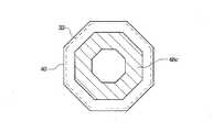
図1Bを参照する。図1Bは、UBMパッド4、アルミニウムパッド8、アルミニウム配線16、アルミニウムコンタクト18及びビア20a,20b,20cを示すレイアウト図である。外側の八角形領域はアルミニウムパッド8を表す。中間の八角形領域はUBMパッド4を表す。内側の八角形領域はUBMパッド4の凹部を表す。 Refer to FIG. 1B. FIG. 1B is a layout diagram showing the
図1A及び図1Bを参照する。図1A及び図1Bに示すように、バンプパッドは、一般にフリップチップアセンブリに応用する。フリップチップアセンブリは、そのスケーラビリティにより小型化の技術に適用することができるため、最新の科学技術に応用することができる。取り付けサイズの縮小に伴い(特に22nm技術において)、低誘電体の使用が普及し、特に、誘電率が2.5より低い場合、バンプパッドからの機械応力の衝撃力が増大する。そのため、例えば、半導体装置と付着するパッケージ基板との間の熱膨張係数(Coefficient of Thermal Expansion:CTE)のミスマッチにより発生する剥離又はせん断力により、バンプパッドが応力を受け、例えば、USG、低誘電体又は半田バンプが破裂するなどして半導体装置に故障が発生する虞がある。 Please refer to FIG. 1A and FIG. 1B. As shown in FIGS. 1A and 1B, bump pads generally apply to flip chip assemblies. The flip chip assembly can be applied to the technology of miniaturization due to its scalability, and thus can be applied to the latest science and technology. As the mounting size is reduced (especially in 22 nm technology), the use of low dielectrics is prevalent, especially when the dielectric constant is lower than 2.5, the impact force of mechanical stress from the bump pads increases. Therefore, for example, the bump pad receives stress due to peeling or shearing force generated due to a mismatch of thermal expansion coefficient (Coefficient of Thermal Expansion: CTE) between the semiconductor device and the attached package substrate. There is a risk that the semiconductor device may fail due to the body or solder bumps bursting.
フリップチップ技術でよく利用される他の構造としては、DBOC(Direct Bump On Copper)構造がある。UBMと最上メタライゼーション層の銅金属とは、DBOC構造中で直接接触される。無アルミニウムパッド(no aluminum pad)又はパッシベーション内層は、DBOC構造中に応用する。無アルミニウムパッド又はパッシベーション内層は、緩衝として用い、DBOC構造の機械強度が一般に低いため、上述したような問題が発生する虞がある。そのため、従来技術の問題点を解決するために、バンプパッドの機械強度を高めることが求められている。 Another structure often used in flip-chip technology is a DBOC (Direct Bump On Copper) structure. The UBM and the copper metal of the top metallization layer are in direct contact in the DBOC structure. An aluminum-free pad or inner passivation layer is applied in the DBOC structure. The aluminum-free pad or the inner passivation layer is used as a buffer, and the mechanical strength of the DBOC structure is generally low, so the above-described problems may occur. Therefore, in order to solve the problems of the prior art, it is required to increase the mechanical strength of the bump pad.
本発明は、バンプパッド構造の機械強度を高め、USG層と低誘電体層との間の界面を保護するバンプパッド構造及びその製造方法を提供することを目的とする。 An object of the present invention is to provide a bump pad structure that increases the mechanical strength of the bump pad structure and protects the interface between the USG layer and the low dielectric layer, and a method for manufacturing the same.
上記目的を達成するため、本発明の第1の観点に係るバンプパッド構造は、
USG層から形成された上層と低誘電率層から形成された下層とを有する基板と、
前記上層上に形成された強化パッドと、
前記上層の上方に形成された中間層と、
前記中間層上に形成された中間接続パッドと、
前記中間層の上方に形成された外層と、
前記外層に形成された開口を介し、前記中間接続パッドに接続されたUBMと、を備え、
前記強化パッドの半径又は外接円半径は、前記UBMの半径又は外接円半径より少なくとも5μm大きいことを特徴とする。In order to achieve the above object, the bump pad structure according to the first aspect of the present invention includes:
A substrate havingan upperlayer formed from a USG layerand a lower layer formed from a low dielectric constant layer ;
A reinforcing pad formed on the upper layer;
An intermediate layer formed above the upper layer;
An intermediate connection pad formed on the intermediate layer;
An outer layer formed above the intermediate layer;
A UBM connected to the intermediate connection pad through an opening formed in the outer layer,
The radius or circumscribed circle radius of the reinforcing pad is at least 5 μm larger than the radius or circumscribed circle radius of the UBM .
前記中間接続パッドと前記強化パッドとを物理的に接続するビアをさらに備えてもよい。 A via for physically connecting the intermediate connection pad and the reinforcing pad may be further provided.
前記ビアは、中空でないビア、環状のビア及び5×5のアレイ状に配列されたビアからなる群から選ばれるフィーチャを含んでもよい。 The vias may include features selected from the group consisting of non-hollow vias, annular vias and vias arranged in a 5 × 5 array.
前記中間接続パッドの厚さは2.5μmでもよい。 The thickness of the intermediate connection pad may be 2.5 μm.
前記下層上に形成された第2の強化パッドと、
前記強化パッドと前記第2の強化パッドとを物理的に接続する第2のビアと、をさらに備えてもよい。A second reinforcing pads formedbefore Symbollower layer,
A second via that physically connects the reinforcing pad and the second reinforcing pad may be further included.
上記目的を達成するために、本発明の第2の観点に係るバンプパッド構造の製造方法は、
USG層から形成された上層と低誘電率層から形成された下層とを有する基板の上層上に強化パッドを形成する工程と、
前記基板の前記上層上に中間層を形成する工程と、
前記中間層上に中間接続パッドを形成し、前記中間層のビアを介し、前記中間接続パッドと前記強化パッドとを接続させる工程と、
前記基板上に外層を形成する工程と、
前記外層の開口の中にUBMを形成し、前記UBMを前記中間接続パッドに接続させる工程と、を含み、
前記強化パッドの半径又は外接円半径は、前記UBMの半径又は外接円半径より少なくとも5μm大きいことを特徴とする。In order to achieve the above object, a method of manufacturing a bump pad structure according to the second aspect of the present invention includes:
Forming a reinforcing pad on an upper layerof a substratehaving an upper layer formed from a USG layer and a lower layer formed from a low dielectric constant layer ;
Forming an intermediate layer on the upper layer of the substrate;
Forming an intermediate connection pad on the intermediate layer, and connecting the intermediate connection pad and the reinforcing pad via a via in the intermediate layer;
Forming an outer layer on the substrate;
Forming a UBM into the opening of the outer layer,seen including a step of connecting the UBM to the intermediate connecting pads,and
The radius or circumscribed circle radius of the reinforcing pad is at least 5 μm larger than the radius or circumscribed circle radius of the UBM .
前記基板の前記下層上に第2の強化パッドを形成する工程をさらに含み、
前記強化パッドを形成する工程は、前記基板の前記上層に、前記強化パッドと前記第2の強化パッドとを接続させる第2のビアを形成する工程を含んでもよい。Forming a second reinforcing pad on thelower layer of the substrate;
The step of forming the reinforcing pad may include a step of forming a second via for connecting the reinforcing pad and the second reinforcing pad in the upper layer of the substrate.
前記強化パッドを形成する工程は、
前記基板の前記上層上に形成されたレジスト層をパターニングし、前記上層中の前記強化パッドを配置する領域を露出させる工程と、
前記上層の露出された領域をエッチングする工程と、
前記上層上に金属を堆積する工程と、を含んでもよい。The step of forming the reinforcing pad includes:
Patterning a resist layer formed on the upper layer of the substrate to expose a region in the upper layer where the reinforcing pad is disposed;
Etching the exposed region of the upper layer;
Depositing a metal on the upper layer.
前記中間接続パッドを形成する工程は、
前記中間層上の第1のレジスト層をパターニングし、前記中間層中の前記ビアが形成される領域を露出させる工程と、
前記中間層の露出された領域をエッチングする工程と、
前記中間層上に金属層を堆積し、メタライゼーション層及び前記ビアを形成する工程と、
前記メタライゼーション層上に形成されたレジスト層をパターニングし、前記メタライゼーション層により、前記中間接続パッドの一部が露出されないようにする工程と、
前記メタライゼーション層の露出部分をエッチングする工程と、を含んでもよい。The step of forming the intermediate connection pad includes:
Patterning a first resist layer on the intermediate layer to expose a region in the intermediate layer where the via is formed;
Etching the exposed region of the intermediate layer;
Depositing a metal layer on the intermediate layer to form a metallization layer and the via;
Patterning a resist layer formed on the metallization layer to prevent a portion of the intermediate connection pad from being exposed by the metallization layer;
Etching the exposed portion of the metallization layer.
前記UBMを形成する工程は、
前記外層の上方に形成されたレジスト層をパターニングし、前記外層の前記開口が形成される領域を露出させる工程と、
前記外層をエッチングし、前記開口を形成する工程と、を含んでもよい。The step of forming the UBM includes:
Patterning a resist layer formed above the outer layer to expose a region of the outer layer where the opening is formed;
Etching the outer layer to form the opening.
本発明のバンプパッド構造及びその製造方法は、バンプパッド構造の機械強度を高め、USG層と低誘電体層との間の界面を保護することができる。 The bump pad structure and the manufacturing method thereof of the present invention can increase the mechanical strength of the bump pad structure and protect the interface between the USG layer and the low dielectric layer.
(第1実施形態)
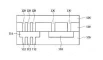
図2を参照する。図2は、本発明の第1実施形態に係るバンプパッド構造を示す断面図である。半田バンプ30は、半導体チップ上の外側のパッシベーション層34中に設けられた開口を介し、アルミニウムパッド36に接続されたUBMパッド32と物理的に接続されている。アルミニウムパッド36は、低誘電率の誘電体層44上のUSG層42の上方に設けられている内側のパッシベーション層38上に配置されている。中空でない銅パッド40は、USG層42上かつアルミニウムパッド36の下方に設けられている。低誘電率の誘電体層44は、回路46をさらに含んでもよい。これらの層は、その他よく知られた方式で配置したり、その他の材料を含んでもよい。例えば、低誘電率の誘電体層44がUSG層で代替されたり、相互接続構造がアルミニウム配線(図2、図3及び図8では図示せず)を介し、アルミニウムパッド36と電気的に接続されたりしてもよい。(First embodiment)
Please refer to FIG. FIG. 2 is a cross-sectional view showing a bump pad structure according to the first embodiment of the present invention. The
(第2実施形態)
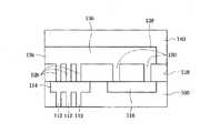
図3は、本発明の第2実施形態に係るバンプパッド構造を示す断面図である。図3の構造は、図2と同様に、数個のビア48を有する以外に、これらビア48を介してアルミニウムパッド36が銅パッド40に接続されている。(Second Embodiment)
FIG. 3 is a sectional view showing a bump pad structure according to the second embodiment of the present invention. In the structure of FIG. 3, the
上述の実施形態では、USG層42及び低誘電率の誘電体層44の応力を下げることができる。図4は、USG層42と低誘電率の誘電体層44との間の界面箇所に発生する応力が減少する状態を示すグラフである。図1Aは、従来のアルミニウムパッドを示す断面図である。図2は、銅パッドを有するアルミニウムパッドを示す断面図である。図3は、銅パッド及びビアコネクションを備えるアルミニウムパッドを示す断面図である。従来のパッドをベースラインとして用い、界面上の応力を正規化する。アルミニウムパッド及び銅パッド構造(図2に示す)は、剥離応力が正規化ベースラインで9%低下し、せん断力が正規化ベースラインで12%低下する。ビア構造を有するアルミニウムパッド及び銅パッド構造(図3に示す)は、剥離応力が正規化ベースラインで15%低下し、せん断力が正規化ベースラインで22%低下する。 In the above-described embodiment, the stress of the
界面上の応力は、銅パッド40により発生するヤング率の増大に伴い低下する。低誘電体のヤング率は約10GPaであり、USGのヤング率は約70GPaであるが、銅のヤング率は約218GPaである。そのため、銅が挿入された構造は、ヤング係数が向上して機械強度が高くなるため、界面を好適に保護することができる。 The stress on the interface decreases as the Young's modulus generated by the
このタイプの構造は、USG層42の応力に影響を与える上、銅パッド40のサイズもこの応力に影響を与える。図5は、銅パッド40のサイズが応力に与える影響を示すグラフである。図5のx軸は差Δを表し、その単位はマイクロメートルである。差Δとは、図3が示すUBMパッド32の外接円半径と、銅パッド40の外接円半径との差である。図5に示すように、ベースラインによりUSG層42と低誘電率の誘電体層44との間の界面上の応力を正規化する。このベースラインは、銅パッド40の外接円半径がUBMパッド32の外接円半径に等しいときの差Δがゼロである。図5のグラフから分かるように、応力は、差Δの増加に伴って減少するが、差Δが5μmを超えると、正規化応力の減少に伴い小さくなる。即ち、差Δは、5μmのときに飽和するといえる。差Δは、何れのサイズでもよいが、5μmであることが好ましい。 This type of structure affects the stress of the
さらに、アルミニウムパッド36を用いて銅パッド40のビア48に接続するレイアウトは、USG層42及び低誘電率の誘電体層44に与える応力に影響を与える。図6A〜図6Dは、数種類のビア48を示すレイアウト図である。図6Aは、中空でない八角形ビア48aを示すレイアウト図である。図6Aでは、UBMパッド32が点線により表され、銅パッド40が実線により表されている。UBMパッド32の外接円半径は、約75〜120μmである。アルミニウムパッド36(図示せず)の外接円半径は、UBMパッド32の外接円半径より約4μmより大きい。図6Bに示すように、八角形環状ビア48bは、外側の外接円半径が内側の外接円半径より10μm大きい。図6Cに示すように、八角形環状ビア48cは、外側の外接円半径が内側の外接円半径より20μm大きい。図6Bのビアの表面積は、アルミニウムパッド36の表面積の28.4%であり、図6Cのビアの表面積は、アルミニウムパッド36の表面積の52.1%である。また、八角形環状のビア48b及びビア48cの内側の外接円半径と外側の外接円半径との差は、例えば、5μm又は25μmに増減させてもよい。差が5μmである場合、ビアの表面積はアルミニウムパッド36の14.8%であり、差が25μmである場合、ビアの表面積はアルミニウムパッド36の62.1%である。図6Dは、5×5のアレイ状に配列されたビア48dを示すレイアウト図である。 Further, the layout using the
図7を参照する。図7は、USG層42と低誘電率の誘電体層44との界面にこれら異なるレイアウトが与える影響を示すグラフである。図6Aの中空でない八角形ビア48aをベースラインとして用い、その他全てのレイアウトは、このレイアウトに基づいて正規化を行う。図7のグラフから分かるように、正規化を行った後の応力は、ベースラインから図6C中の20μmの八角形環状ビア48cまで縮小し、図6D中の5×5のアレイ状に配列されたビア48dに縮小してから、図6B中の10μmの八角形環状ビア48bまで縮小する。 Please refer to FIG. FIG. 7 is a graph showing the influence of these different layouts on the interface between the
上述の実施形態の欠点は、USG層42中の銅パッド40がさらに大きな面積が必要となったり、USG層42に付加的な金属層が必要となったりする点である。本実施形態は、図1A中のバンプパッドと異なり、USG層42中の上金属層上に、銅パッド40を設けるために用いる領域が必要である。これにより、銅パッド40を設ける領域を得るために、上金属層上の回路システムの配線を改めて設定し直す必要がある。或いは、銅パッド40を設けるために、USG層42中へ付加的に金属層を設けてもよい。この場合、既存の半導体装置の回路システムの配線を改めて設計する必要はないが、付加的な金属層により工程が増えて材料にかかる費用が多くなる。 The drawback of the above-described embodiment is that the
(第3実施形態)
図8は、本発明の第3実施形態に係るバンプパッド構造を示す断面図である。図8は、図3の実施形態に類似するが、第2の銅パッド52がUSG層42の下方かつ低誘電率の誘電体層44上に位置する点が異なる。銅パッド40は、数個のビア50を介して第2の銅パッド52に接続されている。ビア50は、1つ又は多数の単独のビアでもよいし、図6A〜図6Dのレイアウトに対応したビアでもよい。さらに、より多くの銅パッドを図8の構造中に加えてもよい。これら銅パッドは、USG層42を含む多重金属層中に設けたり、USG層42及び低誘電率の誘電体層44中に設けたりしてもよい。多数の銅パッドは、ビアを利用して接続したりしなくてもよい。第2の銅パッド52を加えると、構造のヤング率が高まり、構造全体の機械強度が高まる。(Third embodiment)
FIG. 8 is a sectional view showing a bump pad structure according to the third embodiment of the present invention. FIG. 8 is similar to the embodiment of FIG. 3 except that the
本実施形態は、その他の特徴として、アルミニウムパッド36及び/又はアルミニウム配線が厚い点、USG層42が厚い点、又は下方の銅パッドを有さず、内側のパッシベーション層38に形成された数個のビア48だけを含む点がある。一般に、アルミニウムパッド36の厚さは約1.45μmである。この厚さは、例えば2.5μmまで増大させると、構造の機械強度が向上し、USG層42及び低誘電率の誘電体層44を保護することができる。同様に、USG層42の厚さを大きくすると、USG層42の機械強度が高まり、USG層42及び低誘電率の誘電体層44を保護することができる。USG層42の厚さを大きくする方式としては、USG層42の中にすでに存在する層を厚くする方式や、USG層42の中へ新たに数層を加える方式を利用してもよい。内側のパッシベーション層38に形成され、下方の銅パッドを備えていない数個のビア48の機械強度は、従来のバンプパッドより大きい。 In the present embodiment, as other features, the
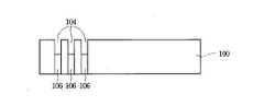
図9A〜図9Mを参照する。図9A〜図9Mは、本発明の一実施形態に係る、図3のバンプパッド構造の製造工程を行うときの状態を示す断面図である。図9Aに示すように、低誘電体層(図示せず)上にUSG層100を形成する。図9Bに示すように、USG層100上のフォトレジスト層102をパターニングし、数個の相互接続ビア開口104のエッチング箇所からUSG層100を露出させる。続いて、従来のフォトリソグラフィ技術を利用し、相互接続ビア開口104をエッチングする。次に、図9Cに示すように、相互接続ビア開口104の一部に、数個のプラグ(plug)106を充填してからフォトレジスト層102を除去する。図9Dに示すように、USG層100上にもう一つのフォトレジスト層108を形成してから、フォトレジスト層108をパターニングし、相互接続ビア開口104上の相互接続コンタクトが形成された箇所と、銅パッドが形成された箇所とから、USG層100が露出される。続いて、従来のフォトリソグラフィ技術を利用してUSG層100に対してエッチングを行い、少なくともプラグ106の頂部の位置までエッチングを行う。 Please refer to FIG. 9A to FIG. 9M. 9A to 9M are cross-sectional views illustrating states when performing the manufacturing process of the bump pad structure of FIG. 3 according to an embodiment of the present invention. As shown in FIG. 9A, a
図9Eに示すように、フォトレジスト層108及びプラグ106を除去する。続いて、USG層100上に銅110を堆積する。また、銅110を堆積する前に、物理気相堆積を利用し、拡散障壁層を形成してもよい。また、拡散障壁層を形成した後で、銅110を堆積する前に、電解メッキが都合良く行えるように、銅シード層(copper seed layer)を形成してもよい。図9Fに示すように、例えば、化学機械研磨を利用し、余分な銅110を除去し、数個の相互接続ビア112、相互接続コンタクト114及び銅パッド116を形成してもよい。或いは、従来のデュアルダマシン製造工程を利用し、相互接続ビア112、相互接続コンタクト114及び銅パッド116を形成してもよい。 As shown in FIG. 9E, the
図9Gに示すように、USG層100の上方に、第1のパッシベーション層118が堆積される。図9Hに示すように、第1のパッシベーション層118上に、フォトレジスト層120が形成される。フォトレジスト層120をパターニングすると、相互接続コンタクト114及び銅パッド116上に設けられた第1のパッシベーション層118の一部が露出される。続いて、従来のフォトリソグラフィ技術を利用して第1のパッシベーション層118をエッチングすると、数個のビア開口122,124が残存される。図9Iに示すように、フォトレジスト層120を除去し、アルミニウム126を堆積する。アルミニウム126は、第1のビア開口122に充填されてアルミニウム相互接続ビア128が形成され、第2のビア開口124を充填してアルミニウムビア130が形成される。図9Jに示すように、アルミニウム126の上方に形成したフォトレジスト層132をパターニングし、アルミニウム相互接続コンタクト134、アルミニウム配線136及びアルミニウムパッド138を形成する。続いて、アルミニウム126をエッチングしてパターニングし、素子が形成される。 As shown in FIG. 9G, a
図9Kに示すように、フォトレジスト層132を除去した後、この構造上に第2のパッシベーション層140を堆積させる。図9Lに示すように、第2のパッシベーション層140上にフォトレジスト層142を形成する。そして、このフォトレジスト層142をパターニングし、アルミニウムパッド138上に形成された第2のパッシベーション層140の一部を露出させる。続いて、第2のパッシベーション層140をアルミニウムパッド138の位置までエッチングし、UBM開口144を残存させる。図9Mに示すように、フォトレジスト層142を除去した後、UBM開口144中にUBMパッド146を形成し、UBMパッド146とアルミニウムパッド138とを接続させる。 As shown in FIG. 9K, after removing the
当該分野の技術を熟知するものが理解できるように、本発明の好適な実施形態を前述の通り開示したが、これらは決して本発明を限定するものではない。本発明の主旨と範囲を逸脱しない範囲内で各種の変更や修正を加えることができる。従って、本発明による特許請求の範囲は、このような変更や修正を含めて広く解釈されるべきである。例えば、上述の実施形態の多くの特徴には、銅又はアルミニウムが含まれているが、アルミニウムの代わりに銅を用いたり、銅の代わりにアルミニウムを用いたりしてもよい。当業者であれば容易に分かるように、上述した各層(例えば、パッシベーション層、USG層、誘電体層など)は何ら限定されるわけではなく、その他の層を用いてもよい。While the preferred embodiments of the present invention have been disclosed above, as may be appreciated by those skilled in the art, they are not intended to limit the invention in any way. Various changes and modifications can be made without departing from the spirit and scope of the present invention. Accordingly, the scope of the claims according to the present invention should be construed broadly including such changes and modifications. For example, many features of the above-described embodiments include copper or aluminum, but copper may be used instead of aluminum, or aluminum may be used instead of copper. As will be readily understood by those skilled in the art, the above-described layers (for example, a passivation layer, a USG layer, a dielectric layer, etc.) are not limited at all, and other layers may be used.
2 半田バンプ
4 UBMパッド
6 外側のパッシベーション層
8 アルミニウムパッド
10 内側のパッシベーション層
12 USG層
14 低誘電率の誘電体層
16 アルミニウム配線
18 アルミニウムコンタクト
20a ビア
20b ビア
20c ビア
22 第1のコンタクト
24 ビア
26 第2のコンタクト
30 半田バンプ
32 UBMパッド
34 外側のパッシベーション層
36 アルミニウムパッド
38 内側のパッシベーション層
40 銅パッド
42 USG層
44 低誘電率の誘電体層
46 回路
48 ビア
48a ビア
48b ビア
48c ビア
48d ビア
50 ビア
52 銅パッド
100 USG層
102 フォトレジスト層
104 相互接続ビア開口
106 プラグ
108 フォトレジスト層
110 銅
112 相互接続ビア
114 相互接続コンタクト
116 銅パッド
118 第1のパッシベーション層
120 フォトレジスト層
122 第1のビア開口
124 第2のビア開口
126 アルミニウム
128 アルミニウム相互接続ビア
130 アルミニウムビア
132 フォトレジスト層
134 アルミニウム相互接続コンタクト
136 アルミニウム配線
138 アルミニウムパッド
140 第2のパッシベーション層
142 フォトレジスト層
144 UBM開口
146 UBMパッド2
Claims (10)
Translated fromJapanese前記上層上に形成された強化パッドと、
前記上層の上方に形成された中間層と、
前記中間層上に形成された中間接続パッドと、
前記中間層の上方に形成された外層と、
前記外層に形成された開口を介し、前記中間接続パッドに接続されたUBMと、を備え、
前記強化パッドの半径又は外接円半径は、前記UBMの半径又は外接円半径より少なくとも5μm大きいことを特徴とするバンプパッド構造。A substrate havingan upperlayer formed from a USG layerand a lower layer formed from a low dielectric constant layer ;
A reinforcing pad formed on the upper layer;
An intermediate layer formed above the upper layer;
An intermediate connection pad formed on the intermediate layer;
An outer layer formed above the intermediate layer;
A UBM connected to the intermediate connection pad through an opening formed in the outer layer,
The bump pad structure according toclaim 1, wherein the radius or circumscribed circle radius of the reinforcing pad is at least 5 μm larger than the radius or circumscribed circle radius of the UBM .
前記強化パッドと前記第2の強化パッドとを物理的に接続する第2のビアと、をさらに備えることを特徴とする請求項1に記載のバンプパッド構造。A second reinforcing pads formedbefore Symbollower layer,
The bump pad structure according to claim 1, further comprising a second via that physically connects the reinforcing pad and the second reinforcing pad.
前記基板の前記上層上に中間層を形成する工程と、
前記中間層上に中間接続パッドを形成し、前記中間層のビアを介し、前記中間接続パッドと前記強化パッドとを接続させる工程と、
前記基板上に外層を形成する工程と、
前記外層の開口の中にUBMを形成し、前記UBMを前記中間接続パッドに接続させる工程と、を含み、
前記強化パッドの半径又は外接円半径は、前記UBMの半径又は外接円半径より少なくとも5μm大きいことを特徴とするバンプパッド構造の製造方法。Forming a reinforcing pad on an upper layerof a substratehaving an upper layer formed from a USG layer and a lower layer formed from a low dielectric constant layer ;
Forming an intermediate layer on the upper layer of the substrate;
Forming an intermediate connection pad on the intermediate layer, and connecting the intermediate connection pad and the reinforcing pad via a via in the intermediate layer;
Forming an outer layer on the substrate;
Forming a UBM into the opening of the outer layer,seen including a step of connecting the UBM to the intermediate connecting pads,and
The bump pad structure manufacturing method according toclaim 1, wherein the radius or circumscribed circle radius of the reinforcing pad is at least 5 μm larger than the radius or circumscribed circle radius of the UBM .
前記強化パッドを形成する工程は、前記基板の前記上層に、前記強化パッドと前記第2の強化パッドとを接続させる第2のビアを形成する工程を含むことを特徴とする請求項6に記載のバンプパッド構造の製造方法。Forming a second reinforcing pad on thelower layer of the substrate;
The step of forming the reinforcing pad, the upper layer of the substrate, according to claim6, characterized in that it comprises a step of forming a second via for connecting the said reinforcement pad second reinforcement pad Bump pad structure manufacturing method.
前記基板の前記上層上に形成されたレジスト層をパターニングし、前記上層中の前記強化パッドを配置する領域を露出させる工程と、
前記上層の露出された領域をエッチングする工程と、
前記上層上に金属を堆積する工程と、を含むことを特徴とする請求項6に記載のバンプパッド構造の製造方法。The step of forming the reinforcing pad includes:
Patterning a resist layer formed on the upper layer of the substrate to expose a region in the upper layer where the reinforcing pad is disposed;
Etching the exposed region of the upper layer;
The method of manufacturing a bump pad structure according to claim6 , further comprising: depositing a metal on the upper layer.
前記中間層上の第1のレジスト層をパターニングし、前記中間層中の前記ビアが形成される領域を露出させる工程と、
前記中間層の露出された領域をエッチングする工程と、
前記中間層上に金属層を堆積し、メタライゼーション層及び前記ビアを形成する工程と、
前記メタライゼーション層上に形成されたレジスト層をパターニングし、前記メタライゼーション層により、前記中間接続パッドの一部が露出されないようにする工程と、
前記メタライゼーション層の露出部分をエッチングする工程と、を含むことを特徴とする請求項6に記載のバンプパッド構造の製造方法。The step of forming the intermediate connection pad includes:
Patterning a first resist layer on the intermediate layer to expose a region in the intermediate layer where the via is formed;
Etching the exposed region of the intermediate layer;
Depositing a metal layer on the intermediate layer to form a metallization layer and the via;
Patterning a resist layer formed on the metallization layer to prevent a portion of the intermediate connection pad from being exposed by the metallization layer;
The method of manufacturing a bump pad structure according to claim6 , further comprising: etching an exposed portion of the metallization layer.
前記外層の上方に形成されたレジスト層をパターニングし、前記外層の前記開口が形成される領域を露出させる工程と、
前記外層をエッチングし、前記開口を形成する工程と、を含むことを特徴とする請求項6に記載のバンプパッド構造の製造方法。The step of forming the UBM includes:
Patterning a resist layer formed above the outer layer to expose a region of the outer layer where the opening is formed;
The method of manufacturing a bump pad structure according to claim6 , further comprising: etching the outer layer to form the opening.
Applications Claiming Priority (4)
| Application Number | Priority Date | Filing Date | Title |
|---|---|---|---|
| US17652209P | 2009-05-08 | 2009-05-08 | |
| US61/176,522 | 2009-05-08 | ||
| US12/726,449US8405211B2 (en) | 2009-05-08 | 2010-03-18 | Bump pad structure |
| US12/726,449 | 2010-03-18 |
Publications (2)
| Publication Number | Publication Date |
|---|---|
| JP2010263219A JP2010263219A (en) | 2010-11-18 |
| JP5143860B2true JP5143860B2 (en) | 2013-02-13 |
Family
ID=43061866
Family Applications (1)
| Application Number | Title | Priority Date | Filing Date |
|---|---|---|---|
| JP2010107035AActiveJP5143860B2 (en) | 2009-05-08 | 2010-05-07 | Bump pad structure and manufacturing method thereof |
Country Status (4)
| Country | Link |
|---|---|
| US (4) | US8405211B2 (en) |
| JP (1) | JP5143860B2 (en) |
| KR (1) | KR101178299B1 (en) |
| TW (1) | TWI451545B (en) |
Families Citing this family (27)
| Publication number | Priority date | Publication date | Assignee | Title |
|---|---|---|---|---|
| US8405211B2 (en)* | 2009-05-08 | 2013-03-26 | Taiwan Semiconductor Manufacturing Company, Ltd. | Bump pad structure |
| US9543262B1 (en)* | 2009-08-18 | 2017-01-10 | Cypress Semiconductor Corporation | Self aligned bump passivation |
| US9105588B2 (en)* | 2010-10-21 | 2015-08-11 | Taiwan Semiconductor Manufacturing Company, Ltd. | Semiconductor component having a second passivation layer having a first opening exposing a bond pad and a plurality of second openings exposing a top surface of an underlying first passivation layer |
| US8624392B2 (en) | 2011-06-03 | 2014-01-07 | Taiwan Semiconductor Manufacturing Company, Ltd. | Electrical connection for chip scale packaging |
| US9548281B2 (en)* | 2011-10-07 | 2017-01-17 | Taiwan Semiconductor Manufacturing Company, Ltd. | Electrical connection for chip scale packaging |
| US8912668B2 (en) | 2012-03-01 | 2014-12-16 | Taiwan Semiconductor Manufacturing Company, Ltd. | Electrical connections for chip scale packaging |
| KR101916088B1 (en) | 2012-04-02 | 2018-11-07 | 삼성전자주식회사 | Semiconductor Package |
| US9196573B2 (en) | 2012-07-31 | 2015-11-24 | Taiwan Semiconductor Manufacturing Company, Ltd. | Bump on pad (BOP) bonding structure |
| US8829673B2 (en) | 2012-08-17 | 2014-09-09 | Taiwan Semiconductor Manufacturing Company, Ltd. | Bonded structures for package and substrate |
| US9673161B2 (en) | 2012-08-17 | 2017-06-06 | Taiwan Semiconductor Manufacturing Company, Ltd. | Bonded structures for package and substrate |
| US8952530B2 (en)* | 2012-09-14 | 2015-02-10 | Taiwan Semiconductor Manufacturing Company, Ltd. | Post passivation interconnect structures and methods for forming the same |
| US9275925B2 (en)* | 2013-03-12 | 2016-03-01 | Taiwan Semiconductor Manufacturing Company, Ltd. | System and method for an improved interconnect structure |
| JP2015095482A (en) | 2013-11-08 | 2015-05-18 | アイメックImec | Method for producing microbumps on semiconductor component |
| TWI550801B (en)* | 2013-11-13 | 2016-09-21 | 南茂科技股份有限公司 | Package structure and manufacturing method thereof |
| CN105047643A (en)* | 2014-04-28 | 2015-11-11 | 联咏科技股份有限公司 | Integrated circuit with a plurality of transistors |
| US9899238B2 (en)* | 2014-12-18 | 2018-02-20 | Intel Corporation | Low cost package warpage solution |
| US10068181B1 (en)* | 2015-04-27 | 2018-09-04 | Rigetti & Co, Inc. | Microwave integrated quantum circuits with cap wafer and methods for making the same |
| US9711478B2 (en)* | 2015-10-19 | 2017-07-18 | Taiwan Semiconductor Manufacturing Company Ltd. | Semiconductor device with an anti-pad peeling structure and associated method |
| US10522485B2 (en)* | 2015-12-21 | 2019-12-31 | Intel IP Corporation | Electrical device and a method for forming an electrical device |
| US9842810B1 (en)* | 2016-06-08 | 2017-12-12 | Globalfoundries Inc. | Tiled-stress-alleviating pad structure |
| US9812414B1 (en) | 2016-06-17 | 2017-11-07 | Nanya Technology Corporation | Chip package and a manufacturing method thereof |
| US10256179B2 (en)* | 2017-02-06 | 2019-04-09 | Nanya Technology Corporation | Package structure and manufacturing method thereof |
| US11121301B1 (en) | 2017-06-19 | 2021-09-14 | Rigetti & Co, Inc. | Microwave integrated quantum circuits with cap wafers and their methods of manufacture |
| US10566300B2 (en)* | 2018-01-22 | 2020-02-18 | Globalfoundries Inc. | Bond pads with surrounding fill lines |
| US11417619B2 (en)* | 2019-08-22 | 2022-08-16 | Taiwan Semiconductor Manufacturing Company Ltd. | Package and manufacturing method thereof |
| KR102851594B1 (en)* | 2020-02-14 | 2025-08-28 | 삼성전자주식회사 | Semiconductor package and method of manufacturing the same |
| US11682641B2 (en)* | 2020-08-13 | 2023-06-20 | Microchip Technology Incorporated | Integrated circuit bond pad with multi-material toothed structure |
Family Cites Families (11)
| Publication number | Priority date | Publication date | Assignee | Title |
|---|---|---|---|---|
| JP2916326B2 (en)* | 1992-06-11 | 1999-07-05 | 三菱電機株式会社 | Pad structure of semiconductor device |
| JP2697592B2 (en)* | 1993-12-03 | 1998-01-14 | 日本電気株式会社 | Pad structure of semiconductor device |
| JP2002319587A (en)* | 2001-04-23 | 2002-10-31 | Seiko Instruments Inc | Semiconductor device |
| US20030020163A1 (en)* | 2001-07-25 | 2003-01-30 | Cheng-Yu Hung | Bonding pad structure for copper/low-k dielectric material BEOL process |
| US7741714B2 (en)* | 2004-11-02 | 2010-06-22 | Taiwan Semiconductor Manufacturing Co., Ltd. | Bond pad structure with stress-buffering layer capping interconnection metal layer |
| US7196428B2 (en)* | 2005-02-15 | 2007-03-27 | Taiwan Semiconductor Manufacturing Company, Ltd. | Bond pad structure for integrated circuit chip |
| WO2006091856A1 (en)* | 2005-02-24 | 2006-08-31 | Agere Systems Inc. | Structure and method for fabricating flip chip devices |
| US7622309B2 (en)* | 2005-06-28 | 2009-11-24 | Freescale Semiconductor, Inc. | Mechanical integrity evaluation of low-k devices with bump shear |
| US7364998B2 (en)* | 2005-07-21 | 2008-04-29 | Taiwan Semiconductor Manufacturing Co., Ltd. | Method for forming high reliability bump structure |
| US8319343B2 (en)* | 2005-09-21 | 2012-11-27 | Agere Systems Llc | Routing under bond pad for the replacement of an interconnect layer |
| US8405211B2 (en)* | 2009-05-08 | 2013-03-26 | Taiwan Semiconductor Manufacturing Company, Ltd. | Bump pad structure |
- 2010
- 2010-03-18USUS12/726,449patent/US8405211B2/enactiveActive
- 2010-05-05TWTW099114442Apatent/TWI451545B/enactive
- 2010-05-07JPJP2010107035Apatent/JP5143860B2/enactiveActive
- 2010-05-10KRKR1020100043610Apatent/KR101178299B1/enactiveActive
- 2013
- 2013-03-05USUS13/786,045patent/US8907478B2/enactiveActive
- 2014
- 2014-10-13USUS14/512,895patent/US9171811B2/enactiveActive
- 2015
- 2015-10-15USUS14/884,438patent/US9536847B2/enactiveActive
Also Published As
| Publication number | Publication date |
|---|---|
| US20150031200A1 (en) | 2015-01-29 |
| KR20100121447A (en) | 2010-11-17 |
| US8405211B2 (en) | 2013-03-26 |
| US9171811B2 (en) | 2015-10-27 |
| US9536847B2 (en) | 2017-01-03 |
| TW201041108A (en) | 2010-11-16 |
| JP2010263219A (en) | 2010-11-18 |
| US20100283148A1 (en) | 2010-11-11 |
| US20130181347A1 (en) | 2013-07-18 |
| US20160035684A1 (en) | 2016-02-04 |
| KR101178299B1 (en) | 2012-08-29 |
| US8907478B2 (en) | 2014-12-09 |
| TWI451545B (en) | 2014-09-01 |
Similar Documents
| Publication | Publication Date | Title |
|---|---|---|
| JP5143860B2 (en) | Bump pad structure and manufacturing method thereof | |
| JP5409993B2 (en) | Under bond pad path for interconnect layer replacement | |
| CN102222647B (en) | Semiconductor die and method of forming conductive elements | |
| US8492892B2 (en) | Solder bump connections | |
| US8456008B2 (en) | Structure and process for the formation of TSVs | |
| KR102410018B1 (en) | Semiconductor package | |
| US9312230B2 (en) | Conductive pillar structure for semiconductor substrate and method of manufacture | |
| JP5512082B2 (en) | Semiconductor device manufacturing method and semiconductor device | |
| US20080303154A1 (en) | Through-silicon via interconnection formed with a cap layer | |
| US20070087544A1 (en) | Method for forming improved bump structure | |
| CN104904006A (en) | Semiconductor device and its manufacturing method | |
| TW201203482A (en) | Conductive pillar for semiconductor substrate and method of manufacture | |
| US8399348B2 (en) | Semiconductor device for improving electrical and mechanical connectivity of conductive pillers and method therefor | |
| US8722529B2 (en) | Double solid metal pad with reduced area | |
| JP2020074436A (en) | Collars for under-bump metal structures and associated systems and methods | |
| US8115317B2 (en) | Semiconductor device including electrode structure with first and second openings and manufacturing method thereof | |
| JP2003152014A (en) | Semiconductor device and method for manufacturing the same | |
| JP2009124042A (en) | Semiconductor device | |
| JP5258142B2 (en) | Aluminum pad power bus and signal routing technology for integrated circuit devices using copper technology interconnect structures | |
| US7112522B1 (en) | Method to increase bump height and achieve robust bump structure | |
| TWI765853B (en) | Semiconductor device and manufacturing method thereof | |
| CN100423246C (en) | Bond pads containing tungsten or tungsten compounds on top of the metal layer | |
| JP4812673B2 (en) | Semiconductor device | |
| US20240047397A1 (en) | Bump structure and method of making the same | |
| JP2000332116A (en) | Semiconductor integrated circuit device and method of manufacturing the same |
Legal Events
| Date | Code | Title | Description |
|---|---|---|---|
| RD04 | Notification of resignation of power of attorney | Free format text:JAPANESE INTERMEDIATE CODE: A7424 Effective date:20111115 | |
| A977 | Report on retrieval | Free format text:JAPANESE INTERMEDIATE CODE: A971007 Effective date:20120131 | |
| A131 | Notification of reasons for refusal | Free format text:JAPANESE INTERMEDIATE CODE: A131 Effective date:20120207 | |
| A521 | Request for written amendment filed | Free format text:JAPANESE INTERMEDIATE CODE: A523 Effective date:20120502 | |
| TRDD | Decision of grant or rejection written | ||
| A01 | Written decision to grant a patent or to grant a registration (utility model) | Free format text:JAPANESE INTERMEDIATE CODE: A01 Effective date:20121113 | |
| A01 | Written decision to grant a patent or to grant a registration (utility model) | Free format text:JAPANESE INTERMEDIATE CODE: A01 | |
| A61 | First payment of annual fees (during grant procedure) | Free format text:JAPANESE INTERMEDIATE CODE: A61 Effective date:20121121 | |
| FPAY | Renewal fee payment (event date is renewal date of database) | Free format text:PAYMENT UNTIL: 20151130 Year of fee payment:3 | |
| R150 | Certificate of patent or registration of utility model | Ref document number:5143860 Country of ref document:JP Free format text:JAPANESE INTERMEDIATE CODE: R150 Free format text:JAPANESE INTERMEDIATE CODE: R150 | |
| R250 | Receipt of annual fees | Free format text:JAPANESE INTERMEDIATE CODE: R250 | |
| R250 | Receipt of annual fees | Free format text:JAPANESE INTERMEDIATE CODE: R250 | |
| R250 | Receipt of annual fees | Free format text:JAPANESE INTERMEDIATE CODE: R250 | |
| R250 | Receipt of annual fees | Free format text:JAPANESE INTERMEDIATE CODE: R250 | |
| R250 | Receipt of annual fees | Free format text:JAPANESE INTERMEDIATE CODE: R250 | |
| R250 | Receipt of annual fees | Free format text:JAPANESE INTERMEDIATE CODE: R250 | |
| R250 | Receipt of annual fees | Free format text:JAPANESE INTERMEDIATE CODE: R250 | |
| R250 | Receipt of annual fees | Free format text:JAPANESE INTERMEDIATE CODE: R250 | |
| R250 | Receipt of annual fees | Free format text:JAPANESE INTERMEDIATE CODE: R250 | |
| R250 | Receipt of annual fees | Free format text:JAPANESE INTERMEDIATE CODE: R250 |