JP5141541B2 - Epitaxial wafer manufacturing method - Google Patents
Epitaxial wafer manufacturing methodDownload PDFInfo
- Publication number
- JP5141541B2 JP5141541B2JP2008327274AJP2008327274AJP5141541B2JP 5141541 B2JP5141541 B2JP 5141541B2JP 2008327274 AJP2008327274 AJP 2008327274AJP 2008327274 AJP2008327274 AJP 2008327274AJP 5141541 B2JP5141541 B2JP 5141541B2
- Authority
- JP
- Japan
- Prior art keywords
- semiconductor wafer
- wafer
- oxide film
- back surface
- epitaxial
- Prior art date
- Legal status (The legal status is an assumption and is not a legal conclusion. Google has not performed a legal analysis and makes no representation as to the accuracy of the status listed.)
- Active
Links
- 238000004519manufacturing processMethods0.000titleclaimsdescription29
- 239000004065semiconductorSubstances0.000claimsdescription215
- 230000002093peripheral effectEffects0.000claimsdescription37
- 238000000034methodMethods0.000claimsdescription32
- 238000005530etchingMethods0.000claimsdescription30
- 230000008569processEffects0.000claimsdescription23
- 230000002209hydrophobic effectEffects0.000claimsdescription17
- 238000001947vapour-phase growthMethods0.000claimsdescription12
- 238000009434installationMethods0.000claimsdescription8
- 235000012431wafersNutrition0.000description332
- XUIMIQQOPSSXEZ-UHFFFAOYSA-NSiliconChemical compound[Si]XUIMIQQOPSSXEZ-UHFFFAOYSA-N0.000description32
- 229910052710siliconInorganic materials0.000description32
- 239000010703siliconSubstances0.000description32
- 238000006243chemical reactionMethods0.000description22
- 239000012495reaction gasSubstances0.000description20
- 239000000243solutionSubstances0.000description15
- KRHYYFGTRYWZRS-UHFFFAOYSA-NFluoraneChemical groupFKRHYYFGTRYWZRS-UHFFFAOYSA-N0.000description14
- XLYOFNOQVPJJNP-UHFFFAOYSA-NwaterSubstancesOXLYOFNOQVPJJNP-UHFFFAOYSA-N0.000description13
- 238000004140cleaningMethods0.000description10
- 239000007788liquidSubstances0.000description10
- 238000010438heat treatmentMethods0.000description8
- 239000000126substanceSubstances0.000description7
- 239000007864aqueous solutionSubstances0.000description6
- VYPSYNLAJGMNEJ-UHFFFAOYSA-NSilicium dioxideChemical compoundO=[Si]=OVYPSYNLAJGMNEJ-UHFFFAOYSA-N0.000description5
- 230000007423decreaseEffects0.000description5
- 238000010586diagramMethods0.000description5
- CBENFWSGALASAD-UHFFFAOYSA-NOzoneChemical compound[O-][O+]=OCBENFWSGALASAD-UHFFFAOYSA-N0.000description4
- 230000015572biosynthetic processEffects0.000description4
- 239000007789gasSubstances0.000description4
- 238000012545processingMethods0.000description4
- UFHFLCQGNIYNRP-UHFFFAOYSA-NHydrogenChemical compound[H][H]UFHFLCQGNIYNRP-UHFFFAOYSA-N0.000description3
- 229910004298SiO 2Inorganic materials0.000description3
- SLLGVCUQYRMELA-UHFFFAOYSA-NchlorosiliconChemical compoundCl[Si]SLLGVCUQYRMELA-UHFFFAOYSA-N0.000description3
- 239000002019doping agentSubstances0.000description3
- 239000000463materialSubstances0.000description3
- 238000002156mixingMethods0.000description3
- 230000001590oxidative effectEffects0.000description3
- 229910052814silicon oxideInorganic materials0.000description3
- 239000007921spraySubstances0.000description3
- 230000009471actionEffects0.000description2
- 230000000052comparative effectEffects0.000description2
- 238000013461designMethods0.000description2
- 238000009826distributionMethods0.000description2
- QPJSUIGXIBEQAC-UHFFFAOYSA-Nn-(2,4-dichloro-5-propan-2-yloxyphenyl)acetamideChemical compoundCC(C)OC1=CC(NC(C)=O)=C(Cl)C=C1ClQPJSUIGXIBEQAC-UHFFFAOYSA-N0.000description2
- 239000010453quartzSubstances0.000description2
- OKTJSMMVPCPJKN-UHFFFAOYSA-NCarbonChemical compound[C]OKTJSMMVPCPJKN-UHFFFAOYSA-N0.000description1
- 230000008901benefitEffects0.000description1
- 229910052799carbonInorganic materials0.000description1
- 239000013078crystalSubstances0.000description1
- 230000006866deteriorationEffects0.000description1
- 238000007865dilutingMethods0.000description1
- 230000000694effectsEffects0.000description1
- 229910052736halogenInorganic materials0.000description1
- 150000002367halogensChemical class0.000description1
- 230000006698inductionEffects0.000description1
- 230000010354integrationEffects0.000description1
- 230000007246mechanismEffects0.000description1
- 239000008155medical solutionSubstances0.000description1
- 230000028161membrane depolarizationEffects0.000description1
- 239000011259mixed solutionSubstances0.000description1
- 239000000203mixtureSubstances0.000description1
- 238000012986modificationMethods0.000description1
- 230000004048modificationEffects0.000description1
- 238000000206photolithographyMethods0.000description1
- 229910021420polycrystalline siliconInorganic materials0.000description1
- 230000002265preventionEffects0.000description1
- 230000009467reductionEffects0.000description1
- 230000007480spreadingEffects0.000description1
- 238000003892spreadingMethods0.000description1
- 238000012360testing methodMethods0.000description1
- 238000005979thermal decomposition reactionMethods0.000description1
Images


Classifications
- H—ELECTRICITY
- H01—ELECTRIC ELEMENTS
- H01L—SEMICONDUCTOR DEVICES NOT COVERED BY CLASS H10
- H01L21/00—Processes or apparatus adapted for the manufacture or treatment of semiconductor or solid state devices or of parts thereof
- H01L21/67—Apparatus specially adapted for handling semiconductor or electric solid state devices during manufacture or treatment thereof; Apparatus specially adapted for handling wafers during manufacture or treatment of semiconductor or electric solid state devices or components ; Apparatus not specifically provided for elsewhere
- H01L21/683—Apparatus specially adapted for handling semiconductor or electric solid state devices during manufacture or treatment thereof; Apparatus specially adapted for handling wafers during manufacture or treatment of semiconductor or electric solid state devices or components ; Apparatus not specifically provided for elsewhere for supporting or gripping
- H01L21/687—Apparatus specially adapted for handling semiconductor or electric solid state devices during manufacture or treatment thereof; Apparatus specially adapted for handling wafers during manufacture or treatment of semiconductor or electric solid state devices or components ; Apparatus not specifically provided for elsewhere for supporting or gripping using mechanical means, e.g. chucks, clamps or pinches
- H01L21/68714—Apparatus specially adapted for handling semiconductor or electric solid state devices during manufacture or treatment thereof; Apparatus specially adapted for handling wafers during manufacture or treatment of semiconductor or electric solid state devices or components ; Apparatus not specifically provided for elsewhere for supporting or gripping using mechanical means, e.g. chucks, clamps or pinches the wafers being placed on a susceptor, stage or support
- H01L21/68742—Apparatus specially adapted for handling semiconductor or electric solid state devices during manufacture or treatment thereof; Apparatus specially adapted for handling wafers during manufacture or treatment of semiconductor or electric solid state devices or components ; Apparatus not specifically provided for elsewhere for supporting or gripping using mechanical means, e.g. chucks, clamps or pinches the wafers being placed on a susceptor, stage or support characterised by a lifting arrangement, e.g. lift pins
- C—CHEMISTRY; METALLURGY
- C23—COATING METALLIC MATERIAL; COATING MATERIAL WITH METALLIC MATERIAL; CHEMICAL SURFACE TREATMENT; DIFFUSION TREATMENT OF METALLIC MATERIAL; COATING BY VACUUM EVAPORATION, BY SPUTTERING, BY ION IMPLANTATION OR BY CHEMICAL VAPOUR DEPOSITION, IN GENERAL; INHIBITING CORROSION OF METALLIC MATERIAL OR INCRUSTATION IN GENERAL
- C23C—COATING METALLIC MATERIAL; COATING MATERIAL WITH METALLIC MATERIAL; SURFACE TREATMENT OF METALLIC MATERIAL BY DIFFUSION INTO THE SURFACE, BY CHEMICAL CONVERSION OR SUBSTITUTION; COATING BY VACUUM EVAPORATION, BY SPUTTERING, BY ION IMPLANTATION OR BY CHEMICAL VAPOUR DEPOSITION, IN GENERAL
- C23C16/00—Chemical coating by decomposition of gaseous compounds, without leaving reaction products of surface material in the coating, i.e. chemical vapour deposition [CVD] processes
- C23C16/44—Chemical coating by decomposition of gaseous compounds, without leaving reaction products of surface material in the coating, i.e. chemical vapour deposition [CVD] processes characterised by the method of coating
- C23C16/4411—Cooling of the reaction chamber walls
- C—CHEMISTRY; METALLURGY
- C23—COATING METALLIC MATERIAL; COATING MATERIAL WITH METALLIC MATERIAL; CHEMICAL SURFACE TREATMENT; DIFFUSION TREATMENT OF METALLIC MATERIAL; COATING BY VACUUM EVAPORATION, BY SPUTTERING, BY ION IMPLANTATION OR BY CHEMICAL VAPOUR DEPOSITION, IN GENERAL; INHIBITING CORROSION OF METALLIC MATERIAL OR INCRUSTATION IN GENERAL
- C23C—COATING METALLIC MATERIAL; COATING MATERIAL WITH METALLIC MATERIAL; SURFACE TREATMENT OF METALLIC MATERIAL BY DIFFUSION INTO THE SURFACE, BY CHEMICAL CONVERSION OR SUBSTITUTION; COATING BY VACUUM EVAPORATION, BY SPUTTERING, BY ION IMPLANTATION OR BY CHEMICAL VAPOUR DEPOSITION, IN GENERAL
- C23C16/00—Chemical coating by decomposition of gaseous compounds, without leaving reaction products of surface material in the coating, i.e. chemical vapour deposition [CVD] processes
- C23C16/44—Chemical coating by decomposition of gaseous compounds, without leaving reaction products of surface material in the coating, i.e. chemical vapour deposition [CVD] processes characterised by the method of coating
- C23C16/48—Chemical coating by decomposition of gaseous compounds, without leaving reaction products of surface material in the coating, i.e. chemical vapour deposition [CVD] processes characterised by the method of coating by irradiation, e.g. photolysis, radiolysis, particle radiation
- C23C16/481—Chemical coating by decomposition of gaseous compounds, without leaving reaction products of surface material in the coating, i.e. chemical vapour deposition [CVD] processes characterised by the method of coating by irradiation, e.g. photolysis, radiolysis, particle radiation by radiant heating of the substrate
- C—CHEMISTRY; METALLURGY
- C23—COATING METALLIC MATERIAL; COATING MATERIAL WITH METALLIC MATERIAL; CHEMICAL SURFACE TREATMENT; DIFFUSION TREATMENT OF METALLIC MATERIAL; COATING BY VACUUM EVAPORATION, BY SPUTTERING, BY ION IMPLANTATION OR BY CHEMICAL VAPOUR DEPOSITION, IN GENERAL; INHIBITING CORROSION OF METALLIC MATERIAL OR INCRUSTATION IN GENERAL
- C23C—COATING METALLIC MATERIAL; COATING MATERIAL WITH METALLIC MATERIAL; SURFACE TREATMENT OF METALLIC MATERIAL BY DIFFUSION INTO THE SURFACE, BY CHEMICAL CONVERSION OR SUBSTITUTION; COATING BY VACUUM EVAPORATION, BY SPUTTERING, BY ION IMPLANTATION OR BY CHEMICAL VAPOUR DEPOSITION, IN GENERAL
- C23C24/00—Coating starting from inorganic powder
- C23C24/08—Coating starting from inorganic powder by application of heat or pressure and heat
- C23C24/082—Coating starting from inorganic powder by application of heat or pressure and heat without intermediate formation of a liquid in the layer
- H—ELECTRICITY
- H01—ELECTRIC ELEMENTS
- H01L—SEMICONDUCTOR DEVICES NOT COVERED BY CLASS H10
- H01L21/00—Processes or apparatus adapted for the manufacture or treatment of semiconductor or solid state devices or of parts thereof
- H01L21/02—Manufacture or treatment of semiconductor devices or of parts thereof
- H01L21/02104—Forming layers
- H01L21/02365—Forming inorganic semiconducting materials on a substrate
- H01L21/02518—Deposited layers
- H01L21/02521—Materials
- H01L21/02524—Group 14 semiconducting materials
- H01L21/02532—Silicon, silicon germanium, germanium
- H—ELECTRICITY
- H01—ELECTRIC ELEMENTS
- H01L—SEMICONDUCTOR DEVICES NOT COVERED BY CLASS H10
- H01L21/00—Processes or apparatus adapted for the manufacture or treatment of semiconductor or solid state devices or of parts thereof
- H01L21/02—Manufacture or treatment of semiconductor devices or of parts thereof
- H01L21/02104—Forming layers
- H01L21/02365—Forming inorganic semiconducting materials on a substrate
- H01L21/02518—Deposited layers
- H01L21/0257—Doping during depositing
- H01L21/02573—Conductivity type
- H01L21/02579—P-type
Landscapes
- Chemical & Material Sciences (AREA)
- Engineering & Computer Science (AREA)
- Mechanical Engineering (AREA)
- Organic Chemistry (AREA)
- Metallurgy (AREA)
- Materials Engineering (AREA)
- Chemical Kinetics & Catalysis (AREA)
- General Chemical & Material Sciences (AREA)
- Power Engineering (AREA)
- Condensed Matter Physics & Semiconductors (AREA)
- General Physics & Mathematics (AREA)
- Microelectronics & Electronic Packaging (AREA)
- Physics & Mathematics (AREA)
- Computer Hardware Design (AREA)
- Manufacturing & Machinery (AREA)
- Health & Medical Sciences (AREA)
- Toxicology (AREA)
- Chemical Vapour Deposition (AREA)
- Container, Conveyance, Adherence, Positioning, Of Wafer (AREA)
Description
Translated fromJapanese本発明は、気相成長装置を用いたエピタキシャルウェーハの製造方法に関する。 The present invention relates to an epitaxial wafer manufacturing method using a vapor phase growth apparatus.
エピタキシャルウェーハは、半導体ウェーハの主表面にエピタキシャル層を成長させたものである。近年、半導体デバイスの集積度、デザインルール(微細化パターン)の微細化等に伴い、高平坦度で高精細なエピタキシャルウェーハが求められている。エピタキシャルウェーハを製造するために、エピタキシャル層を半導体ウェーハの主表面に成長させる気相成長装置が使用されている。 An epitaxial wafer is obtained by growing an epitaxial layer on the main surface of a semiconductor wafer. In recent years, with the integration degree of semiconductor devices and the miniaturization of design rules (miniaturization patterns), high-flatness and high-definition epitaxial wafers are required. In order to manufacture an epitaxial wafer, a vapor phase growth apparatus for growing an epitaxial layer on a main surface of a semiconductor wafer is used.
気相成長装置によれば、例えば、以下の手順により半導体ウェーハの主表面にエピタキシャル層を成長させることができる。まず、内部に円盤状のサセプタを有し、内部に反応ガスを供給可能な反応容器におけるサセプタの上に半導体ウェーハを載置する。ここで、サセプタの上面は凹状のウェーハ載置部となっている。その後、反応容器の外面に配置したヒーターにより半導体ウェーハを加熱しながら、反応容器の内部を通過する反応ガスと半導体ウェーハとを反応させ、半導体ウェーハの主表面にエピタキシャル層を成長させる。 According to the vapor phase growth apparatus, for example, the epitaxial layer can be grown on the main surface of the semiconductor wafer by the following procedure. First, a semiconductor wafer is placed on a susceptor in a reaction vessel having a disk-shaped susceptor inside and capable of supplying a reaction gas inside. Here, the upper surface of the susceptor is a concave wafer mounting portion. Thereafter, while the semiconductor wafer is heated by a heater disposed on the outer surface of the reaction vessel, the reaction gas passing through the inside of the reaction vessel reacts with the semiconductor wafer to grow an epitaxial layer on the main surface of the semiconductor wafer.
しかし、半導体ウェーハの主表面にエピタキシャル層を成長させる際、半導体ウェーハの裏面の外周縁部にエピタキシャル層が成長される傾向がある。 However, when the epitaxial layer is grown on the main surface of the semiconductor wafer, the epitaxial layer tends to grow on the outer peripheral edge of the back surface of the semiconductor wafer.
また、半導体ウェーハの主表面にエピタキシャル層を成長させる際、半導体ウェーハの裏面とサセプタとの接触痕(スティッキング)が半導体ウェーハの裏面の外周縁部に残る場合がある。さらに、このようなスティッキングが半導体ウェーハの裏面とサセプタとの間に存在すると、ヒーターの昇降温時及び高温状態における半導体ウェーハとサセプタとの間の膨張率の差異により半導体ウェーハの裏面に歪みが発生する場合がある。このような歪みが存在すると、例えば、半導体デバイスの作製工程における多結晶シリコンのフォトリソグラフィー処理前の熱処理において、ランダムな方向に補正困難なパターンのずれが発生するために、フォトリソグラフィー処理におけるアライメント不良が発生するという問題があった。 Further, when an epitaxial layer is grown on the main surface of the semiconductor wafer, a contact mark (sticking) between the back surface of the semiconductor wafer and the susceptor may remain on the outer peripheral edge of the back surface of the semiconductor wafer. In addition, if such sticking exists between the back surface of the semiconductor wafer and the susceptor, distortion occurs on the back surface of the semiconductor wafer due to the difference in expansion coefficient between the semiconductor wafer and the susceptor when the heater is heated or raised. There is a case. When such distortion exists, for example, a misalignment of a pattern that is difficult to correct in a random direction occurs in a heat treatment before photolithography processing of polycrystalline silicon in a semiconductor device manufacturing process. There was a problem that occurred.
そこで、例えば、エピタキシャルウェーハの形状品質について、エピタキシャルウェーハの主表面及び裏面の面形状をエピタキシャルウェーハの径方向に沿って測定し、測定した面形状のデータの所定領域から基準線を算出し、この基準線と面形状データとの間の厚さ方向における差を示すローカルスロープを求めることで、エピタキシャルウェーハの面形状を評価する方法が提案されている(例えば、特許文献1等を参照)。
しかしながら、特許文献1ではエピタキシャルウェーハの面形状を評価する方法のみが開示されており、エピタキシャルウェーハの裏面の歪みを低減させる方法については具体的に開示されていない。 However,
このような状況下、本発明者らは、エピタキシャル層を成長させようとする半導体ウェーハの裏面に予めシリコンの酸化膜を形成させることにより、エピタキシャルウェーハの裏面の歪みを低減させることができることを見出し、エピタキシャルウェーハの製造方法を改善する手法として活用してきた。 Under such circumstances, the present inventors have found that the distortion of the back surface of the epitaxial wafer can be reduced by forming a silicon oxide film in advance on the back surface of the semiconductor wafer on which the epitaxial layer is to be grown. It has been utilized as a technique for improving the manufacturing method of epitaxial wafers.
ここで、サセプタの上面に存在する凹状のウェーハ載置部の底面には、半導体ウェーハ及びエピタキシャルウェーハ(以下、これらをまとめて単に「ウェーハ」と呼ぶこともある。)を着脱するためのリフトピンが内蔵されている。リフトピンは、頭部が拡径され、この頭部がウェーハ載置部の底面に設けられた貫通孔のテーパ状側壁部にぶら下がるように設置されており、サセプタを下降させてリフトピンの下部が反応容器の底部と当接すると、リフトピンが付勢されてその頭部がウェーハの裏面に突き当たり、ウェーハがウェーハ載置部から上方に持ち上がる。 Here, lift pins for attaching and detaching a semiconductor wafer and an epitaxial wafer (hereinafter sometimes collectively referred to as “wafer”) are provided on the bottom surface of the concave wafer mounting portion existing on the upper surface of the susceptor. Built in. The lift pin has a head with an enlarged diameter, and this head is installed to hang from the tapered side wall of the through hole provided on the bottom surface of the wafer mounting part. The susceptor is lowered and the lower part of the lift pin reacts. When it comes into contact with the bottom of the container, the lift pins are urged so that the head of the lift bumps against the back surface of the wafer, and the wafer is lifted upward from the wafer mounting portion.
このように、リフトピンは、サセプタのウェーハ載置部からウェーハを取り出すために必要とされる部品である。しかしながら、リフトピンは、通常、サセプタとは熱伝導率の異なる材質で構成されるため、サセプタに収納されたウェーハの表面の温度分布を不均一化させる要因にもなる。そして、本発明者らの製造試験の結果、このようにウェーハの表面の温度分布が不均一な場合、上述のように半導体ウェーハの裏面の全面にシリコンの酸化膜を形成させてエピタキシャル成長を行うと、エピタキシャルウェーハのSFQR(Site flatness Front side least sQuare fit Range)、すなわち平坦度が低下することが判明した。この場合、エピタキシャルウェーハの裏面のうち、リフトピンの存在していた箇所のみSFQRが顕著に低下することになる。上述のように、デザインルールの微細化等に伴い、高平坦度で高精細なエピタキシャルウェーハが求められており、このように部分的に平坦度が低下したエピタキシャルウェーハは、半導体デバイスの作製において歩留まりが低下する要因となる。 As described above, the lift pins are components required to take out the wafer from the wafer mounting portion of the susceptor. However, since the lift pins are usually made of a material having a thermal conductivity different from that of the susceptor, the lift pins also cause a non-uniform temperature distribution on the surface of the wafer housed in the susceptor. As a result of the manufacturing test by the present inventors, when the temperature distribution on the front surface of the wafer is non-uniform as described above, an epitaxial growth is performed by forming a silicon oxide film on the entire back surface of the semiconductor wafer as described above. It has been found that the epitaxial wafer's SFQR (Site Flat Front Side Least Square Fit Range), that is, the flatness decreases. In this case, the SFQR is significantly reduced only in the portion where the lift pins existed on the back surface of the epitaxial wafer. As described above, with the miniaturization of design rules, etc., there is a demand for high-flatness and high-definition epitaxial wafers. Thus, epitaxial wafers with partially reduced flatness are yields in the production of semiconductor devices. Is a factor that decreases.
本発明は、以上の状況に鑑みてなされたものであり、ウェーハとサセプタとの間のスティッキングによるエピタキシャルウェーハの裏面の歪みを低減しながら、リフトピンの存在によるエピタキシャルウェーハの平坦度の低下を防止することができるエピタキシャルウェーハの製造方法を提供することを課題とする。 The present invention has been made in view of the above situation, and prevents the deterioration of the flatness of the epitaxial wafer due to the presence of lift pins while reducing the distortion of the back surface of the epitaxial wafer due to sticking between the wafer and the susceptor. It is an object of the present invention to provide a method for manufacturing an epitaxial wafer.
本発明者らは、鋭意検討を重ねた結果、エピタキシャル成長させようとする半導体ウェーハの裏面全面に半導体の酸化膜を設けた後に、当該酸化膜の一部を半導体ウェーハと同心の円形状に除去すること、すなわち、サセプタとの間にスティッキングを発生しやすい外周部に半導体の酸化膜を残しつつ、ウェーハ載置部に収納された際にリフトピンの上方に位置する箇所には半導体の酸化膜を存在させないことにより、上記課題を解決できることを見出し、本発明を完成するに至った。 As a result of intensive studies, the inventors have provided a semiconductor oxide film on the entire back surface of a semiconductor wafer to be epitaxially grown, and then removed a portion of the oxide film into a circular shape concentric with the semiconductor wafer. In other words, there is a semiconductor oxide film at a position located above the lift pins when the wafer is placed on the wafer mounting portion while leaving the semiconductor oxide film on the outer periphery where sticking is likely to occur between the susceptor and the susceptor. By not doing so, the present inventors have found that the above problems can be solved, and have completed the present invention.
(1)本発明のエピタキシャルウェーハの製造方法は、上面に半導体ウェーハを載置する略円形で凹状のウェーハ載置部を有するとともに、底面に前記半導体ウェーハを昇降させるリフトピンを挿通させる貫通孔を前記ウェーハ載置部と同心であるリフトピン設置円周の上に複数有するサセプタを備えた気相成長装置を用い、前記半導体ウェーハの裏面に酸化膜からなる親水部を形成させる酸化膜形成工程と、前記酸化膜形成工程の後、前記酸化膜の一部を前記半導体ウェーハと同心の円形状に除去して、半導体ウェーハの裏面が露出してなる疎水部を設けるエッチング工程と、前記エッチング工程の後、前記半導体ウェーハの裏面を下側にして、前記半導体ウェーハを前記ウェーハ載置部に載置するウェーハ載置工程と、前記ウェーハ載置工程の後、前記半導体ウェーハの主表面にエピタキシャル層を成長させるエピタキシャル成長工程と、を備え、前記リフトピン設置円周の直径は、前記疎水部の直径よりも小さいことを特徴とする。 (1) The method for producing an epitaxial wafer of the present invention has a substantially circular and concave wafer placement portion for placing a semiconductor wafer on the upper surface, and a through hole for inserting a lift pin for raising and lowering the semiconductor wafer on the bottom surface. Using a vapor phase growth apparatus provided with a plurality of susceptors on the circumference of the lift pin installation circumference that is concentric with the wafer mounting portion, an oxide film forming step of forming a hydrophilic portion made of an oxide film on the back surface of the semiconductor wafer; and After the oxide film forming step, a part of the oxide film is removed in a circular shape concentric with the semiconductor wafer, and an etching step for providing a hydrophobic portion in which the back surface of the semiconductor wafer is exposed, and after the etching step, A wafer placing step of placing the semiconductor wafer on the wafer placing portion with the back surface of the semiconductor wafer facing down; and the wafer placing After extent, the epitaxial growth step of growing an epitaxial layer on a main surface of a semiconductor wafer, wherein the lift pins disposed circumferentially in diameter is characterized by less than the diameter of the hydrophobic portion.
(2)前記親水部は、前記半導体ウェーハの裏面のうち、少なくとも前記ウェーハ載置部と接する箇所に設けられていることが好ましい。 (2) It is preferable that the said hydrophilic part is provided in the location which contact | connects the said wafer mounting part at least among the back surfaces of the said semiconductor wafer.
(3)前記ウェーハ載置部は、前記サセプタの上面から下側に凹んだ円形の第一凹部と、前記第一凹部よりも小径で前記第一凹部の底面から下側に凹んでおりかつ前記第一凹部と同心の円形の第二凹部と、からなり、前記第二凹部の外周縁側の位置に前記第一凹部の底面で前記半導体ウェーハを支持する半導体ウェーハ支持部が形成され、前記貫通孔は、前記第二凹部の底面に設けられ、前記ウェーハ載置工程では、前記半導体ウェーハの裏面の外周縁部が前記半導体ウェーハ支持部に支持されるように、前記半導体ウェーハを前記ウェーハ支持部に載置することが好ましい。 (3) The wafer mounting portion has a circular first recess recessed downward from the upper surface of the susceptor, and has a smaller diameter than the first recess and recessed downward from the bottom surface of the first recess. A second recess having a circular shape concentric with the first recess, and a semiconductor wafer support portion for supporting the semiconductor wafer at a bottom surface of the first recess is formed at a position on an outer peripheral side of the second recess, and the through hole Is provided on the bottom surface of the second recess, and in the wafer mounting step, the semiconductor wafer is placed on the wafer support portion so that the outer peripheral edge portion of the back surface of the semiconductor wafer is supported by the semiconductor wafer support portion. It is preferable to place it.
(4)前記親水部は、前記半導体ウェーハの裏面のうち、前記半導体ウェーハの外周縁より5mm内周側に位置する前記半導体ウェーハと同心の円周と、前記半導体ウェーハの外周縁と、の間に少なくとも設けられていることが好ましい。 (4) The hydrophilic portion is located between the outer circumference of the semiconductor wafer and the outer circumference of the semiconductor wafer, the circumference being concentric with the semiconductor wafer located 5 mm on the inner circumference side from the outer circumference of the semiconductor wafer. Is preferably provided at least.
本発明によれば、ウェーハとサセプタとの間のスティッキングによるエピタキシャルウェーハの裏面の歪みを低減しながら、リフトピンの存在によるエピタキシャルウェーハの平坦度の低下を防止することができるエピタキシャルウェーハの製造方法が提供される。 ADVANTAGE OF THE INVENTION According to this invention, the manufacturing method of the epitaxial wafer which can prevent the fall of the flatness of the epitaxial wafer by presence of a lift pin is provided, reducing the distortion of the back surface of the epitaxial wafer by sticking between a wafer and a susceptor. Is done.
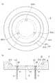
以下、本発明のエピタキシャルウェーハの製造方法の一実施態様について図面を参照しながら説明する。図1は、本発明のエピタキシャルウェーハの製造方法の一実施態様で使用される気相成長装置を模式的に示す断面図である。図2は、本発明のエピタキシャルウェーハの製造方法の一実施態様で使用されるサセプタを示す図で、(a)はサセプタの平面図であり、(b)はサセプタの縦断面図である。 Hereinafter, an embodiment of a method for producing an epitaxial wafer of the present invention will be described with reference to the drawings. FIG. 1 is a cross-sectional view schematically showing a vapor phase growth apparatus used in an embodiment of the epitaxial wafer manufacturing method of the present invention. 2A and 2B are views showing a susceptor used in an embodiment of the epitaxial wafer manufacturing method of the present invention. FIG. 2A is a plan view of the susceptor, and FIG. 2B is a longitudinal sectional view of the susceptor.
[気相成長装置]
まず、本発明のエピタキシャルウェーハの製造方法の一実施態様で使用される気相成長装置について説明する。本実施態様で使用される気相成長装置1は、図1に示すように、シリコンウェーハからなる半導体ウェーハWの主表面にエピタキシャル層EPを気相成長させて、エピタキシャルウェーハEWを製造する装置である。この気相成長装置1は、サセプタ2と、反応容器3と、加熱装置4と、リフトピン5とを備える。[Vapor phase growth equipment]
First, a vapor phase growth apparatus used in one embodiment of the epitaxial wafer manufacturing method of the present invention will be described. A vapor
反応容器3は、その内部にサセプタ2が設置され、かつその内部に反応ガスを供給することが可能なように構成されている。そして、反応容器3は、サセプタ2の上に載置された半導体ウェーハWに反応ガスを供給することで、半導体ウェーハWの主表面にエピタキシャル層EPを成長させる。この反応容器3は、上側ドーム31と、下側ドーム32と、ドーム取付体33、サセプタ支持部34とを備える。 The reaction vessel 3 has a
上側ドーム31及び下側ドーム32は、石英等の透光性部材から構成されている。 The
ドーム取付体33は、上方及び下方が開放された略筒状部材から構成され、上方側の開口部分及び下方側の開口部分にて上側ドーム31及び下側ドーム32を支持する。 The
このドーム取付体33の側面には、反応ガス供給管331が設けられており、反応ガス供給管331に対向するドーム取付体33の側面には、反応ガス排出管332が設けられている。反応ガス供給管331及び反応ガス排出管332は、反応容器3の内部と反応容器3の外部を連通するように形成されている。 A reaction
反応ガス供給管331からは、反応ガスが反応容器3の内部に供給される。反応ガスは、例えば、SiHCl3等のSiソースを水素ガスで希釈し、それにドーパントガスを微量混合してなる。供給された反応ガスは、サセプタ2に載置された半導体ウェーハWの主表面を水平に通過した後、反応ガス排出管332から反応容器3の外に排出される。A reaction gas is supplied into the reaction vessel 3 from the reaction
サセプタ2は、半導体ウェーハWを載置する部材であり、反応容器3の内部に設置される。サセプタ2は、回転軸Rに連なるサセプタ支持部34によって、その下面が支持され、回転軸Rの駆動により回転する。また、サセプタ2は、サセプタ支持部34が昇降することにより昇降する。サセプタ2の材質は特に限定されないが、例えば炭素基材の表面にSiC被膜をコーティングしたものが好ましい。 The
図1及び図2に示すように、サセプタ2の上面には、半導体ウェーハWの直径よりも大きい径で略円形の凹部からなるウェーハ載置部21が形成されている。ここで、略円形の形状は、真円形状に限定されず、楕円形状や真円に類似する形状が含まれる。このウェーハ載置部21は、第一凹部211と、第二凹部212とからなる。第一凹部211は、サセプタ2の上面から下側に凹んだ円形の凹部である。第二凹部212は、第一凹部211よりも小径で第一凹部211の底面から下側に凹んでおり、かつ、第一凹部211と同心の円形の凹部である。また、サセプタ2には、第二凹部212の外周縁側の位置に、第一凹部211の底面で半導体ウェーハWを支持するウェーハ支持部213が形成されている。 As shown in FIGS. 1 and 2, a
半導体ウェーハWは、ウェーハ支持部213に支持されることでウェーハ載置部21の内側に載置される。なお、ウェーハ支持部213は、第一凹部211の外周側から第二凹部212の外周側にかけて下方に傾斜する形状にして半導体ウェーハWの外周縁部を線接触で支持するようにしてもよく、あるいは、ウェーハ支持部213の上面に凹凸を設けて半導体ウェーハWの外周縁部を点接触で支持するようにしてもよい。 The semiconductor wafer W is placed on the inner side of the
サセプタ2へ半導体ウェーハWを搬入する際、又はサセプタ2から半導体ウェーハWを搬出する際は、半導体ウェーハWの下面をリフトピン5で支持してリフトピン5の昇降により半導体ウェーハWを昇降させる。 When the semiconductor wafer W is loaded into the
リフトピン5は、サセプタ2に内蔵される。リフトピン5は、頭部51が拡径され、この頭部51が半導体ウェーハWを載置するためのウェーハ載置部21の第二凹部212の底面に設けられた貫通孔22のテーパ状側壁部にぶら下がるように設置されている。 The
リフトピン5による半導体ウェーハWの着脱は、サセプタ2の昇降により行う。例えば、半導体ウェーハWをサセプタ2から取り外す場合、サセプタ2を下降させ、リフトピン5の尾部を反応容器3の下側ドーム32に当接させる。これによって付勢されたリフトピン5がその頭部51において半導体ウェーハWの裏面に突き当たり、半導体ウェーハWをウェーハ載置部21の上方に持ち上がる。この後、サセプタ2と半導体ウェーハWとの間にハンドラ(図示せず)が挿入され、半導体ウェーハWは、ハンドラに支えられて持ち上げられる。半導体ウェーハWは、ハンドラに支えられた状態で搬送され、次の工程に供される。 The semiconductor wafer W is attached / detached by the lift pins 5 by raising / lowering the
サセプタ支持部34は、石英等の透光性部材から構成され、図1に示すように、反応容器3の下側ドーム32の略中央部分から反応容器3の内部に突出し、サセプタ2を水平状態で反応容器3の内部に支持する。そして、サセプタ支持部34は、例えば、制御装置(図示せず)による制御のもと、回転軸Rを中心として回転自在、かつ回転軸Rの鉛直方向に昇降自在に構成されている。 The
加熱装置4は、反応容器3の上方側及び下方側にそれぞれ配設され、反応容器3の上側ドーム31及び下側ドーム32を介して、サセプタ2及びその上に設置された半導体ウェーハWを放射熱により加熱し、半導体ウェーハWを所定温度に設定するものである。この加熱装置4としては、例えば、ハロゲンランプや赤外ランプ等を採用できる。また、加熱装置4としては、放射熱により加熱するものの他、誘導加熱により半導体ウェーハWを加熱する高周波加熱方式を採用してもよい。 The
[エピタキシャルウェーハの製造方法]
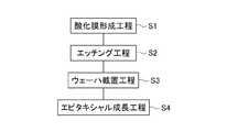
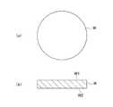
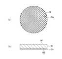
次に、本発明のエピタキシャルウェーハの製造方法の一実施態様について説明する。図3は、本発明のエピタキシャルウェーハの製造方法の一実施態様の工程を示す工程フロー図である。図4は、半導体ウェーハWの裏面W2に酸化膜を形成させる前の半導体ウェーハWを示す図で、(a)は底面図、(b)は縦断面図である。図5は、半導体ウェーハWの裏面W2の全体に酸化膜Oxを形成させた半導体ウェーハWを示す図で、(a)は底面図、(b)は縦断面図である。図6は、半導体ウェーハWの裏面W2の外周部分に酸化膜Oxを形成させた半導体ウェーハWを示す図で、(a)は底面図、(b)は縦断面図である。[Method of manufacturing epitaxial wafer]
Next, an embodiment of the method for producing an epitaxial wafer of the present invention will be described. FIG. 3 is a process flow diagram showing the steps of an embodiment of the method for producing an epitaxial wafer of the present invention. 4A and 4B are diagrams showing the semiconductor wafer W before an oxide film is formed on the back surface W2 of the semiconductor wafer W, where FIG. 4A is a bottom view and FIG. 4B is a longitudinal sectional view. 5A and 5B are views showing the semiconductor wafer W in which the oxide film Ox is formed on the entire back surface W2 of the semiconductor wafer W, where FIG. 5A is a bottom view and FIG. 5B is a longitudinal sectional view. 6A and 6B are diagrams showing a semiconductor wafer W in which an oxide film Ox is formed on the outer peripheral portion of the back surface W2 of the semiconductor wafer W, where FIG. 6A is a bottom view and FIG. 6B is a longitudinal sectional view.
本実施態様のエピタキシャルウェーハの製造方法は、半導体ウェーハWの裏面W2に酸化膜Oxからなる親水部を形成させる酸化膜形成工程S1と、酸化膜形成工程S1の後、酸化膜Oxの一部を半導体ウェーハWと同心の円形状に除去して、半導体ウェーハWの裏面W2が露出してなる疎水部Hpを設けるエッチング工程S2と、エッチング工程S2の後、半導体ウェーハWの裏面W2を下側にして、半導体ウェーハをウェーハ載置部21の内部に存在する半導体ウェーハ支持部213に載置するウェーハ載置工程S3と、ウェーハ載置工程S3の後、半導体ウェーハWの主表面W1にエピタキシャル層を成長させるエピタキシャル成長工程S4と、を備える。 In the epitaxial wafer manufacturing method of the present embodiment, an oxide film forming step S1 for forming a hydrophilic portion made of the oxide film Ox on the back surface W2 of the semiconductor wafer W, and a part of the oxide film Ox after the oxide film forming step S1. Etching step S2 for removing the semiconductor wafer W into a concentric circular shape and providing a hydrophobic portion Hp where the back surface W2 of the semiconductor wafer W is exposed, and after the etching step S2, the back surface W2 of the semiconductor wafer W is set downward. Then, after placing the semiconductor wafer on the semiconductor
本実施態様において使用される半導体ウェーハWは、以下で説明する酸化膜形成工程S1の前に、シリコン単結晶インゴットを所定の厚さにスライシングして作製される。半導体ウェーハWの直径は、例えば、200mm、300mm、450mm等である。スライシングした半導体ウェーハWは、表面がエッチング処理され、その後、主表面W1及び裏面W2に鏡面加工が施される。その後、以下に述べるように、酸化膜形成工程S1、エッチング工程S2、ウェーハ載置工程S3及びエピタキシャル成長工程S4が施される。 The semiconductor wafer W used in this embodiment is manufactured by slicing a silicon single crystal ingot to a predetermined thickness before an oxide film forming step S1 described below. The diameter of the semiconductor wafer W is, for example, 200 mm, 300 mm, 450 mm, or the like. The surface of the sliced semiconductor wafer W is etched, and then the main surface W1 and the back surface W2 are mirror-finished. Thereafter, as described below, an oxide film forming step S1, an etching step S2, a wafer mounting step S3, and an epitaxial growth step S4 are performed.
<酸化膜形成工程(S1)>
まず本実施態様の酸化膜形成工程S1について説明する。酸化膜形成工程S1は、半導体ウェーハWの裏面W2の全面に酸化膜Oxからなる親水部を形成させる工程である。具体的には、図4に示すような半導体ウェーハWの裏面W2を酸化作用のある薬液で処理することにより、図5に示すように半導体ウェーハWの裏面W2の全体に酸化膜Oxを形成させる工程である。<Oxide Film Formation Step (S1)>
First, the oxide film forming step S1 of this embodiment will be described. The oxide film forming step S1 is a step of forming a hydrophilic portion made of the oxide film Ox on the entire back surface W2 of the semiconductor wafer W. Specifically, the oxide film Ox is formed on the entire back surface W2 of the semiconductor wafer W as shown in FIG. 5 by processing the back surface W2 of the semiconductor wafer W as shown in FIG. It is a process.
酸化膜Oxは、バッチ式の洗浄装置や枚葉式の洗浄装置等を使用して、酸化作用のある薬液で処理することにより形成させる。酸化作用のある薬液(以下、単に「薬液」ともいう。)としては、半導体ウェーハWの裏面に酸化膜Oxを形成させることができれば特に限定されないが、例えば、純水にオゾンを含有させたオゾン水の他、SC(Standard Cleaning)−1液、SC−2液、HF−HNO3液、HF−H2O2液等、酸化作用のある各種洗浄液等が挙げられる。なお、SC−1液とは、NH4OH:H2O2:H2O=1:1:5の容量比で混合されている混合液である。また、SC−2液とは、HCl:H2O2:H2O=1:1:5の容量比で混合されている混合液である。The oxide film Ox is formed by processing with an oxidizing chemical solution using a batch type cleaning device, a single wafer type cleaning device, or the like. The chemical liquid having an oxidizing action (hereinafter also simply referred to as “chemical liquid”) is not particularly limited as long as the oxide film Ox can be formed on the back surface of the semiconductor wafer W. For example, ozone containing pure water containing ozone. In addition to water, SC (Standard Cleaning) -1 liquid, SC-2 liquid, HF-HNO3 liquid, HF-H2 O2 liquid, etc., various cleaning liquids having an oxidizing action and the like can be mentioned. Note that the SC-1solution, NH 4 OH: H 2 O 2: H 2 O = 1: 1: a mixture is mixed in a volume ratio of 5. The SC-2 solution is a mixed solution mixed at a volume ratio of HCl: H2 O2 : H2 O = 1: 1: 5.
酸化膜Oxは、半導体ウェーハWの裏面W2に設けられるが、必要に応じて、主表面W1に設けてもよい。この場合、裏面W2及び主表面W1に対して同時に酸化膜Oxを設けてもよいし、裏面W2及び主表面W1に対して別々に酸化膜Oxを設けてもよい。 The oxide film Ox is provided on the back surface W2 of the semiconductor wafer W, but may be provided on the main surface W1 as necessary. In this case, the oxide film Ox may be provided simultaneously on the back surface W2 and the main surface W1, or the oxide film Ox may be provided separately on the back surface W2 and the main surface W1.
酸化膜形成工程S1を経ることにより、例えば半導体ウェーハWがシリコンウェーハの場合、半導体ウェーハWの裏面W2は、疎水性のシリコン(Si)から、親水性の酸化シリコン(SiO2)に変化する。このとき、半導体ウェーハWの裏面W2に対する水の接触角は、20度以下であることが好ましく、10度以下であることがより好ましい。半導体ウェーハWの裏面W2に対する水の接触角が上限値以下であることにより、後に説明するエピタキシャル成長工程S4において、半導体ウェーハWとサセプタ2とが固着するスティッキング現象が効果的に防止され、エピタキシャルウェーハEWの外周部の歪みを抑制することができる。なお、半導体ウェーハWの裏面W2に自然酸化膜等が存在することにより、酸化膜形成工程S1を行う前に、半導体ウェーハWの裏面W2に対する水の接触角が上記の値を示す場合には、酸化膜形成工程S1が既に実施されたものとみなして、次のエッチング工程S2へ進んでもよい。Through the oxide film forming step S1, for example, when the semiconductor wafer W is a silicon wafer, the back surface W2 of the semiconductor wafer W is changed from hydrophobic silicon (Si) to hydrophilic silicon oxide (SiO2 ). At this time, the contact angle of water with respect to the back surface W2 of the semiconductor wafer W is preferably 20 degrees or less, and more preferably 10 degrees or less. Since the contact angle of water with the back surface W2 of the semiconductor wafer W is equal to or less than the upper limit value, the sticking phenomenon in which the semiconductor wafer W and the
なお、半導体ウェーハWに酸化膜Oxを設ける際、薬液の温度は、常温(室温)〜90℃であることが好ましい。また、半導体ウェーハWの裏面W2に対する接触角は、薬液の濃度、処理時間、薬液の温度等を調整することによって適宜変更することができる。 In addition, when providing the oxide film Ox in the semiconductor wafer W, it is preferable that the temperature of a chemical | medical solution is normal temperature (room temperature)-90 degreeC. Moreover, the contact angle with respect to the back surface W2 of the semiconductor wafer W can be appropriately changed by adjusting the concentration of the chemical solution, the processing time, the temperature of the chemical solution, and the like.
<エッチング工程(S2)>
次に本実施態様のエッチング工程S2について説明する。エッチング工程S2は、酸化膜形成工程S1で半導体ウェーハWの裏面W2に設けた酸化膜Oxからなる親水部の一部を、図6に示すように、半導体ウェーハWと同心の円形状に除去する工程である。エッチング工程S2を経ることにより、半導体ウェーハWの裏面W2に設けられた酸化膜Oxからなる親水部は、半導体ウェーハWの外周部分だけを残して除去される。<Etching step (S2)>
Next, the etching step S2 of this embodiment will be described. In the etching step S2, a part of the hydrophilic portion made of the oxide film Ox provided on the back surface W2 of the semiconductor wafer W in the oxide film formation step S1 is removed in a circular shape concentric with the semiconductor wafer W as shown in FIG. It is a process. Through the etching step S <b> 2, the hydrophilic portion made of the oxide film Ox provided on the back surface W <b> 2 of the semiconductor wafer W is removed leaving only the outer peripheral portion of the semiconductor wafer W.
エッチング工程S2は、例えばバッチ式の洗浄装置を使用して、半導体の酸化物(例えばSiO2)に対して腐食性のあるエッチング液で半導体ウェーハWの裏面W2を処理することにより行われる。ここで使用されるバッチ式の洗浄装置は、半導体ウェーハWを回転させる回転手段を備え、半導体ウェーハWを回転させながら、半導体ウェーハWの裏面W2側の中心付近に設けられた薬液吐出機構よりエッチング液を吐出させることができる。半導体ウェーハWの裏面W2の中心付近に吐出されたエッチング液は、半導体ウェーハWが回転するのに伴って、半導体ウェーハWの中心部から半導体ウェーハWの外周部に向かって、半導体ウェーハWと同心の円を描くように広がりながら移動する。このような作用により、半導体ウェーハWの内周側に存在する酸化膜Oxからなる親水部が半導体ウェーハWと同心の円形状に除去され、酸化膜Oxの下層に存在する疎水性の半導体(例えばSi)表面が露出する。The etching step S2 is performed by treating the back surface W2 of the semiconductor wafer W with an etchant that is corrosive to a semiconductor oxide (for example, SiO2 ) using, for example, a batch type cleaning apparatus. The batch-type cleaning apparatus used here includes a rotating means for rotating the semiconductor wafer W, and etching is performed by a chemical solution discharge mechanism provided near the center of the back surface W2 side of the semiconductor wafer W while rotating the semiconductor wafer W. The liquid can be discharged. The etchant discharged near the center of the back surface W2 of the semiconductor wafer W is concentric with the semiconductor wafer W from the center of the semiconductor wafer W toward the outer periphery of the semiconductor wafer W as the semiconductor wafer W rotates. Move while spreading to draw a circle. By such an action, the hydrophilic portion made of the oxide film Ox existing on the inner peripheral side of the semiconductor wafer W is removed in a circular shape concentric with the semiconductor wafer W, and a hydrophobic semiconductor (for example, the lower layer of the oxide film Ox (for example, Si) The surface is exposed.
上述のように、半導体ウェーハWの裏面W2に設けられた酸化膜Oxは、全面がエッチング液によって除去されるのではなく、半導体ウェーハWの内周側部分のみがエッチング液により除去され、半導体ウェーハWの外周側部分が残される。半導体ウェーハWの裏面W2に設けられた酸化膜Oxをこのように除去するには、バッチ式の洗浄装置における半導体ウェーハWの回転数を、通常の洗浄工程における回転数よりも小さく設定すればよい。半導体ウェーハWの回転数をどの程度に設定するかは、半導体ウェーハWの外周部に残される酸化膜Oxの大きさ、エッチング液の噴射量、エッチング液の粘度等によって変化するため、適宜条件に合わせて設定すればよい。半導体ウェーハWの外周部にどの程度酸化膜Oxを残すかについては、後述する。 As described above, the entire surface of the oxide film Ox provided on the back surface W2 of the semiconductor wafer W is not removed by the etching solution, but only the inner peripheral side portion of the semiconductor wafer W is removed by the etching solution. The outer peripheral side portion of W is left. In order to remove the oxide film Ox provided on the back surface W2 of the semiconductor wafer W in this way, the rotational speed of the semiconductor wafer W in the batch type cleaning apparatus may be set smaller than the rotational speed in the normal cleaning process. . The number of rotations of the semiconductor wafer W is set depending on the size of the oxide film Ox remaining on the outer periphery of the semiconductor wafer W, the amount of etching liquid sprayed, the viscosity of the etching liquid, etc. What is necessary is just to set. How much oxide film Ox is left on the outer periphery of the semiconductor wafer W will be described later.
半導体ウェーハWの裏面W2に設けられた酸化膜Oxを除去するためのエッチング液としては、半導体の酸化物(例えばSiO2)に対して腐食性のあるものであれば特に限定されない。このようなエッチング液としては、弗酸(HF)水溶液が例示される。エッチング液として使用される弗酸水溶液の濃度は、0.1〜10.0質量%が好ましく、0.5〜5.0質量%がより好ましい。An etching solution for removing the oxide film Ox provided on the back surface W2 of the semiconductor wafer W is not particularly limited as long as it is corrosive to a semiconductor oxide (for example, SiO2 ). An example of such an etchant is a hydrofluoric acid (HF) aqueous solution. The concentration of the hydrofluoric acid aqueous solution used as the etching solution is preferably 0.1 to 10.0% by mass, and more preferably 0.5 to 5.0% by mass.
既に述べたように、酸化膜Oxからなる親水部が除去されると、酸化膜Oxの下層に存在する疎水性の半導体(例えばSi)が露出して疎水部Hpを形成する。疎水部Hpでは、水の接触角が酸化膜Oxからなる親水部よりも大きくなるので、エッチング液により酸化膜Oxがどの程度の深さまで除去されたのかは、水の半導体表面に対する接触角を測定することにより把握することができる。酸化膜Oxが除去された後の半導体ウェーハ裏面W2の接触角としては、20度を超えることが好ましく、30度以上であることがより好ましい。接触角を上記の下限値以上とすることにより、サセプタ2に内蔵されたリフトピン5によるエピタキシャルウェーハEWの平坦度の低下が抑制される。 As already described, when the hydrophilic portion made of the oxide film Ox is removed, the hydrophobic semiconductor (for example, Si) existing under the oxide film Ox is exposed to form the hydrophobic portion Hp. In the hydrophobic part Hp, the contact angle of water is larger than that of the hydrophilic part made of the oxide film Ox. Therefore, the depth of the oxide film Ox removed by the etching solution is determined by measuring the contact angle of water with the semiconductor surface. This can be grasped. The contact angle of the semiconductor wafer back surface W2 after the oxide film Ox is removed is preferably more than 20 degrees, and more preferably 30 degrees or more. By making the contact angle equal to or greater than the above lower limit value, the flatness of the epitaxial wafer EW due to the lift pins 5 incorporated in the
次に、酸化膜形成工程S1によって半導体ウェーハWの裏面W2に設けられた酸化膜Oxのうち、エッチング工程S2で除去する範囲について説明する。既に述べたように、半導体ウェーハWの裏面W2に設けられた酸化膜Oxは、半導体ウェーハWの外周部分を残して内周部分が除去される。 Next, of the oxide film Ox provided on the back surface W2 of the semiconductor wafer W by the oxide film forming process S1, a range to be removed in the etching process S2 will be described. As already described, the inner peripheral portion of the oxide film Ox provided on the back surface W2 of the semiconductor wafer W is removed while leaving the outer peripheral portion of the semiconductor wafer W.
半導体ウェーハWの内周部分の酸化膜Oxを除去する理由は、ウェーハ載置部21に半導体ウェーハWが載置された際、半導体ウェーハWの裏面W2のうち、ウェーハ載置部21の第二凹部212に内蔵されたリフトピン5の上部にあたる箇所に酸化膜Oxが存在すると、作製されたエピタキシャルウェーハEWにおいて当該箇所の平坦度が低下するためである。すなわち、酸化膜Oxは、半導体ウェーハWの裏面W2へのプロセスガスの流入によって局所的にエッチングされる可能性があり、このような作用により半導体ウェーハWの裏面W2の平坦性の低下をもたらすおそれがある。このため、半導体ウェーハWの裏面W2に設けられた酸化膜Oxのうち、リフトピン5の上部に位置する酸化膜Oxを除去する必要がある。 The reason why the oxide film Ox on the inner peripheral portion of the semiconductor wafer W is removed is that the second of the
リフトピン5と酸化膜Oxとの位置関係について図2及び図7を使用して説明する。図7は、サセプタ2に半導体ウェーハWが載置された状態を示す図で、(a)は平面図、(b)は縦断面図である。 The positional relationship between the lift pins 5 and the oxide film Ox will be described with reference to FIGS. 7A and 7B are views showing a state in which the semiconductor wafer W is placed on the
リフトピン5は、ウェーハ載置部21の第二凹部212に、サセプタ2の中心から同一半径をなすように複数本(本実施態様の装置では3本)設けられる。したがって、複数本のリフトピン5は、第二凹部212の底面にサセプタ2と同心の仮想的なリフトピン設置円周LCを描くように設けられることになる。また、リフトピン5は、第二凹部212に設けられた貫通孔22に昇降可能に挿通されている。すなわち、第二凹部212の底面には、半導体ウェーハWを昇降させるリフトピン5を挿通させる貫通孔22がウェーハ載置部21と同心であるリフトピン設置円周LCの上に複数設けられることになる。 A plurality of lift pins 5 (three in the apparatus of the present embodiment) are provided in the
このとき、リフトピン設置円周LCの直径は、半導体ウェーハWの裏面W2に設けられた疎水部Hpの直径よりも小さい。したがって、リフトピン5の上部にあたる箇所には、半導体ウェーハWの裏面W2に設けられた疎水部Hpが存在する。このため、リフトピン5の上部に当たる箇所に酸化膜Oxが存在することに伴うエピタキシャルウェーハEWの平坦度の低下が抑制される。 At this time, the diameter of the lift pin installation circumference LC is smaller than the diameter of the hydrophobic portion Hp provided on the back surface W2 of the semiconductor wafer W. Accordingly, a hydrophobic portion Hp provided on the back surface W <b> 2 of the semiconductor wafer W exists at a location corresponding to the upper portion of the lift pins 5. For this reason, a decrease in the flatness of the epitaxial wafer EW due to the presence of the oxide film Ox at the location corresponding to the upper portion of the lift pins 5 is suppressed.
ここで、半導体ウェーハWの裏面W2の外周部に残される酸化膜Oxは、親水性を有する親水部でもある。本実施態様において、酸化膜Oxからなる親水部は、サセプタ2と半導体ウェーハWとの間のスティッキングを防止するため、半導体ウェーハWの裏面W2の外周部に十分な領域をもって設けられる。具体的には、酸化膜Oxからなる親水部が、半導体ウェーハWの裏面W2のうち、少なくともウェーハ載置部21の内部に存在する半導体ウェーハ支持部213と接する箇所に設けられることが好ましい。 Here, the oxide film Ox remaining on the outer peripheral portion of the back surface W2 of the semiconductor wafer W is also a hydrophilic portion having hydrophilicity. In this embodiment, the hydrophilic portion made of the oxide film Ox is provided with a sufficient area on the outer peripheral portion of the back surface W2 of the semiconductor wafer W in order to prevent sticking between the
半導体ウェーハWの裏面W2のうち、酸化膜Oxからなる親水部が残される領域は、具体的には、半導体ウェーハWの裏面W2のうち、半導体ウェーハWの外周縁より5mm内周側に位置する半導体ウェーハWと同心の円周と、半導体ウェーハWの外周縁との間の領域であることが好ましい。具体的には、図6において示される距離dが5mmとなる領域に酸化膜Oxからなる親水部が残されることが好ましい。 In the back surface W2 of the semiconductor wafer W, the region where the hydrophilic portion made of the oxide film Ox is left is specifically located on the inner peripheral side of 5 mm from the outer peripheral edge of the semiconductor wafer W in the back surface W2 of the semiconductor wafer W. A region between the circumference concentric with the semiconductor wafer W and the outer peripheral edge of the semiconductor wafer W is preferable. Specifically, it is preferable that a hydrophilic portion made of the oxide film Ox is left in a region where the distance d shown in FIG. 6 is 5 mm.
さらに具体的に説明するために、半導体ウェーハWの直径が300mm(半径150mm)である場合を例にとって説明する。この場合、半導体ウェーハWの裏面W2のうち、頭部51が約12mmに膨出したリフトピン5の中心部は、半径114mm付近に位置する。すなわち、半導体ウェーハWの裏面W2のうち、リフトピン5の上部にあたる箇所は、半導体ウェーハWの中心から108〜120mmの領域になる。したがって、半導体ウェーハWの中心から半径120mmの領域には、少なくとも酸化膜Oxが除去された疎水部Hpが設けられる。そして、半導体ウェーハWとサセプタ2とのスティッキングを防止するために、半導体ウェーハWの裏面W2のうち、半導体ウェーハWの中心から145〜150mmの領域に酸化膜Oxからなる親水部が設けられる。残りの領域である、半導体ウェーハWの裏面W2のうち、半導体ウェーハWの中心から120〜145mmの領域は、酸化膜Oxからなる親水部であっても疎水部Hpであってもよい。 In order to explain more specifically, the case where the diameter of the semiconductor wafer W is 300 mm (radius 150 mm) will be described as an example. In this case, the center part of the
<ウェーハ載置工程(S3)>
次に本実施態様のウェーハ載置工程S3について説明する。ウェーハ載置工程S3は、エッチング工程S2の後に行われる。この工程では、半導体ウェーハWの裏面W2を下側にして半導体ウェーハWをウェーハ載置部21に載置する。このとき、既に述べたように、半導体ウェーハWの裏面W2の外周部に設けられた酸化膜Oxがウェーハ支持部213に接触するように、半導体ウェーハWをウェーハ載置部21に載置する。<Wafer placement process (S3)>
Next, the wafer mounting step S3 of this embodiment will be described. The wafer placement process S3 is performed after the etching process S2. In this step, the semiconductor wafer W is mounted on the
半導体ウェーハWをウェーハ載置部21に載置する方法は、特に限定されず、公知の種々の方法で半導体ウェーハWを載置させることができる。 The method for placing the semiconductor wafer W on the
<エピタキシャル成長工程(S4)>
エピタキシャル成長工程S4は、ウェーハ載置工程S3の後に行う。エピタキシャル成長は、反応ガスを反応ガス供給管331から反応容器3の内側へ導入し、1000〜1200℃の高温に熱せられた半導体ウェーハWの主表面W1に、反応ガスの熱分解又は還元によって生成された、例えばシリコン(Si)を0.5〜6.0μm/分で成長させることにより行われる。反応ガスは、例えばSiソースであるSiHCl3を水素ガスに混合させることにより調製される。反応ガスには、必要に応じてドーパントガスが添加される。<Epitaxial growth step (S4)>
The epitaxial growth step S4 is performed after the wafer placement step S3. The epitaxial growth is generated by thermal decomposition or reduction of the reaction gas on the main surface W1 of the semiconductor wafer W introduced into the reaction vessel 3 from the reaction
これにより、半導体ウェーハWの主表面W1にエピタキシャル層EPが成長し、エピタキシャルウェーハEWが得られる。 Thereby, the epitaxial layer EP grows on the main surface W1 of the semiconductor wafer W, and the epitaxial wafer EW is obtained.
エピタキシャル成長工程S4の後、エピタキシャルウェーハEWの裏面W2の外周部に酸化膜Oxが形成されたままで次工程を行う。または、エピタキシャル成長工程S4の後、エピタキシャルウェーハEWの裏面W2の酸化膜OxをHF溶液、BHF溶液、DHF溶液等を用いて洗浄し、酸化膜Oxを除去してもよい。これにより、酸化膜Oxを有していないエピタキシャルウェーハEWが作製される。 After the epitaxial growth step S4, the next step is performed while the oxide film Ox is formed on the outer peripheral portion of the back surface W2 of the epitaxial wafer EW. Alternatively, after the epitaxial growth step S4, the oxide film Ox on the back surface W2 of the epitaxial wafer EW may be cleaned using an HF solution, a BHF solution, a DHF solution, or the like to remove the oxide film Ox. Thereby, the epitaxial wafer EW not having the oxide film Ox is produced.
本実施態様のエピタキシャルウェーハの製造方法によれば、以下の効果が奏される。 According to the epitaxial wafer manufacturing method of the present embodiment, the following effects can be obtained.
本実施態様のエピタキシャルウェーハの製造方法は、上面に半導体ウェーハWを載置する略円形で凹状のウェーハ載置部21を有するとともに、底面に半導体ウェーハWを昇降させるリフトピン5を挿通させる貫通孔22をウェーハ載置部21と同心であるリフトピン設置円周LCの上に複数有するサセプタ2を備えた気相成長装置1を用い、半導体ウェーハWの裏面W2に酸化膜Oxからなる親水部を形成させる酸化膜形成工程S1と、酸化膜形成工程S1の後、酸化膜Oxの一部を半導体ウェーハWと同心の円形状に除去して、半導体ウェーハWの裏面W2が露出してなる疎水部Hpを設けるエッチング工程S2と、エッチング工程S2の後、半導体ウェーハWの裏面W2を下側にして、半導体ウェーハWをウェーハ載置部21に載置するウェーハ載置工程S3と、ウェーハ載置工程S3の後、半導体ウェーハWの主表面W1にエピタキシャル層EPを成長させるエピタキシャル成長工程S4と、を備え、リフトピン設置円周LCの直径は、疎水部Hpの直径よりも小さい。 The epitaxial wafer manufacturing method of this embodiment has a substantially circular and concave
そのため、半導体ウェーハWの外周部分に酸化膜Oxが存在し、エピタキシャル成長工程S4における半導体ウェーハWとサセプタ2との間のスティッキングが防止される。したがって、スティッキングが存在することに伴う半導体ウェーハWとサセプタ2との間の熱膨張率の違いを原因とする半導体ウェーハWの歪みが防止される。また、ウェーハ載置部21に内蔵されたリフトピン5の上部に、半導体ウェーハWの裏面W2に設けられた酸化膜Oxは存在しないので、作製されたエピタキシャルウェーハEWの平坦性が良好に維持される。 Therefore, the oxide film Ox exists on the outer peripheral portion of the semiconductor wafer W, and sticking between the semiconductor wafer W and the
また、本実施態様のエピタキシャルウェーハの製造方法は、酸化膜Oxからなる親水部が半導体ウェーハWの裏面W2のうち、少なくともウェーハ載置部21と接する箇所に設けられる。 In the epitaxial wafer manufacturing method according to the present embodiment, the hydrophilic portion made of the oxide film Ox is provided at least on the back surface W <b> 2 of the semiconductor wafer W in contact with the
そのため、半導体ウェーハWは、常に酸化膜Oxからなる親水部でサセプタ2と接することになるので、半導体ウェーハWとサセプタ2との間のスティッキングが防止される。したがって、スティッキングが存在することに伴う半導体ウェーハWとサセプタ2との間の熱膨張率の違いを原因とする半導体ウェーハWの歪みが防止される。 For this reason, the semiconductor wafer W is always in contact with the
以上、本発明の実施態様について図面を参照しながら詳細に説明したが、本発明は、以上の実施態様に何ら限定されるものではなく、本発明の目的の範囲内において、適宜変更を加えて実施することができる。 The embodiments of the present invention have been described in detail with reference to the drawings. However, the present invention is not limited to the above embodiments, and appropriate modifications are made within the scope of the object of the present invention. Can be implemented.
例えば、サセプタ2のウェーハ載置部21は、第二凹部212を有していなくてもよい。すなわち、ウェーハ載置部21は、1段の凹部でもよい。この場合、当該凹部の底面にリフトピン及びリフトピンを挿通するための貫通孔が設けられることになる。 For example, the
また、上記実施態様は、半導体の例としてシリコンを用いて説明したが、本発明で使用される半導体は、シリコンに制限されない。 Moreover, although the said embodiment demonstrated using silicon as an example of a semiconductor, the semiconductor used by this invention is not restrict | limited to silicon.
以下、実施例により本発明をさらに詳細に説明するが、本発明はこれらの実施例に限定されるものではない。 EXAMPLES Hereinafter, although an Example demonstrates this invention further in detail, this invention is not limited to these Examples.
[実施例1]
両面が研磨された直径300mmでp型のシリコンウェーハを枚葉式の洗浄機に設置し、酸化膜形成工程として、そのシリコンウェーハを1000rpmで回転させながら主表面及び裏面にオゾン水溶液(濃度20ppm)を流量1SLMで1分間噴射させることにより、シリコンウェーハの主表面及び裏面に酸化膜を形成させた。次に、エッチング工程として、シリコンウェーハの回転数を10rpmとし、裏面に弗酸水溶液(濃度1質量%)を流量1SLMで1分間噴射して、シリコンウェーハの裏面に形成させた酸化膜を、シリコンウェーハの外周部分を残して除去した。その後、シリコンウェーハの主表面及び裏面に純水を噴射して洗浄した。なお、オゾン水溶液及び弗酸水溶液の噴出ノズルは、シリコンウェーハの略中心部に設置されており、これらのノズルとシリコンウェーハの裏面との間の距離は、5mmである。[Example 1]
A 300 mm diameter p-type silicon wafer polished on both sides is placed in a single wafer cleaning machine, and as an oxide film formation process, an ozone aqueous solution (concentration 20 ppm) is applied to the main surface and back surface while rotating the silicon wafer at 1000 rpm. Was sprayed at a flow rate of 1 SLM for 1 minute to form oxide films on the main surface and the back surface of the silicon wafer. Next, as an etching process, the rotational speed of the silicon wafer is set to 10 rpm, and an aqueous hydrofluoric acid solution (
上記処理により、シリコンウェーハの裏面の酸化膜は、シリコンウェーハの中心から125〜150mmの領域(すなわち、シリコンウェーハの外周25mmの領域)を残して除去された。酸化膜が残された箇所の水の接触角は10度以下(中心から148mm)であり、酸化膜が除去された箇所の水の接触角は40度(中心から114mmであり、サセプタ上のリフトピンが存在する箇所)であった。 By the above process, the oxide film on the back surface of the silicon wafer was removed leaving a region of 125 to 150 mm from the center of the silicon wafer (that is, a region of 25 mm outer periphery of the silicon wafer). The contact angle of water where the oxide film is left is 10 degrees or less (148 mm from the center), and the contact angle of water where the oxide film is removed is 40 degrees (114 mm from the center). ).
上記処理により得られたシリコンウェーハを、裏面が下側になるように、エピタキシャル成長装置に設けられたサセプタのウェーハ載置部に載置して、シリコンウェーハの主表面にエピタキシャル層を成長させた。エピタキシャル成長用の反応ガスは、SiHCl3と水素ガスとを混合したガスに、p型ドーパントとしてB2H6を添加したものを使用し、反応ガス供給管から反応容器の内部に導入した。シリコンウェーハを1130℃に熱し、エピタキシャル層を反応速度2.5μm/minで、3μmの厚さに成長させた。The silicon wafer obtained by the above treatment was placed on the wafer placing portion of the susceptor provided in the epitaxial growth apparatus so that the back surface was on the lower side, and an epitaxial layer was grown on the main surface of the silicon wafer. As a reaction gas for epitaxial growth, a gas obtained by mixing SiHCl3 and hydrogen gas with B2H6 added as a p-type dopant was used and introduced into the reaction vessel through a reaction gas supply pipe. The silicon wafer was heated to 1130 ° C., and the epitaxial layer was grown to a thickness of 3 μm at a reaction rate of 2.5 μm / min.
得られたエピタキシャルウェーハの裏面の外周部歪みをSIRD(Scanning InfraRed Depolarization)(テプラ社製SIRD A300)を用いて測定したところ、外周部歪みが存在しないことが確認された。 When the distortion of the outer peripheral portion of the back surface of the obtained epitaxial wafer was measured using SIRD (Scanning InfraRed Depolarization) (SIRD A300 manufactured by Tepla), it was confirmed that there was no peripheral strain.
また、得られたエピタキシャルウェーハの平坦性をWaferSight(KLA−Tencor社製)を用いて測定したところ、良好な平坦性を有することが確認され、リフトピンが存在することに伴う平坦性の低下現象が防止されたことを確認した。 Further, when the flatness of the obtained epitaxial wafer was measured using WaferSight (manufactured by KLA-Tencor), it was confirmed that it had good flatness, and there was a phenomenon that flatness was lowered due to the presence of lift pins. Confirmed that it was prevented.
[実施例2]
エッチング工程の条件を、シリコンウェーハの回転数を30rpm、弗酸水溶液の噴射時間を1分間としたこと以外は、実施例1と同じ条件にて酸化膜形成工程及びエッチング工程を行った。[Example 2]
The oxide film forming step and the etching step were performed under the same conditions as those in Example 1 except that the rotation speed of the silicon wafer was 30 rpm and the spray time of the hydrofluoric acid aqueous solution was 1 minute.
上記処理により、シリコンウェーハの裏面の酸化膜は、シリコンウェーハの中心から145〜150mmの領域(すなわち、シリコンウェーハの外周5mmの領域)を残して除去された。酸化膜が残された箇所(中心から148mm)の水の接触角は10度以下であり、酸化膜が除去された箇所(中心から114mmであり、サセプタ上のリフトピンが存在する箇所)の水の接触角は40度であった。 By the above process, the oxide film on the back surface of the silicon wafer was removed leaving a region of 145 to 150 mm from the center of the silicon wafer (that is, a region of the outer periphery of the silicon wafer of 5 mm). The contact angle of water at the place where the oxide film is left (148 mm from the center) is 10 degrees or less, and the water at the place where the oxide film is removed (place where the lift pin on the susceptor is 114 mm from the center) The contact angle was 40 degrees.
上記処理により得られたシリコンウェーハを、実施例1と同じ条件によりエピタキシャル成長させ、外周部歪み及び平坦性の評価を行った。その結果、実施例1と同様に、得られたエピタキシャルウェーハの裏面の外周部歪み及び平坦性は良好だった。 The silicon wafer obtained by the above treatment was epitaxially grown under the same conditions as in Example 1, and the peripheral portion distortion and flatness were evaluated. As a result, similar to Example 1, the peripheral portion distortion and flatness of the back surface of the obtained epitaxial wafer were good.
[比較例1]
エッチング工程の条件を、シリコンウェーハの回転数を50rpm、弗酸水溶液の噴射時間を10分間としたこと以外は、実施例1と同じ条件にて酸化膜形成工程及びエッチング工程を行った。[Comparative Example 1]
The oxide film forming step and the etching step were performed under the same conditions as in Example 1, except that the rotation speed of the silicon wafer was 50 rpm and the spray time of the hydrofluoric acid aqueous solution was 10 minutes.
上記処理により、シリコンウェーハの裏面の水の接触角がシリコンウェーハの裏面全面に亘り40度以上となり、シリコンウェーハの裏面の酸化膜は全て剥離されたことが確認された。 As a result of the above treatment, it was confirmed that the water contact angle on the back surface of the silicon wafer was 40 degrees or more over the entire back surface of the silicon wafer, and the oxide film on the back surface of the silicon wafer was all peeled off.
上記処理により得られたシリコンウェーハを、実施例1と同じ条件によりエピタキシャル成長させ、外周部歪み及び平坦性の評価を行った。その結果、得られたエピタキシャルウェーハの裏面の外周部歪みは不良であることが確認されたが、平坦性は良好だった。 The silicon wafer obtained by the above treatment was epitaxially grown under the same conditions as in Example 1, and the peripheral portion distortion and flatness were evaluated. As a result, it was confirmed that the distortion of the outer peripheral portion of the back surface of the obtained epitaxial wafer was poor, but the flatness was good.
[比較例2]
酸化膜形成工程を行った後、エッチング工程を行わなかったこと以外は、実施例1と同じ条件によりエピタキシャル成長させ、外周部及び平坦性の評価を行った。その結果、得られたエピタキシャルウェーハの裏面の外周部歪みは良好であったが、平坦性はリフトピンの存在箇所にて不良だった。[Comparative Example 2]
After performing the oxide film forming step, the outer peripheral portion and the flatness were evaluated by epitaxial growth under the same conditions as in Example 1 except that the etching step was not performed. As a result, the distortion of the outer peripheral portion of the back surface of the obtained epitaxial wafer was good, but the flatness was poor at the location where the lift pins were present.
以上の結果、エピタキシャル成長を行う前に、シリコンウェーハの裏面の外周部だけに酸化膜を形成させる前処理を行うことにより、エピタキシャルウェーハの外周部歪みの発生防止と、リフトピンが存在する箇所における平坦性の低下の防止とが両立可能なことが示された。 As a result of the above, by performing a pretreatment to form an oxide film only on the outer peripheral part of the back surface of the silicon wafer before epitaxial growth, the occurrence of distortion of the outer peripheral part of the epitaxial wafer and the flatness where the lift pins are present It was shown that it is possible to achieve both the prevention of the decrease in the level.
1 気相成長装置
2 サセプタ
21 ウェーハ載置部
211 第一凹部
212 第二凹部
213 ウェーハ支持部
22 貫通孔
3 反応容器
5 リフトピン
EP エピタキシャル層
EW エピタキシャルウェーハ
Hp 疎水部
LC リフトピン設置円周
Ox 酸化膜(親水部)
S1 酸化膜形成工程
S2 エッチング工程
S3 ウェーハ載置工程
S4 エピタキシャル成長工程
W 半導体ウェーハ
W1 主表面
W2 裏面DESCRIPTION OF
S1 Oxide film formation process S2 Etching process S3 Wafer mounting process S4 Epitaxial growth process W Semiconductor wafer W1 Main surface W2 Back surface
Claims (4)
Translated fromJapanese前記半導体ウェーハの裏面に酸化膜からなる親水部を形成させる酸化膜形成工程と、
前記酸化膜形成工程の後、前記酸化膜の一部を前記半導体ウェーハと同心の円形状に除去して、半導体ウェーハの裏面が露出してなる疎水部を設けるエッチング工程と、
前記エッチング工程の後、前記半導体ウェーハの裏面を下側にして、前記半導体ウェーハを前記ウェーハ載置部に載置するウェーハ載置工程と、
前記ウェーハ載置工程の後、前記半導体ウェーハの主表面にエピタキシャル層を成長させるエピタキシャル成長工程と、を備え、
前記リフトピン設置円周の直径は、前記疎水部の直径よりも小さいことを特徴とするエピタキシャルウェーハの製造方法。The upper surface has a substantially circular and concave wafer mounting portion for mounting the semiconductor wafer, and the bottom surface has a lift pin installation circumference that is concentric with the wafer mounting portion and through which a lift pin for raising and lowering the semiconductor wafer is inserted. A method for producing an epitaxial wafer using a vapor phase growth apparatus provided with a plurality of susceptors above,
An oxide film forming step of forming a hydrophilic portion made of an oxide film on the back surface of the semiconductor wafer;
After the oxide film forming step, an etching step of removing a part of the oxide film in a circular shape concentric with the semiconductor wafer and providing a hydrophobic portion in which the back surface of the semiconductor wafer is exposed;
After the etching step, with the back surface of the semiconductor wafer facing down, a wafer mounting step of mounting the semiconductor wafer on the wafer mounting portion,
An epitaxial growth step for growing an epitaxial layer on the main surface of the semiconductor wafer after the wafer mounting step; and
The method of manufacturing an epitaxial wafer, wherein a diameter of the lift pin installation circumference is smaller than a diameter of the hydrophobic portion.
前記貫通孔は、前記第二凹部の底面に設けられ、
前記ウェーハ載置工程では、前記半導体ウェーハの裏面の外周縁部が前記半導体ウェーハ支持部に支持されるように、前記半導体ウェーハを前記ウェーハ支持部に載置する請求項1又は請求項2記載のエピタキシャルウェーハの製造方法。The wafer mounting portion has a circular first recess recessed downward from the upper surface of the susceptor, and has a smaller diameter than the first recess and is recessed downward from the bottom surface of the first recess. And a concentric circular second recess, and a semiconductor wafer support portion for supporting the semiconductor wafer at the bottom surface of the first recess is formed at a position on the outer peripheral edge side of the second recess.
The through hole is provided on the bottom surface of the second recess,
The said wafer mounting process WHEREIN: The said semiconductor wafer is mounted in the said wafer support part so that the outer periphery edge part of the back surface of the said semiconductor wafer may be supported by the said semiconductor wafer support part. Epitaxial wafer manufacturing method.
Priority Applications (2)
| Application Number | Priority Date | Filing Date | Title |
|---|---|---|---|
| JP2008327274AJP5141541B2 (en) | 2008-12-24 | 2008-12-24 | Epitaxial wafer manufacturing method |
| US12/645,744US7960254B2 (en) | 2008-12-24 | 2009-12-23 | Manufacturing method for epitaxial wafer |
Applications Claiming Priority (1)
| Application Number | Priority Date | Filing Date | Title |
|---|---|---|---|
| JP2008327274AJP5141541B2 (en) | 2008-12-24 | 2008-12-24 | Epitaxial wafer manufacturing method |
Publications (2)
| Publication Number | Publication Date |
|---|---|
| JP2010153433A JP2010153433A (en) | 2010-07-08 |
| JP5141541B2true JP5141541B2 (en) | 2013-02-13 |
Family
ID=42266735
Family Applications (1)
| Application Number | Title | Priority Date | Filing Date |
|---|---|---|---|
| JP2008327274AActiveJP5141541B2 (en) | 2008-12-24 | 2008-12-24 | Epitaxial wafer manufacturing method |
Country Status (2)
| Country | Link |
|---|---|
| US (1) | US7960254B2 (en) |
| JP (1) | JP5141541B2 (en) |
Families Citing this family (18)
| Publication number | Priority date | Publication date | Assignee | Title |
|---|---|---|---|---|
| WO2009060913A1 (en)* | 2007-11-08 | 2009-05-14 | Sumco Corporation | Method for manufacturing epitaxial wafer |
| JP2010016312A (en)* | 2008-07-07 | 2010-01-21 | Sumco Corp | Method for manufacturing epitaxial wafer |
| JP5412759B2 (en)* | 2008-07-31 | 2014-02-12 | 株式会社Sumco | Epitaxial wafer holder and method for manufacturing the wafer |
| JP2011082443A (en)* | 2009-10-09 | 2011-04-21 | Sumco Corp | Epitaxial wafer and method for manufacturing the same |
| JP5540919B2 (en)* | 2010-06-16 | 2014-07-02 | 住友電気工業株式会社 | Method for cleaning silicon carbide semiconductor |
| US8535445B2 (en)* | 2010-08-13 | 2013-09-17 | Veeco Instruments Inc. | Enhanced wafer carrier |
| US10163676B2 (en) | 2013-06-27 | 2018-12-25 | Taiwan Semiconductor Manufacturing Co., Ltd. | Apparatus and system for preventing backside peeling defects on semiconductor wafers |
| EP3100298B1 (en) | 2014-01-27 | 2020-07-15 | Veeco Instruments Inc. | Wafer carrier having retention pockets with compound radii for chemical vapor deposition systems |
| WO2015179081A1 (en) | 2014-05-21 | 2015-11-26 | Applied Materials, Inc. | Thermal processing susceptor |
| CN116200821A (en)* | 2016-03-28 | 2023-06-02 | 应用材料公司 | Base support |
| KR102528559B1 (en)* | 2016-07-26 | 2023-05-04 | 삼성전자주식회사 | Apparatus for manufacturing a large size substrate |
| US20180102247A1 (en)* | 2016-10-06 | 2018-04-12 | Asm Ip Holding B.V. | Substrate processing apparatus and method of manufacturing semiconductor device |
| DE102017212799A1 (en)* | 2017-07-26 | 2019-01-31 | Siltronic Ag | Epitaxially coated semiconductor wafer of monocrystalline silicon and process for its preparation |
| JP7083699B2 (en)* | 2018-05-25 | 2022-06-13 | 信越半導体株式会社 | Evaluation method |
| JP7188250B2 (en)* | 2019-04-11 | 2022-12-13 | 株式会社Sumco | Vapor deposition apparatus and carrier used therefor |
| KR102640172B1 (en) | 2019-07-03 | 2024-02-23 | 삼성전자주식회사 | Processing apparatus for a substrate and method of driving the same |
| JP7192756B2 (en)* | 2019-12-19 | 2022-12-20 | 株式会社Sumco | Vapor deposition apparatus and vapor deposition method |
| JP2023134139A (en)* | 2022-03-14 | 2023-09-27 | キオクシア株式会社 | Semiconductor manufacturing device |
Family Cites Families (9)
| Publication number | Priority date | Publication date | Assignee | Title |
|---|---|---|---|---|
| JPS63137418A (en)* | 1986-11-28 | 1988-06-09 | Nec Kansai Ltd | Epitaxial growing method |
| US6971835B2 (en)* | 2001-12-21 | 2005-12-06 | Sumitomo Mitsubishi Silicon Corporation | Vapor-phase epitaxial growth method |
| JP4066881B2 (en)* | 2003-05-21 | 2008-03-26 | 信越半導体株式会社 | Surface treatment method, silicon epitaxial wafer manufacturing method, and silicon epitaxial wafer |
| JP4292872B2 (en)* | 2003-05-29 | 2009-07-08 | 信越半導体株式会社 | Manufacturing method of silicon epitaxial wafer |
| WO2005001916A1 (en)* | 2003-06-26 | 2005-01-06 | Shin-Etsu Handotai Co., Ltd. | Method for producing silicon epitaxial wafer and silicon epitaxial wafer |
| JP4400331B2 (en) | 2004-06-17 | 2010-01-20 | 信越半導体株式会社 | Wafer shape evaluation method and management method |
| US8021484B2 (en)* | 2006-03-30 | 2011-09-20 | Sumco Techxiv Corporation | Method of manufacturing epitaxial silicon wafer and apparatus therefor |
| JP5444607B2 (en) | 2007-10-31 | 2014-03-19 | 株式会社Sumco | Epitaxial film forming apparatus susceptor, epitaxial film forming apparatus, and epitaxial wafer manufacturing method |
| JP5012554B2 (en) | 2008-02-19 | 2012-08-29 | 株式会社Sumco | Epitaxial wafer manufacturing method |
- 2008
- 2008-12-24JPJP2008327274Apatent/JP5141541B2/enactiveActive
- 2009
- 2009-12-23USUS12/645,744patent/US7960254B2/enactiveActive
Also Published As
| Publication number | Publication date |
|---|---|
| US7960254B2 (en) | 2011-06-14 |
| US20100159679A1 (en) | 2010-06-24 |
| JP2010153433A (en) | 2010-07-08 |
Similar Documents
| Publication | Publication Date | Title |
|---|---|---|
| JP5141541B2 (en) | Epitaxial wafer manufacturing method | |
| JP5444607B2 (en) | Epitaxial film forming apparatus susceptor, epitaxial film forming apparatus, and epitaxial wafer manufacturing method | |
| JP4798163B2 (en) | Epitaxial growth susceptor | |
| JP5092975B2 (en) | Epitaxial wafer manufacturing method | |
| JP5604907B2 (en) | Semiconductor substrate support susceptor for vapor phase growth, epitaxial wafer manufacturing apparatus, and epitaxial wafer manufacturing method | |
| WO2005034219A1 (en) | Production method for silicon epitaxial wafer, and silicon epitaxial wafer | |
| JP2010016312A (en) | Method for manufacturing epitaxial wafer | |
| TWI626730B (en) | Method of manufacturing epitaxial wafer | |
| JP5195370B2 (en) | Epitaxial wafer manufacturing method | |
| JP5161748B2 (en) | Vapor growth susceptor, vapor growth apparatus, and epitaxial wafer manufacturing method | |
| JP5098873B2 (en) | Susceptor and vapor phase growth apparatus for vapor phase growth apparatus | |
| JPWO2009060913A1 (en) | Epitaxial wafer manufacturing method | |
| TW201005803A (en) | Silicon epitaxial wafer and method for manufacturing the same | |
| JP3541838B2 (en) | Susceptor and apparatus and method for manufacturing epitaxial wafer | |
| JP2006041028A (en) | Susceptor and epitaxial wafer manufacturing method | |
| JP4675749B2 (en) | Epitaxial wafer manufacturing method | |
| JP2010040574A (en) | Production process of epitaxial wafer, and epitaxial wafer | |
| JP2009176959A (en) | Susceptor, vapor phase growing apparatus, and vapor phase growing method | |
| JP5272377B2 (en) | Epitaxial wafer manufacturing method | |
| JP2010027881A (en) | Method of manufacturing epitaxial wafer | |
| JP5140990B2 (en) | Epitaxial silicon wafer manufacturing method | |
| JP2004349405A (en) | Surface treatment method, silicon epitaxial wafer and method of manufacturing the same | |
| JP5144697B2 (en) | Susceptor, epitaxial wafer manufacturing apparatus, and epitaxial wafer manufacturing method | |
| JP2010034113A (en) | Vapor deposition device | |
| JP4591824B2 (en) | Susceptor |
Legal Events
| Date | Code | Title | Description |
|---|---|---|---|
| A621 | Written request for application examination | Free format text:JAPANESE INTERMEDIATE CODE: A621 Effective date:20111216 | |
| A977 | Report on retrieval | Free format text:JAPANESE INTERMEDIATE CODE: A971007 Effective date:20121017 | |
| TRDD | Decision of grant or rejection written | ||
| A01 | Written decision to grant a patent or to grant a registration (utility model) | Free format text:JAPANESE INTERMEDIATE CODE: A01 Effective date:20121023 | |
| A01 | Written decision to grant a patent or to grant a registration (utility model) | Free format text:JAPANESE INTERMEDIATE CODE: A01 | |
| A61 | First payment of annual fees (during grant procedure) | Free format text:JAPANESE INTERMEDIATE CODE: A61 Effective date:20121105 | |
| FPAY | Renewal fee payment (event date is renewal date of database) | Free format text:PAYMENT UNTIL: 20151130 Year of fee payment:3 | |
| R150 | Certificate of patent or registration of utility model | Free format text:JAPANESE INTERMEDIATE CODE: R150 Ref document number:5141541 Country of ref document:JP Free format text:JAPANESE INTERMEDIATE CODE: R150 | |
| R250 | Receipt of annual fees | Free format text:JAPANESE INTERMEDIATE CODE: R250 | |
| R250 | Receipt of annual fees | Free format text:JAPANESE INTERMEDIATE CODE: R250 | |
| R250 | Receipt of annual fees | Free format text:JAPANESE INTERMEDIATE CODE: R250 | |
| R250 | Receipt of annual fees | Free format text:JAPANESE INTERMEDIATE CODE: R250 | |
| R250 | Receipt of annual fees | Free format text:JAPANESE INTERMEDIATE CODE: R250 | |
| R250 | Receipt of annual fees | Free format text:JAPANESE INTERMEDIATE CODE: R250 | |
| R250 | Receipt of annual fees | Free format text:JAPANESE INTERMEDIATE CODE: R250 | |
| R250 | Receipt of annual fees | Free format text:JAPANESE INTERMEDIATE CODE: R250 | |
| R250 | Receipt of annual fees | Free format text:JAPANESE INTERMEDIATE CODE: R250 | |
| R250 | Receipt of annual fees | Free format text:JAPANESE INTERMEDIATE CODE: R250 |