JP5137546B2 - Image sensor control unit, electronic endoscope, and endoscope system - Google Patents
Image sensor control unit, electronic endoscope, and endoscope systemDownload PDFInfo
- Publication number
- JP5137546B2 JP5137546B2JP2007315071AJP2007315071AJP5137546B2JP 5137546 B2JP5137546 B2JP 5137546B2JP 2007315071 AJP2007315071 AJP 2007315071AJP 2007315071 AJP2007315071 AJP 2007315071AJP 5137546 B2JP5137546 B2JP 5137546B2
- Authority
- JP
- Japan
- Prior art keywords
- image sensor
- light
- endoscope
- cmos image
- signal
- Prior art date
- Legal status (The legal status is an assumption and is not a legal conclusion. Google has not performed a legal analysis and makes no representation as to the accuracy of the status listed.)
- Active
Links
- 238000005286illuminationMethods0.000claimsdescription21
- 238000001514detection methodMethods0.000claimsdescription16
- 239000013307optical fiberSubstances0.000claimsdescription11
- 230000003287optical effectEffects0.000claimsdescription8
- 238000003384imaging methodMethods0.000claimsdescription7
- 230000005855radiationEffects0.000claims2
- 238000003780insertionMethods0.000description7
- 230000037431insertionEffects0.000description7
- 238000010586diagramMethods0.000description6
- 238000009825accumulationMethods0.000description4
- 210000001260vocal cordAnatomy0.000description3
- 230000003321amplificationEffects0.000description2
- 230000001678irradiating effectEffects0.000description2
- 238000004519manufacturing processMethods0.000description2
- 238000003199nucleic acid amplification methodMethods0.000description2
- 238000006243chemical reactionMethods0.000description1
- 238000009792diffusion processMethods0.000description1
- 230000000694effectsEffects0.000description1
- 229910052736halogenInorganic materials0.000description1
- 150000002367halogensChemical class0.000description1
- 239000011159matrix materialSubstances0.000description1
- 238000000034methodMethods0.000description1
- 229910052724xenonInorganic materials0.000description1
- FHNFHKCVQCLJFQ-UHFFFAOYSA-Nxenon atomChemical compound[Xe]FHNFHKCVQCLJFQ-UHFFFAOYSA-N0.000description1
Images


Classifications
- A—HUMAN NECESSITIES
- A61—MEDICAL OR VETERINARY SCIENCE; HYGIENE
- A61B—DIAGNOSIS; SURGERY; IDENTIFICATION
- A61B1/00—Instruments for performing medical examinations of the interior of cavities or tubes of the body by visual or photographical inspection, e.g. endoscopes; Illuminating arrangements therefor
- A61B1/04—Instruments for performing medical examinations of the interior of cavities or tubes of the body by visual or photographical inspection, e.g. endoscopes; Illuminating arrangements therefor combined with photographic or television appliances
- A61B1/05—Instruments for performing medical examinations of the interior of cavities or tubes of the body by visual or photographical inspection, e.g. endoscopes; Illuminating arrangements therefor combined with photographic or television appliances characterised by the image sensor, e.g. camera, being in the distal end portion
- H—ELECTRICITY
- H04—ELECTRIC COMMUNICATION TECHNIQUE
- H04N—PICTORIAL COMMUNICATION, e.g. TELEVISION
- H04N23/00—Cameras or camera modules comprising electronic image sensors; Control thereof
- H04N23/50—Constructional details
- H04N23/555—Constructional details for picking-up images in sites, inaccessible due to their dimensions or hazardous conditions, e.g. endoscopes or borescopes
- H—ELECTRICITY
- H04—ELECTRIC COMMUNICATION TECHNIQUE
- H04N—PICTORIAL COMMUNICATION, e.g. TELEVISION
- H04N23/00—Cameras or camera modules comprising electronic image sensors; Control thereof
- H04N23/60—Control of cameras or camera modules
- H04N23/667—Camera operation mode switching, e.g. between still and video, sport and normal or high- and low-resolution modes
- H—ELECTRICITY
- H04—ELECTRIC COMMUNICATION TECHNIQUE
- H04N—PICTORIAL COMMUNICATION, e.g. TELEVISION
- H04N23/00—Cameras or camera modules comprising electronic image sensors; Control thereof
- H04N23/70—Circuitry for compensating brightness variation in the scene
- H—ELECTRICITY
- H04—ELECTRIC COMMUNICATION TECHNIQUE
- H04N—PICTORIAL COMMUNICATION, e.g. TELEVISION
- H04N23/00—Cameras or camera modules comprising electronic image sensors; Control thereof
- H04N23/70—Circuitry for compensating brightness variation in the scene
- H04N23/74—Circuitry for compensating brightness variation in the scene by influencing the scene brightness using illuminating means
- H—ELECTRICITY
- H04—ELECTRIC COMMUNICATION TECHNIQUE
- H04N—PICTORIAL COMMUNICATION, e.g. TELEVISION
- H04N25/00—Circuitry of solid-state image sensors [SSIS]; Control thereof
- H04N25/50—Control of the SSIS exposure
- H04N25/53—Control of the integration time
- H04N25/531—Control of the integration time by controlling rolling shutters in CMOS SSIS
- H—ELECTRICITY
- H04—ELECTRIC COMMUNICATION TECHNIQUE
- H04N—PICTORIAL COMMUNICATION, e.g. TELEVISION
- H04N25/00—Circuitry of solid-state image sensors [SSIS]; Control thereof
- H04N25/50—Control of the SSIS exposure
- H04N25/53—Control of the integration time
- H04N25/532—Control of the integration time by controlling global shutters in CMOS SSIS
Landscapes
- Engineering & Computer Science (AREA)
- Multimedia (AREA)
- Signal Processing (AREA)
- Health & Medical Sciences (AREA)
- Life Sciences & Earth Sciences (AREA)
- Surgery (AREA)
- Biomedical Technology (AREA)
- Molecular Biology (AREA)
- Optics & Photonics (AREA)
- Pathology (AREA)
- Radiology & Medical Imaging (AREA)
- Biophysics (AREA)
- Physics & Mathematics (AREA)
- Heart & Thoracic Surgery (AREA)
- Medical Informatics (AREA)
- Nuclear Medicine, Radiotherapy & Molecular Imaging (AREA)
- Animal Behavior & Ethology (AREA)
- General Health & Medical Sciences (AREA)
- Public Health (AREA)
- Veterinary Medicine (AREA)
- Transforming Light Signals Into Electric Signals (AREA)
- Endoscopes (AREA)
- Studio Devices (AREA)
- Instruments For Viewing The Inside Of Hollow Bodies (AREA)
Description
Translated fromJapanese本発明は、照明光の発光パターンに応じてCMOS撮像素子を適切に駆動する撮像素子制御ユニットに関する。The present invention relatesto an image sensor control unit thatappropriately drives a CMOS image sensorin accordance with a light emission pattern of illumination light .
挿入管の先端に撮像素子を設けた電子内視鏡が知られている。光源から放射される照明光を光ファイバによって挿入管の先端に伝達することにより、光の到達しない体内や構造物内の被写体を撮像することが可能である。 An electronic endoscope in which an image sensor is provided at the tip of an insertion tube is known. By transmitting the illumination light emitted from the light source to the distal end of the insertion tube through an optical fiber, it is possible to image a subject in the body or structure where the light does not reach.
被写体への照明光の照射方法によっては、特殊な画像を表示することが可能になる。例えば、周期的に発光と停止とを繰返すパルス発光により被写体を照射することが知られている。声帯を撮像するときに、声帯の振動の周波数と略同じ周波数でパルス発光を行い、その反射光を撮像することにより、高速で振動する声帯を低速で振動しているように表示することが可能である。 Depending on the method of illuminating the subject, a special image can be displayed. For example, it is known to irradiate a subject by pulse light emission that periodically repeats light emission and stop. When imaging the vocal cords, it is possible to display the vocal cords that vibrate at high speed as if they vibrated at low speed by emitting pulses at approximately the same frequency as the vocal cord vibration frequency and imaging the reflected light. It is.
パルス発光を行なう場合には高速で動く被写体を撮像することが多いため、全画素に同じ期間に受光させることが好ましい。一方で、照明光を常に被写体に照射する定常発光を行なう場合には静止物や低速で動く被写体が撮像されることが多いため、ノイズの影響の少ない画像信号を得ることが好ましい。 When performing pulsed light emission, a subject moving at high speed is often imaged. Therefore, it is preferable that all pixels receive light during the same period. On the other hand, when performing steady light emission that always irradiates a subject with illumination light, a stationary object or a subject that moves at low speed is often imaged. Therefore, it is preferable to obtain an image signal that is less affected by noise.
ノイズの影響が少なく且つグローバル露光により被写体を撮像するために従来の電子内視鏡ではCCD撮像素子を用いられていた。しかし、CCD撮像素子は、製造コストが高いこと、駆動電圧が高いこと、接続の必要な信号線数が多いなどの課題を有していた。 In order to pick up an image of a subject with little influence of noise and global exposure, a CCD image pickup device is used in a conventional electronic endoscope. However, the CCD image pickup device has problems such as high manufacturing cost, high drive voltage, and a large number of signal lines that need to be connected.
そこで、最近では製造コストや電力消費量の観点においてCCD撮像素子より有利なCMOS撮像素子を電子内視鏡に用いることが提案されている(特許文献1参照)。しかし、CMOS撮像素子では、グローバル露光を行うときに画像のS/Nが劣化していた。それゆえ、パルス発光による照明光を照射した被写体を撮るためにCMOS撮像素子にグローバル露光を行なわせていると、定常発光させたときに撮像する画像がノイズにより乱れることが問題であった。
したがって、本発明では、パルス発光および定常発光のように複数の発光パターンに応じて適切にCMOS撮像素子を駆動する撮像素子駆動ユニットの提供を目的とする。 Accordingly, an object of the present invention is to provide an image sensor driving unit that appropriately drives a CMOS image sensor in accordance with a plurality of light emission patterns such as pulsed light emission and steady light emission.
本発明の撮像素子駆動ユニットは、内視鏡に設けられるCMOS撮像素子を制御する撮像素子制御ユニットであって、CMOS撮像素子に撮像させる被写体に照射する照明光を発光する光源からの照明光の照射パターンを検出する検出部と、検出部が検出した照射パターンが第1の発光パターンである場合にはCMOS撮像素子にグローバル露光を実行させ照射パターンが第2の発光パターンである場合にはCMOS撮像素子にライン露光を実行させる露光制御部とを備えることを特徴としている。 An image sensor drive unit according to the present invention is an image sensor control unit that controls a CMOS image sensor provided in an endoscope, and is configured to emit illumination light from a light source that emits illumination light that irradiates a subject to be imaged by the CMOS image sensor. A detection unit for detecting an irradiation pattern, and if the irradiation pattern detected by the detection unit is the first light emission pattern, the CMOS image sensor is subjected to global exposure, and if the irradiation pattern is the second light emission pattern, the CMOS And an exposure control unit that causes the image sensor to perform line exposure.
なお、第1の発光パターンはパルス発光であることが好ましく、また第2の発光パターンは定常発光であることが好ましい。 Note that the first light emission pattern is preferably pulsed light emission, and the second light emission pattern is preferably steady light emission.
本発明の電子内視鏡は、CMOS撮像素子と、CMOS撮像素子に撮像させる被写体に照射する照明光を発光する光源からの照明光の照射パターンを検出する検出部と、検出部が検出した照射パターンが第1の発光パターンである場合にはCMOS撮像素子にグローバル露光を実行させ照射パターンが第2の発光パターンである場合にはCMOS撮像素子にライン露光を実行させる露光制御部とを備えることを特徴としている。 An electronic endoscope according to the present invention includes a CMOS image sensor, a detection unit that detects an irradiation pattern of illumination light from a light source that emits illumination light that is emitted to a subject to be imaged by the CMOS image sensor, and an irradiation detected by the detection unit An exposure control unit that performs global exposure on the CMOS image sensor when the pattern is the first light emission pattern and causes the CMOS image sensor to perform line exposure when the irradiation pattern is the second light emission pattern; It is characterized by.
本発明の内視鏡システムは、CMOS撮像素子が設けられる内視鏡と、CMOS撮像素子に撮像させる被写体に照射する照明光を発光する光源からの照明光の照射パターンを検出する検出部と、検出部が検出した照射パターンがパルス発光である場合にはCMOS撮像素子にグローバルシャッタ機能を実行させ照射パターンが定常発光である場合にはCMOS撮像素子にグローバルシャッタ機能を停止させるシャッタ機能切替え部とを備えることを特徴としている。 An endoscope system of the present invention includes an endoscope provided with a CMOS image sensor, a detection unit that detects an illumination pattern of illumination light from a light source that emits illumination light that is emitted to a subject to be imaged by the CMOS image sensor, A shutter function switching unit that executes a global shutter function for the CMOS image sensor when the irradiation pattern detected by the detection unit is pulsed light emission, and stops the global shutter function for the CMOS image sensor when the irradiation pattern is steady light emission; It is characterized by having.
本発明によれば、光源の発光パターンに応じてCMOS撮像素子にグローバル露光またはライン露光を実行させることが可能である。 According to the present invention, it is possible to cause the CMOS image sensor to perform global exposure or line exposure according to the light emission pattern of the light source.
以下、本発明の実施形態について図面を参照して説明する。
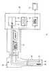
図1は、本発明の一実施形態を適用した撮像素子制御ユニットを有する内視鏡システムの内部構成を概略的に示すブロック図である。Embodiments of the present invention will be described below with reference to the drawings.
FIG. 1 is a block diagram schematically showing an internal configuration of an endoscope system having an image sensor control unit to which an embodiment of the present invention is applied.
内視鏡システム10は、内視鏡プロセッサ20、電子内視鏡30、およびモニタ11によって構成される。内視鏡プロセッサ20は、電子内視鏡30、及びモニタ11に接続される。 The
内視鏡プロセッサ20から被写体に照射するための照明光が電子内視鏡30に供給される。照明光を照射された被写体が電子内視鏡30により撮像される。電子内視鏡30の撮像により生成する画像信号が内視鏡プロセッサ20に送られる。 Illumination light for irradiating the subject from the
内視鏡プロセッサ20では、電子内視鏡30から得られた画像信号に対して所定の信号処理が施される。所定の信号処理を施した画像信号はモニタ11に送信され、送信された画像信号に相当する画像がモニタ11に表示される。 In the
内視鏡プロセッサ20には光源ユニット21、画像信号処理回路22、およびシステムコントローラ23などが設けられる。後述するように、光源ユニット21は被写体に照射する照明光をライトガイド31の入射端に放射する。また、後述するように、画像信号処理回路22では画像信号に対して所定の信号処理が施される。システムコントローラ23により内視鏡システム10全体の動作が制御される。 The
電子内視鏡30をコネクタ37を介して内視鏡プロセッサ20に接続すると、光源ユニット21と電子内視鏡30に設けられるライトガイド31とが光学的に接続される。また、内視鏡プロセッサ20と電子内視鏡30とを接続すると、画像信号処理回路22と電子内視鏡30に設けられる撮像素子32とが、内視鏡プロセッサ20に設けられるシステムコントローラ23と撮像素子駆動回路33とが電気的に接続される。 When the
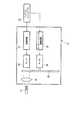
図2に示すように、光源ユニット21は、ランプ24、ロータリーシャッタ25、集光レンズ26、電源回路27、モータ28、およびロータリーシャッタ駆動回路29などによって構成される。 As shown in FIG. 2, the
ランプ24は、例えばキセノンランプやハロゲンランプであり、白色光を出射する。ランプ24から出射される白色光をライトガイド31の入射端に導くための光路中にロータリーシャッタ25および集光レンズ26が設けられる。 The
ロータリーシャッタ25は円板上に開口部と遮光部とが設けられる。光源ユニット21から白色光を放射するときには、光路上に開口部が挿入される。一方、白色光の放射を停止するときには、光路上に遮光部が挿入され、遮光される。モータ28を回転させることにより、光源ユニット21からの白色光の放射と放射停止とが切替えられる。また、光路上に開口部を挿入することにより、白色光が光源ユニット21から放射されたまま維持される。 The
なお、モータ28は、ロータリーシャッタ駆動回路29により駆動される。また、ロータリーシャッタ駆動回路29は、システムコントローラ23に制御される。 The
集光レンズ26により、光源ユニット21から放射される白色光が集光され、ライトガイド31の入射端に入射する。 White light emitted from the
ランプ24には、電源回路27から電力が供給される。電源回路27からのランプ24への電力の供給のON/OFFは、システムコントローラ23により制御される。 Electric power is supplied to the
次に電子内視鏡30の構成について詳細に説明する(図1参照)。電子内視鏡30には、ライトガイド31、撮像素子32、撮像素子駆動回路(露光制御部)32、光検出部34、配光レンズ35、および対物レンズ36などが設けられる。 Next, the configuration of the
内視鏡プロセッサ20との接続部分から延びるライトガイド31は、コネクタ37内において分岐する。ライトガイド31は光ファイバのバンドルであって、一部の光ファイバはコネクタ37に設けられる光検出部34に接続される。残りの光ファイババンドルは電子内視鏡30の挿入管38の先端まで延設される。 The
前述のように光源ユニット21から出射される白色光がライトガイド31の入射端に入射される。入射端に入射された光は、光検出部34および挿入管38先端の出射端まで伝達される。 As described above, the white light emitted from the
光検出部34により光源ユニット21の発光パターンが、パルス発光および定常発光のいずれの発光パターンであるかが検出される。検出した発光パターンは撮像素子駆動回路33に通知される。発光パターンがパルス発光である場合には、撮像素子駆動回路33はグローバル露光指令信号を撮像素子 に送信する。または、発光パターンが定常発光である場合には、撮像素子駆動回路33はライン露光指令信号を撮像素子32に送信する。なお、撮像素子駆動回路33は、システムコントローラ23により制御される。 The
ライトガイド31の挿入管側の出射端から出射する光が、配光レンズ35を介して挿入管38先端付近に照射される。白色光が照射されたときの被写体の反射光による光学像が、対物レンズ36を介して撮像素子32の受光面に到達する。撮像素子駆動回路33の駆動に従って、撮像素子32は、受光面に到達した光学像に対応する画像信号を生成する。 Light exiting from the exit end of the
撮像素子32は、CMOS撮像素子である。図3に示すように、撮像素子32の受光面には行列状に複数の画素40が配置される。各画素40において受光量に応じた画素信号が生成される。画素信号は、順番に出力部32oを介して読出される。受光面全面の画素50が生成する画素信号の集合によって画像信号が形成される。なお、画素信号を出力させる画素50は、行選択回路32rおよび列選択回路32cによって選択される。 The
図4を用いて、各画素40の内部構成を以下に説明する。図4は、画素の内部構成を示す回路図である。画素40は、フォトダイオード(PD)41、フローティングディフュージョン(FD)42、シャッタトランジスタ43、リセットトランジスタ44、増幅トランジスタ45、行選択トランジスタ46によって構成される。 The internal configuration of each
PD41が光電変換することにより受光量に応じた信号電荷が生成される。シャッタトランジスタ43をONにすることにより、PD41が生成した信号電荷はFD42に転送され、FD42において電荷に応じた信号電位に変換される。 The signal charge corresponding to the amount of received light is generated by the photoelectric conversion of the
なお、シャッタトランジスタ43は、行毎に別々のシャッタ信号線(図示せず)に接続される。行毎にシャッタ信号ΦSHがHIGHに切替えられる。シャッタ信号ΦSHがHIGHに切替えられるときに、シャッタトランジスタ43はONになり、導通状態となる。 The
リセットトランジスタ44をONにすることにより、FD42がリセットされ、FD42に蓄積された信号電荷が電圧源Vddに掃出され、FD41の電位は電圧源Vddの電位にリセットされる。By the
なお、リセットトランジスタ44は、行毎に別々のリセット信号線(図示せず)に接続される。リセット信号線には、行毎にHIGHまたはLOWに切替えられるリセット信号ΦRが流される。リセット信号ΦRがHIGHであるときに、リセットトランジスタ44はONになり、導通状態となる。 The
増幅トランジスタ45により、FDの電位に応じた画素信号が行選択トランジスタ46に出力される。行選択トランジスタ46をONに切替えられるときに、画素信号は垂直読出し線32vに出力される。 A pixel signal corresponding to the potential of the FD is output to the
垂直読出し線32vは同じ列に並ぶすべての画素40に接続される。行選択トランジスタ46を行毎に別々にONにすることにより、同じ列の垂直読出し線32vに接続される画素40の画素信号を別々に出力することが可能である。The
なお、行選択トランジスタ46は、行毎に別々の行選択信号線(図示せず)に接続されており、行毎に行選択信号ΦSLがHIGHに切替えられる。行選択信号ΦSLがHIGHに切替えられる間、行選択トランジスタ46はON、すなわち導通状態となる。 The
各列の垂直読出し線32vは、列選択トランジスタ32csを介して、水平読出し線32hに接続される。各列の列選択トランジスタ32csが順番にONに切替えられることにより、各列の垂直読出し線32vに出力された画素信号が水平読出し線32hおよび出力部32oを介して画像信号処理回路22に出力される。 The
各行のシャッタトランジスタ43、リセットトランジスタ44、および行選択トランジスタ46のON/OFFの切替えは、行選択回路32rによって制御される。列選択トランジスタ32csのON/OFFの切替えは、列選択回路32cによって制御される。 ON / OFF switching of the
行選択回路32rおよび列選択回路32cは、撮像素子駆動回路33から送信されるクロック信号などの撮像素子32の駆動のための信号に基づいて、上述の信号線ΦSH、ΦR、ΦSL、ΦSCのHIGH/LOWの切替を行なう。 The
なお、行選択回路32rおよび列選択回路32cはグローバル露光指令信号を受信したときには、グローバル露光を実行するようにトランジスタのON/OFFの切替を行なう。または、ライン露光指令信号を受信したときには、ライン露光を実行するようにトランジスタのON/OFFの切替を行なう。 When the
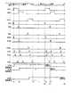
上述のような構成である撮像素子32の動作について、図5、図6のタイミングチャートを用いて説明する。図5は、ライン露光を実行するときの撮像素子32の動作を示すタイミングチャートである。図6は、グローバル露光を実行するときの撮像素子32の動作を示すタイミングチャートである。 The operation of the
システムコントローラ22から撮像素子駆動回路33に、周期的にHIGH/LOWが切替わるフレーム信号が送信される。フレーム信号がHIGHまたはLOWである期間中に撮像素子32の受光面全体の画素40から画素信号が生成され、読出される。 A frame signal for periodically switching HIGH / LOW is transmitted from the
ライン露光を実行する場合の動作について説明する。第1のフレーム期間中のタイミングt1において第1のシャッタ信号ΦSH1がHIGHに切替えられ、PD41に蓄積された信号電荷がFD42に転送される。信号電荷の転送が終わり第1のシャッタ信号ΦSH1がLOWに切替わった後に、1行目の画素40のPD41において信号電荷の蓄積が始まる。 An operation when line exposure is performed will be described. At timing t1 during the first frame period, the first shutter signal ΦSH1 is switched to HIGH, and the signal charge accumulated in the
タイミングt1の後であって、第1のフレーム期間中のタイミングt2において第2のシャッタ信号ΦSH2がHIGHに切替えられ、PD41に蓄積された信号電荷がFD42に転送される。信号電荷の転送が終わり第2のシャッタ信号ΦSH2がLOWに切替わった後に、2行目の画素40のPD41において信号電荷の蓄積が始まる。 After timing t1, the second shutter signal ΦSH2 is switched to HIGH at timing t2 in the first frame period, and the signal charge accumulated in the
以後、第1のフレーム期間中にそれぞれの行に対応するシャッタ信号ΦSHが順番にHIGH/LOWの切替わることにより、各行の画素40のPD41において信号電荷の蓄積が始まる。 Thereafter, during the first frame period, the shutter signal ΦSH corresponding to each row is sequentially switched between HIGH / LOW, whereby signal charge accumulation starts in the
第1のフレーム期間における最終行の画素信号の読出しが終わると、第1のフレーム期間が終了し、第2のフレーム期間が開始される(タイミングt3参照)。信号電荷を十分に蓄積させるための所定の期間p経過後のタイミングt4において1行目のリセット信号ΦR1がHIGHに切替えられ(ΦR1欄参照)、1行目の全画素40におけるリセットトランジスタ44がONになる。リセットトランジスタ44をONにすることにより、FD42がリセットされ、FD42に蓄積されていた信号電荷が電圧源Vddに掃出される。 When the reading of the pixel signals of the last row in the first frame period is finished, the first frame period is finished and the second frame period is started (see timing t3). The reset signal ΦR1 in the first row is switched to HIGH (see the ΦR1 column) at a timing t4 after a predetermined period p for sufficiently storing the signal charge (see the ΦR1 column), and the
1行目の画素40のリセット終了後のタイミングt5において、1行目の行選択信号ΦSL1がHIGHに切替えられ(ΦSL1欄参照)、1行目の全画素40の行選択トランジスタ46がONになる。 At timing t5 after the reset of the
1行目の画素40の行選択トランジスタ46がONになることにより、1行目の画素40からの画素信号の読出しが可能となる。なお、後述するように、1行目の全列の画素信号が読出されるまで、1行目の行選択信号ΦSL1はHIGIに維持される。 When the
また、タイミングt5の直後に、、第1のシャッタ信号ΦSH1がHIGHに切替わり(ΦSH1欄参照)、タイミングt1からタイミングt5のまでの間にPD41に蓄積された信号電荷(1行目画素信号欄符号S参照)がFD42に転送される。 Immediately after the timing t5, the first shutter signal ΦSH1 is switched to HIGH (see the ΦSH1 column), and the signal charges accumulated in the
信号電荷のFD42への転送が終わると、1列目から最終列であるn列目(nは正の整数)の列選択信号ΦSC1〜ΦSCnが順番にHIGHに切替えられ、1〜n列目の列選択トランジスタ32csが順番にONになる。したがって、1行目のすべての画素信号が1〜n列目まで順番に撮像素子32から読出される。 When the transfer of the signal charges to the
1行n列目の画素信号が読出されると、1行目の行選択信号ΦSL1はLOWに、2行目のリセット信号ΦR2がHIGHに切替えられる(タイミングt6参照)。1行目と同様に、2行目の画素40のFD42がリセットされる。リセット後2行目の行選択信号ΦSL2がHIGHに切替えられ、2行目の画素40からの画素信号の読出しが可能となる。 When the pixel signal in the first row and the nth column is read, the row selection signal ΦSL1 in the first row is switched to LOW, and the reset signal ΦR2 in the second row is switched to HIGH (see timing t6). Similar to the first row, the
1行目と同様に、2行目の行選択信号ΦSL2がHIGHに切替えられた直後のタイミングt7において、第2のシャッタ信号ΦSH2がHIGHに切替わり(ΦSH2欄参照)、タイミングt2からタイミングt7までの間にPD41に蓄積された信号電荷(2行目画素信号欄符号S参照)がFD42に転送される。また、1行目と同様にして、2行目のすべての画素信号が順番に撮像素子32から読出される。 Similar to the first row, at the timing t7 immediately after the row selection signal ΦSL2 of the second row is switched to HIGH, the second shutter signal ΦSH2 is switched to HIGH (see the ΦSH2 column), and from the timing t2 to the timing t7. Signal charges (see pixel signal column code S in the second row) accumulated in the
以後、3行目から最終行であるm行目まで順番に、1、2行目と同様の操作が行なわれる。m行目の画素信号の読出しを終えると(タイミングt8参照)、フレーム信号がLOWに切替わる。フレーム信号が切替わるときに、1画像の撮像が終了し、次のフレームの画像の撮像が始まる。 Thereafter, the same operations as those in the first and second lines are performed in order from the third line to the last m-th line. When the reading of the pixel signal of the m-th row is completed (see timing t8), the frame signal is switched to LOW. When the frame signal is switched, the imaging of one image is completed and the imaging of the next frame image is started.
次にグローバル露光を実行する場合の動作について説明する。第1のフレーム期間中のタイミングt1において第1〜第mのシャッタ信号ΦSH1〜ΦSHmが同時にHIGHに切替えられ、全行のPD41に蓄積された信号電荷がFD42に転送される。信号電荷の転送が終わり第1〜第mのシャッタ信号ΦSH1〜ΦSHmがLOWに切替わった後に、全行の画素40のPD41において信号電荷の蓄積が始まる。 Next, the operation when performing global exposure will be described. At timing t1 in the first frame period, the first to mth shutter signals ΦSH1 to ΦSHm are simultaneously switched to HIGH, and the signal charges accumulated in the
第1のフレーム期間における最終行の画素信号の読出しが終わると、第1のフレーム期間が終了し、第2のフレーム期間が開始される(タイミングt2参照)。ライン露光と同様に、信号電荷を十分に蓄積させるための所定の期間p経過後のタイミングt3において全行のリセット信号ΦR1〜ΦRmがHIGHに切替えられ(ΦR1〜ΦRm欄参照)、全画素40のFD42に蓄積されていた信号電荷が電圧源Vddに掃出される。 When reading of the pixel signals of the last row in the first frame period is finished, the first frame period is finished and the second frame period is started (see timing t2). Similar to the line exposure, the reset signals ΦR1 to ΦRm of all the rows are switched to HIGH (see the ΦR1 to ΦRm columns) at the timing t3 after the elapse of a predetermined period p for sufficiently storing the signal charges (see the ΦR1 to ΦRm columns) The signal charge accumulated in the
全画素40のリセット終了後のタイミングt4において、1行目の行選択信号ΦSL1がHIGHに切替えられ(ΦSL1欄参照)、1行目の全画素40の行選択トランジスタ46がONになる。 At timing t4 after completion of resetting of all the
1行目の画素40の行選択トランジスタ46がONになることにより、1行目の画素40からの画素信号の読出しが可能となる。なお、後述するように、1行目の全列の画素信号が読出されるまで、1行目の行選択信号ΦSL1はHIGIに維持される。 When the
また、タイミングt4において、第1〜第mのシャッタ信号ΦSH1〜ΦSHmがHIGHに切替わり(ΦSH1〜ΦSHm欄参照)、タイミングt1からタイミングt4までの間にPD41に蓄積された信号電荷(1行目〜m行目画素信号欄符号S参照)がFD42に転送される。 Further, at timing t4, the first to mth shutter signals ΦSH1 to ΦSHm are switched to HIGH (see the ΦSH1 to ΦSHm column), and the signal charges accumulated in the
信号電荷のFD42への転送が終わると、1列目から最終列であるn列目(nは正の整数)の列選択信号ΦSC1〜ΦSCnが順番にHIGHに切替えられ、1〜n列目の列選択トランジスタ32csが順番にONになる。したがって、1行目のすべての画素信号が1〜n列目まで順番に撮像素子32から読出される。 When the transfer of the signal charges to the
1行n列目の画素信号が読出されると、1行目の行選択信号ΦSL1はLOWに切替えられ、その後、2行目の行選択信号ΦSL2がHIGHに切替えられる(タイミングt5、t6参照)。 When the pixel signal of the first row and the nth column is read, the row selection signal ΦSL1 of the first row is switched to LOW, and then the row selection signal ΦSL2 of the second row is switched to HIGH (see timings t5 and t6). .
1行目と異なり、2行目の行選択信号ΦSL2がHIGHの間には第2のシャッタ信号ΦSH2はLOWのまま維持される。したがって、タイミングt6以降においてもFD42にはタイミングt4において転送された信号電荷が保持されている。Unlike the first row,the second shutter signal ΦSH2 is kept LOW while the row selection signal ΦSL2 of the second row is HIGH. Therefore, the signal charge transferred at the timing t4 is held in the
1行目と同様に1〜n列目の列選択信号ΦSC1〜ΦSCnが順番にHIGHに切替えられ、1〜n列目の列選択トランジスタが順番にONになる。したがって、2行目のすべての画素信号が1〜n列目まで順番に撮像素子32から読出される。 As in the first row, the column selection signals ΦSC1 to ΦSCn in the 1st to nth columns are sequentially switched to HIGH, and the column selection transistors in the 1st to nth columns are sequentially turned on. Accordingly, all the pixel signals in the second row are read from the
以後、3〜m行目の行選択信号ΦSL3〜ΦSLmが順番にHIGHに切替えられる。3〜m行目の行選択信号ΦSL3〜ΦSLmがそれぞれHIGHに切替えられている間には、2行目と同様に、FD42への転送とを行なうこと無く、1〜n列目の列選択信号ΦSC1〜ΦSCnが順番にHIGHに切替えられる。したがって、3〜m行目の画素信号も、1〜n列目まで順番に撮像素子32から読出される。Thereafter, the row selection signals ΦSL3 to ΦSLm of the 3rd to 3rd rows are sequentially switched to HIGH. While the row selection signals ΦSL3 to ΦSLm of the 3rd to mth rows are respectively switched to HIGH, the column selection of the 1st to nth columns is performed without performing the transfer to the
以上のように、本実施形態の撮像素子制御ユニットによれば、光源の発光パターンに応じてグローバル露光またはライン露光をCMOS撮像素子に実行させて、被写体を撮像することが可能である。 As described above, according to the image sensor control unit of the present embodiment, the subject can be imaged by causing the CMOS image sensor to perform global exposure or line exposure according to the light emission pattern of the light source.
前述のように、パルス発光をする場合には、高速で動く被写体を撮像することが多いので、受光面全体で同時期に光学像を撮像することが好ましい。本実施形態によれば、パルス発光時を検出して、CMOS撮像素子にグローバル露光を実行させるので、画像の歪みを低減化させるように撮像することが可能になる。 As described above, when pulse light emission is performed, an object that moves at high speed is often imaged. Therefore, it is preferable to capture an optical image on the entire light receiving surface at the same time. According to the present embodiment, when the pulse emission is detected and the CMOS image sensor is caused to perform global exposure, it is possible to perform imaging so as to reduce image distortion.
一方、前述のように、定常発光をする場合には、ノイズの影響の少ない画像を撮像することが求められる。グローバル露光を行なうときには、FD42への信号電荷の転送時期から読出し時期までの時間が長くなる行があるため、暗電流などの固定パターンノイズが増大する。しかし、定常発光時を検出して、CMOS撮像素子32にライン露光を実行させるので、画像のノイズを低減化することが可能になる。 On the other hand, as described above, when steady light emission is performed, it is required to capture an image with less influence of noise. When performing global exposure, there is a line in which the time from the transfer timing of the signal charge to the
なお、本実施形態では、パルス発光時にグローバル露光を実行させ、定常発光時にライン露光を実行させる構成であるが、光源の発光パターンに応じてグローバル露光またはライン露光を切替えれば、本実施形態と同様の効果が得られる。動体の歪みを抑えることが好ましい場合にはグローバル露光に、ノイズの低減化が好ましい場合にはライン露光に切替えられればよい。 In this embodiment, the global exposure is executed at the time of pulse light emission and the line exposure is executed at the time of steady light emission. However, if global exposure or line exposure is switched according to the light emission pattern of the light source, Similar effects can be obtained. If it is preferable to suppress the distortion of the moving body, it may be switched to global exposure, and if it is preferable to reduce noise, it may be switched to line exposure.
10 内視鏡システム
20 内視鏡プロセッサ
21 光源ユニット
30 電子内視鏡
31 ライトガイド
32 撮像素子
34 光検出部
37 コネクタ
38 挿入管
40 画素DESCRIPTION OF
Claims (5)
Translated fromJapanese前記内視鏡に設けられるとともに、前記内視鏡に設けられた光ファイババンドルの一部と接続し、前記CMOS撮像素子に撮像させる被写体に照射する照明光を発光する光源からの前記照明光の照射パターンを、前記光ファイババンドルから伝達される光によって検出する光検出部と、
前記内視鏡に設けられ、前記光検出部が検出した前記照射パターンがパルス発光である場合には前記CMOS撮像素子にグローバル露光を実行させ、前記照射パターンが定常発光である場合には前記CMOS撮像素子にライン露光を実行させる露光制御部とを備える
ことを特徴とする撮像素子制御ユニット。An image sensor control unit for controlling a CMOS image sensor provided in an endoscope,
The illumination light from the light sourcethat is provided in the endoscope and is connected to a part of an optical fiber bundle provided in the endoscope and emits illumination light that irradiates a subject to be imaged by the CMOS image sensor. Alight detection unit for detecting an irradiation pattern bylight transmitted from the optical fiber bundle ;
When the irradiation pattern detected by thelight detection unitprovided in the endoscope ispulsed emission , the CMOS image sensor is caused to perform global exposure, and when the irradiation pattern issteady emission , the CMOS An image sensor control unit comprising: an exposure controller that causes the image sensor to perform line exposure.
定常発光の場合、開口部と遮光部とを設けたロータリーシャッタの開口部が光路上に挿入されることを特徴とする請求項1に記載の撮像素子制御ユニット。The light source emits white light;
2. The image sensor control unit according to claim 1, wherein, in the case of steady light emission, an opening of a rotary shutter provided with an opening and a light shielding portion is inserted on the optical path .
パルス発光の場合、前記ロータリーシャッタが回転し、白色光の放射と放射停止が切り替えられることを特徴とする請求項1に記載の撮像素子制御ユニット。The light source emits white light;
For pulse emission, the imaging element control unit according to claim1, wherein the rotary shutter is rotated, characterized in thatthe radiation and the radiation stopping of the white light is switched.
光ファイババンドルと、
前記光ファイババンドルの一部と接続し、前記CMOS撮像素子に撮像させる被写体に照射する照明光を発光する光源からの前記照明光の照射パターンを、前記光ファイババンドルから伝達される光によって検出する光検出部と、
前記光検出部が検出した前記照射パターンがパルス発光である場合には前記CMOS撮像素子にグローバル露光を実行させ、前記照射パターンが定常発光である場合には前記CMOS撮像素子にライン露光を実行させる露光制御部とを備える
ことを特徴とする電子内視鏡。A CMOS image sensor;
An optical fiber bundle,
An illumination pattern of the illumination light from a light source that emits illumination light thatis connected to a part of the optical fiber bundle and that illuminates a subject to be imaged by the CMOS image sensoris detected bylight transmitted from the optical fiber bundle.A light detection unit;
When the irradiation pattern detected by thelight detection unit ispulsed light emission , the CMOS image sensor is caused to perform global exposure, and when the irradiation pattern issteady light emission , the CMOS image sensor is caused to perform line exposure. An electronic endoscope comprising: an exposure control unit.
前記内視鏡に設けられるとともに、前記内視鏡に設けられた光ファイババンドルの一部と接続し、前記CMOS撮像素子に撮像させる被写体に照射する照明光を発光する光源からの前記照明光の照射パターンを、前記光ファイババンドルから伝達される光によって検出する光検出部と、
前記光検出部が検出した前記照射パターンがパルス発光である場合には前記CMOS撮像素子にグローバルシャッタ機能を実行させ、前記照射パターンが定常発光である場合には前記CMOS撮像素子に前記グローバルシャッタ機能を停止させるシャッタ機能切替え部とを備える
ことを特徴とする内視鏡システム。An endoscope provided with a CMOS image sensor;
The illumination light from the light sourcethat is provided in the endoscope and is connected to a part of an optical fiber bundle provided in the endoscope and emits illumination light that irradiates a subject to be imaged by the CMOS image sensor. Alight detection unit for detecting an irradiation pattern bylight transmitted from the optical fiber bundle ;
When the irradiation pattern detected by thelight detection unit is pulsed light emission, the CMOS image sensor is caused to execute a global shutter function, and when the irradiation pattern is steady light emission, the CMOS image sensor is subjected to the global shutter function. An endoscope system comprising: a shutter function switching unit that stops the operation.
Priority Applications (4)
| Application Number | Priority Date | Filing Date | Title |
|---|---|---|---|
| JP2007315071AJP5137546B2 (en) | 2007-12-05 | 2007-12-05 | Image sensor control unit, electronic endoscope, and endoscope system |
| US12/327,894US8517920B2 (en) | 2007-12-05 | 2008-12-04 | Imaging-device driving unit, electronic endoscope, and endoscope system |
| CN2008101827961ACN101449959B (en) | 2007-12-05 | 2008-12-04 | Imaging-device driving unit, electronic endoscope, and endoscope system |
| DE102008060632.4ADE102008060632B4 (en) | 2007-12-05 | 2008-12-05 | Imager drive unit, electronic endoscope and endoscope system |
Applications Claiming Priority (1)
| Application Number | Priority Date | Filing Date | Title |
|---|---|---|---|
| JP2007315071AJP5137546B2 (en) | 2007-12-05 | 2007-12-05 | Image sensor control unit, electronic endoscope, and endoscope system |
Publications (3)
| Publication Number | Publication Date |
|---|---|
| JP2009136453A JP2009136453A (en) | 2009-06-25 |
| JP2009136453A5 JP2009136453A5 (en) | 2010-10-21 |
| JP5137546B2true JP5137546B2 (en) | 2013-02-06 |
Family
ID=40690965
Family Applications (1)
| Application Number | Title | Priority Date | Filing Date |
|---|---|---|---|
| JP2007315071AActiveJP5137546B2 (en) | 2007-12-05 | 2007-12-05 | Image sensor control unit, electronic endoscope, and endoscope system |
Country Status (4)
| Country | Link |
|---|---|
| US (1) | US8517920B2 (en) |
| JP (1) | JP5137546B2 (en) |
| CN (1) | CN101449959B (en) |
| DE (1) | DE102008060632B4 (en) |
Families Citing this family (22)
| Publication number | Priority date | Publication date | Assignee | Title |
|---|---|---|---|---|
| JP2010074283A (en)* | 2008-09-16 | 2010-04-02 | Hoya Corp | Imaging-device driving unit and imaging apparatus |
| JP2010074547A (en)* | 2008-09-18 | 2010-04-02 | Hoya Corp | Image sensor driving unit and imaging apparatus |
| JP2010098474A (en)* | 2008-10-15 | 2010-04-30 | Hoya Corp | Imaging device driving unit and camera |
| JP5481294B2 (en)* | 2010-07-15 | 2014-04-23 | 富士フイルム株式会社 | Endoscope system |
| JP5544231B2 (en)* | 2010-07-15 | 2014-07-09 | 富士フイルム株式会社 | Endoscope light source device and endoscope system |
| MX350734B (en) | 2010-09-08 | 2017-09-15 | Covidien Lp | Catheter with imaging assembly. |
| CN103124515B (en)* | 2010-09-30 | 2015-11-25 | 奥林巴斯株式会社 | camera device |
| WO2012081617A1 (en)* | 2010-12-14 | 2012-06-21 | オリンパスメディカルシステムズ株式会社 | Imaging device |
| JP5973707B2 (en)* | 2011-10-14 | 2016-08-23 | オリンパス株式会社 | 3D endoscope device |
| USD735343S1 (en) | 2012-09-07 | 2015-07-28 | Covidien Lp | Console |
| US9198835B2 (en) | 2012-09-07 | 2015-12-01 | Covidien Lp | Catheter with imaging assembly with placement aid and related methods therefor |
| US9517184B2 (en) | 2012-09-07 | 2016-12-13 | Covidien Lp | Feeding tube with insufflation device and related methods therefor |
| USD717340S1 (en) | 2012-09-07 | 2014-11-11 | Covidien Lp | Display screen with enteral feeding icon |
| USD716841S1 (en) | 2012-09-07 | 2014-11-04 | Covidien Lp | Display screen with annotate file icon |
| JP5735479B2 (en)* | 2012-12-14 | 2015-06-17 | 富士フイルム株式会社 | Endoscope and device operation method |
| JP5724006B2 (en)* | 2014-02-12 | 2015-05-27 | 富士フイルム株式会社 | Endoscope system |
| WO2015151929A1 (en)* | 2014-03-31 | 2015-10-08 | 富士フイルム株式会社 | Endoscope system, processing device of endoscope system, and method for operating endoscope system |
| CN105338234A (en)* | 2015-12-16 | 2016-02-17 | 北京博视中自科技有限公司 | Endoscopic intelligent camera |
| JP6323472B2 (en)* | 2016-02-16 | 2018-05-16 | Smk株式会社 | Movie imaging device |
| US11153499B2 (en)* | 2017-07-19 | 2021-10-19 | Perkinelmer Health Sciences, Inc. | Rapid, high dynamic range image acquisition with a charge-coupled device (CCD) camera |
| US11141064B2 (en) | 2017-07-19 | 2021-10-12 | Perkinelmer Health Sciences, Inc. | Systems and methods for rapid wide field illumination scanning for in vivo small animal fluorescence tomographic imaging |
| US10835116B2 (en)* | 2017-11-16 | 2020-11-17 | Karl Storz Imaging, Inc. | Vocal cord stroboscopy |
Family Cites Families (15)
| Publication number | Priority date | Publication date | Assignee | Title |
|---|---|---|---|---|
| JP2641445B2 (en)* | 1986-12-08 | 1997-08-13 | オリンパス光学工業株式会社 | Light source device for electronic scope |
| JP2002058642A (en) | 2000-08-21 | 2002-02-26 | Asahi Optical Co Ltd | Image sensor for electronic endoscope |
| US7128266B2 (en)* | 2003-11-13 | 2006-10-31 | Metrologic Instruments. Inc. | Hand-supportable digital imaging-based bar code symbol reader supporting narrow-area and wide-area modes of illumination and image capture |
| JP2003038428A (en)* | 2001-07-31 | 2003-02-12 | Pentax Corp | Processor for electronic endoscope device |
| JP2004248721A (en)* | 2003-02-18 | 2004-09-09 | Pentax Corp | Diagnostic aid device |
| JP4635748B2 (en)* | 2005-07-06 | 2011-02-23 | コニカミノルタホールディングス株式会社 | Imaging device |
| JP2007105236A (en)* | 2005-10-13 | 2007-04-26 | Victor Co Of Japan Ltd | Capsule type endoscope device |
| JP4695541B2 (en)* | 2006-04-28 | 2011-06-08 | 三星電子株式会社 | Imaging device |
| JP2008011298A (en)* | 2006-06-30 | 2008-01-17 | Fujitsu Ltd | Solid-state imaging device and control method thereof |
| JP2008043742A (en) | 2006-07-20 | 2008-02-28 | Pentax Corp | Electronic endoscope system |
| JP2008099874A (en) | 2006-10-19 | 2008-05-01 | Pentax Corp | Endoscope processor and endoscope system |
| JP2008148835A (en) | 2006-12-15 | 2008-07-03 | Hoya Corp | Image signal transmission system, electronic endoscope, endoscope processor |
| JP2008194375A (en) | 2007-02-15 | 2008-08-28 | Hoya Corp | Endoscope and endoscope system |
| JP2008264514A (en) | 2007-03-23 | 2008-11-06 | Hoya Corp | Light source device of endoscope system |
| US20090118600A1 (en)* | 2007-11-02 | 2009-05-07 | Ortiz Joseph L | Method and apparatus for skin documentation and analysis |
- 2007
- 2007-12-05JPJP2007315071Apatent/JP5137546B2/enactiveActive
- 2008
- 2008-12-04CNCN2008101827961Apatent/CN101449959B/enactiveActive
- 2008-12-04USUS12/327,894patent/US8517920B2/enactiveActive
- 2008-12-05DEDE102008060632.4Apatent/DE102008060632B4/enactiveActive
Also Published As
| Publication number | Publication date |
|---|---|
| CN101449959A (en) | 2009-06-10 |
| JP2009136453A (en) | 2009-06-25 |
| CN101449959B (en) | 2012-10-10 |
| DE102008060632B4 (en) | 2018-10-04 |
| US8517920B2 (en) | 2013-08-27 |
| DE102008060632A1 (en) | 2009-07-02 |
| US20090149705A1 (en) | 2009-06-11 |
Similar Documents
| Publication | Publication Date | Title |
|---|---|---|
| JP5137546B2 (en) | Image sensor control unit, electronic endoscope, and endoscope system | |
| JP2009136447A (en) | Light source control system, shutter control system, endoscope processor and endoscope system | |
| JP5942053B1 (en) | Endoscope system | |
| JP5639670B2 (en) | Image acquisition apparatus and imaging apparatus | |
| JP2009136459A (en) | Noise reduction system, endoscope processor, and endoscope system | |
| JP6154291B2 (en) | Image acquisition device and image acquisition method of image acquisition device | |
| JP6230395B2 (en) | Imaging apparatus and driving method thereof | |
| JP2011206336A (en) | Endoscopic system | |
| JPWO2018043428A1 (en) | Endoscope and endoscope system | |
| US20090078773A1 (en) | Multiple Configuration Image Scanner | |
| JP2009254736A (en) | Endoscope control unit and endoscope system | |
| JP6496772B2 (en) | Image acquisition apparatus and image acquisition method | |
| US8040372B2 (en) | Encapsulated endoscope | |
| JP6247530B2 (en) | Imaging device | |
| JP6970825B2 (en) | Imaging system | |
| WO2015064117A1 (en) | Image acquisition device and image acquisition method for image acquisition device | |
| JP2011024885A (en) | Light source system for endoscope, and endoscope unit | |
| KR20060051099A (en) | Endoscope Imaging Device | |
| JP5006545B2 (en) | Light source device | |
| JP6240056B2 (en) | Image acquisition apparatus and imaging apparatus | |
| JP5186177B2 (en) | Endoscope system control unit and endoscope system | |
| JP2001061765A (en) | Image pickup method and its device | |
| JP2011130263A (en) | Solid-state imaging apparatus | |
| KR100707073B1 (en) | CMOS Image Sensor Eliminates Equilibrium Noise | |
| JP2014004103A (en) | Endoscope apparatus |
Legal Events
| Date | Code | Title | Description |
|---|---|---|---|
| A621 | Written request for application examination | Free format text:JAPANESE INTERMEDIATE CODE: A621 Effective date:20100823 | |
| A521 | Request for written amendment filed | Free format text:JAPANESE INTERMEDIATE CODE: A523 Effective date:20100908 | |
| A131 | Notification of reasons for refusal | Free format text:JAPANESE INTERMEDIATE CODE: A131 Effective date:20120731 | |
| A521 | Request for written amendment filed | Free format text:JAPANESE INTERMEDIATE CODE: A523 Effective date:20120928 | |
| TRDD | Decision of grant or rejection written | ||
| A01 | Written decision to grant a patent or to grant a registration (utility model) | Free format text:JAPANESE INTERMEDIATE CODE: A01 Effective date:20121106 | |
| A01 | Written decision to grant a patent or to grant a registration (utility model) | Free format text:JAPANESE INTERMEDIATE CODE: A01 | |
| A61 | First payment of annual fees (during grant procedure) | Free format text:JAPANESE INTERMEDIATE CODE: A61 Effective date:20121113 | |
| R150 | Certificate of patent or registration of utility model | Ref document number:5137546 Country of ref document:JP Free format text:JAPANESE INTERMEDIATE CODE: R150 Free format text:JAPANESE INTERMEDIATE CODE: R150 | |
| FPAY | Renewal fee payment (event date is renewal date of database) | Free format text:PAYMENT UNTIL: 20151122 Year of fee payment:3 | |
| S531 | Written request for registration of change of domicile | Free format text:JAPANESE INTERMEDIATE CODE: R313531 | |
| R350 | Written notification of registration of transfer | Free format text:JAPANESE INTERMEDIATE CODE: R350 | |
| R250 | Receipt of annual fees | Free format text:JAPANESE INTERMEDIATE CODE: R250 | |
| R250 | Receipt of annual fees | Free format text:JAPANESE INTERMEDIATE CODE: R250 | |
| R250 | Receipt of annual fees | Free format text:JAPANESE INTERMEDIATE CODE: R250 | |
| R250 | Receipt of annual fees | Free format text:JAPANESE INTERMEDIATE CODE: R250 | |
| R250 | Receipt of annual fees | Free format text:JAPANESE INTERMEDIATE CODE: R250 | |
| R250 | Receipt of annual fees | Free format text:JAPANESE INTERMEDIATE CODE: R250 | |
| R250 | Receipt of annual fees | Free format text:JAPANESE INTERMEDIATE CODE: R250 | |
| R250 | Receipt of annual fees | Free format text:JAPANESE INTERMEDIATE CODE: R250 | |
| R250 | Receipt of annual fees | Free format text:JAPANESE INTERMEDIATE CODE: R250 |