JP5134928B2 - Workpiece grinding method - Google Patents
Workpiece grinding methodDownload PDFInfo
- Publication number
- JP5134928B2 JP5134928B2JP2007311643AJP2007311643AJP5134928B2JP 5134928 B2JP5134928 B2JP 5134928B2JP 2007311643 AJP2007311643 AJP 2007311643AJP 2007311643 AJP2007311643 AJP 2007311643AJP 5134928 B2JP5134928 B2JP 5134928B2
- Authority
- JP
- Japan
- Prior art keywords
- workpiece
- modified region
- region
- grinding
- crack
- Prior art date
- Legal status (The legal status is an assumption and is not a legal conclusion. Google has not performed a legal analysis and makes no representation as to the accuracy of the status listed.)
- Active
Links
Images


Classifications
- B—PERFORMING OPERATIONS; TRANSPORTING
- B24—GRINDING; POLISHING
- B24B—MACHINES, DEVICES, OR PROCESSES FOR GRINDING OR POLISHING; DRESSING OR CONDITIONING OF ABRADING SURFACES; FEEDING OF GRINDING, POLISHING, OR LAPPING AGENTS
- B24B1/00—Processes of grinding or polishing; Use of auxiliary equipment in connection with such processes
- H—ELECTRICITY
- H01—ELECTRIC ELEMENTS
- H01L—SEMICONDUCTOR DEVICES NOT COVERED BY CLASS H10
- H01L21/00—Processes or apparatus adapted for the manufacture or treatment of semiconductor or solid state devices or of parts thereof
- H01L21/02—Manufacture or treatment of semiconductor devices or of parts thereof
- H01L21/04—Manufacture or treatment of semiconductor devices or of parts thereof the devices having potential barriers, e.g. a PN junction, depletion layer or carrier concentration layer
- H01L21/18—Manufacture or treatment of semiconductor devices or of parts thereof the devices having potential barriers, e.g. a PN junction, depletion layer or carrier concentration layer the devices having semiconductor bodies comprising elements of Group IV of the Periodic Table or AIIIBV compounds with or without impurities, e.g. doping materials
- H01L21/30—Treatment of semiconductor bodies using processes or apparatus not provided for in groups H01L21/20 - H01L21/26
- H01L21/302—Treatment of semiconductor bodies using processes or apparatus not provided for in groups H01L21/20 - H01L21/26 to change their surface-physical characteristics or shape, e.g. etching, polishing, cutting
- H01L21/304—Mechanical treatment, e.g. grinding, polishing, cutting
- B—PERFORMING OPERATIONS; TRANSPORTING
- B23—MACHINE TOOLS; METAL-WORKING NOT OTHERWISE PROVIDED FOR
- B23K—SOLDERING OR UNSOLDERING; WELDING; CLADDING OR PLATING BY SOLDERING OR WELDING; CUTTING BY APPLYING HEAT LOCALLY, e.g. FLAME CUTTING; WORKING BY LASER BEAM
- B23K26/00—Working by laser beam, e.g. welding, cutting or boring
- B23K26/08—Devices involving relative movement between laser beam and workpiece
- B23K26/0823—Devices involving rotation of the workpiece
- B—PERFORMING OPERATIONS; TRANSPORTING
- B23—MACHINE TOOLS; METAL-WORKING NOT OTHERWISE PROVIDED FOR
- B23K—SOLDERING OR UNSOLDERING; WELDING; CLADDING OR PLATING BY SOLDERING OR WELDING; CUTTING BY APPLYING HEAT LOCALLY, e.g. FLAME CUTTING; WORKING BY LASER BEAM
- B23K26/00—Working by laser beam, e.g. welding, cutting or boring
- B23K26/08—Devices involving relative movement between laser beam and workpiece
- B23K26/0869—Devices involving movement of the laser head in at least one axial direction
- B—PERFORMING OPERATIONS; TRANSPORTING
- B23—MACHINE TOOLS; METAL-WORKING NOT OTHERWISE PROVIDED FOR
- B23K—SOLDERING OR UNSOLDERING; WELDING; CLADDING OR PLATING BY SOLDERING OR WELDING; CUTTING BY APPLYING HEAT LOCALLY, e.g. FLAME CUTTING; WORKING BY LASER BEAM
- B23K26/00—Working by laser beam, e.g. welding, cutting or boring
- B23K26/36—Removing material
- B23K26/40—Removing material taking account of the properties of the material involved
- B—PERFORMING OPERATIONS; TRANSPORTING
- B23—MACHINE TOOLS; METAL-WORKING NOT OTHERWISE PROVIDED FOR
- B23K—SOLDERING OR UNSOLDERING; WELDING; CLADDING OR PLATING BY SOLDERING OR WELDING; CUTTING BY APPLYING HEAT LOCALLY, e.g. FLAME CUTTING; WORKING BY LASER BEAM
- B23K26/00—Working by laser beam, e.g. welding, cutting or boring
- B23K26/50—Working by transmitting the laser beam through or within the workpiece
- B23K26/53—Working by transmitting the laser beam through or within the workpiece for modifying or reforming the material inside the workpiece, e.g. for producing break initiation cracks
- B—PERFORMING OPERATIONS; TRANSPORTING
- B24—GRINDING; POLISHING
- B24B—MACHINES, DEVICES, OR PROCESSES FOR GRINDING OR POLISHING; DRESSING OR CONDITIONING OF ABRADING SURFACES; FEEDING OF GRINDING, POLISHING, OR LAPPING AGENTS
- B24B7/00—Machines or devices designed for grinding plane surfaces on work, including polishing plane glass surfaces; Accessories therefor
- B24B7/20—Machines or devices designed for grinding plane surfaces on work, including polishing plane glass surfaces; Accessories therefor characterised by a special design with respect to properties of the material of non-metallic articles to be ground
- B24B7/22—Machines or devices designed for grinding plane surfaces on work, including polishing plane glass surfaces; Accessories therefor characterised by a special design with respect to properties of the material of non-metallic articles to be ground for grinding inorganic material, e.g. stone, ceramics, porcelain
- B24B7/228—Machines or devices designed for grinding plane surfaces on work, including polishing plane glass surfaces; Accessories therefor characterised by a special design with respect to properties of the material of non-metallic articles to be ground for grinding inorganic material, e.g. stone, ceramics, porcelain for grinding thin, brittle parts, e.g. semiconductors, wafers
- B—PERFORMING OPERATIONS; TRANSPORTING
- B23—MACHINE TOOLS; METAL-WORKING NOT OTHERWISE PROVIDED FOR
- B23K—SOLDERING OR UNSOLDERING; WELDING; CLADDING OR PLATING BY SOLDERING OR WELDING; CUTTING BY APPLYING HEAT LOCALLY, e.g. FLAME CUTTING; WORKING BY LASER BEAM
- B23K2101/00—Articles made by soldering, welding or cutting
- B23K2101/36—Electric or electronic devices
- B23K2101/40—Semiconductor devices
- B—PERFORMING OPERATIONS; TRANSPORTING
- B23—MACHINE TOOLS; METAL-WORKING NOT OTHERWISE PROVIDED FOR
- B23K—SOLDERING OR UNSOLDERING; WELDING; CLADDING OR PLATING BY SOLDERING OR WELDING; CUTTING BY APPLYING HEAT LOCALLY, e.g. FLAME CUTTING; WORKING BY LASER BEAM
- B23K2103/00—Materials to be soldered, welded or cut
- B23K2103/50—Inorganic material, e.g. metals, not provided for in B23K2103/02 – B23K2103/26
Landscapes
- Engineering & Computer Science (AREA)
- Physics & Mathematics (AREA)
- Optics & Photonics (AREA)
- Mechanical Engineering (AREA)
- Plasma & Fusion (AREA)
- Chemical & Material Sciences (AREA)
- Computer Hardware Design (AREA)
- Inorganic Chemistry (AREA)
- Microelectronics & Electronic Packaging (AREA)
- Manufacturing & Machinery (AREA)
- General Physics & Mathematics (AREA)
- Condensed Matter Physics & Semiconductors (AREA)
- Ceramic Engineering (AREA)
- Power Engineering (AREA)
- Chemical Kinetics & Catalysis (AREA)
- General Chemical & Material Sciences (AREA)
- Oil, Petroleum & Natural Gas (AREA)
- Dicing (AREA)
- Mechanical Treatment Of Semiconductor (AREA)
- Processing Of Stones Or Stones Resemblance Materials (AREA)
- Laser Beam Processing (AREA)
- Grinding And Polishing Of Tertiary Curved Surfaces And Surfaces With Complex Shapes (AREA)
Description
Translated fromJapanese本発明は、加工対象物を所定の厚さに研削するための加工対象物研削方法に関する。 The present invention relates to a workpiece grinding method for grinding a workpiece to a predetermined thickness.
従来の加工対象物研削方法としては、板状の加工対象物の内部にレーザ光を照射することで、加工対象物の外縁部を除去し、外縁部を除去した後に加工対象物の主面を研削するものが知られている(例えば、特許文献1参照)。このような加工対象物研削方法では、加工対象物の外縁にナイフエッジが生ずるのを防止することが図られている。
しかしながら、上述したような加工対象物研削方法では、加工対象物を研削した際、加工対象物の外縁部で割れが生じると、この割れが内側に伸展し、ひいては加工対象物が割れるという問題がある。研削された加工対象物の厚さが薄い場合には、加工対象物の外縁部にチッピング(欠け)が生じ易いことから、かかる問題は顕著となる。さらには、加工対象物の厚さに依存して、外縁部の除去に、多大なレーザでの加工処理時間を要する問題も存在している。 However, in the workpiece grinding method as described above, when the workpiece is ground, if a crack occurs at the outer edge of the workpiece, the crack extends to the inside, and the workpiece is cracked. is there. When the ground workpiece is thin, this problem becomes significant because chipping (chips) is likely to occur at the outer edge of the workpiece. Furthermore, depending on the thickness of the object to be processed, there is a problem that it takes a long processing time with a laser to remove the outer edge portion.
そこで、本発明は、加工対象物を確実に研削することができる加工対象物研削方法を提供することを課題とする。 Then, this invention makes it a subject to provide the workpiece grinding method which can grind the workpiece reliably.
上記課題を解決するために、本発明に係る加工対象物研削方法は、板状の加工対象物を所定の厚さに研削するための加工対象物研削方法であって、加工対象物の内部に集光点を合わせてレーザ光を照射することにより、加工対象物の外縁から所定の距離内側に外縁に沿って設定された改質領域形成ラインに沿って、加工対象物に改質領域を形成する工程と、加工対象物の主面を研削する工程と、を含むことを特徴とする。 In order to solve the above problems, a processing object grinding method according to the present invention is a processing object grinding method for grinding a plate-like processing object to a predetermined thickness, and is provided inside the processing object. By irradiating a laser beam with a focused point, a modified region is formed on the workpiece along a modified region forming line set along the outer edge within a predetermined distance from the outer edge of the workpiece. And a step of grinding the main surface of the workpiece.
この加工対象物研削方法では、加工対象物の外縁から所定の距離内側に外縁に沿って設定された改質領域形成ラインに沿って、加工対象物に改質領域を形成している。この改質領域又は改質領域から延びる割れによって、加工対象物の研削に起因して外縁部で生じた割れが内側に伸展するのを抑制することができる。その結果、加工対象物を確実に研削することができる。なお、「割れ」には、亀裂、切れ目及び裂け目等を含んでいる(以下、同じ)。 In this workpiece grinding method, a modified region is formed on the workpiece along a modified region forming line set along the outer edge at a predetermined distance from the outer edge of the workpiece. Due to this modified region or the crack extending from the modified region, it is possible to suppress the crack generated at the outer edge due to grinding of the workpiece to extend inward. As a result, the workpiece can be reliably ground. Note that “crack” includes cracks, cuts, tears, and the like (hereinafter the same).
また、加工対象物の主面を研削する工程は、改質領域を形成する工程を実施した後に実施されることが好ましい。この場合、加工対象物の研削中にその外縁部で割れが発生したとしても、改質領域又は改質領域から延びる割れによって、割れが内側に伸展するのを抑制することができる。 Moreover, it is preferable that the process of grinding the main surface of a workpiece is performed after performing the process of forming a modified region. In this case, even if a crack occurs at the outer edge during grinding of the workpiece, it is possible to suppress the crack from extending inward due to the modified region or the crack extending from the modified region.
このとき、改質領域を形成する工程においては、改質領域から延びる割れのみが研削後の加工対象物に残存するように、加工対象物に改質領域を形成することが好ましい。この場合、切削後の加工対象物には改質領域が残存しないことから、発塵を低減することができる。 At this time, in the step of forming the modified region, it is preferable to form the modified region in the workpiece so that only the cracks extending from the modified region remain in the workpiece after grinding. In this case, since the modified region does not remain in the workpiece after cutting, dust generation can be reduced.
本発明によれば、加工対象物を確実に研削することが可能となる。 According to the present invention, it is possible to reliably grind a workpiece.
以下、本発明の好適な実施形態について、図面を参照して詳細に説明する。なお、各図において同一又は相当要素には同一符号を付し、重複する説明を省略する。 DESCRIPTION OF EMBODIMENTS Hereinafter, preferred embodiments of the present invention will be described in detail with reference to the drawings. In addition, the same code | symbol is attached | subjected to the same or equivalent element in each figure, and the overlapping description is abbreviate | omitted.
本実施形態に係る加工対象物研削方法においては、板状の加工対象物の内部に集光点を合わせてレーザ光を照射することにより、加工対象物の外縁から所定の距離内側に外縁に沿って設定された改質領域形成ラインに沿って、加工対象物に改質領域を形成する。そこで、まず、この改質領域の形成について、図1〜図9を参照して説明する。 In the processing object grinding method according to the present embodiment, a laser beam is irradiated with a condensing point inside the plate-shaped processing object, thereby extending along the outer edge a predetermined distance from the outer edge of the processing object. A modified region is formed on the object to be processed along the modified region forming line set as described above. First, the formation of the modified region will be described with reference to FIGS.
図1に示すように、レーザ加工装置100は、レーザ光Lをパルス発振等するレーザ光源101と、レーザ光Lの光軸の向きを90°変えるように配置されたダイクロイックミラー103と、レーザ光Lを集光するための集光用レンズ105と、を備えている。また、レーザ加工装置100は、集光用レンズ105で集光されたレーザ光Lが照射される加工対象物1を支持するための支持台107と、支持台107をX、Y、Z軸方向及びZ軸回りθ方向(以下、単に「θ方向」という)に移動させるためのステージ111と、レーザ光Lの出力やパルス幅等を調節するためにレーザ光源101を制御するレーザ光源制御部102と、ステージ111の移動を制御するステージ制御部115と、を備えている。 As shown in FIG. 1, a
このレーザ加工装置100においては、レーザ光源101から出射されたレーザ光Lは、ダイクロイックミラー103によってその光軸の向きを90°変えられ、支持台107上に載置された加工対象物1の内部に集光用レンズ105によって集光される。これと共に、ステージ111が移動させられ、加工対象物1がレーザ光Lに対して改質領域形成ライン5に沿って相対移動させられる。これにより、改質領域形成ライン5に沿って、切断の起点となる改質領域が加工対象物1に形成されることとなる。以下、この改質領域について詳細に説明する。 In this
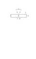
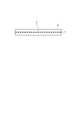
図2に示すように、板状の加工対象物1には、加工対象物1に改質領域を形成するための予定ラインである改質領域形成ライン5が設定されている。改質領域形成ライン5は、直線状に延びた仮想線である。加工対象物1の内部に改質領域を形成する場合、図3に示すように、加工対象物1の内部に集光点Pを合わせた状態で、レーザ光Lを改質領域形成ライン5に沿って(すなわち、図2の矢印A方向に)相対的に移動させる。これにより、図4〜図6に示すように、改質領域7が改質領域形成ライン5に沿って加工対象物1の内部に形成される。 As shown in FIG. 2, a modified
なお、集光点Pとは、レーザ光Lが集光する箇所のことである。また、改質領域形成ライン5は、直線状に限らず曲線状であってもよいし、仮想線に限らず加工対象物1の表面3に実際に引かれた線であってもよい。また、改質領域7は、連続的に形成される場合もあるし、断続的に形成される場合もある。また、改質領域7は少なくとも加工対象物1の内部に形成されていればよい。また、改質領域7を起点に亀裂が形成される場合があり、亀裂及び改質領域7は、加工対象物1の外表面(表面、裏面、若しくは外周面)に露出していてもよい。 In addition, the condensing point P is a location where the laser light L is condensed. The modified
ちなみに、ここでは、レーザ光Lが、加工対象物1を透過すると共に加工対象物1の内部の集光点近傍にて特に吸収され、これにより、加工対象物1に改質領域7が形成される(すなわち、内部吸収型レーザ加工)。よって、加工対象物1の表面3ではレーザ光Lが殆ど吸収されないので、加工対象物1の表面3が溶融することはない。一般的に、表面3から溶融され除去されて穴や溝等の除去部が形成される(表面吸収型レーザ加工)場合、加工領域は表面3側から徐々に裏面側に進行する。 Incidentally, here, the laser beam L passes through the
ところで、本実施形態にて形成される改質領域は、密度、屈折率、機械的強度やその他の物理的特性が周囲とは異なる状態になった領域をいう。例えば、(1)溶融処理領域、(2)クラック領域、絶縁破壊領域、(3)屈折率変化領域等があり、これらが混在した領域もある。 By the way, the modified region formed in the present embodiment refers to a region in which density, refractive index, mechanical strength, and other physical characteristics are different from the surroundings. For example, there are (1) a melt treatment region, (2) a crack region, a dielectric breakdown region, and (3) a refractive index change region, and there are regions where these are mixed.
本実施形態での改質領域は、レーザ光の局所的な吸収や多光子吸収という現象により形成される。多光子吸収とは、材料の吸収のバンドギャップEGよりも光子のエネルギーhνが小さいと光学的に透明となるため、材料に吸収が生じる条件はhν>EGであるが、光学的に透明でも、レーザ光Lの強度を非常に大きくするとnhν>EGの条件(n=2,3,4,・・・)で材料に吸収が生じる現象をいう。多光子吸収による溶融処理領域の形成は、例えば、溶接学会全国大会講演概要第66集(2000年4月)の第72頁〜第73頁の「ピコ秒パルスレーザによるシリコンの加工特性評価」に記載されている。The modified region in the present embodiment is formed by a phenomenon of local absorption of laser light or multiphoton absorption. The multiphoton absorption, since the energy hv of photons than the band gap EG of absorption of the material is small becomes optically transparent, but a condition under which absorption occurs in the material is hv> EG, optically transparent But, when a very large intensity of the laser beam L nhν> ofE G condition (n = 2,3,4, ···) refers to a phenomenon in which absorption occurs in the material. The formation of the melt-processed region by multiphoton absorption is described in, for example, “Evaluation of processing characteristics of silicon by picosecond pulse laser” on pages 72 to 73 of the 66th Annual Meeting of the Japan Welding Society (April 2000). Have been described.
また、D.Du,X.Liu,G.Korn,J.Squier,and G.Mourou,”Laser Induced Breakdown by Impact Ionization in SiO2 with Pulse Widths from 7ns to 150fs”,Appl Phys Lett64(23),Jun.6,1994に記載されているようにパルス幅が数ピコ秒からフェムト秒の超短パルスレーザ光を利用することにより形成される改質領域を利用してもよい。Also, D. Du, X. Liu, G. Korn, J. Squier, and G. Mourou, “Laser Induced Breakdown by Impact Ionization in SiO2 with Pulse Widths from 7ns to 150fs”, Appl Phys Lett64 (23), Jun As described in .6, 1994, a modified region formed by using an ultrashort pulse laser beam having a pulse width of several picoseconds to femtoseconds may be used.
(1)改質領域が溶融処理領域を含む場合
加工対象物(例えばシリコンのような半導体材料)の内部に集光点を合わせて、集光点における電界強度が1×10⁸(W/cm2)以上で且つパルス幅が1μs以下の条件でレーザ光Lを照射する。これにより、集光点近傍にてレーザ光Lが吸収されて加工対象物の内部が局所的に加熱され、この加熱により加工対象物の内部に溶融処理領域が形成される。(1) When the modified region includes a melt processing region The focusing point is set inside the object to be processed (for example, a semiconductor material such as silicon), and the electric field strength at the focusing point is 1 × 10⁸ (W / cm2 ) Irradiation with the laser beam L is performed under the conditions of the above and the pulse width of 1 μs or less. As a result, the laser beam L is absorbed in the vicinity of the condensing point, and the inside of the processing object is locally heated, and a melting treatment region is formed inside the processing object by this heating.
溶融処理領域とは、一旦溶融後再固化した領域や、まさに溶融状態の領域や、溶融状態から再固化する状態の領域であり、相変化した領域や結晶構造が変化した領域ということもできる。また、溶融処理領域とは単結晶構造、非晶質構造、多結晶構造において、ある構造が別の構造に変化した領域ということもできる。つまり、例えば、単結晶構造から非晶質構造に変化した領域、単結晶構造から多結晶構造に変化した領域、単結晶構造から非晶質構造及び多結晶構造を含む構造に変化した領域を意味する。加工対象物がシリコン単結晶構造の場合、溶融処理領域は例えば非晶質シリコン構造である。 The melt treatment region is a region once solidified after being melted, a region in a molten state, a region in which the material is resolidified from a molten state, and can also be referred to as a phase-changed region or a region in which the crystal structure has changed. The melt treatment region can also be said to be a region in which one structure is changed to another structure in a single crystal structure, an amorphous structure, or a polycrystalline structure. In other words, for example, a region changed from a single crystal structure to an amorphous structure, a region changed from a single crystal structure to a polycrystalline structure, or a region changed from a single crystal structure to a structure including an amorphous structure and a polycrystalline structure. To do. When the object to be processed has a silicon single crystal structure, the melt processing region has, for example, an amorphous silicon structure.
図7は、レーザ光が照射されたシリコンウェハ(半導体基板)の一部における断面の写真を表した図である。図7に示すように、半導体基板11の内部に溶融処理領域13が形成されている。 FIG. 7 is a view showing a photograph of a cross section of a part of a silicon wafer (semiconductor substrate) irradiated with laser light. As shown in FIG. 7, a
入射するレーザ光の波長に対して透過性の材料の内部に溶融処理領域13が形成されたことを説明する。図8は、レーザ光の波長とシリコン基板の内部の透過率との関係を示す線図である。ただし、シリコン基板の表面側と裏面側それぞれの反射成分を除去し、内部のみの透過率を示している。シリコン基板の厚さtが50μm、100μm、200μm、500μm、1000μmの各々について上記関係を示した。 It will be described that the
例えば、Nd:YAGレーザの波長である1064nmにおいて、シリコン基板の厚さが500μm以下の場合、シリコン基板の内部ではレーザ光Lが80%以上透過することが分かる。図7に示す半導体基板11の厚さは350μmであるので、溶融処理領域13は半導体基板11の中心付近、つまり表面から175μmの部分に形成される。この場合の透過率は、厚さ200μmのシリコンウェハを参考にすると、90%以上なので、レーザ光Lが半導体基板11の内部で吸収されるのは僅かであり、殆どが透過する。しかし、1×10⁸(W/cm2)以上で且つパルス幅が1μs以下の条件でレーザ光Lをシリコンウェハ内部に集光することで集光点とその近傍で局所的にレーザ光が吸収され溶融処理領域13が半導体基板11の内部に形成される。For example, when the thickness of the silicon substrate is 500 μm or less at the wavelength of 1064 nm of the Nd: YAG laser, it can be seen that the laser light L is transmitted by 80% or more inside the silicon substrate. Since the thickness of the
なお、シリコンウェハには、溶融処理領域を起点として亀裂が発生する場合がある。また、溶融処理領域に亀裂が内包されて形成される場合があり、この場合には、その亀裂が、溶融処理領域においての全面に渡って形成されていたり、一部分のみや複数部分に形成されていたりすることがある。更に、この亀裂は、自然に成長する場合もあるし、シリコンウェハに力が印加されることにより成長する場合もある。溶融処理領域から亀裂が自然に成長する場合には、溶融処理領域が溶融している状態から成長する場合と、溶融処理領域が溶融している状態から再固化する際に成長する場合とのいずれもある。ただし、どちらの場合も溶融処理領域はシリコンウェハの内部に形成され、切断面においては、図7に示すように、内部に溶融処理領域が形成されている。 Note that cracks may occur in the silicon wafer starting from the melt processing region. In some cases, cracks are included in the melt treatment region. In this case, the cracks are formed over the entire surface in the melt treatment region, or are formed in only a part or a plurality of parts. Sometimes. Furthermore, the crack may grow naturally or may grow by applying a force to the silicon wafer. When the crack grows naturally from the melt-processed area, either the case where the melt-processed area grows from the melted state or the case where the melt-processed area grows when re-solidified from the melted state There is also. However, in both cases, the melt processing region is formed inside the silicon wafer, and the melt processing region is formed inside the cut surface as shown in FIG.
(2)改質領域がクラック領域を含む場合
加工対象物(例えばガラスやLiTaO3からなる圧電材料)の内部に集光点を合わせて、集光点における電界強度が1×10⁸(W/cm2)以上で且つパルス幅が1μs以下の条件でレーザ光Lを照射する。このパルス幅の大きさは、加工対象物の内部にレーザ光Lが吸収されてクラック領域が形成される条件である。これにより、加工対象物の内部には光学的損傷という現象が発生する。この光学的損傷により加工対象物の内部に熱ひずみが誘起され、これにより加工対象物の内部に、1つ又は複数のクラックを含むクラック領域が形成される。クラック領域は絶縁破壊領域とも言える。(2) When the modified region includes a crack region The focusing point is set inside a workpiece (for example, a piezoelectric material made of glass or LiTaO3 ), and the electric field strength at the focusing point is 1 × 10⁸ (W / The laser light L is irradiated under the conditions of cm2 ) or more and a pulse width of 1 μs or less. The magnitude of the pulse width is a condition that the laser beam L is absorbed inside the workpiece and a crack region is formed. As a result, a phenomenon called optical damage occurs inside the workpiece. This optical damage induces thermal strain inside the workpiece, thereby forming a crack region containing one or more cracks inside the workpiece. It can be said that the crack region is a dielectric breakdown region.
図9は電界強度とクラックの大きさとの関係の実験結果を示す線図である。横軸はピークパワー密度であり、レーザ光Lがパルスレーザ光なので電界強度はピークパワー密度で表される。縦軸は1パルスのレーザ光Lにより加工対象物の内部に形成されたクラック部分(クラックスポット)の大きさを示している。クラックスポットが集まりクラック領域となる。クラックスポットの大きさは、クラックスポットの形状のうち、最大の長さとなる部分の大きさである。グラフ中の黒丸で示すデータは集光用レンズ(C)の倍率が100倍、開口数(NA)が0.80の場合である。一方、グラフ中の白丸で示すデータは集光用レンズ(C)の倍率が50倍、開口数(NA)が0.55の場合である。ピークパワー密度が1011(W/cm2)程度から加工対象物の内部にクラックスポットが発生し、ピークパワー密度が大きくなるに従いクラックスポットも大きくなることが分かる。FIG. 9 is a diagram showing the experimental results of the relationship between the electric field strength and the crack size. The horizontal axis represents the peak power density. Since the laser beam L is a pulse laser beam, the electric field strength is represented by the peak power density. The vertical axis indicates the size of a crack portion (crack spot) formed inside the workpiece by one pulse of laser light L. Crack spots gather to form a crack region. The size of the crack spot is the size of the portion having the maximum length in the shape of the crack spot. Data indicated by black circles in the graph is for the case where the magnification of the condenser lens (C) is 100 times and the numerical aperture (NA) is 0.80. On the other hand, the data indicated by the white circles in the graph is when the magnification of the condenser lens (C) is 50 times and the numerical aperture (NA) is 0.55. From the peak power density of about 1011 (W / cm2 ), it can be seen that a crack spot is generated inside the workpiece, and the crack spot increases as the peak power density increases.
(3)改質領域が屈折率変化領域を含む場合
加工対象物(例えばガラス)の内部に集光点を合わせて、集光点における電界強度が1×10⁸(W/cm2)以上で且つパルス幅が1ns以下の条件でレーザ光Lを照射する。このように、パルス幅が極めて短い状態で加工対象物の内部にレーザ光Lが吸収されると、そのエネルギーが熱エネルギーに転化せず、加工対象物の内部にはイオン価数変化、結晶化又は分極配向等の永続的な構造変化が誘起され、屈折率変化領域が形成される。(3) When the modified region includes a refractive index changing region The focusing point is set inside the object to be processed (for example, glass), and the electric field strength at the focusing point is 1 × 10⁸ (W / cm2 ) or more. In addition, the laser beam L is irradiated under the condition that the pulse width is 1 ns or less. Thus, when the laser beam L is absorbed inside the object to be processed in a state where the pulse width is extremely short, the energy is not converted into thermal energy, and the ion valence change, crystallization occurs inside the object to be processed. Alternatively, a permanent structural change such as a polarization orientation is induced, and a refractive index change region is formed.
なお、改質領域とは、溶融処理領域、絶縁破壊領域、屈折率変化領域等やそれらが混在した領域を含めて、その材料において改質領域の密度が非改質領域の密度と比較して変化した領域であったり、格子欠陥が形成された領域であったりする。これらをまとめて高密転移領域と言うこともできる。 Note that the modified region includes the melt-processed region, the dielectric breakdown region, the refractive index change region, etc., and the mixed region thereof, and the density of the modified region in the material is compared with the density of the non-modified region. It may be a changed region or a region where lattice defects are formed. These can be collectively referred to as a high-density transition region.
また、溶融処理領域や屈折率変化領域、改質領域の密度が非改質領域の密度と比較して変化した領域、格子欠陥が形成された領域は、更にそれら領域の内部や改質領域と非改質領域との界面に亀裂(割れ、マイクロクラック)を内包している場合がある。内包される亀裂は改質領域の全面に渡る場合や一部分のみや複数部分に形成される場合がある。 In addition, the area where the density of the melt-processed area, the refractive index changing area, the modified area is changed compared to the density of the non-modified area, and the area where lattice defects are formed are further divided into these areas and the modified area. In some cases, cracks (cracks, microcracks) are included in the interface with the non-modified region. The included crack may be formed over the entire surface of the modified region, or may be formed in only a part or a plurality of parts.
ちなみに、加工対象物の結晶構造やその劈開性等を考慮して、改質領域を次のように形成することが好ましい。 Incidentally, it is preferable to form the modified region as follows in consideration of the crystal structure of the workpiece, its cleavage, and the like.
すなわち、シリコン等のダイヤモンド構造の単結晶半導体からなる基板の場合は、(111)面(第1劈開面)や(110)面(第2劈開面)に沿った方向に改質領域を形成するのが好ましい。また、GaAs等の閃亜鉛鉱型構造のIII−V族化合物半導体からなる基板の場合は、(110)面に沿った方向に改質領域を形成するのが好ましい。更に、サファイア(Al2O3)等の六方晶系の結晶構造を有する基板の場合は、(0001)面(C面)を主面として(1120)面(A面)或いは(1100)面(M面)に沿った方向に改質領域を形成するのが好ましい。That is, in the case of a substrate made of a single crystal semiconductor having a diamond structure such as silicon, the modified region is formed in a direction along the (111) plane (first cleavage plane) or the (110) plane (second cleavage plane). Is preferred. Further, in the case of a substrate made of a zinc-blende-type III-V group compound semiconductor such as GaAs, it is preferable to form the modified region in the direction along the (110) plane. Furthermore, in the case of a substrate having a hexagonal crystal structure such as sapphire (Al2 O3 ), the (1120) plane (A plane) or (1100) plane ( It is preferable to form the modified region in a direction along the (M plane).
また、上述した改質領域を形成すべき方向(例えば、単結晶シリコン基板における(111)面に沿った方向)、或いは改質領域を形成すべき方向に直交する方向に沿って基板にオリエンテーションフラットを形成すれば、そのオリエンテーションフラットを基準とすることで、改質領域を容易且つ正確に基板に形成することが可能になる。 In addition, the orientation flat on the substrate along the direction in which the modified region is to be formed (for example, the direction along the (111) plane in the single crystal silicon substrate) or the direction perpendicular to the direction in which the modified region is to be formed. If this is formed, the modified region can be easily and accurately formed on the substrate by using the orientation flat as a reference.
次に、本発明の第1実施形態に係る加工対象物研削方法について説明する。 Next, the workpiece grinding method according to the first embodiment of the present invention will be described.
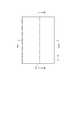
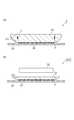
本実施形態の加工対象物研削方法は、例えば厚さが15μm〜25μm(所定の厚さ:以下、「最終研削厚さ」という)の極薄の半導体基板を形成するために加工対象物を研削するものである。図10に示すように、研削加工の対象となる加工対象物1は、例えばシリコンからなる円板状を呈している。ここでは、加工対象物1は、円筒状のシリコンインゴットを輪切り状に切断して形成されている。この加工対象物1は、その外縁Eから所定の距離内側に、改質領域形成ライン5が設定されている。なお、加工対象物1では、説明の便宜上オリエンテーションフラットを省略する。また、ここでの「研削」とは、砥石、刃物、エッチング液等で機械的、化学的、電気化学的に表面を削って滑らかにすることを意味し、また、研磨と同義である。 The processing object grinding method of this embodiment grinds a processing object in order to form an ultra-thin semiconductor substrate having a thickness of, for example, 15 μm to 25 μm (predetermined thickness: hereinafter referred to as “final grinding thickness”). To do. As shown in FIG. 10, the
この改質領域形成ライン5は、加工対象物1の外縁Eに沿った円環状を呈している。改質領域形成ライン5は、図12(a)に示すように、加工対象物1において外縁部25と該外縁部25の内側の有効領域26との境界に設定されている。外縁部25は、加工対象物1における曲面状に突出する側面を含んで構成された部分である。この外縁部25は、側方視において断面が弓形状を呈しており、その厚さが外側に行くに従って薄くなっている。なお、外縁部25は、側方視において断面が半弓形状や矩形状でもよく、また、その厚さが外側に行くに従って薄くなるストレートなテーパ状の場合もある。 The modified
有効領域26は、結晶成長により形成された半導体動作層、フォトダイオード等の受光素子、レーザダイオード等の発光素子、又は回路として形成された回路素子等の機能素子22を形成するための領域である。 The
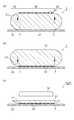
以上に説明した加工対象物1に研削加工を施す場合、まず、図11(a)に示すように、加工対象物1の裏面(主面)21にテープ31を貼り付けて保持し、この加工対象物1を、表面3が上方に位置するようにステージ(不図示)上に載置する。ここでのテープ31としては、BG(BackGrind)テープが用いられている。ちなみに、保持治具や保持基板で加工対象物1を保持してステージ上に載置する場合もある。 When grinding the
この状態で、加工対象物1の内部に集光点を合わせて加工対象物1の表面3側からレーザ光Lを照射しながら、レーザ光Lに対しステージをθ方向(図中の矢印R方向)に相対回転させる。これにより、図11(b)に示すように、外周縁の改質領域形成ライン5(図10参照)に沿って、加工対象物1の内部に改質領域7を形成し、改質領域7の上端部及び下端部から、厚さ方向に沿って延びる亀裂(割れ)C1を生じさせる。なお、この改質領域7には、その内部に亀裂が含まれてもよい。 In this state, the stage is moved toward the laser light L in the θ direction (in the direction of arrow R in the figure) while irradiating the laser light L from the
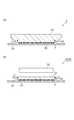
続いて、図12(a)に示すように、加工対象物1の表面3における有効領域26に、複数の機能素子22をマトリックス状に配設されるように形成した後、図12(b)に示すように、加工対象物1を上下反転して裏面21を上方に位置させる。そして、図12(c)に示すように、研削砥石32(グラインダー)で加工対象物1の裏面21を研削し、加工対象物1を最終研削厚さに薄化する。ここで、研削後の加工対象物1aでは、亀裂C1のみが残存しており、この亀裂C1が裏面21に露出している。つまり、裏面21にハーフカット亀裂C1が露出した状態となっている。 Subsequently, as shown in FIG. 12 (a), a plurality of
加工対象物1を薄化した後には、隣り合う機能素子22間を通るような格子状に設定された切断予定ラインに沿って、加工対象物1を切断するための切断起点領域が形成される。ここでは、切断起点領域として、加工対象物に集光点を合わせてレーザ光を照射し、改質領域7と同様な切断用改質領域を形成している。切断起点領域は、レーザアブレーション、スクライブ若しくはブレードダイシング等で形成された溝等でもよい。そして、加工対象物1がエキスパンドテープに張り替えられ、このエキスパンドテープが拡張されることで、切断起点領域を起点として加工対象物1が切断予定ラインに沿って分断(切断)される。ちなみに、加工対象物1の研削中、研削後又はエキスパンドテープ拡張時において、改質領域7を起点として改質領域形成ライン5(図10参照)に沿って加工対象物1が切断されてもよい。 After thinning the
ところで、従来、加工対象物1を研削して加工対象物1を薄化した場合、厚さが特に薄い外縁部25でチッピングや亀裂が生じ、亀裂が内側に伸展することがある。また、加工対象物1の研削中に、研削のために加工対象物1に加えられる力によって外縁部25でチッピングや亀裂が生じ、亀裂が内側に伸展することがある。つまり、加工対象物1の研削に起因して外縁部25で生じた割れが、有効領域26に向かって内側に伸展するおそれがある。 Incidentally, conventionally, when the
この点、本実施形態の加工対象物研削方法では、加工対象物1の外縁Eから所定の距離内側に設定された改質領域形成ライン5に沿って、加工対象物1に改質領域7を形成している。これにより、改質領域7又は改質領域7から延びる割れC1によって、外縁部25で生じた割れが有効領域26に向かって内側に伸展するのを抑制ひいては遮断することができ、加工対象物を確実に研削することができる。研削後の加工対象物1aの厚さが極薄の本実施形態では、外縁部25にチッピング(欠け)が特に生じ易いことから、かかる効果は顕著となる。 In this regard, in the workpiece grinding method of the present embodiment, the modified
図13(a)は、本実施形態の加工対象物研削方法による研削後の加工対象物における裏面側を示す平面図、図13(b)は、図13(a)のb−b線に沿う断面拡大図である。図13に示すように、加工対象物1aの外縁部25では、外縁部25にチッピング27が生じている。また、チッピング27及び外縁部25からは亀裂28が延びている。ここで、亀裂28は、上方視において亀裂C1が延在する円周方向に延び易くなっていることがわかる。また、亀裂28の加工対象物1の内側への進展が、亀裂C1で留まっているのがわかる。つまり、改質領域7及び改質領域7から延びた亀裂C1にあっては、亀裂28を内側に伸展させないストッパとして機能し、亀裂28が外縁部25から有効領域26へ延びるのを防ぐ予防線となっている。 Fig.13 (a) is a top view which shows the back surface side in the workpiece after grinding by the workpiece grinding method of this embodiment, FIG.13 (b) follows the bb line | wire of Fig.13 (a). It is a cross-sectional enlarged view. As shown in FIG. 13, a chipping 27 is generated at the
また、本実施形態では、上述したように、加工対象物1の研削が、改質領域7を形成した後に実施されている。これにより、加工対象物1の研削中にその外縁部25で亀裂28が発生したとしても、改質領域7又は改質領域7から延びる亀裂C1によって、亀裂28が内側に伸展するのを抑制することができる。 In the present embodiment, as described above, the grinding of the
また、本実施形態では、上述したように、研削後の加工対象物1aに亀裂C1のみが残存している。すなわち、改質領域7から延びる亀裂C1のみが研削後の加工対象物1aに残存するように、加工対象物1に改質領域7が形成されている。この場合、切削後の加工対象物1aには改質領域7が残存しないことから、発塵を低減することができる。 Moreover, in this embodiment, as above-mentioned, only the crack C1 remains in the
また、本実施形態では、上述したように、加工対象物1において外縁部25と有効領域26との境界に形成されている。ここで、加工対象物1においては、外縁部25の厚さが有効領域26の厚さよりも薄くなっていることから、外縁部25から亀裂が生じ易いため、外縁部25と有効領域26との境界に改質領域7を形成することで、亀裂が内側に伸展するのを確実に抑制することができる。また、外縁部25と有効領域26との境界の内側に改質領域7を形成してもよく、この場合には、上記と同様に亀裂が内側に伸展するのを確実に抑制することができる。さらに、外縁部25と有効領域26との境界の外側に改質領域7を形成してもよく、この場合には、有効領域を十分に活用することができる。 In the present embodiment, as described above, the
ちなみに、加工対象物1に改質領域7を形成した後に、その表面3に機能素子22を形成したが、表面3に機能素子22を形成した後に改質領域7を形成してもよく、改質領域7の形成と機能素子22の形成とは順不同である。これについては、以下の実施形態においても同様である。 Incidentally, after forming the modified
次に、本発明の第2実施形態に係る加工対象物研削方法について説明する。なお、本実施形態の説明においては、上記第1実施形態と異なる点を主に説明する。 Next, a workpiece grinding method according to a second embodiment of the present invention will be described. In the description of the present embodiment, differences from the first embodiment will be mainly described.
本実施形態の加工対象物研削方法では、図14(a)に示すように、改質領域7の上端部及び下端部から厚さ方向に沿って延びる亀裂C2を生じさせた加工対象物1を、裏面21が上方に位置するように配置する。そして、図14(b)に示すように、研削砥石32で加工対象物1の裏面21を研削し、加工対象物1を最終研削厚さに薄化する。ここで、研削後の加工対象物1bでは、改質領域7が残存しており、改質領域7及びこの改質領域7から延びる亀裂C2が、表面3及び裏面21に露出しない状態となっている。 In the workpiece grinding method of the present embodiment, as shown in FIG. 14A, the
本実施形態においても、上記実施形態と同様な効果、すなわち、加工対象物1を確実に研削するという効果等を奏する。また、本実施形態では、研削後の加工対象物1bにおいて改質領域7が表面3及び裏面21に露出しないため、発塵を低減することができる。 Also in this embodiment, the same effects as the above-described embodiment, that is, the effect of reliably grinding the
次に、本発明の第3実施形態に係る加工対象物研削方法について説明する。なお、本実施形態の説明においては、上記第1実施形態と異なる点を主に説明する。 Next, a workpiece grinding method according to a third embodiment of the present invention will be described. In the description of the present embodiment, differences from the first embodiment will be mainly described.
本実施形態の加工対象物研削方法では、図15(a)に示すように、加工対象物1の表面3に複数の機能素子22を形成してテープ31を貼り付け、この加工対象物1を裏面21が上方に位置するようにステージ上に載置する。そして、図15(b)に示すように、研削砥石32で加工対象物1の裏面21を研削し、最終研削厚さよりも厚い状態まで加工対象物1を薄化する。ここでは、加工対象物1が略半分の厚さになるように薄化している。なお、この際の研削後の裏面21の表面粗さは、後に照射するレーザ光Lを透過させ得る粗さ程度にまで仕上がっていることが好ましい。 In the processing object grinding method of this embodiment, as shown to Fig.15 (a), the some
この状態で、図15(c)に示すように、加工対象物1の内部に集光点を合わせて加工対象物1の裏面21側からレーザ光Lを照射しながら、ステージをθ方向(図中の矢印R方向)に相対回転させる。これにより、図16(a)に示すように、改質領域形成ライン5に沿って加工対象物1の内部に改質領域7を形成し、この改質領域7の上端部及び下端部から、厚さ方向に沿って延びる亀裂C3生じさせる。 In this state, as shown in FIG. 15 (c), the stage is moved in the θ direction while the laser beam L is irradiated from the
そして、図16(b)に示すように、研削砥石32で加工対象物1の裏面21を再び研削し、加工対象物1を最終研削厚さに薄化する。ここで、研削後の加工対象物1cでは、亀裂C3のみが残存しており、この亀裂C3が表面3及び裏面21に露出している。つまり、表面3及び裏面21にハーフカット亀裂C3が露出した状態となっている。 And as shown in FIG.16 (b), the
本実施形態においても、上記実施形態と同様な効果、すなわち、加工対象物1を確実に研削するという効果等を奏する。また、本実施形態では、上述したように、表面3及び裏面21の双方に亀裂C3が露出しているため、加工対象物1の外縁部25で生じた亀裂が内側に伸展するのを一層抑制することができる。 Also in this embodiment, the same effects as the above-described embodiment, that is, the effect of reliably grinding the
次に、本発明の第4実施形態に係る加工対象物研削方法について説明する。なお、本実施形態の説明においては、上記第3実施形態と異なる点を主に説明する。 Next, a workpiece grinding method according to a fourth embodiment of the present invention will be described. In the description of the present embodiment, differences from the third embodiment will be mainly described.
本実施形態の加工対象物研削方法では、研削砥石32で加工対象物1の裏面21を研削し、最終研削厚さよりも厚い状態まで加工対象物1を薄化した後、図17(a)に示すように、改質領域形成ライン5に沿って、加工対象物1の内部に改質領域7を形成し、この改質領域7の上端部及び下端部から、厚さ方向に沿って延びる亀裂C4を生じさせる。 In the processing object grinding method of this embodiment, after grinding the
そして、図17(b)に示すように、研削砥石32で加工対象物1の裏面21を研削し、加工対象物1を最終研削厚さに薄化する。ここで、研削後の加工対象物1dでは、改質領域7が残存しており、改質領域7及び改質領域7から延びる亀裂C2が、表面3及び裏面21に露出しない状態となっている。 And as shown in FIG.17 (b), the
本実施形態においても、上記実施形態と同様な効果、すなわち、加工対象物1を確実に研削するという効果等を奏する。また、本実施形態では、研削後の加工対象物1dにおいて改質領域7が表面3及び裏面21に露出しないため、発塵を低減することができる。 Also in this embodiment, the same effects as the above-described embodiment, that is, the effect of reliably grinding the
次に、本発明の第5実施形態に係る加工対象物研削方法について説明する。なお、本実施形態の説明においては、上記第3実施形態と異なる点を主に説明する。 Next, a workpiece grinding method according to a fifth embodiment of the present invention will be described. In the description of the present embodiment, differences from the third embodiment will be mainly described.
本実施形態の加工対象物研削方法では、研削砥石32で加工対象物1の裏面21を研削し、最終研削厚さよりも厚い状態まで加工対象物1を薄化した後、図18(a)に示すように、改質領域形成ライン5に沿って、加工対象物1の内部に改質領域7を形成し、この改質領域7の上端部及び下端部から、厚さ方向に沿って延びる亀裂C5を生じさせる。 In the processing object grinding method of this embodiment, after grinding the
そして、図18(b)に示すように、研削砥石32で加工対象物1の裏面21を研削し、加工対象物1を最終研削厚さに薄化する。ここで、研削後の加工対象物1eでは、亀裂C5のみが残存しており、この亀裂C5が裏面21に露出している。つまり、裏面21にハーフカット亀裂C5が露出した状態となっている。 Then, as shown in FIG. 18B, the
本実施形態においても、上記実施形態と同様な効果、すなわち、加工対象物1を確実に研削するという効果等を奏する。 Also in this embodiment, the same effects as the above-described embodiment, that is, the effect of reliably grinding the
本発明は、上記実施形態に限定されるものではない。例えば、上記実施形態では、加工対象物1にテープ31を貼り付けたが、加工対象物1を保持し得るテープ以外の保持具でもよいし、図19に示すように、環状のダイシングフレーム33で保持されたダイシングテープ34を貼り付けてもよい。この場合、加工対象物1を分断する際に拡張するエキスパンドテープとして、ダイシングテープ34を利用することができる。 The present invention is not limited to the above embodiment. For example, in the said embodiment, although the
また、上記実施形態では、加工対象物1に改質領域7を形成した後に加工対象物1を最終研削厚さに研削したが、これとは逆に、加工対象物1を最終研削厚さに研削した後に加工対象物1に改質領域7を形成してもよい。ただし、研削前に改質領域7を形成する方が、研削後のハンドリング等の際に外縁部25から発生する亀裂28をストップさせることができるため、より望ましい。 Moreover, in the said embodiment, after forming the modification | reformation area |
また、上記実施形態では、改質領域7は亀裂C1〜C5を含んでいるが、改質領域(溶融処理領域)のみでもよい。切断予定ラインに沿って加工対象物1の内部に切断の起点となる改質領域を形成し加工対象物1をチップ状に切断するという方法(=ステルスダイシング方式)や、レーザスクライブのように溝を形成し加工対象物1に応力を印加してチップ状に切断するという方法においては、亀裂が存在している方が、ダイシングテープを拡張する際に加工対象物1に応力を加え易くなり加工対象物1の切断が容易になると共に、外縁部25の切断も容易となる。 Moreover, in the said embodiment, although the modification | reformation area |
また、上記実施形態は、半導体材料からなる加工対象物1に溶融処理領域を含む改質領域7を形成したが、ガラスや圧電材料等、他の材料からなる加工対象物の内部に、クラック領域や屈折率変化領域等、他の改質領域を形成してもよい。また、上記実施形態での亀裂は、切れ目及び裂け目等の割れであってもよい。 Moreover, although the said embodiment formed the modification | reformation area |
なお、本発明において、外縁(外周円)Eに沿って改質領域7が形成された研削済みの加工対象物1には、上述したステルスダイシング方式やスクライビングによる切断方式、レーザによる完全切断やブレードダイシング等の切断方法が利用できる。 In the present invention, the
1,1a,1b,1c,1d,1e…加工対象物、5…改質領域形成ライン、7…改質領域、21…裏面(主面)、C1〜C5…改質領域から延びる亀裂、E…外縁、L…レーザ光、P…集光点。
1, 1a, 1b, 1c, 1d, 1e ... workpiece, 5 ... modified region forming line, 7 ... modified region, 21 ... back surface (main surface), C1 to C5 ... cracks extending from the modified region, E ... outer edge, L ... laser beam, P ... condensing point.
Claims (2)
Translated fromJapanese前記加工対象物の内部に集光点を合わせてレーザ光を照射することにより、前記加工対象物の外縁から所定の距離内側に前記外縁に沿って設定された改質領域形成ラインに沿って、前記加工対象物に改質領域を形成する工程と、
前記改質領域を形成した後に、前記加工対象物の一方の主面を保持手段で保持した状態で、前記加工対象物の他方の主面を研削し、前記改質領域を残存させずに、前記改質領域から延びる割れを残存させて、前記割れを少なくとも前記加工対象物の前記他方の主面に露出させる工程と、を含むことを特徴とする加工対象物研削方法。A workpiece grinding method for grinding a plate-like workpiece to a predetermined thickness,
Along the modified region forming line set along the outer edge within a predetermined distance from the outer edge of the workpiece by irradiating a laser beam with a focusing point inside the workpiece. Forming a modified region in the workpiece;
After forming the modified region, withthe one main surface ofthe workpiece to be held by a holding means, grinding the other main surface of the workpiece, without leaving the modified region, wherein by residual cracks extending from the modified region, the object grinding method which comprises the the steps of exposing tothe other main surface of the crack at least the workpiece.
前記加工対象物の内部に集光点を合わせてレーザ光を照射することにより、前記加工対象物の外縁から所定の距離内側に前記外縁に沿って設定された改質領域形成ラインに沿って、前記加工対象物に改質領域を形成する工程と、
前記改質領域を形成した後に、前記加工対象物の一方の主面を保持手段で保持した状態で、前記加工対象物の他方の主面を研削し、前記改質領域、及び前記改質領域から延びる割れを残存させて、前記割れを前記加工対象物の前記一方の主面及び前記他方の主面に露出させない工程と、を含むことを特徴とする加工対象物研削方法。A workpiece grinding method for grinding a plate-like workpiece to a predetermined thickness,
Along the modified region forming line set along the outer edge within a predetermined distance from the outer edge of the workpiece by irradiating a laser beam with a focusing point inside the workpiece. Forming a modified region in the workpiece;
After forming the modified region,the other principal surface of the workpiece is ground in a state where the one principal surface of the workpiece is held by a holding unit, and the modified region and the modified region It is left cracks extending from the workpiece grinding method which comprises the the steps of not exposedthe one principal surface andthe other main surface of the crack the workpiece.
Priority Applications (7)
| Application Number | Priority Date | Filing Date | Title |
|---|---|---|---|
| JP2007311643AJP5134928B2 (en) | 2007-11-30 | 2007-11-30 | Workpiece grinding method |
| CN2008801182847ACN101878092B (en) | 2007-11-30 | 2008-11-18 | Object Grinding Method |
| US12/744,714US8523636B2 (en) | 2007-11-30 | 2008-11-18 | Working object grinding method |
| KR1020107010361AKR101607341B1 (en) | 2007-11-30 | 2008-11-18 | Working object grinding method |
| PCT/JP2008/070947WO2009069509A1 (en) | 2007-11-30 | 2008-11-18 | Working object grinding method |
| EP08853744.4AEP2236243A4 (en) | 2007-11-30 | 2008-11-18 | Working object grinding method |
| TW97145750ATWI471195B (en) | 2007-11-30 | 2008-11-26 | Processing object grinding method |
Applications Claiming Priority (1)
| Application Number | Priority Date | Filing Date | Title |
|---|---|---|---|
| JP2007311643AJP5134928B2 (en) | 2007-11-30 | 2007-11-30 | Workpiece grinding method |
Publications (2)
| Publication Number | Publication Date |
|---|---|
| JP2009131942A JP2009131942A (en) | 2009-06-18 |
| JP5134928B2true JP5134928B2 (en) | 2013-01-30 |
Family
ID=40678411
Family Applications (1)
| Application Number | Title | Priority Date | Filing Date |
|---|---|---|---|
| JP2007311643AActiveJP5134928B2 (en) | 2007-11-30 | 2007-11-30 | Workpiece grinding method |
Country Status (7)
| Country | Link |
|---|---|
| US (1) | US8523636B2 (en) |
| EP (1) | EP2236243A4 (en) |
| JP (1) | JP5134928B2 (en) |
| KR (1) | KR101607341B1 (en) |
| CN (1) | CN101878092B (en) |
| TW (1) | TWI471195B (en) |
| WO (1) | WO2009069509A1 (en) |
Families Citing this family (93)
| Publication number | Priority date | Publication date | Assignee | Title |
|---|---|---|---|---|
| JP4659300B2 (en) | 2000-09-13 | 2011-03-30 | 浜松ホトニクス株式会社 | Laser processing method and semiconductor chip manufacturing method |
| TWI326626B (en) | 2002-03-12 | 2010-07-01 | Hamamatsu Photonics Kk | Laser processing method |
| EP2400539B1 (en) | 2002-03-12 | 2017-07-26 | Hamamatsu Photonics K.K. | Substrate dividing method |
| WO2003076119A1 (en) | 2002-03-12 | 2003-09-18 | Hamamatsu Photonics K.K. | Method of cutting processed object |
| TWI520269B (en) | 2002-12-03 | 2016-02-01 | Hamamatsu Photonics Kk | Cutting method of semiconductor substrate |
| FR2852250B1 (en) | 2003-03-11 | 2009-07-24 | Jean Luc Jouvin | PROTECTIVE SHEATH FOR CANNULA, AN INJECTION KIT COMPRISING SUCH ANKLE AND NEEDLE EQUIPPED WITH SUCH ANKLE |
| DE60315515T2 (en) | 2003-03-12 | 2007-12-13 | Hamamatsu Photonics K.K., Hamamatsu | LASER PROCESSING PROCEDURES |
| CN101862907B (en)* | 2003-07-18 | 2014-01-22 | 浜松光子学株式会社 | Laser beam machining method, laser beam machining apparatus, and laser machined product |
| JP4563097B2 (en) | 2003-09-10 | 2010-10-13 | 浜松ホトニクス株式会社 | Semiconductor substrate cutting method |
| JP4509578B2 (en) | 2004-01-09 | 2010-07-21 | 浜松ホトニクス株式会社 | Laser processing method and laser processing apparatus |
| JP4598407B2 (en) | 2004-01-09 | 2010-12-15 | 浜松ホトニクス株式会社 | Laser processing method and laser processing apparatus |
| JP4601965B2 (en) | 2004-01-09 | 2010-12-22 | 浜松ホトニクス株式会社 | Laser processing method and laser processing apparatus |
| EP1742253B1 (en) | 2004-03-30 | 2012-05-09 | Hamamatsu Photonics K.K. | Laser processing method |
| KR101109860B1 (en)* | 2004-08-06 | 2012-02-21 | 하마마츠 포토닉스 가부시키가이샤 | Laser processing method, cutting method for work and semiconductor device |
| JP4762653B2 (en)* | 2005-09-16 | 2011-08-31 | 浜松ホトニクス株式会社 | Laser processing method and laser processing apparatus |
| JP4907965B2 (en)* | 2005-11-25 | 2012-04-04 | 浜松ホトニクス株式会社 | Laser processing method |
| JP4804911B2 (en)* | 2005-12-22 | 2011-11-02 | 浜松ホトニクス株式会社 | Laser processing equipment |
| JP4907984B2 (en) | 2005-12-27 | 2012-04-04 | 浜松ホトニクス株式会社 | Laser processing method and semiconductor chip |
| JP5183892B2 (en) | 2006-07-03 | 2013-04-17 | 浜松ホトニクス株式会社 | Laser processing method |
| EP1875983B1 (en) | 2006-07-03 | 2013-09-11 | Hamamatsu Photonics K.K. | Laser processing method and chip |
| CN101516566B (en)* | 2006-09-19 | 2012-05-09 | 浜松光子学株式会社 | Laser processing method and laser processing apparatus |
| JP4954653B2 (en) | 2006-09-19 | 2012-06-20 | 浜松ホトニクス株式会社 | Laser processing method |
| JP5101073B2 (en)* | 2006-10-02 | 2012-12-19 | 浜松ホトニクス株式会社 | Laser processing equipment |
| JP5132911B2 (en)* | 2006-10-03 | 2013-01-30 | 浜松ホトニクス株式会社 | Laser processing method |
| JP4964554B2 (en)* | 2006-10-03 | 2012-07-04 | 浜松ホトニクス株式会社 | Laser processing method |
| WO2008041604A1 (en)* | 2006-10-04 | 2008-04-10 | Hamamatsu Photonics K.K. | Laser processing method |
| JP5336054B2 (en)* | 2007-07-18 | 2013-11-06 | 浜松ホトニクス株式会社 | Processing information supply system provided with processing information supply device |
| JP5449665B2 (en)* | 2007-10-30 | 2014-03-19 | 浜松ホトニクス株式会社 | Laser processing method |
| JP5054496B2 (en)* | 2007-11-30 | 2012-10-24 | 浜松ホトニクス株式会社 | Processing object cutting method |
| JP5692969B2 (en) | 2008-09-01 | 2015-04-01 | 浜松ホトニクス株式会社 | Aberration correction method, laser processing method using this aberration correction method, laser irradiation method using this aberration correction method, aberration correction apparatus, and aberration correction program |
| JP5517284B2 (en) | 2008-09-03 | 2014-06-11 | 西川ゴム工業株式会社 | Thermostable double-strand specific nuclease |
| JP5254761B2 (en) | 2008-11-28 | 2013-08-07 | 浜松ホトニクス株式会社 | Laser processing equipment |
| JP5241527B2 (en) | 2009-01-09 | 2013-07-17 | 浜松ホトニクス株式会社 | Laser processing equipment |
| JP5241525B2 (en) | 2009-01-09 | 2013-07-17 | 浜松ホトニクス株式会社 | Laser processing equipment |
| KR101757937B1 (en) | 2009-02-09 | 2017-07-13 | 하마마츠 포토닉스 가부시키가이샤 | Workpiece cutting method |
| JP5639997B2 (en) | 2009-04-07 | 2014-12-10 | 浜松ホトニクス株式会社 | Laser processing equipment |
| JP5491761B2 (en) | 2009-04-20 | 2014-05-14 | 浜松ホトニクス株式会社 | Laser processing equipment |
| JP5452247B2 (en)* | 2010-01-21 | 2014-03-26 | 東芝機械株式会社 | Laser dicing equipment |
| JP5817116B2 (en) | 2010-02-03 | 2015-11-18 | 東洋製罐株式会社 | Diamond surface polishing method |
| DE102010009015A1 (en)* | 2010-02-24 | 2011-08-25 | OSRAM Opto Semiconductors GmbH, 93055 | Method for producing a plurality of optoelectronic semiconductor chips |
| JP2011200926A (en)* | 2010-03-26 | 2011-10-13 | Mitsuboshi Diamond Industrial Co Ltd | Laser beam machining method and brittle material substrate |
| JP5981094B2 (en) | 2010-06-24 | 2016-08-31 | 東芝機械株式会社 | Dicing method |
| US8722516B2 (en) | 2010-09-28 | 2014-05-13 | Hamamatsu Photonics K.K. | Laser processing method and method for manufacturing light-emitting device |
| JP5645593B2 (en)* | 2010-10-21 | 2014-12-24 | 株式会社ディスコ | Wafer division method |
| JP5841738B2 (en) | 2011-04-05 | 2016-01-13 | 株式会社ディスコ | Wafer grinding method |
| JP5140198B1 (en) | 2011-07-27 | 2013-02-06 | 東芝機械株式会社 | Laser dicing method |
| JP2013055160A (en)* | 2011-09-01 | 2013-03-21 | Canon Inc | Light transmissive member, optical device, and manufacturing method of them |
| JP5916336B2 (en)* | 2011-10-17 | 2016-05-11 | 株式会社ディスコ | Wafer grinding method |
| JP2014053510A (en)* | 2012-09-07 | 2014-03-20 | Toshiba Corp | End face processing method and end face processing device |
| CN103811602A (en)* | 2012-11-09 | 2014-05-21 | 上海蓝光科技有限公司 | GaN-base LED chip making method |
| US9425109B2 (en)* | 2014-05-30 | 2016-08-23 | Taiwan Semiconductor Manufacturing Co., Ltd. | Planarization method, method for polishing wafer, and CMP system |
| JP6360411B2 (en)* | 2014-10-09 | 2018-07-18 | 株式会社ディスコ | Wafer processing method |
| JP5900811B2 (en)* | 2015-08-28 | 2016-04-06 | 株式会社東京精密 | Semiconductor substrate cleaving method |
| JP6410152B2 (en)* | 2015-09-11 | 2018-10-24 | 東芝メモリ株式会社 | Manufacturing method of semiconductor device |
| JP6081005B2 (en)* | 2016-04-21 | 2017-02-15 | 株式会社東京精密 | Grinding / polishing apparatus and grinding / polishing method |
| JP6081006B2 (en)* | 2016-04-26 | 2017-02-15 | 株式会社東京精密 | Wafer cleaving method and wafer cleaving apparatus |
| JP6081008B2 (en)* | 2016-06-13 | 2017-02-15 | 株式会社東京精密 | Wafer processing apparatus and wafer processing method |
| JP2018006575A (en)* | 2016-07-01 | 2018-01-11 | 株式会社ディスコ | Method of processing laminated wafer |
| JP6908464B2 (en) | 2016-09-15 | 2021-07-28 | 株式会社荏原製作所 | Substrate processing method and substrate processing equipment |
| JP6327490B2 (en)* | 2016-11-14 | 2018-05-23 | 株式会社東京精密 | Wafer processing apparatus and wafer processing method |
| JP6935224B2 (en)* | 2017-04-25 | 2021-09-15 | 株式会社ディスコ | Wafer generation method |
| DE102017212858B4 (en)* | 2017-07-26 | 2024-08-29 | Disco Corporation | Method for processing a substrate |
| JP2019150925A (en)* | 2018-03-05 | 2019-09-12 | 株式会社ディスコ | Method for grinding work-piece |
| KR102719938B1 (en) | 2018-03-14 | 2024-10-23 | 도쿄엘렉트론가부시키가이샤 | Substrate processing system, substrate processing method and computer storage medium |
| JP2018142717A (en)* | 2018-04-20 | 2018-09-13 | 株式会社東京精密 | Wafer processing method and wafer processing system |
| JP6934563B2 (en) | 2018-04-27 | 2021-09-15 | 東京エレクトロン株式会社 | Board processing system and board processing method |
| WO2019208359A1 (en)* | 2018-04-27 | 2019-10-31 | 東京エレクトロン株式会社 | Substrate processing system and substrate processing method |
| JP7085426B2 (en)* | 2018-07-05 | 2022-06-16 | 株式会社ディスコ | Grinding method for workpieces |
| WO2020017599A1 (en) | 2018-07-19 | 2020-01-23 | 東京エレクトロン株式会社 | Substrate treatment system and substrate treatment method |
| JP7193956B2 (en)* | 2018-09-03 | 2022-12-21 | 株式会社ディスコ | Wafer processing method |
| JP2020057709A (en)* | 2018-10-03 | 2020-04-09 | 株式会社ディスコ | Wafer processing method |
| JP6703073B2 (en)* | 2018-10-03 | 2020-06-03 | 株式会社東京精密 | Wafer processing method and wafer processing system |
| JP6703072B2 (en)* | 2018-10-03 | 2020-06-03 | 株式会社東京精密 | Wafer processing method and wafer processing system |
| US10589445B1 (en)* | 2018-10-29 | 2020-03-17 | Semivation, LLC | Method of cleaving a single crystal substrate parallel to its active planar surface and method of using the cleaved daughter substrate |
| JP7460322B2 (en)* | 2018-11-27 | 2024-04-02 | 株式会社ディスコ | Wafer Processing Method |
| KR102745886B1 (en) | 2018-12-21 | 2024-12-23 | 도쿄엘렉트론가부시키가이샤 | Substrate processing device and substrate processing method |
| CN113195153B (en) | 2018-12-21 | 2023-04-07 | 东京毅力科创株式会社 | Substrate processing apparatus and substrate processing method |
| WO2020129734A1 (en) | 2018-12-21 | 2020-06-25 | 東京エレクトロン株式会社 | Substrate processing apparatus and substrate processing method |
| US11024501B2 (en) | 2018-12-29 | 2021-06-01 | Cree, Inc. | Carrier-assisted method for parting crystalline material along laser damage region |
| US10562130B1 (en) | 2018-12-29 | 2020-02-18 | Cree, Inc. | Laser-assisted method for parting crystalline material |
| US10576585B1 (en) | 2018-12-29 | 2020-03-03 | Cree, Inc. | Laser-assisted method for parting crystalline material |
| TWI816968B (en)* | 2019-01-23 | 2023-10-01 | 日商東京威力科創股份有限公司 | Substrate processing device and substrate processing method |
| TWI809251B (en)* | 2019-03-08 | 2023-07-21 | 日商東京威力科創股份有限公司 | Substrate processing device and substrate processing method |
| CN113518686B (en) | 2019-03-28 | 2023-05-26 | 东京毅力科创株式会社 | Processing apparatus and processing method |
| US10611052B1 (en) | 2019-05-17 | 2020-04-07 | Cree, Inc. | Silicon carbide wafers with relaxed positive bow and related methods |
| JP7286464B2 (en)* | 2019-08-02 | 2023-06-05 | 株式会社ディスコ | Laser processing equipment |
| TWI855139B (en) | 2019-10-28 | 2024-09-11 | 日商東京威力科創股份有限公司 | Substrate processing method and substrate processing system |
| JP7436187B2 (en)* | 2019-11-25 | 2024-02-21 | 株式会社ディスコ | Wafer processing method |
| JP7436219B2 (en)* | 2020-01-27 | 2024-02-21 | 浜松ホトニクス株式会社 | Laser processing equipment and laser processing method |
| GB2592905A (en)* | 2020-01-31 | 2021-09-15 | Smart Photonics Holding B V | Processing a wafer of a semiconductor material |
| JP7401372B2 (en)* | 2020-03-26 | 2023-12-19 | 株式会社ディスコ | Wafer processing method |
| JP7515292B2 (en)* | 2020-04-28 | 2024-07-12 | 株式会社ディスコ | Chip manufacturing method and edge trimming device |
| CN119217157B (en)* | 2024-12-04 | 2025-05-16 | 江苏矽腾半导体材料有限公司 | A method for grinding single crystal silicon |
Family Cites Families (63)
| Publication number | Priority date | Publication date | Assignee | Title |
|---|---|---|---|---|
| US4546231A (en)* | 1983-11-14 | 1985-10-08 | Group Ii Manufacturing Ltd. | Creation of a parting zone in a crystal structure |
| JPH0775818B2 (en) | 1986-08-08 | 1995-08-16 | 株式会社東芝 | Diamond member processing method |
| KR0171947B1 (en) | 1995-12-08 | 1999-03-20 | 김주용 | Exposure method for manufacturing semiconductor device and exposure device using same |
| JP4659300B2 (en)* | 2000-09-13 | 2011-03-30 | 浜松ホトニクス株式会社 | Laser processing method and semiconductor chip manufacturing method |
| CN1328009C (en)* | 2001-08-02 | 2007-07-25 | 株式会社Skc | Method for fabricating chemical mechanical polishing pad using laser |
| JP4509573B2 (en) | 2002-03-12 | 2010-07-21 | 浜松ホトニクス株式会社 | Semiconductor substrate, semiconductor chip, and semiconductor device manufacturing method |
| WO2003076119A1 (en)* | 2002-03-12 | 2003-09-18 | Hamamatsu Photonics K.K. | Method of cutting processed object |
| TWI326626B (en)* | 2002-03-12 | 2010-07-01 | Hamamatsu Photonics Kk | Laser processing method |
| EP2400539B1 (en)* | 2002-03-12 | 2017-07-26 | Hamamatsu Photonics K.K. | Substrate dividing method |
| JP2004111606A (en)* | 2002-09-18 | 2004-04-08 | Tokyo Seimitsu Co Ltd | Method of processing wafer |
| TWI520269B (en)* | 2002-12-03 | 2016-02-01 | Hamamatsu Photonics Kk | Cutting method of semiconductor substrate |
| EP1588793B1 (en)* | 2002-12-05 | 2012-03-21 | Hamamatsu Photonics K.K. | Laser processing devices |
| JP2004188422A (en)* | 2002-12-06 | 2004-07-08 | Hamamatsu Photonics Kk | Device and method for machining laser beam |
| JP4334864B2 (en)* | 2002-12-27 | 2009-09-30 | 日本電波工業株式会社 | Thin plate crystal wafer and method for manufacturing crystal resonator |
| FR2852250B1 (en)* | 2003-03-11 | 2009-07-24 | Jean Luc Jouvin | PROTECTIVE SHEATH FOR CANNULA, AN INJECTION KIT COMPRISING SUCH ANKLE AND NEEDLE EQUIPPED WITH SUCH ANKLE |
| DE60315515T2 (en)* | 2003-03-12 | 2007-12-13 | Hamamatsu Photonics K.K., Hamamatsu | LASER PROCESSING PROCEDURES |
| JP4494728B2 (en) | 2003-05-26 | 2010-06-30 | 株式会社ディスコ | Non-metallic substrate division method |
| CN101862907B (en)* | 2003-07-18 | 2014-01-22 | 浜松光子学株式会社 | Laser beam machining method, laser beam machining apparatus, and laser machined product |
| JP4563097B2 (en)* | 2003-09-10 | 2010-10-13 | 浜松ホトニクス株式会社 | Semiconductor substrate cutting method |
| JP2005086175A (en)* | 2003-09-11 | 2005-03-31 | Hamamatsu Photonics Kk | Method of manufacturing semiconductor thin film, semiconductor thin film, semiconductor thin-film chip, electron tube and light detector |
| JP4398686B2 (en)* | 2003-09-11 | 2010-01-13 | 株式会社ディスコ | Wafer processing method |
| EP1705764B1 (en)* | 2004-01-07 | 2012-11-14 | Hamamatsu Photonics K. K. | Semiconductor light-emitting device and its manufacturing method |
| JP4601965B2 (en)* | 2004-01-09 | 2010-12-22 | 浜松ホトニクス株式会社 | Laser processing method and laser processing apparatus |
| JP4509578B2 (en)* | 2004-01-09 | 2010-07-21 | 浜松ホトニクス株式会社 | Laser processing method and laser processing apparatus |
| JP4598407B2 (en)* | 2004-01-09 | 2010-12-15 | 浜松ホトニクス株式会社 | Laser processing method and laser processing apparatus |
| JP4943636B2 (en)* | 2004-03-25 | 2012-05-30 | エルピーダメモリ株式会社 | Semiconductor device and manufacturing method thereof |
| EP1742253B1 (en)* | 2004-03-30 | 2012-05-09 | Hamamatsu Photonics K.K. | Laser processing method |
| JP4536407B2 (en)* | 2004-03-30 | 2010-09-01 | 浜松ホトニクス株式会社 | Laser processing method and object to be processed |
| KR101336402B1 (en)* | 2004-03-30 | 2013-12-04 | 하마마츠 포토닉스 가부시키가이샤 | Laser processing method and semiconductor chip |
| JP4634089B2 (en)* | 2004-07-30 | 2011-02-16 | 浜松ホトニクス株式会社 | Laser processing method |
| KR101109860B1 (en)* | 2004-08-06 | 2012-02-21 | 하마마츠 포토닉스 가부시키가이샤 | Laser processing method, cutting method for work and semiconductor device |
| JP2006108532A (en) | 2004-10-08 | 2006-04-20 | Disco Abrasive Syst Ltd | Wafer grinding method |
| JP4754801B2 (en)* | 2004-10-13 | 2011-08-24 | 浜松ホトニクス株式会社 | Laser processing method |
| JP4917257B2 (en)* | 2004-11-12 | 2012-04-18 | 浜松ホトニクス株式会社 | Laser processing method |
| JP4781661B2 (en)* | 2004-11-12 | 2011-09-28 | 浜松ホトニクス株式会社 | Laser processing method |
| JP4198123B2 (en)* | 2005-03-22 | 2008-12-17 | 浜松ホトニクス株式会社 | Laser processing method |
| JP4776994B2 (en)* | 2005-07-04 | 2011-09-21 | 浜松ホトニクス株式会社 | Processing object cutting method |
| JP4749799B2 (en)* | 2005-08-12 | 2011-08-17 | 浜松ホトニクス株式会社 | Laser processing method |
| CN100399540C (en)* | 2005-08-30 | 2008-07-02 | 中美矽晶制品股份有限公司 | Method for manufacturing composite wafer structure |
| JP4762653B2 (en)* | 2005-09-16 | 2011-08-31 | 浜松ホトニクス株式会社 | Laser processing method and laser processing apparatus |
| JP2007096115A (en)* | 2005-09-29 | 2007-04-12 | Fujitsu Ltd | Manufacturing method of semiconductor device |
| JP4237745B2 (en)* | 2005-11-18 | 2009-03-11 | 浜松ホトニクス株式会社 | Laser processing method |
| JP4907965B2 (en)* | 2005-11-25 | 2012-04-04 | 浜松ホトニクス株式会社 | Laser processing method |
| JP4804911B2 (en)* | 2005-12-22 | 2011-11-02 | 浜松ホトニクス株式会社 | Laser processing equipment |
| JP4907984B2 (en)* | 2005-12-27 | 2012-04-04 | 浜松ホトニクス株式会社 | Laser processing method and semiconductor chip |
| JP2007235068A (en)* | 2006-03-03 | 2007-09-13 | Tokyo Seimitsu Co Ltd | Wafer machining method |
| US20070255022A1 (en) | 2006-04-28 | 2007-11-01 | Fina Technology, Inc. | Fluorinated transition metal catalysts and formation thereof |
| JP5183892B2 (en)* | 2006-07-03 | 2013-04-17 | 浜松ホトニクス株式会社 | Laser processing method |
| EP1875983B1 (en)* | 2006-07-03 | 2013-09-11 | Hamamatsu Photonics K.K. | Laser processing method and chip |
| CN101516566B (en)* | 2006-09-19 | 2012-05-09 | 浜松光子学株式会社 | Laser processing method and laser processing apparatus |
| JP4954653B2 (en)* | 2006-09-19 | 2012-06-20 | 浜松ホトニクス株式会社 | Laser processing method |
| JP4913517B2 (en)* | 2006-09-26 | 2012-04-11 | 株式会社ディスコ | Wafer grinding method |
| JP5101073B2 (en)* | 2006-10-02 | 2012-12-19 | 浜松ホトニクス株式会社 | Laser processing equipment |
| JP4964554B2 (en)* | 2006-10-03 | 2012-07-04 | 浜松ホトニクス株式会社 | Laser processing method |
| JP5132911B2 (en)* | 2006-10-03 | 2013-01-30 | 浜松ホトニクス株式会社 | Laser processing method |
| WO2008041604A1 (en)* | 2006-10-04 | 2008-04-10 | Hamamatsu Photonics K.K. | Laser processing method |
| JP5336054B2 (en)* | 2007-07-18 | 2013-11-06 | 浜松ホトニクス株式会社 | Processing information supply system provided with processing information supply device |
| JP4402708B2 (en)* | 2007-08-03 | 2010-01-20 | 浜松ホトニクス株式会社 | Laser processing method, laser processing apparatus and manufacturing method thereof |
| JP5225639B2 (en)* | 2007-09-06 | 2013-07-03 | 浜松ホトニクス株式会社 | Manufacturing method of semiconductor laser device |
| JP5342772B2 (en)* | 2007-10-12 | 2013-11-13 | 浜松ホトニクス株式会社 | Processing object cutting method |
| JP5449665B2 (en)* | 2007-10-30 | 2014-03-19 | 浜松ホトニクス株式会社 | Laser processing method |
| JP5054496B2 (en)* | 2007-11-30 | 2012-10-24 | 浜松ホトニクス株式会社 | Processing object cutting method |
| JP5241525B2 (en)* | 2009-01-09 | 2013-07-17 | 浜松ホトニクス株式会社 | Laser processing equipment |
- 2007
- 2007-11-30JPJP2007311643Apatent/JP5134928B2/enactiveActive
- 2008
- 2008-11-18CNCN2008801182847Apatent/CN101878092B/enactiveActive
- 2008-11-18KRKR1020107010361Apatent/KR101607341B1/enactiveActive
- 2008-11-18EPEP08853744.4Apatent/EP2236243A4/ennot_activeCeased
- 2008-11-18WOPCT/JP2008/070947patent/WO2009069509A1/enactiveApplication Filing
- 2008-11-18USUS12/744,714patent/US8523636B2/enactiveActive
- 2008-11-26TWTW97145750Apatent/TWI471195B/enactive
Also Published As
| Publication number | Publication date |
|---|---|
| WO2009069509A1 (en) | 2009-06-04 |
| TWI471195B (en) | 2015-02-01 |
| EP2236243A1 (en) | 2010-10-06 |
| EP2236243A4 (en) | 2013-10-23 |
| KR101607341B1 (en) | 2016-03-29 |
| TW200936314A (en) | 2009-09-01 |
| US8523636B2 (en) | 2013-09-03 |
| KR20100084542A (en) | 2010-07-26 |
| JP2009131942A (en) | 2009-06-18 |
| US20100311313A1 (en) | 2010-12-09 |
| CN101878092A (en) | 2010-11-03 |
| CN101878092B (en) | 2013-07-10 |
Similar Documents
| Publication | Publication Date | Title |
|---|---|---|
| JP5134928B2 (en) | Workpiece grinding method | |
| JP5054496B2 (en) | Processing object cutting method | |
| JP5449665B2 (en) | Laser processing method | |
| CN100355031C (en) | Substrate Separation Method | |
| JP5312761B2 (en) | Cutting method | |
| JP4954653B2 (en) | Laser processing method | |
| JP4198123B2 (en) | Laser processing method | |
| JP2006108532A (en) | Wafer grinding method | |
| JP5177992B2 (en) | Processing object cutting method | |
| JP2005012203A (en) | Laser machining method | |
| JP3873098B2 (en) | Laser processing method and apparatus |
Legal Events
| Date | Code | Title | Description |
|---|---|---|---|
| A621 | Written request for application examination | Free format text:JAPANESE INTERMEDIATE CODE: A621 Effective date:20101125 | |
| A131 | Notification of reasons for refusal | Free format text:JAPANESE INTERMEDIATE CODE: A131 Effective date:20120508 | |
| A521 | Request for written amendment filed | Free format text:JAPANESE INTERMEDIATE CODE: A523 Effective date:20120706 | |
| RD03 | Notification of appointment of power of attorney | Free format text:JAPANESE INTERMEDIATE CODE: A7423 Effective date:20120706 | |
| A131 | Notification of reasons for refusal | Free format text:JAPANESE INTERMEDIATE CODE: A131 Effective date:20120807 | |
| A521 | Request for written amendment filed | Free format text:JAPANESE INTERMEDIATE CODE: A523 Effective date:20121009 | |
| TRDD | Decision of grant or rejection written | ||
| A01 | Written decision to grant a patent or to grant a registration (utility model) | Free format text:JAPANESE INTERMEDIATE CODE: A01 Effective date:20121030 | |
| A01 | Written decision to grant a patent or to grant a registration (utility model) | Free format text:JAPANESE INTERMEDIATE CODE: A01 | |
| A61 | First payment of annual fees (during grant procedure) | Free format text:JAPANESE INTERMEDIATE CODE: A61 Effective date:20121112 | |
| FPAY | Renewal fee payment (event date is renewal date of database) | Free format text:PAYMENT UNTIL: 20151116 Year of fee payment:3 | |
| R150 | Certificate of patent or registration of utility model | Free format text:JAPANESE INTERMEDIATE CODE: R150 Ref document number:5134928 Country of ref document:JP Free format text:JAPANESE INTERMEDIATE CODE: R150 | |
| R250 | Receipt of annual fees | Free format text:JAPANESE INTERMEDIATE CODE: R250 | |
| R250 | Receipt of annual fees | Free format text:JAPANESE INTERMEDIATE CODE: R250 |