JP5128159B2 - Resistance welding method - Google Patents
Resistance welding methodDownload PDFInfo
- Publication number
- JP5128159B2 JP5128159B2JP2007091468AJP2007091468AJP5128159B2JP 5128159 B2JP5128159 B2JP 5128159B2JP 2007091468 AJP2007091468 AJP 2007091468AJP 2007091468 AJP2007091468 AJP 2007091468AJP 5128159 B2JP5128159 B2JP 5128159B2
- Authority
- JP
- Japan
- Prior art keywords
- welding
- electrodes
- magnetic field
- plate
- rigidity
- Prior art date
- Legal status (The legal status is an assumption and is not a legal conclusion. Google has not performed a legal analysis and makes no representation as to the accuracy of the status listed.)
- Expired - Fee Related
Links
Images


Landscapes
- Resistance Welding (AREA)
Description
Translated fromJapanese本発明は、抵抗溶接方法に関する。詳しくは、複数の板材を重ね合わせたワークをスポット溶接する抵抗溶接方法に関する。 The present invention relates to a resistance welding method. Specifically, the present invention relates to a resistance welding method for spot welding a workpiece in which a plurality of plate materials are overlapped.
従来より、自動車の製造工程では、複数枚の板材を重ねて抵抗溶接することが行われている。例えば、自動車のボディを製造する際には、剛性が高く厚い2枚のインナパネルと、このインナパネルよりも剛性が低く薄いアウタパネルと、を重ねて抵抗溶接する。
抵抗溶接では、複数枚の金属の板材を重ね合わせた溶接ワークを一対の電極間に挟んで加圧することにより局部的に接触面積を小さくする。そして、一対の電極間に電流を流すことで、この狭い接触面に大電流を流して、板材間の接触面に溶融部を生じさせる。
In resistance welding, a contact area is locally reduced by pressing a welding work in which a plurality of metal plates are overlapped between a pair of electrodes. And by flowing an electric current between a pair of electrodes, a large electric current is caused to flow through this narrow contact surface, and a melted portion is generated at the contact surface between the plate members.
しかしながら、上述のように、高剛性の2枚のパネルに重ねて低剛性のパネルを抵抗溶接する場合には、以下のような問題がある。 However, as described above, when resistance welding a low-rigidity panel over two high-rigidity panels, there are the following problems.
すなわち、高剛性の2枚のパネルを重ね、さらに、この2枚の高剛性のパネルの一方に低剛性のパネルを重ねて、溶接ワークを形成する。次に、一対の電極でこの溶接ワークを挟持すると、高剛性のパネル同士は撓んで互いに反り返り、これら高剛性のパネル同士の接触面積は小さくなる。これに対し、低剛性のパネルは、高剛性のパネルの一方に重ねて配置されているため、この高剛性のパネルになじんで変形する。その結果、低剛性のパネルと高剛性のパネルとの接触面積は、高剛性のパネル同士の接触面積に比べて大きくなり、低剛性のパネルと高剛性のパネルとの接触抵抗は、高剛性のパネル同士の接触抵抗よりも小さくなる。 That is, two high-rigidity panels are overlapped, and a low-rigidity panel is overlapped on one of the two high-rigidity panels to form a welded workpiece. Next, when this welding work is sandwiched between a pair of electrodes, the high-rigidity panels bend and warp each other, and the contact area between these high-rigidity panels decreases. On the other hand, since the low-rigidity panel is arranged so as to overlap one of the high-rigidity panels, it deforms in conformity with the high-rigidity panel. As a result, the contact area between the low rigidity panel and the high rigidity panel is larger than the contact area between the high rigidity panels, and the contact resistance between the low rigidity panel and the high rigidity panel is high. It becomes smaller than the contact resistance between panels.
したがって、この状態で電極間に通電すると、低剛性のパネルと高剛性のパネルとの間の発熱量は、高剛性のパネル間の発熱量よりも小さくなる。よって、高剛性のパネル同士を溶接できても、高剛性のパネルと低剛性のパネルとを確実に溶接できないおそれがあった。 Therefore, when electricity is applied between the electrodes in this state, the amount of heat generated between the low-rigidity panel and the high-rigidity panel is smaller than the amount of heat generated between the high-rigidity panels. Therefore, even if the high-rigidity panels can be welded together, there is a possibility that the high-rigidity panel and the low-rigidity panel cannot be reliably welded.
本発明は、剛性の異なる複数の板材を確実に溶接できる抵抗溶接方法を提供することを目的とする。 An object of this invention is to provide the resistance welding method which can weld reliably several board | plate materials from which rigidity differs.
本発明の抵抗溶接方法は、複数の板材を重ね合わせて溶接ワークとし、この溶接ワークを一対の電極で挟んだ状態で、当該一対の電極間に通電することで、前記溶接ワークを抵抗溶接する抵抗溶接方法であって、前記一対の電極間に通電中、当該一対の電極間の電流経路を横断するように磁場を生じさせることを特徴とする。 In the resistance welding method of the present invention, a plurality of plate materials are overlapped to form a welded workpiece, and the welded workpiece is resistance welded by energizing the pair of electrodes with the welded workpiece sandwiched between the pair of electrodes. In the resistance welding method, a magnetic field is generated so as to cross a current path between the pair of electrodes while the pair of electrodes is energized.
この発明によれば、一対の電極間に通電するとともに、これら一対の電極間の電流経路を横断するように磁場を生じさせた。よって、一対の電極間に流れる電流には、磁場によりローレンツ力が作用し、電流の経路が乱れて、電子の移動距離が長くなる。その結果、溶接ワークの内部抵抗が増大し、溶接ワークの内部の発熱が促進されることとなる。よって、板材の剛性が異なることにより接触面積が広くなる場合でも、板材の内部抵抗を増大して板材内部の発熱を促進できるから、これらの板材同士を確実に溶接できる。 According to the present invention, a current is applied between the pair of electrodes, and a magnetic field is generated so as to traverse the current path between the pair of electrodes. Therefore, the Lorentz force acts on the current flowing between the pair of electrodes due to the magnetic field, the current path is disturbed, and the moving distance of the electrons becomes long. As a result, the internal resistance of the welded workpiece increases and heat generation inside the welded workpiece is promoted. Therefore, even when the contact area is widened due to the difference in rigidity of the plate materials, the internal resistance of the plate materials can be increased and the heat generation inside the plate materials can be promoted, so that these plate materials can be reliably welded together.
この場合、前記磁場の強さおよび向きのうち少なくとも一方を変化させることが好ましい。 In this case, it is preferable to change at least one of the strength and direction of the magnetic field.
磁場の強さや向きを一定にすると、ローレンツ力の作用する方向が一定方向になってしまい、電子の移動経路を長くできないため、内部抵抗が大きくならず、発熱量を増大させることが困難となる。
しかしながら、この発明によれば、磁場の強さおよび向きのうち少なくとも一方を変化させたので、ローレンツ力の作用する方向が変化するので、電子の移動経路を長くすることができ、内部抵抗を大きくして、発熱量を増大できる。If the strength and direction of the magnetic field are made constant, the direction in which the Lorentz force acts becomes constant and the electron movement path cannot be lengthened, so the internal resistance does not increase and it is difficult to increase the amount of heat generation. .
However, according to the present invention, since at least one of the strength and direction of the magnetic field is changed, the direction in which the Lorentz force acts changes, so that the electron movement path can be lengthened and the internal resistance is increased. Thus, the heat generation amount can be increased.
本発明によれば、一対の電極間に通電するとともに、これら一対の電極間の電流経路を横断するように磁場を生じさせた。よって、一対の電極間に流れる電流には、磁場によりローレンツ力が作用し、電流の経路が乱れて、電子の移動距離が長くなる。その結果、溶接ワークの内部抵抗が増大し、溶接ワークの内部の発熱が促進されることとなる。 According to the present invention, a current is applied between the pair of electrodes, and a magnetic field is generated so as to traverse the current path between the pair of electrodes. Therefore, the Lorentz force acts on the current flowing between the pair of electrodes due to the magnetic field, the current path is disturbed, and the moving distance of the electrons becomes long. As a result, the internal resistance of the welded workpiece increases and heat generation inside the welded workpiece is promoted.
以下、本発明の実施形態を図面に基づいて説明する。
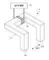
図1は、本発明の一実施形態に係る抵抗溶接方法が適用されたスポット溶接システム1の構成を示す図である。Hereinafter, embodiments of the present invention will be described with reference to the drawings.
FIG. 1 is a diagram showing a configuration of a
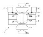
スポット溶接システム1は、剛性の異なる複数の板材、ここでは3枚の板材を重ね合わせて形成された溶接ワーク2を抵抗溶接するものである。
ここで、溶接ワーク2は、金属製の板材としての厚板21と、この厚板21と剛性および厚みが等しい金属製の厚板22と、厚板21、22よりも剛性が低く薄い金属製の板材としての薄板23と、を重ね合わせて形成されている。The
Here, the
スポット溶接システム1は、溶接ワーク2を抵抗溶接する抵抗溶接部3と、溶接ワーク2の内部に磁場を生じさせる磁場発生部4と、を備える。 The
抵抗溶接部3は、溶接ワーク2を挟んで配置された一対の溶接電極31、32と、これら溶接電極31、32を互いに接近、離隔させる駆動機構33と、溶接電極31、32に電流を供給する溶接電源34と、を備える。
具体的には、溶接電極31は、厚板21側に配置され、溶接電極32は、薄板23側に配置されている。The
Specifically, the
図2は、磁場発生部4の構成を示す図である。
磁場発生部4は、電磁石であり、馬蹄形の芯部41と、この芯部41に電線が巻かれて形成されたコイル42と、コイル42に接続された電磁石用電源43と、を備える。
芯部41の両端は、磁極411、412であり、溶接ワーク2の薄板23の表面上に溶接電極32を挟んで配置される。
なお、磁極411、412は、直接、薄板23に接触しておらず、溶接ワーク2の表面に対して絶縁されている。具体的には、磁極411、412と薄板23との間に絶縁材44が介装されている(図1参照)。なお、本実施形態では、絶縁材44を介装したが、これに限らず、磁極411、412を薄板23から離して配置してもよい。FIG. 2 is a diagram illustrating a configuration of the magnetic field generation unit 4.
The magnetic field generation unit 4 is an electromagnet, and includes a horseshoe-
Both ends of the
The
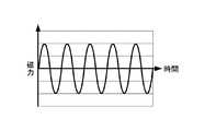
電磁石用電源43は、交流電源であり、交流を供給することにより、磁極411、412間に磁場を発生させる。この磁力の変化を示す波形は、図3に示すように、サインカーブであり、磁場の強さや向きが常に変化する。 The
以上のスポット溶接システム1の動作を説明する。
まず、図4に模式的に示すように、駆動機構33を駆動して、溶接電極31、32で溶接ワーク2を加圧して、この溶接ワーク2を挟持する。The operation of the above
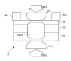
First, as schematically shown in FIG. 4, the
すると、厚板21、22は撓んで互いに反り返り、これら厚板21、22同士の接触面積は、A1となる。これに対し、薄板23は、厚板22に重ねて配置されているため、この厚板22になじんで変形する。その結果、薄板23と厚板22との接触面積は、厚板21、22同士の接触面積A1よりも大きいA2となり、薄板23と厚板22との接触抵抗は、厚板21、22同士の接触抵抗よりも小さくなる。 Then, the
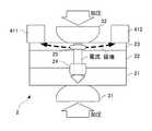
この状態で、図5に示すように、溶接電源34を駆動して、溶接電極31、32間に通電するとともに、電磁石用電源43を駆動して、磁極411、412間に磁場を生じさせる。すると、この磁場は、薄板23内部において、溶接電極31、32間に流れる電流の経路を横断することになる。 In this state, as shown in FIG. 5, the
すると、厚板21、22間の接触抵抗は、薄板23と厚板22との接触抵抗よりも大きいため、図6に示すように、主に厚板21、22間で発熱し、この厚板21、22間には、溶融部24が生じる。 Then, since the contact resistance between the
また、磁極411、412間に生じた磁場は、薄板23内部において、溶接電極31、32間の電流経路を横断するので、溶接電極31、32間を流れる電流には、磁場によりローレンツ力が作用する。よって、図7に模式的に示すように、薄板23内部では、電流の経路が乱れて、電子の移動距離が長くなるので、薄板23の内部抵抗が増大し、薄板23の内部には、発熱により溶融部25が生じる。 Further, since the magnetic field generated between the
その後、厚板21、22間に生じた溶融部24は、次第に成長し、図8に示すように、薄板23内部の溶融部25まで到達する。その結果、図9に示すように、溶融部24は、溶融部25と完全に一体化し、薄板23にも十分な溶け込みが得られる。 Thereafter, the melted
本実施形態によれば、以下のような効果がある。
(1)溶接電極31、32間に通電するとともに、これら溶接電極31、32間の電流経路を横断するように磁場を生じさせた。よって、溶接電極間に流れる電流には、磁場によりローレンツ力が作用し、電流の経路が乱れて、電子の移動距離が長くなる。その結果、溶接ワーク2の内部抵抗が増大し、溶接ワーク2の内部の発熱が促進されることとなる。よって、厚板22と薄板23との剛性が異なることにより接触面積が広くなっても、薄板23の内部抵抗を増大して薄板23内部の発熱を促進できるから、これらの板材21、22、23を確実に溶接できる。According to this embodiment, there are the following effects.
(1) While energizing between the
(2)磁場発生部4により、磁力をサインカーブに沿って変化させたので、磁場の強さや向きが常に変化し、ローレンツ力の作用する方向が常に変化するから、電子の移動経路を長くすることができ、内部抵抗を大きくして、薄板23内部での発熱量を増大できる。 (2) Since the magnetic force is changed along the sine curve by the magnetic field generator 4, the strength and direction of the magnetic field always change, and the direction in which the Lorentz force acts always changes, so the electron movement path is lengthened. The internal resistance can be increased, and the amount of heat generated in the
なお、本発明は前記実施形態に限定されるものではなく、本発明の目的を達成できる範囲での変形、改良等は本発明に含まれるものである。
例えば、上述の実施形態では、磁場における磁力の波形をサインカーブとしたが、これに限らず、矩形状としてもよい。It should be noted that the present invention is not limited to the above-described embodiment, and modifications, improvements, etc. within a scope that can achieve the object of the present invention are included in the present invention.
For example, in the above-described embodiment, the waveform of the magnetic force in the magnetic field is a sine curve, but the present invention is not limited to this and may be a rectangular shape.
また、本実施形態では、厚板21、22間に生じた溶融部24を成長させて、薄板23内部の溶融部25まで到達させたが、これに限らない。すなわち、溶接電源34および電磁石用電源43を調整することにより、厚板21、22間に生じた溶融部24だけではなく、薄板23内部の溶融部25も成長させて、これら溶融部24と溶融部25とを一体化させてもよい。 Further, in the present embodiment, the melted
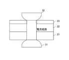
また、本実施形態では、3枚の板材21、22、23を重ね合わせて溶接ワーク2を形成したが、これに限らない。例えば、溶接ワークを2枚の板材で形成してもよい。具体的には、図10に示すように、溶接ワーク2Aを、厚板51と、この厚板51よりも剛性が低く薄い薄板52と、を重ね合わせて形成する。そして、この溶接ワーク2Aを溶接電極31、32で挟持し、溶接電極31、32間に通電するとともに、磁極411、412間に磁場を生じさせる。すると、厚板51と薄板52との間で発熱するとともに、薄板52の内部でも発熱し、薄板52の内部から厚板51に亘って溶融部26が発生する。 Moreover, in this embodiment, although the three board |
2 溶接ワーク
21、22 厚板(板材)
23 薄板(板材)
31、32 溶接電極(電極)
2 Welding
23 Thin plate (plate material)
31, 32 Welding electrode (electrode)
Claims (2)
Translated fromJapanese前記一対の電極間に通電中、当該一対の電極間の電流経路を横断するように磁場を生じさせることを特徴とする抵抗溶接方法。A resistance welding method for resistance welding the welded workpiece by energizing between the pair of electrodes in a state where a plurality of plate materials are overlapped to form a welded workpiece and the welded workpiece is sandwiched between the pair of electrodes,
A resistance welding method, wherein a magnetic field is generated so as to cross a current path between the pair of electrodes during energization between the pair of electrodes.
前記一対の電極間に通電中、前記磁場の強さおよび向きのうち少なくとも一方を変化させることを特徴とする抵抗溶接方法。
The resistance welding method according to claim 1,
A resistance welding method characterized by changing at least one of the strength and direction of the magnetic fieldduring energization between the pair of electrodes .
Priority Applications (1)
| Application Number | Priority Date | Filing Date | Title |
|---|---|---|---|
| JP2007091468AJP5128159B2 (en) | 2007-03-30 | 2007-03-30 | Resistance welding method |
Applications Claiming Priority (1)
| Application Number | Priority Date | Filing Date | Title |
|---|---|---|---|
| JP2007091468AJP5128159B2 (en) | 2007-03-30 | 2007-03-30 | Resistance welding method |
Publications (2)
| Publication Number | Publication Date |
|---|---|
| JP2008246538A JP2008246538A (en) | 2008-10-16 |
| JP5128159B2true JP5128159B2 (en) | 2013-01-23 |
Family
ID=39972106
Family Applications (1)
| Application Number | Title | Priority Date | Filing Date |
|---|---|---|---|
| JP2007091468AExpired - Fee RelatedJP5128159B2 (en) | 2007-03-30 | 2007-03-30 | Resistance welding method |
Country Status (1)
| Country | Link |
|---|---|
| JP (1) | JP5128159B2 (en) |
Cited By (1)
| Publication number | Priority date | Publication date | Assignee | Title |
|---|---|---|---|---|
| WO2024056980A1 (en)* | 2022-09-16 | 2024-03-21 | Gaming Engineering | Spot welding method |
Families Citing this family (12)
| Publication number | Priority date | Publication date | Assignee | Title |
|---|---|---|---|---|
| JP5427074B2 (en) | 2009-03-31 | 2014-02-26 | 本田技研工業株式会社 | Resistance welding method and apparatus |
| JP5411792B2 (en)* | 2009-06-05 | 2014-02-12 | 本田技研工業株式会社 | Resistance welding method and apparatus |
| JP2011194453A (en)* | 2010-03-23 | 2011-10-06 | Honda Motor Co Ltd | Seam welding method and device therefor |
| JP5554197B2 (en)* | 2010-09-29 | 2014-07-23 | 本田技研工業株式会社 | Spot welding method and apparatus |
| CN104302434B (en) | 2012-05-18 | 2017-05-17 | 本田技研工业株式会社 | Spot welding device and spot welding method |
| JP2014028392A (en) | 2012-06-29 | 2014-02-13 | Kobe Steel Ltd | Spot welding method |
| KR101406547B1 (en) | 2012-08-22 | 2014-06-11 | 주식회사 포스코 | Welding apparatus and welding electrode |
| CN103028829B (en)* | 2012-12-14 | 2015-09-09 | 浙江天齐电气有限公司 | The quick accurate welding system of distributing box |
| DE102013014701A1 (en)* | 2013-09-05 | 2015-03-05 | GM Global Technology Operations LLC (n. d. Ges. d. Staates Delaware) | Welding assembly for welding a connection portion and method for welding the connection portion to the welding assembly |
| CN116786961A (en)* | 2022-03-18 | 2023-09-22 | 新盛力科技股份有限公司 | How to weld the battery conductive frame to the battery core |
| EP4578585A1 (en) | 2022-09-29 | 2025-07-02 | JFE Steel Corporation | Resistance spot welding method and welded joint manufacturing method |
| CN119870670B (en)* | 2025-03-12 | 2025-09-05 | 广州弘一信息科技有限公司 | Resistance directional welding device based on electromagnetic principle |
- 2007
- 2007-03-30JPJP2007091468Apatent/JP5128159B2/ennot_activeExpired - Fee Related
Cited By (2)
| Publication number | Priority date | Publication date | Assignee | Title |
|---|---|---|---|---|
| WO2024056980A1 (en)* | 2022-09-16 | 2024-03-21 | Gaming Engineering | Spot welding method |
| FR3139742A1 (en)* | 2022-09-16 | 2024-03-22 | Gaming Engineering | Spot welding process |
Also Published As
| Publication number | Publication date |
|---|---|
| JP2008246538A (en) | 2008-10-16 |
Similar Documents
| Publication | Publication Date | Title |
|---|---|---|
| JP5128159B2 (en) | Resistance welding method | |
| JP3530322B2 (en) | Upward / vertical welding method | |
| JP5369150B2 (en) | Spot welding equipment | |
| JP2011125928A (en) | Laser welding method for steel sheet | |
| JP2009081980A (en) | Rotating electric machine and its stator | |
| JP6112209B2 (en) | Resistance spot welding method and manufacturing method of welded structure | |
| JP5411764B2 (en) | One-side resistance spot welding method and one-side resistance spot welding apparatus | |
| JP2015136731A (en) | Welding equipment | |
| JP5803116B2 (en) | Indirect spot welding method | |
| JP2011050977A (en) | Indirect spot welding method | |
| JP2012187616A (en) | Resistance welding apparatus and resistance welding method | |
| JP4753411B2 (en) | Energization control method for spot resistance welding | |
| JP5892390B2 (en) | Stud welding method and resistance welding machine | |
| JP5814906B2 (en) | Resistance welding method and resistance welding apparatus | |
| JP5930839B2 (en) | Resistance welding apparatus and resistance welding method | |
| JP2016059937A (en) | Spot welding equipment | |
| JP2014034059A (en) | Electromagnetic welding method for colliding metallic jets, and magnetic flux generating coil | |
| JP2907317B2 (en) | Laser welding method for railway vehicle structures | |
| JP7255119B2 (en) | Indirect spot welding device and welding method | |
| JP2012152821A (en) | Tabular one-turn coil for electromagnetic welding | |
| JP2012135775A (en) | Spot welding apparatus | |
| JP2013022623A (en) | Spot welding equipment and spot welding method | |
| WO2015037432A1 (en) | Resistance spot welding method and welded structure | |
| JP6049512B2 (en) | Spot welding method and spot welding apparatus | |
| JP7117814B2 (en) | Ground electrode for indirect spot welding |
Legal Events
| Date | Code | Title | Description |
|---|---|---|---|
| A621 | Written request for application examination | Free format text:JAPANESE INTERMEDIATE CODE: A621 Effective date:20091126 | |
| A131 | Notification of reasons for refusal | Free format text:JAPANESE INTERMEDIATE CODE: A131 Effective date:20120306 | |
| A521 | Request for written amendment filed | Free format text:JAPANESE INTERMEDIATE CODE: A523 Effective date:20120426 | |
| TRDD | Decision of grant or rejection written | ||
| A01 | Written decision to grant a patent or to grant a registration (utility model) | Free format text:JAPANESE INTERMEDIATE CODE: A01 Effective date:20121030 | |
| A01 | Written decision to grant a patent or to grant a registration (utility model) | Free format text:JAPANESE INTERMEDIATE CODE: A01 | |
| A61 | First payment of annual fees (during grant procedure) | Free format text:JAPANESE INTERMEDIATE CODE: A61 Effective date:20121031 | |
| R150 | Certificate of patent or registration of utility model | Free format text:JAPANESE INTERMEDIATE CODE: R150 Ref document number:5128159 Country of ref document:JP Free format text:JAPANESE INTERMEDIATE CODE: R150 | |
| FPAY | Renewal fee payment (event date is renewal date of database) | Free format text:PAYMENT UNTIL: 20151109 Year of fee payment:3 | |
| R250 | Receipt of annual fees | Free format text:JAPANESE INTERMEDIATE CODE: R250 | |
| LAPS | Cancellation because of no payment of annual fees |