JP5126741B2 - Field emission electron source - Google Patents
Field emission electron sourceDownload PDFInfo
- Publication number
- JP5126741B2 JP5126741B2JP2007335190AJP2007335190AJP5126741B2JP 5126741 B2JP5126741 B2JP 5126741B2JP 2007335190 AJP2007335190 AJP 2007335190AJP 2007335190 AJP2007335190 AJP 2007335190AJP 5126741 B2JP5126741 B2JP 5126741B2
- Authority
- JP
- Japan
- Prior art keywords
- electron source
- field emission
- cold cathode
- emission electron
- current
- Prior art date
- Legal status (The legal status is an assumption and is not a legal conclusion. Google has not performed a legal analysis and makes no representation as to the accuracy of the status listed.)
- Expired - Fee Related
Links
Images


Classifications
- H—ELECTRICITY
- H01—ELECTRIC ELEMENTS
- H01J—ELECTRIC DISCHARGE TUBES OR DISCHARGE LAMPS
- H01J1/00—Details of electrodes, of magnetic control means, of screens, or of the mounting or spacing thereof, common to two or more basic types of discharge tubes or lamps
- H01J1/02—Main electrodes
- H01J1/30—Cold cathodes, e.g. field-emissive cathode
- H01J1/304—Field-emissive cathodes
- H—ELECTRICITY
- H01—ELECTRIC ELEMENTS
- H01J—ELECTRIC DISCHARGE TUBES OR DISCHARGE LAMPS
- H01J9/00—Apparatus or processes specially adapted for the manufacture, installation, removal, maintenance of electric discharge tubes, discharge lamps, or parts thereof; Recovery of material from discharge tubes or lamps
- H01J9/02—Manufacture of electrodes or electrode systems
- H01J9/022—Manufacture of electrodes or electrode systems of cold cathodes
- H01J9/025—Manufacture of electrodes or electrode systems of cold cathodes of field emission cathodes
- H—ELECTRICITY
- H01—ELECTRIC ELEMENTS
- H01J—ELECTRIC DISCHARGE TUBES OR DISCHARGE LAMPS
- H01J2201/00—Electrodes common to discharge tubes
- H01J2201/30—Cold cathodes
- H01J2201/304—Field emission cathodes
- H01J2201/30446—Field emission cathodes characterised by the emitter material
Landscapes
- Engineering & Computer Science (AREA)
- Manufacturing & Machinery (AREA)
- Cold Cathode And The Manufacture (AREA)
Description
Translated fromJapanese本発明は、電界が印加されることにより電子を放出する電界放射型電子源に関するものである。 The present invention relates to a field emission electron source that emits electrons when an electric field is applied.
従来、透過電子顕微鏡、電子線描画装置、X線回折装置等に用いられ、電界が印加されることにより電子を放出する電界放射型電子源が知られている。前記電界放射型電子源の冷陰極から放出される電子の電流(放出電流)Jは、電界の強さをF、仕事関数をφ、定数をA、Bとしたときに、次式(1)で表される。 2. Description of the Related Art Conventionally, a field emission electron source that is used in a transmission electron microscope, an electron beam drawing apparatus, an X-ray diffraction apparatus, and the like and emits electrons when an electric field is applied is known. The current (emission current) J of electrons emitted from the cold cathode of the field emission electron source is expressed by the following equation (1), where F is the strength of the electric field, φ is the work function, and A and B are constants. It is represented by
J=A(F2/φ)exp[−Bφ3/2/F] ……(1)
前記式(1)によれば、仕事関数φを低くすることにより大きな放出電流Jを得ることができることが明らかである。J = A (F2 / φ) exp [−Bφ3/2 / F] (1)
According to the formula (1), it is clear that a large emission current J can be obtained by lowering the work function φ.
ところで、前記電界放射型電子源としては、タングステンからなる冷陰極に金属薄膜を被覆してなるものが知られている(例えば特許文献1参照)。前記電界放射型電子源は、タングステン単結晶(310)面の側面に純金薄膜と純アルミニウム薄膜とを被覆し、該(310)面の尖端にタングステン・金・アルミニウム三元合金薄膜とを被覆することにより、仕事関数φがタングステン(φ=5.5eV)よりも低くなり大きな放出電流Jを得ることができるとされている。 By the way, as the field emission type electron source, one obtained by coating a cold cathode made of tungsten with a metal thin film is known (for example, see Patent Document 1). In the field emission electron source, the side surface of the tungsten single crystal (310) is coated with a pure gold thin film and a pure aluminum thin film, and the tip of the (310) surface is coated with a tungsten / gold / aluminum ternary alloy thin film. Thus, the work function φ is lower than that of tungsten (φ = 5.5 eV), and a large emission current J can be obtained.
さらに大きな放出電流Jを得るには、前記冷陰極に、仕事関数φがタングステンより低い物質、例えば酸化バリウム、カーボン等をコーティングすることが考えられる。前記酸化バリウムの仕事関数φは2.0eVであり、前記カーボンの仕事関数φは4.5eVである。 In order to obtain a larger emission current J, it is conceivable that the cold cathode is coated with a material having a work function φ lower than that of tungsten, such as barium oxide or carbon. The barium oxide has a work function φ of 2.0 eV, and the carbon has a work function φ of 4.5 eV.
前記カーボンの一種として、例えば、カーボンナノチューブを挙げることができる。しかしながら、前記カーボンナノチューブを前記冷陰極にコーティングしてなる電界放射型電子源は、該カーボンチューブが容易にガス吸着を行うため,真空動作下において,該カーボンチューブから脱ガスが多量にかつ永続的におこり,安定な電界放射動作をすることは困難であるという問題がある。 An example of the carbon is a carbon nanotube. However, the field emission electron source formed by coating the carbon nanotubes on the cold cathode easily adsorbs gas in the carbon tube, and therefore, the degassing from the carbon tube is large and permanent under vacuum operation. Therefore, there is a problem that it is difficult to perform a stable field emission operation.
また,前記酸化バリウム、カーボン等の薄膜をコーティングした電界放射型電子源は,界面部分が脆弱化するため,電界を掛けた際に低電界で界面部分から放電が生じるため,電界放射型電子源の破壊が容易に起ってしまう問題を生じる。 In addition, the field emission electron source coated with a thin film such as barium oxide or carbon causes the interface portion to become weak, so that when the electric field is applied, a discharge occurs from the interface portion with a low electric field. This causes a problem that the destruction of the battery occurs easily.
更に,金属冷陰極と前記酸化バリウム、カーボン等の薄膜界面との間には接触抵抗が生じるため,低電流で放出電流の飽和が起こり,大きな放出電流Jを得ることは困難になるという問題も有する。
本発明は、上記事情に鑑み、小さな印加電圧で大きな放出電流を得ることができる電界放射型電子源を提供することを目的とする。 In view of the above circumstances, an object of the present invention is to provide a field emission electron source capable of obtaining a large emission current with a small applied voltage.
かかる目的を達成するために、本発明は、電界が印加されることにより電子を放出する電界放射型電子源において、冷陰極の尖端に、芳香族化合物の個々の分子を直立するように蒸着してなることを特徴とする。In order to achieve such an object, the present invention provides a field emission electron source that emits electrons when an electric field is applied, and depositsindividual molecules ofan aromatic compoundupright on the tip of a cold cathode. It is characterized by.
本発明によれば、電界が印加されたときに、前記冷陰極の尖端に直立するように蒸着された前記芳香族化合物の個々の分子から大量の電子を放出することができ、結果として、印加電圧が小さいときでも大きな放出電流を得ることができる。According to the present invention, when an electric field is applied, a large amount of electrons can be emitted fromindividual molecules of the aromatic compound depositedso as to standupright at the tip of the cold cathode. Even when the voltage is small, a large emission current can be obtained.
ここで、前記芳香族化合物の分子は、共役不飽和環を構成する原子が隣接する他の原子とsp2結合することにより平板構造を形成していて、該平板構造の分子の両面にπ電子の非局在化によるπ電子雲を備えている。前記芳香族化合物は、典型的には、前記共役不飽和環を構成する原子として炭素のみを含むものであり、このような化合物として、例えばベンゼンを挙げることができる。また、前記芳香族化合物は、前記共役不飽和環を構成する原子として、炭素の他に、窒素、リン、硫黄、酸素を含むものであってもよく、このような化合物として、例えばフラバントロンを挙げることができる。また、前記芳香族化合物は、複数の共役不飽和環の縮合環であってもよく、このような化合物として、例えばコロネン、ペンタセンを挙げることができる。さらに、前記芳香族化合物は、金属と錯体を形成しているものであってもよく、このような化合物として、例えばフタロシアニン、トリ−8−ハイドロキノリンアルミニウムを挙げることができる。Here, the molecule of the aromatic compound has a plate structure formed by sp2 bonding with atoms adjacent to the atoms adjacent to the conjugated unsaturated ring, and π electrons are formed on both sides of the molecule of the plate structure. Π electron cloud due to delocalization of The aromatic compound typically contains only carbon as an atom constituting the conjugated unsaturated ring, and examples of such a compound include benzene. Further, the aromatic compound may contain nitrogen, phosphorus, sulfur and oxygen in addition to carbon as atoms constituting the conjugated unsaturated ring. Can be mentioned. The aromatic compound may be a condensed ring of a plurality of conjugated unsaturated rings, and examples of such a compound include coronene and pentacene. Furthermore, the aromatic compound may form a complex with a metal, and examples of such a compound include phthalocyanine and tri-8-hydroquinoline aluminum.
前記電界放射型電子源において、前記平板構造を有する個々の前記芳香族化合物の分子は、前記冷陰極の尖端に対して直立するように蒸着されると考えられる。この結果、電界が印加されたときに、前記平板構造の分子の先端に電界集中が発生し、該電界集中により前記π電子が引き抜かれ、大きな放出電流を得ることができると考えられる。 In the field emission electron source, it is considered that the molecules of the aromatic compound having the flat plate structure are deposited so as to stand upright with respect to the tip of the cold cathode. As a result, it is considered that when an electric field is applied, an electric field concentration is generated at the tip of the molecule having the flat plate structure, and the π electrons are extracted by the electric field concentration, so that a large emission current can be obtained.
また、本発明において、前記冷陰極は、例えば、タングステン、チタン、タンタル、六ホウ化ランタンからなる群から選択される1種の材料を用いることができる。 In the present invention, for the cold cathode, for example, one material selected from the group consisting of tungsten, titanium, tantalum, and lanthanum hexaboride can be used.
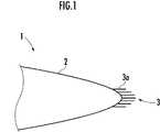
次に、添付の図面を参照しながら本発明の実施の形態についてさらに詳しく説明する。図1は本実施形態の電界放射型電子源を示す模式図であり、図2は本実施例の電界放射型電子源の放出電流を示すグラフであり、図3及び図4は本実施例の電界放射型電子源の放出電流の変動を示すグラフである。 Next, embodiments of the present invention will be described in more detail with reference to the accompanying drawings. FIG. 1 is a schematic diagram showing a field emission electron source of this embodiment, FIG. 2 is a graph showing the emission current of the field emission electron source of this example, and FIG. 3 and FIG. It is a graph which shows the fluctuation | variation of the emission current of a field emission type electron source.
図1に示す本実施形態の電界放射型電子源1は、タングステンからなる冷陰極2の尖端に、芳香族化合物の分子、例えばペンタセンの分子3aからなる蒸着膜3が形成されたものであり、図示しないチャンバ内に設けられている。 A field
電界放射型電子源1は、例えば次のようにして作成することができる。まず、(100)、(110)、(111)等の結晶面を有するタングステンからなる電極部材を用意し、該電極部材の表面を研磨することにより冷陰極2を形成する(例えば非特許文献1参照)。前記研磨は、例えば、電極部材を、水酸化アンモニウム溶液と水酸化カリウム溶液との混合溶液、又は水酸化カリウム溶液に浸漬した状態で、該電極部材を正電極として、該正電極に相対向する負電極との間に数VのAC電圧を印加することにより行うことができる。 The field
次に、冷陰極2を超高真空下でフラッシング処理することにより、冷陰極2の尖端に清浄表面を形成する。次に、冷陰極2の尖端に、ペンタセンの分子3aを蒸着することにより、蒸着膜3を形成する(例えば非特許文献2参照)。前記ペンタセンの分子3aの蒸着は、例えば、ペンタセンを搭載した蒸着ボード、又はペンタセンが塗布されたヒータに、真空下で冷陰極2の尖端を近接させるか、或いは、真空下でペンタセンの蒸気に冷陰極2の尖端を曝露することにより行うことができる。 Next, a clean surface is formed at the tip of the
本実施形態の電界放射型電子源1によれば、冷陰極2と該冷陰極2から所定間隔を有して配置された図示しない陽極との間に電圧が印加されることにより、電界が印加されたときに、冷陰極2の尖端に蒸着された蒸着膜3から大量の電子を放出することができ、結果として、印加電圧が小さいときでも大きな放出電流を得ることができる。 According to the field
蒸着膜3を構成するペンタセンは、芳香族化合物の一種である。前記芳香族化合物の分子は、共役不飽和環を構成する原子が隣接する他の原子とsp2結合することにより平板構造を形成していて、該平板構造の分子の両面にπ電子の非局在化によるπ電子雲を備えている。このため、電界放射型電子源1において、前記平板構造を有するペンタセンの分子3aは、冷陰極2の尖端に対して直立するように蒸着されると考えられる。この結果、電界が印加されたときに、前記平板構造のペンタセンの分子3aの先端に電界集中が発生し、該電界集中により前記π電子が引き抜かれ、大きな放出電流を得ることができると考えられる。Pentacene constituting the vapor deposition film 3 is a kind of aromatic compound. The molecule of the aromatic compound forms a plate structure by sp2 bonding with atoms adjacent to the atoms adjacent to the conjugated unsaturated ring, and π-electron non-localization is formed on both sides of the molecule of the plate structure. It has a π electron cloud by localization. For this reason, in the field
次に、本発明の実施例と比較例とを示す。 Next, examples of the present invention and comparative examples will be described.
まず、(011)の結晶面を有するタングステンからなり、長さが5mm、直径が0.1mmである電極部材を用意した。次に、濃度25wt%の水酸化アンモニウム溶液に前記電極部材を浸漬し、この状態で、該電極部材を正電極として、該正電極に相対向する円形の負電極との間に2〜3VのDC電圧を印加することにより、該電極部材の表面を電解研磨し、冷陰極2を形成した。 First, an electrode member made of tungsten having a crystal plane of (011) and having a length of 5 mm and a diameter of 0.1 mm was prepared. Next, the electrode member is immersed in an ammonium hydroxide solution having a concentration of 25 wt%, and in this state, the electrode member is used as a positive electrode, and a voltage of 2 to 3 V is provided between the positive electrode and a circular negative electrode facing the positive electrode. By applying a DC voltage, the surface of the electrode member was electropolished to form the
次に、冷陰極2を、10−8Paの超高真空下で通電加熱を用いてフラッシング処理することにより、冷陰極2に清浄表面を形成した。次に、10−8Paの真空下に10−6Paのペンタセンの蒸気を供給し、該ペンタセンの蒸気に冷陰極2の尖端を数秒曝露することにより、冷陰極2の尖端にペンタセンの分子3aからなる蒸着膜3を形成し、本実施例の電界放射型電子源1を完成させた。Next, a clean surface was formed on the
次に、本実施例の電界放射型電子源1に対して、300Kの温度で10−6Paの真空下において、冷陰極2と該冷陰極2から4mmの間隔を有して配置された図示しない陽極との間に電圧を印加することにより電界を発生させた。このとき、本実施例の電界放射型電子源1の放出電流を測定した。結果を図2に示す。Next, with respect to the field emission
さらに、冷陰極2と図示しない前記陽極との間に10kVの電圧を印加した状態で保持し、本実施例の電界放射型電子源1の放出電流の変動を測定した。結果を図3に示す。 Furthermore, the voltage of 10 kV was applied between the
次に、本実施例の電界放射型電子源1に対して、500Kの温度で10−6Paの真空下において、冷陰極2と図示しない前記陽極との間に10kVの電圧を印加した状態で保持し、本実施例の電界放射型電子源1の放出電流の変動を測定した。結果を図4に示す。
〔比較例〕
まず、前記実施例と全く同一にして、タングステンからなる冷陰極を形成し、これを本比較例の電界放射型電子源とした。本比較例の電界放射型電子源の冷陰極の尖端には、前記芳香族化合物の分子は蒸着されていない。Next, a voltage of 10 kV was applied between the
[Comparative Example]
First, a cold cathode made of tungsten was formed in exactly the same manner as in the previous example, and this was used as the field emission electron source of this comparative example. No molecule of the aromatic compound is deposited on the tip of the cold cathode of the field emission electron source of this comparative example.
次に、300Kの温度で10−6Paの真空下において、前記冷陰極と該冷陰極から4mmの間隔を有して配置された図示しない陽極との間に電圧を印加することにより電界を発生させた。このとき、本比較例の電界放射型電子源の放出電流を測定した。結果を図2に示す。Next, an electric field is generated by applying a voltage between the cold cathode and an anode (not shown) arranged at a distance of 4 mm from the cold cathode under a vacuum of 10−6 Pa at a temperature of 300 K. I let you. At this time, the emission current of the field emission electron source of this comparative example was measured. The results are shown in FIG.
図2から、印加電圧が約2000eVであるときには、比較例の電界放射型電子源によれば約7×10⁻¹⁰Aの放出電流を得ることができ、実施例の電界放射型電子源1によれば比較例に対して約104倍である約1×10⁻⁶Aの放出電流を得ることができることが明らかである。また、1×10⁻⁷Aの放出電流を得るためには、比較例の電界放射型電子源によれば約8000eVの印加電圧を必要とするが、実施例の電界放射型電子源1によれば比較例に対して約1/4である約2000eVの印加電圧でよく、小さな印加電圧で大きな放出電流を得ることができることが明らかである。From FIG. 2, when the applied voltage is about 2000 eV, according to the field emission electron source of the comparative example, an emission current of about 7 × 10⁻¹⁰ A can be obtained. Therefore, it is apparent that an emission current of about 1 × 10⁻⁶ A, which is about 104 times that of the comparative example, can be obtained. Further, in order to obtain an emission current of 1 × 10⁻⁷ A, an applied voltage of about 8000 eV is required according to the field emission electron source of the comparative example, but according to the field
また、図3から、実施例の電界放射型電子源1によれば、温度が300Kであるときには、放出電流が0.4〜0.98mAの範囲であって変動が大きいことが明らかである。また、電流値が突然上昇するスパイク状ノイズと、電流値が所定時間安定的に増加して一定値を示すステップ状ノイズとが発生していることが明らかである。一方、実施例の電界放射型電子源1によれば、温度が500Kであるときには、放出電流が0.5〜0.6mAの範囲であって変動が小さいことが明らかである。また、スパイク状ノイズとステップ状ノイズとがほとんど発生していないことが明らかである。 From FIG. 3, it is clear that according to the field
前記スパイク状ノイズ及び前記ステップ状ノイズは、ステップ・スパイク状ノイズと呼ばれ、冷陰極の尖端に炭素系の物質が蒸着された電界放射型電子源に特徴的な電流変動現象である。温度が300Kのときに発生した前記電流変動現象(図3)の原因は、前記チャンバ内の残留ガスの分子3aが電界放射型電子源1に吸着することにより、該電界放射型電子源1の仕事関数φが低下するためであると考えられる。そこで、前記残留ガスの分子3aの電界放射型電子源1への吸着頻度を減らすために、蒸着膜3のペンタセン分子3aが蒸発しない程度の温度である500Kに上昇させると、図4に示すように前記電流変動現象の発生を抑制することができる。 The spike noise and the step noise are referred to as step spike noise, which is a current fluctuation phenomenon characteristic of a field emission electron source in which a carbon-based material is deposited on the tip of a cold cathode. The cause of the current fluctuation phenomenon (FIG. 3) that occurs when the temperature is 300K is that the residual gas molecules 3a in the chamber are adsorbed to the field
以上から、本実施例の電界放射型電子源1においては、蒸着膜3のペンタセン分子3aが蒸発しない程度の温度に加熱することにより、長時間に亘って安定した放出電流を得ることができることが明らかである。 From the above, in the field
本実施形態では、冷陰極2としてタングステンを用いているが、チタン、タンタル、六ホウ化ランタン等を用いてもよい。また、蒸着膜3を構成する芳香族化合物としては、ペンタセンに代えて、例えば、ベンゼン、フタロシアニン、フラバントロン、トリ−8−ハイドロキノリンアルミニウム、コロネン、オリゴチオフェン、アントラセン、ペリレン、AlQ3、エチレン、アセチレン、ポリアセチレン、ビレン、ベンゾキノン、アントラキノン、アミノピロリジン、ハロビリジン、ビラジン、インドール、キノリン、スチルベン、テトラフェニルナフタセン、ジフェニルアントラセン、テトラフェニルベンジン、からなる群から選択される1種の化合物を用いてもよい。 In the present embodiment, tungsten is used as the
1…電界放射型電子源、 2…冷陰極、 3a…芳香族化合物の分子。 DESCRIPTION OF
Claims (3)
Translated fromJapanese冷陰極の尖端に、芳香族化合物の個々の分子を直立するように蒸着してなることを特徴とする電界放射型電子源。In a field emission electron source that emits electrons when an electric field is applied,
A field emission type electron source characterized in thatindividual molecules ofan aromatic compound are vapor-deposited on the tip ofa cold cathode so as to standupright .
Priority Applications (2)
| Application Number | Priority Date | Filing Date | Title |
|---|---|---|---|
| JP2007335190AJP5126741B2 (en) | 2007-12-26 | 2007-12-26 | Field emission electron source |
| US12/343,396US8405294B2 (en) | 2007-12-26 | 2008-12-23 | Field emission electron source |
Applications Claiming Priority (1)
| Application Number | Priority Date | Filing Date | Title |
|---|---|---|---|
| JP2007335190AJP5126741B2 (en) | 2007-12-26 | 2007-12-26 | Field emission electron source |
Publications (2)
| Publication Number | Publication Date |
|---|---|
| JP2009158304A JP2009158304A (en) | 2009-07-16 |
| JP5126741B2true JP5126741B2 (en) | 2013-01-23 |
Family
ID=40962090
Family Applications (1)
| Application Number | Title | Priority Date | Filing Date |
|---|---|---|---|
| JP2007335190AExpired - Fee RelatedJP5126741B2 (en) | 2007-12-26 | 2007-12-26 | Field emission electron source |
Country Status (2)
| Country | Link |
|---|---|
| US (1) | US8405294B2 (en) |
| JP (1) | JP5126741B2 (en) |
Families Citing this family (3)
| Publication number | Priority date | Publication date | Assignee | Title |
|---|---|---|---|---|
| US8730823B2 (en) | 2011-06-24 | 2014-05-20 | Jasper Wireless, Inc. | Core services platform for wireless voice, data and messaging network services |
| JP6028277B2 (en)* | 2012-07-30 | 2016-11-16 | 国立研究開発法人物質・材料研究機構 | Metal boride field emitter fabrication method |
| JP6325904B2 (en)* | 2014-06-02 | 2018-05-16 | キヤノン株式会社 | Solid-state imaging device manufacturing method, solid-state imaging device, and camera |
Family Cites Families (17)
| Publication number | Priority date | Publication date | Assignee | Title |
|---|---|---|---|---|
| US5726524A (en)* | 1996-05-31 | 1998-03-10 | Minnesota Mining And Manufacturing Company | Field emission device having nanostructured emitters |
| DE69728410T2 (en)* | 1996-08-08 | 2005-05-04 | William Marsh Rice University, Houston | MACROSCOPICALLY MANIPULATED DEVICES MANUFACTURED FROM NANOROE ASSEMBLIES |
| JPH11297189A (en) | 1998-04-10 | 1999-10-29 | Jeol Ltd | Field emission cold cathode and method of manufacturing the same |
| JP3494583B2 (en) | 1999-01-13 | 2004-02-09 | 松下電器産業株式会社 | Method for manufacturing electron-emitting device |
| US6265722B1 (en)* | 1999-08-31 | 2001-07-24 | Micron Technology, Inc. | Organic field ionization source |
| US6521324B1 (en)* | 1999-11-30 | 2003-02-18 | 3M Innovative Properties Company | Thermal transfer of microstructured layers |
| JP2002179418A (en)* | 2000-12-13 | 2002-06-26 | Tohoku Techno Arch Co Ltd | How to make carbon nanotubes |
| CA2450778A1 (en)* | 2001-06-14 | 2003-10-16 | Hyperion Catalysis International, Inc. | Field emission devices using modified carbon nanotubes |
| KR20030060611A (en)* | 2002-01-10 | 2003-07-16 | 삼성전자주식회사 | Field emitter device comprising carbon nanotube with protective membrane |
| JP2005032500A (en)* | 2003-07-10 | 2005-02-03 | Hitachi High-Technologies Corp | Cold cathode, electron source and electron beam apparatus using the same |
| US20050067936A1 (en)* | 2003-09-25 | 2005-03-31 | Lee Ji Ung | Self-aligned gated carbon nanotube field emitter structures and associated methods of fabrication |
| US7312562B2 (en)* | 2004-02-04 | 2007-12-25 | Chevron U.S.A. Inc. | Heterodiamondoid-containing field emission devices |
| JP4658490B2 (en)* | 2004-02-26 | 2011-03-23 | 大研化学工業株式会社 | Electron source and manufacturing method thereof |
| JP2005276498A (en)* | 2004-03-23 | 2005-10-06 | Fuji Xerox Co Ltd | Electron beam generating device and its manufacturing method |
| JP2006331997A (en)* | 2005-05-30 | 2006-12-07 | Dialight Japan Co Ltd | Electron source and electron beam application device equipped with the same |
| TWI435358B (en)* | 2005-08-10 | 2014-04-21 | Pureron Japan Co Ltd | A carbon film having a shape suitable for the emission of electric field, a carbon film structure, and an electron emitter |
| KR20070106231A (en)* | 2006-04-28 | 2007-11-01 | 삼성에스디아이 주식회사 | A composition for forming an electron emission source, a method for producing an electron emission source using the same, an electron emission source and an electron emission device manufactured by the method |
- 2007
- 2007-12-26JPJP2007335190Apatent/JP5126741B2/ennot_activeExpired - Fee Related
- 2008
- 2008-12-23USUS12/343,396patent/US8405294B2/ennot_activeExpired - Fee Related
Also Published As
| Publication number | Publication date |
|---|---|
| JP2009158304A (en) | 2009-07-16 |
| US8405294B2 (en) | 2013-03-26 |
| US20100033072A1 (en) | 2010-02-11 |
Similar Documents
| Publication | Publication Date | Title |
|---|---|---|
| US7997950B2 (en) | Field emission electron source having carbon nanotubes and method for manufacturing the same | |
| US7129513B2 (en) | Field emission ion source based on nanostructure-containing material | |
| JP3832402B2 (en) | Electron source having carbon nanotubes, electron microscope and electron beam drawing apparatus using the same | |
| US7988515B2 (en) | Method for manufacturing field emission electron source having carbon nanotubes | |
| JP3933035B2 (en) | Carbon nanotube manufacturing apparatus and manufacturing method | |
| US8029328B2 (en) | Method for manufacturing field emission electron source having carbon nanotubes | |
| JP2003217516A (en) | Field emission device provided with carbon nanotube having protective film | |
| Yeong et al. | Field-emission properties of ultrathin 5nm tungsten nanowire | |
| Dorozhkin et al. | Field emission from individual B–C–N nanotube rope | |
| JP5126741B2 (en) | Field emission electron source | |
| US6441550B1 (en) | Carbon-based field emission electron device for high current density applications | |
| US7932477B2 (en) | Electron beam heating system having carbon nanotubes | |
| JP2003095625A (en) | Method for making carbon nanotube, carbon nanotube and electron emitting source | |
| JP2001048509A (en) | CNT, CNT aggregate, field emission type cold cathode electron emitting device, method of manufacturing the same, and display device using the electron emitting device | |
| Kato et al. | Stable and high current density electron emission using coniferous carbon nano-structured emitter | |
| Yeong et al. | Life cycle of a tungsten cold field emitter | |
| Takikawa et al. | Carbon nanotubes in cathodic vacuum arc discharge | |
| CN111048383B (en) | Electron Source and Electron Gun | |
| JP2010015966A (en) | Electron-emitting element, electron gun, electron microscope device using it, and electron beam lithogrphy device | |
| JP2002352694A (en) | Electrode, electron emission element and device using it | |
| JP2019071260A (en) | Electron source, electron beam irradiation apparatus, and manufacturing method of electron source | |
| WO2007000919A1 (en) | Diamond electron source with carbon termination structure and production method thereof | |
| Kim et al. | Developmoent of high-temperature endurable CNT emitter for a cold cathode X-ray tube | |
| Bellucci et al. | Emission characteristics of carbon nanotubes at large electrode distances | |
| Murata et al. | Improvement of Electron Emission Properties of Volcano-Structured Silicon Emitters by Titanium Nitride Coating |
Legal Events
| Date | Code | Title | Description |
|---|---|---|---|
| A621 | Written request for application examination | Free format text:JAPANESE INTERMEDIATE CODE: A621 Effective date:20101213 | |
| A977 | Report on retrieval | Free format text:JAPANESE INTERMEDIATE CODE: A971007 Effective date:20111214 | |
| A131 | Notification of reasons for refusal | Free format text:JAPANESE INTERMEDIATE CODE: A131 Effective date:20111220 | |
| A521 | Written amendment | Free format text:JAPANESE INTERMEDIATE CODE: A523 Effective date:20120217 | |
| TRDD | Decision of grant or rejection written | ||
| A01 | Written decision to grant a patent or to grant a registration (utility model) | Free format text:JAPANESE INTERMEDIATE CODE: A01 Effective date:20121002 | |
| A01 | Written decision to grant a patent or to grant a registration (utility model) | Free format text:JAPANESE INTERMEDIATE CODE: A01 | |
| A61 | First payment of annual fees (during grant procedure) | Free format text:JAPANESE INTERMEDIATE CODE: A61 Effective date:20121022 | |
| R150 | Certificate of patent or registration of utility model | Free format text:JAPANESE INTERMEDIATE CODE: R150 Ref document number:5126741 Country of ref document:JP Free format text:JAPANESE INTERMEDIATE CODE: R150 | |
| FPAY | Renewal fee payment (event date is renewal date of database) | Free format text:PAYMENT UNTIL: 20151109 Year of fee payment:3 | |
| R250 | Receipt of annual fees | Free format text:JAPANESE INTERMEDIATE CODE: R250 | |
| R250 | Receipt of annual fees | Free format text:JAPANESE INTERMEDIATE CODE: R250 | |
| R250 | Receipt of annual fees | Free format text:JAPANESE INTERMEDIATE CODE: R250 | |
| R250 | Receipt of annual fees | Free format text:JAPANESE INTERMEDIATE CODE: R250 | |
| R250 | Receipt of annual fees | Free format text:JAPANESE INTERMEDIATE CODE: R250 | |
| LAPS | Cancellation because of no payment of annual fees |