JP5121291B2 - Data transfer system - Google Patents
Data transfer systemDownload PDFInfo
- Publication number
- JP5121291B2 JP5121291B2JP2007112203AJP2007112203AJP5121291B2JP 5121291 B2JP5121291 B2JP 5121291B2JP 2007112203 AJP2007112203 AJP 2007112203AJP 2007112203 AJP2007112203 AJP 2007112203AJP 5121291 B2JP5121291 B2JP 5121291B2
- Authority
- JP
- Japan
- Prior art keywords
- data
- data transfer
- divided
- divided data
- memory
- Prior art date
- Legal status (The legal status is an assumption and is not a legal conclusion. Google has not performed a legal analysis and makes no representation as to the accuracy of the status listed.)
- Active
Links
Images


Classifications
- G—PHYSICS
- G06—COMPUTING OR CALCULATING; COUNTING
- G06F—ELECTRIC DIGITAL DATA PROCESSING
- G06F13/00—Interconnection of, or transfer of information or other signals between, memories, input/output devices or central processing units
- G06F13/14—Handling requests for interconnection or transfer
- G—PHYSICS
- G06—COMPUTING OR CALCULATING; COUNTING
- G06F—ELECTRIC DIGITAL DATA PROCESSING
- G06F13/00—Interconnection of, or transfer of information or other signals between, memories, input/output devices or central processing units
- G06F13/14—Handling requests for interconnection or transfer
- G06F13/20—Handling requests for interconnection or transfer for access to input/output bus
- G06F13/28—Handling requests for interconnection or transfer for access to input/output bus using burst mode transfer, e.g. direct memory access DMA, cycle steal
- G—PHYSICS
- G06—COMPUTING OR CALCULATING; COUNTING
- G06F—ELECTRIC DIGITAL DATA PROCESSING
- G06F13/00—Interconnection of, or transfer of information or other signals between, memories, input/output devices or central processing units
- G06F13/14—Handling requests for interconnection or transfer
- G06F13/36—Handling requests for interconnection or transfer for access to common bus or bus system
- G06F13/368—Handling requests for interconnection or transfer for access to common bus or bus system with decentralised access control
- G06F13/378—Handling requests for interconnection or transfer for access to common bus or bus system with decentralised access control using a parallel poll method
- G—PHYSICS
- G06—COMPUTING OR CALCULATING; COUNTING
- G06F—ELECTRIC DIGITAL DATA PROCESSING
- G06F3/00—Input arrangements for transferring data to be processed into a form capable of being handled by the computer; Output arrangements for transferring data from processing unit to output unit, e.g. interface arrangements
- G06F3/12—Digital output to print unit, e.g. line printer, chain printer
Landscapes
- Engineering & Computer Science (AREA)
- Theoretical Computer Science (AREA)
- Physics & Mathematics (AREA)
- General Engineering & Computer Science (AREA)
- General Physics & Mathematics (AREA)
- Human Computer Interaction (AREA)
- Electron Beam Exposure (AREA)
- Bus Control (AREA)
Description
Translated fromJapanese本発明は、データ転送装置を介して制御データを所定の装置に転送するデータ転送システムに関し、特に、大容量の制御データを高速に転送するデータ転送システムに関する。 The present invention relates to a data transfer system for transferring control data to a predetermined device via a data transfer device, and more particularly to a data transfer system for transferring a large amount of control data at high speed.
制御用ワークステーションで生成された大容量の制御データをデータ転送装置を介して被制御装置側に転送する場合、トータルスループットを向上させるために、高速データ転送が要求される。 When transferring a large amount of control data generated by the control workstation to the controlled device side via the data transfer device, high-speed data transfer is required to improve the total throughput.
この被制御装置として電子ビーム描画装置を例に説明すると、従来、制御用ワークステーションとデータ転送装置のインターフェースとのコネクション処理について、データ転送コマンド及び指定アドレスに書き込むデータをセットにしたサブコマンドと、サブコマンドの個数、語数、コントロールバイト、情報の転送時間等が含まれる複合コマンドヘッダを有する複合コマンドとを一つのフレームに作成し、このフレームを上記インターフェースに送信し、送信完了後に、インターフェース側から制御用ワークステーション側に応答コマンドを送信するデータ転送システム(データ転送方法、電子線装置)が提案されていた(例えば、特許文献1参照)。 The electron beam lithography apparatus will be described as an example of the controlled apparatus. Conventionally, with respect to the connection process between the control workstation and the interface of the data transfer apparatus, a data transfer command and a subcommand that sets data to be written to a specified address, A composite command having a composite command header including the number of subcommands, number of words, control byte, information transfer time, etc. is created in one frame, and this frame is transmitted to the above interface. A data transfer system (data transfer method, electron beam apparatus) that transmits a response command to the control workstation side has been proposed (for example, see Patent Document 1).
このシステムによれば、コマンドデータの転送の都度、コネクション処理をする必要がなくなり、実効的な転送速度を速くすることができる。 According to this system, it is not necessary to perform connection processing every time command data is transferred, and the effective transfer rate can be increased.
ところで、上記従来のデータ転送システム(図5参照)は、制御用ワークステーション4とデータ転送装置5との間のコネクション処理に関するものであるが、近年は、データ転送装置側でショット展開まで行うようになっているため、システム全体のスループットを向上させるためには、データ転送装置5と電子ビーム描画装置7との間のデータ転送速度も向上させる必要がある。 Incidentally, the conventional data transfer system (see FIG. 5) relates to the connection processing between the control workstation 4 and the
データ転送装置5と電子ビーム描画装置7との間のデータ転送は、大容量の制御データを転送する帯域を確保するために、この制御データを分割し、各分割データをデータ転送装置5に設けた複数のインターフェースから、各インターフェースに対応する複数の専用バスを介して、電子ビーム描画装置7のメモリ71に直接転送していた。例えば、1の専用バスにおけるデータ転送速度が200MB/sだとすると、制御データ全体で500MB/sを超える場合は、3つのインターフェース51a、51b及び51cと3つの専用バス6a、6b及び6cが必要になる。 In the data transfer between the
メモリ71は、3つのモジュール71a、71b及び71cに分割され、各々専用バス6a、6b及び6cに対応している。各モジュール71a、71b及び71cに格納された上記分割データに基づき、電子ビーム描画装置7を制御してフレームF1の矢印方向にステージを移動させてストライプの描画を行なう。1のストライプデータによる描画が終了すると、描画ステージが隣接するストライプ領域にステップ送りされ、新たなストライプ領域に割り当てられるストライプデータに基づき描画が行なわれる。以後、連続的に移動してこの描画動作を繰り返すことにより、所望のデバイスパターンをウェーハ上に描画する。
しかし、ストライプの描画方向のステージ移動速度は、ストライプ内で最も高いショット密度によって決まるため、上記従来の転送システムでは、一部の分割データの転送が遅れると、メモリの一部が開放されていても、分割データの処理の順番を維持するために同期をとる関係上、開放されたメモリを順次使用することができず、分割データの転送が停止し、全体の処理時間に無駄が生じるという不都合があった。 However, since the stage moving speed in the stripe drawing direction is determined by the highest shot density in the stripe, in the conventional transfer system, when the transfer of some divided data is delayed, a part of the memory is released. However, due to the synchronization in order to maintain the processing order of the divided data, the released memory cannot be used in sequence, and the transfer of the divided data is stopped, resulting in a waste of the entire processing time. was there.
たとえば、図5のフレームF2では、領域I及び領域IIIのショット密度に比べて、領域IIのショット密度が非常に高いため、フレームF2のステージ移動速度は、領域IIによって決定される。 For example, in the frame F2 in FIG. 5, the shot density in the region II is very high compared to the shot density in the region I and the region III, so the stage moving speed of the frame F2 is determined by the region II.
領域Iに対応する分割データはモジュール71aに、領域IIに対応する分割データはモジュール71bに、領域IIIに対応する分割データはモジュール71cに格納されている。 The divided data corresponding to the area I is stored in the
したがって、フレームF2では、領域I及び領域IIIの描画処理が終了しても、領域IIの描画処理が終了するまでは、モジュール71a及び71cに転送される次の分割データに基づいて描画処理を進めることができず、次のストライプ領域へのステップ送りを停止せざるをえなかった。 Therefore, in the frame F2, even if the drawing process for the area I and the area III is completed, the drawing process is advanced based on the next divided data transferred to the
また、電子ビーム描画装置のメモリが、モジュール単位に上記複数の専用バスと1対1で直結しているため、転送される分割データは、メモリ(モジュール)容量の制限を受けるという不都合もあった。仮に、上記メモリ容量を超えるデータが転送されると、電子ビーム描画装置の処理が停止してしまうという不具合もあった。 In addition, since the memory of the electron beam drawing apparatus is directly connected to the plurality of dedicated buses in a one-to-one manner in units of modules, there is a problem in that divided data to be transferred is limited by the memory (module) capacity. . If data exceeding the memory capacity is transferred, the processing of the electron beam drawing apparatus stops.
上記のような問題点は、電子ビーム描画装置に限らず、大容量の制御データを分割して、分割データの処理順番を制御する必要があるデータ転送システムに等しく生じる問題である。 The problems as described above are not limited to the electron beam drawing apparatus, and are problems that occur equally in a data transfer system that needs to divide a large amount of control data and control the processing order of the divided data.
そこで、本発明は以上のような従来技術の欠点に鑑み、大容量の制御データを分割し、データ転送装置と電子ビーム描画装置等の被制御装置との間で上記分割データの処理順番を制御して、メモリサイズに依存しない高速の転送処理を実現させるデータ転送システムを提供することを課題とする。 In view of the above-mentioned drawbacks of the prior art, the present invention divides a large amount of control data and controls the processing order of the divided data between the data transfer apparatus and the controlled apparatus such as an electron beam drawing apparatus. An object of the present invention is to provide a data transfer system that realizes high-speed transfer processing independent of the memory size.
本発明にかかるデータ転送システムは、装置制御データの分割データを生成する複数のデータ生成端末と、各データ生成端末と通信自在に接続され、各分割データの送信制御を行なうホスト端末と、上記の分割データをランダムに受信してメモリに格納し、汎用の高速データ転送バスに対応した拡張カードから上記の分割データを転送するデータ転送装置と、転送された分割データによって制御される電子ビーム描画装置とを備え、上記のデータ転送装置は、メモリに格納された分割データから、電子ビーム描画装置を制御するために、前記分割データを構成する情報のうち、転送する順番を特定する情報を読み出して、転送パラメータリストを生成するパラメータリスト生成手段と、拡張カードにこのパラメータリストを設定し、上記のメモリから高速データ転送バスを介してDMA転送された分割データを受信して、設定されたパラメータリストに記録された順番に従って分割データを電子ビーム描画装置側のメモリに転送する転送処理手段とを有していることを特徴とする。
A data transfer system according to the present invention includes a plurality of data generation terminals that generate divided data of device control data, a host terminal that is communicatively connected to each data generation terminal and performs transmission control of each divided data, A data transfer device that randomly receives divided data, stores it in a memory, and transfers the above-mentioned divided data from an expansion card compatible with a general-purpose high-speed data transfer bus, and anelectron beam drawing device controlled by the transferred divided data In order to control theelectron beam drawing apparatus , the above data transfer device reads out information specifying the transfer order from the information constituting the divided data from the divided data stored in the memory. The parameter list generating means for generating the transfer parameter list and the parameter list are set in the expansion card, and the above-mentioned menu is set. It receives divided data transferred by DMA over a high-speed data transfer bus from Li, organic and transferring unit that transfers the divided data to theelectron beam drawing apparatus memory in accordance with the order recorded in the set parameter list It is characterized by that.
上述のホスト端末、データ生成端末、データ転送装置は、いずれも汎用のパーソナルコンピュータを使用すればよく、データ転送装置の高速データ転送バスは、汎用のパーソナルコンピュータで採用されているバス規格、すなわち、PCI−XバスまたはPCIexpressであればよい。 The above-described host terminal, data generation terminal, and data transfer device may all use a general-purpose personal computer, and the high-speed data transfer bus of the data transfer device is a bus standard adopted by a general-purpose personal computer, that is, Any PCI-X bus or PCI express may be used.
この構成によれば、分割データを処理する順番を自動的に制御しつつ、高速転送することができる。 According to this configuration, high-speed transfer can be performed while automatically controlling the order of processing the divided data.
また、上述の分割データを転送する順番の情報は、たとえば、アドレス情報とデータサイズ情報とを各分割データから抽出すればよい。 Moreover, what is necessary is just to extract address information and data size information from each division data, for example as the information of the order of transferring the above-mentioned division data.
さらに、上述の大容量の制御データは、データ転送装置を複数使用することにより、さらに処理能力が向上するが、この場合、1のデータ転送装置で、転送先アドレスが連続していない複数の分割データを受信しても、上記パラメータリストを生成することができない。 Further, the processing capacity of the above-mentioned large-capacity control data can be further improved by using a plurality of data transfer devices. In this case, a single data transfer device can be divided into a plurality of divided transfer destination addresses. Even if data is received, the parameter list cannot be generated.
そこで、各データ転送装置の最大メモリサイズを超えない範囲で、連続するアドレス情報を有する複数の分割データをランダムにグループ化したブロックデータを形成し、このブロックデータ単位に各データ転送装置に送信する送信制御手段を上記ホスト端末が備えるようにすればよい。 Therefore, block data in which a plurality of divided data having continuous address information is randomly grouped within a range not exceeding the maximum memory size of each data transfer device is formed and transmitted to each data transfer device in units of this block data. The host terminal may be provided with transmission control means.
なお、ブロックデータ内の分割データは、転送時に、パラメータリストによって転送の順番が制御されるので、上記の通り、データ転送装置で受信するときには、ランダムにグループ化されていてよい。 In addition, since the order of transfer is controlled by the parameter list at the time of transfer, the divided data in the block data may be randomly grouped when received by the data transfer apparatus as described above.
また、上述の分割データの受信からパラメータリストの設定までの処理を実行している間は、データ転送装置は、被制御装置にデータを転送することができない。そこで、ブロックデータの転送とパラメータリストの生成及び設定とを異なるデータ転送装置で並行して処理し、順次連続して分割データが転送されるようにするために、ホスト端末の送信制御手段が、各データ生成端末から上記ブロックデータの送信のタイミングを制御すればよい。 In addition, the data transfer device cannot transfer data to the controlled device while executing the processing from the reception of the divided data to the setting of the parameter list. Therefore, in order to process block data transfer and parameter list generation and setting in parallel in different data transfer devices and sequentially transfer the divided data, the host terminal transmission control means, The transmission timing of the block data from each data generation terminal may be controlled.
さらに、上述のブロックデータが、被制御装置側のメモリサイズを超えていると、転送処理が停止する。そこで、被制御装置のメモリを一次元配列の複数のモジュールに分割して、各モジュールに多次元的にアドレスを付与するメモリバンクを形成し、ブロックデータが転送されると、ブロックデータを構成する各分割データを連続したアドレス空間に格納するために、アドレスを切換える切換手段を上記被制御装置に設ければよい。 Further, when the above block data exceeds the memory size on the controlled device side, the transfer process stops. Therefore, the memory of the controlled device is divided into a plurality of modules in a one-dimensional array to form a memory bank that gives addresses to each module in a multidimensional manner. When block data is transferred, block data is formed. In order to store each divided data in a continuous address space, switching means for switching addresses may be provided in the controlled device.
以上の説明から明らかなように、本発明にかかるデータ転送システムは、大容量の制御データを分割し、データ転送装置と電子ビーム描画装置等の被制御装置との間で分割データの処理順番を制御して、高速の転送処理の実現が可能になるという効果を奏する。 As is apparent from the above description, the data transfer system according to the present invention divides a large amount of control data, and sets the processing order of the divided data between the data transfer device and a controlled device such as an electron beam drawing device. It is possible to achieve high-speed transfer processing by controlling.
また、被制御装置側にメモリバンクを形成することにより、物理的なメモリサイズに制限されずに、複数のデータ転送装置から順次連続して分割データを転送することができるという効果を奏する。 Further, by forming the memory bank on the controlled device side, there is an effect that the divided data can be transferred sequentially from a plurality of data transfer devices without being limited by the physical memory size.
本実施の形態では、本発明にかかるデータ転送システムにつき、電子ビーム描画装置を制御するデータ転送システムによって説明するが、大容量の制御データを分割して、分割データの処理順番を制御するデータ転送システムであれば、電子ビーム描画装置以外のものでも適用可能である。 In this embodiment, the data transfer system according to the present invention will be described with reference to a data transfer system that controls an electron beam drawing apparatus. However, data transfer that divides a large amount of control data and controls the processing order of the divided data. Any system other than the electron beam drawing apparatus can be applied.
図1を参照して、1は、本発明にかかるデータ転送システムにおいて、制御データを分割した分割データの送信制御を行なうホスト端末である。この分割データは、ホスト端末1と通信自在にクラスター接続された複数データ生成端末1a、1b、1c…1nによって生成される。 Referring to FIG. 1, reference numeral 1 denotes a host terminal that performs transmission control of divided data obtained by dividing control data in the data transfer system according to the present invention. This divided data is generated by a plurality of
各データ生成端末1a、1b、1c…1nによって生成された分割データは、ホスト端末1の指令によってランダムにデータ転送装置2a、2b、2cに送信される。 The divided data generated by each of the
データ転送装置2b、2cは、2aと同じ構成であるため、以下、2aの構成について説明する。 Since the
21は、データ端末装置2aのメモリであり、ランダムに送信された上記複数の分割データがCPU24の命令により格納される場所である。
メモリ21に格納された分割データから、転送する順番の情報をパラメータリスト生成部22が読み出して、転送順番のメニューとなるパラメータリストを生成する。 From the divided data stored in the
パラメータリスト生成部22で生成されたパラメータリストは、転送処理部23に設定される。この転送処理部23は、たとえば、FPGA(Field Programmable Gate Array)プロセッサをベースにした拡張カード(汎用のパーソナルコンピュータに搭載可能なPCI−Xカード、PCIexpressカードなど)であればよい。この場合、転送処理部23の処理は、プログラムされたFPGAモジュールによって実行される。 The parameter list generated by the parameter
メモリ21に格納された各分割データは、CPU24の制御に基づき、チップセット25を介して転送処理部23に伝送される。チップセット25は、メモリ21とCPU24との間の制御を行なうメモリ制御部25aと、CPU24からメモリ21に格納されている分割データの読み込み要求に従って、バスマスタとしてCPU24に代わりDMA転送を制御するDMA制御部25bと、上述の拡張カードの接続制御を行なうバス制御部25cとを有する。 Each divided data stored in the
上述の分割データは、チップセット25と転送処理部23との間を高速データ転送バス26を介してDMA転送される。高速データ転送バス26は、上述の拡張カードに対応するPCI−XバスまたはPCIexpressバスであればよい。 The above-mentioned divided data is DMA-transferred between the
パラメータリストが設定された転送処理部23では、分割データを受信すると、パラメータリストに記録された順番に従って分割データを電子ビーム描画装置3に転送する。 In the
なお、ホスト端末1、データ生成端末1a、1b、1c…1n、データ転送装置2a、2b、2cは、いずれも汎用のパーソナルコンピュータを使用することができる。従って、図5で説明した制御用ワークステーション4とインターフェース51a、51b及び51cと専用バス6a、6b及び6cを備えたデータ転送装置5とから構成される従来のデータ転送システムに比べて、システム構築にかかるコストを抑えることができる。 The host terminal 1, the
電子ビーム描画装置3のメモリ31は、一次元配列の複数のモジュールに分割し、各モジュールに多次元的にアドレスが付与される複数のメモリバンク31a、31b、31c…31nが形成されている。 The
電子ビーム描画装置3に転送された各分割データは、アドレス情報に従って所定のメモリバンクにアクセスするために、切換部32によって上記所定のメモリバンクが割り当てられる。メモリ31に格納された分割データは、適宜電子ビーム描画装置本体33の描画動作を制御し、所望のパターンの描画を得ることができる。 Each divided data transferred to the electron
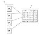
図2は、上記パラメータリストのイメージ図を示したものである。分割データは、転送順番に関係なく、メモリ21にランダムに格納される。図2では、メモリ21に分割データ2、分割データ1、分割データ3…分割データnという順番で格納されているが、電子ビーム描画装置3に転送するときには、分割データ1、分割データ2、分割データ3…分割データnに並び替える必要があるとする。 FIG. 2 shows an image diagram of the parameter list. The divided data is randomly stored in the
そこで、パラメータリスト生成手段22は、メモリ21に格納されている分割データ2、分割データ1、分割データ3…分割データnのアドレス情報及びサイズ情報を抽出し、転送する順番、すなわち、分割データ1、分割データ2、分割データ3…分割データnの順番に各分割データのアドレス情報及びサイズ情報を並び替えたパラメータリストを生成する。 Therefore, the parameter list generation means 22 extracts the address information and size information of the divided data 2, the divided data 1, the divided
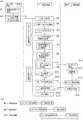
以下、図1、図2を参照しつつ、図3(a)を使用して、データ転送処理のフローを説明する。 The flow of data transfer processing will be described below with reference to FIGS. 1 and 2 and FIG. 3A.
データ生成端末1a、1b、1c…1nにより、複数の分割データが生成されると(S1)、ホスト端末1の送信制御に基づいてアドレスが連続した分割データをランダムにデータ転送装置2に送信する(S2)。 When a plurality of pieces of divided data are generated by the
データ転送装置2で分割データを受信して(S3)、メモリ21に格納する(S4)。ランダムに格納された分割データから、アドレス情報、サイズ情報を抽出してパラメータリストを生成する(S5)。生成されたパラメータリストは、転送処理部23に設定される(S6)。 The data transfer device 2 receives the divided data (S3) and stores it in the memory 21 (S4). A parameter list is generated by extracting address information and size information from the randomly stored divided data (S5). The generated parameter list is set in the transfer processing unit 23 (S6).
転送処理部23からメモリ21に分割データの転送要求信号を送信すると(S7)、メモリ21から転送処理部23に分割データがDMA転送される(S8)。 When a transfer request signal for divided data is transmitted from the
データ転送装置2は、パラメータリストの順番に従って分割データを電子ビーム描画装置3に転送する(S9)。 The data transfer apparatus 2 transfers the divided data to the electron
電子ビーム描画装置3では、この分割データを受信し(S11)、装置を制御して(S12)、所定のパターンが描画される。 The electron
このデータ転送処理の終了の有無を判断し(S10)、終了しない限り、S9とS10の処理を繰り返す。データ転送の終了が判断されると、終了フラグを立てて電子ビーム描画装置3に終了フラグ信号を送信する(S13)。 It is determined whether or not the data transfer process is finished (S10), and the processes of S9 and S10 are repeated unless the data transfer process is finished. When it is determined that the data transfer is completed, an end flag is set and an end flag signal is transmitted to the electron beam drawing apparatus 3 (S13).
電子ビーム描画装置3で、上記終了フラグ信号を受信すると(S14)、終了フラグの応答信号をデータ転送装置2に送信する(S15)。 When the electron
データ転送装置では、上記応答信号を受信すると(S16)、メモリ21を開放し(S17)、次の分割データを受信する準備ができる。 When the data transfer device receives the response signal (S16), it releases the memory 21 (S17) and is ready to receive the next divided data.
図3(b)は、複数のデータ転送装置を設けた場合のデータ転送のタイミングチャートを示した図である。 FIG. 3B is a diagram showing a timing chart of data transfer when a plurality of data transfer devices are provided.
図3(a)は、1台のデータ転送装置の転送処理フローを示したものであるが、S3〜S7の処理(以下「パラメータリスト設定処理」という)を実行している間は、CPUがこの処理に占有され、S8〜S17の処理(以下「データ転送処理」という)は実行できない。 FIG. 3A shows a transfer process flow of one data transfer apparatus. While the processes of S3 to S7 (hereinafter referred to as “parameter list setting process”) are being executed, the CPU Occupying this process, the processes of S8 to S17 (hereinafter referred to as “data transfer process”) cannot be executed.
そこで、複数のデータ転送装置を設けて、パラメータリスト設定処理とデータ転送処理とを異なるデータ転送処理装置で並行して処理し、順次連続して分割データが転送されるようにすればよい。 Therefore, a plurality of data transfer devices may be provided so that parameter list setting processing and data transfer processing are processed in parallel by different data transfer processing devices so that the divided data is sequentially transferred.
この連続した分割データ転送処理は、ホスト端末1(図1参照)の送信制御手段(図示せず)により、分割データの送信のタイミングを各データ転送装置に対してずらして行なえばよい。すなわち、上記送信制御手段は、第1データ転送装置1に分割データを送信した後、所定のタイミングで第2データ転送装置に別の分割データを送信する。 This continuous divided data transfer process may be performed by shifting the transmission timing of the divided data with respect to each data transfer device by the transmission control means (not shown) of the host terminal 1 (see FIG. 1). That is, the transmission control means transmits the divided data to the first data transfer apparatus 1 and then transmits another divided data to the second data transfer apparatus at a predetermined timing.
上述の所定のタイミングは、第1データ転送装置でパラメータリスト設定処理1が実行され、データ転送処理1の終了後、略連続して第2データ転送装置によるデータ転送処理2を開始することができるようなタイミングである。 At the above-mentioned predetermined timing, the parameter list setting process 1 is executed by the first data transfer apparatus, and after the data transfer process 1 is completed, the data transfer process 2 by the second data transfer apparatus can be started almost continuously. It is such a timing.
第3データ転送装置でも、第2転送装置によるデータ転送処理2の終了後、略連続して第3データ転送装置によるデータ転送処理3を開始できるようなタイミングで、分割データを第3データ転送装置に送信すればよい。 Even in the third data transfer device, the divided data is transferred to the third data transfer device at a timing at which the
上述した3つのデータ転送装置の動作周期を所定のタイミングでずらすことにより、データ転送処理1からデータ転送処理3までの連続したt時間でデータ転送を実行することができるため、従来のように間欠的にデータ転送処理する場合に比べて、高速のデータ転送を実現することができる。 By shifting the operation cycle of the three data transfer devices described above at a predetermined timing, data transfer can be executed in continuous t time from the data transfer processing 1 to the
図4は、分割データの転送動作を示したものである。本実施の形態では、分割データ1から分割データ5を複数のデータ転送装置で転送する形態を例として示した。なお、いずれの分割データも重複して記載されているが、2点鎖線で囲まれたものは動作履歴を示すものであり、実際に存在する場所には、実線で囲まれたもので示している。 FIG. 4 shows the divided data transfer operation. In the present embodiment, an example in which divided data 1 to divided
分割データ1はデータ生成端末1a、分割データ2はデータ生成端末1b、分割データ3はデータ生成端末1c、分割データ4はデータ生成端末1d、分割データ5はデータ生成端末1eによってそれぞれ生成され、ホスト端末1によってデータ転送装置2a及び2bに送信される。 The divided data 1 is generated by the data generating terminal 1a, the divided data 2 is generated by the data generating terminal 1b, the divided
なお、分割データを電子ビーム描画装置3に転送する順番は、分割データ1→分割データ2→分割データ3→分割データ4→分割データ5の順番とする。 The order in which the divided data is transferred to the electron
この場合、データ転送装置2aまたは2bで、アドレスが連続していない複数の分割データを受信しても、パラメータリストを生成することができない。 In this case, the parameter list cannot be generated even if the
そこで、データ転送装置2aまたは2bの最大メモリサイズを超えない範囲で、アドレスが連続した複数の分割データをランダムにグループ化してブロックデータを形成し、このブロックデータ単位に各データ転送装置に送信すればよい。 Therefore, block data is formed by randomly grouping a plurality of divided data having consecutive addresses within a range not exceeding the maximum memory size of the
データ転送装置2aの最大メモリサイズが、分割データ1から分割データ3までを格納することが可能な場合、分割データ1から分割データ3をブロックデータB1として格納する。同様に、データ転送装置2bでは、分割データ4、5をブロックデータB2として格納する。 When the maximum memory size of the
上記ブロックデータ内の分割データは、転送時にパラメータリストによって順番が制御されるので、データ転送装置2a及び2bに格納するときは、ランダムになっていてもよい。本実施の形態では、データ転送装置2aの格納時には、分割データ1、分割データ3、分割データ2の順番で格納され、データ転送装置2bの格納時には、分割データ5、分割データ4の順番で格納されている。
Since the order of the divided data in the block data is controlled by the parameter list at the time of transfer, it may be random when stored in the
ブロックデータB1及びブロックデータB2は、データ転送装置2aまたはデータ転送装置2bから電子ビーム描画装置3に転送されるときには、分割データの順番が制御されている。 When the block data B1 and the block data B2 are transferred from the
電子ビーム描画装置3のメモリ31は、複数のメモリバンク31a、…31nが形成され、各分割データは、転送される順番に従って切換部32の切換処理により、連続するアドレス空間として割り当てられる各メモリバンクに順次格納される。すなわち、メモリバンク31aに分割データ1が収納され、次いでメモリバンク31bに分割データ2が収納される。 The
図4では、分割データ1、分割データ2は、既に電子ビーム描画装置3を制御するためにメモリ31から読み出され、分割データ1が格納されていたメモリバンク31aに分割データ3の一部が格納され、分割データ2が格納されていたメモリバンク31bに分割データ3の残部がこれから格納される状態を示している。このように、開放されたメモリバンクに順次分割データを格納するため、メモリサイズに依存することなく、膨大な制御データでも対応可能になる。 In FIG. 4, the divided data 1 and the divided data 2 are already read from the
分割データ3は、本来、メモリバンク31cに格納されるべきであるが、メモリバンク31cが故障等により不具合がある場合は、切換部32は、メモリバンク31cを排除してアドレスを割り当てることができる。このように、故障等により、特定のメモリバンクをスキップしても、十分に機能させるようにするために、さらには、電子ビーム描画装置3内部の収納スペースやコストを考慮すると、少なくとも、メモリバンクは4つ以上備えるものが好ましい。 The divided
なお、各メモリバンクに格納する分割データのデータ量は、描画速度によって可変である。 Note that the data amount of the divided data stored in each memory bank is variable depending on the drawing speed.
1 ホスト端末
1a〜1n データ生成端末
2a〜2c データ転送装置
3 電子ビーム描画装置DESCRIPTION OF SYMBOLS 1
Claims (5)
Translated fromJapanesePriority Applications (3)
| Application Number | Priority Date | Filing Date | Title |
|---|---|---|---|
| JP2007112203AJP5121291B2 (en) | 2007-04-20 | 2007-04-20 | Data transfer system |
| US12/103,732US7899953B2 (en) | 2007-04-20 | 2008-04-16 | Data transfer system |
| KR1020080035966AKR100962950B1 (en) | 2007-04-20 | 2008-04-18 | Data transmission system |
Applications Claiming Priority (1)
| Application Number | Priority Date | Filing Date | Title |
|---|---|---|---|
| JP2007112203AJP5121291B2 (en) | 2007-04-20 | 2007-04-20 | Data transfer system |
Publications (2)
| Publication Number | Publication Date |
|---|---|
| JP2008269346A JP2008269346A (en) | 2008-11-06 |
| JP5121291B2true JP5121291B2 (en) | 2013-01-16 |
Family
ID=39873361
Family Applications (1)
| Application Number | Title | Priority Date | Filing Date |
|---|---|---|---|
| JP2007112203AActiveJP5121291B2 (en) | 2007-04-20 | 2007-04-20 | Data transfer system |
Country Status (3)
| Country | Link |
|---|---|
| US (1) | US7899953B2 (en) |
| JP (1) | JP5121291B2 (en) |
| KR (1) | KR100962950B1 (en) |
Families Citing this family (16)
| Publication number | Priority date | Publication date | Assignee | Title |
|---|---|---|---|---|
| US9087036B1 (en) | 2004-08-12 | 2015-07-21 | Sonics, Inc. | Methods and apparatuses for time annotated transaction level modeling |
| US8407433B2 (en)* | 2007-06-25 | 2013-03-26 | Sonics, Inc. | Interconnect implementing internal controls |
| US8504992B2 (en)* | 2003-10-31 | 2013-08-06 | Sonics, Inc. | Method and apparatus for establishing a quality of service model |
| US8868397B2 (en)* | 2006-11-20 | 2014-10-21 | Sonics, Inc. | Transaction co-validation across abstraction layers |
| US8108648B2 (en)* | 2007-06-25 | 2012-01-31 | Sonics, Inc. | Various methods and apparatus for address tiling |
| US8438320B2 (en)* | 2007-06-25 | 2013-05-07 | Sonics, Inc. | Various methods and apparatus for address tiling and channel interleaving throughout the integrated system |
| US8972995B2 (en) | 2010-08-06 | 2015-03-03 | Sonics, Inc. | Apparatus and methods to concurrently perform per-thread as well as per-tag memory access scheduling within a thread and across two or more threads |
| JP5669193B2 (en)* | 2011-01-17 | 2015-02-12 | Necプラットフォームズ株式会社 | Information processing apparatus, data transfer method, and information processing system |
| JP5693981B2 (en) | 2011-01-20 | 2015-04-01 | 株式会社ニューフレアテクノロジー | Charged particle beam drawing apparatus and charged particle beam drawing method |
| JP5662863B2 (en)* | 2011-03-31 | 2015-02-04 | 株式会社ニューフレアテクノロジー | Charged particle beam drawing apparatus and charged particle beam drawing method |
| KR20150090621A (en)* | 2014-01-29 | 2015-08-06 | 삼성전자주식회사 | Storage device and method for data processing |
| KR101513833B1 (en)* | 2014-04-07 | 2015-04-22 | (주)스마일게이트엔터테인먼트 | Method and system for securing hacking detection module |
| KR101514183B1 (en)* | 2014-04-07 | 2015-04-21 | (주)스마일게이트엔터테인먼트 | Method and system for securing hacking detection module |
| KR102247563B1 (en) | 2014-06-12 | 2021-05-03 | 삼성전자 주식회사 | Exposure method using E-beam, and method for fabricating mask and semiconductor device using the exposure method |
| KR102404639B1 (en) | 2015-02-02 | 2022-06-03 | 삼성전자주식회사 | method for exposing a electron beam and substrate manufacturing method including the same |
| KR20200031068A (en)* | 2017-07-26 | 2020-03-23 | 광동 오포 모바일 텔레커뮤니케이션즈 코포레이션 리미티드 | Method for transmitting data, terminal device and network device |
Family Cites Families (12)
| Publication number | Priority date | Publication date | Assignee | Title |
|---|---|---|---|---|
| JPS61138330A (en)* | 1984-12-10 | 1986-06-25 | Matsushita Electric Ind Co Ltd | Buffer circuit |
| JP3308367B2 (en)* | 1993-12-03 | 2002-07-29 | 株式会社日立国際電気 | Still image transmission apparatus and transmission method thereof |
| JP3492761B2 (en)* | 1994-04-07 | 2004-02-03 | 株式会社ソニー・コンピュータエンタテインメント | Image generation method and apparatus |
| US6226680B1 (en)* | 1997-10-14 | 2001-05-01 | Alacritech, Inc. | Intelligent network interface system method for protocol processing |
| JP3471237B2 (en)* | 1998-11-20 | 2003-12-02 | Necエレクトロニクス株式会社 | Data processing method and apparatus, pattern forming method and apparatus, information storage medium |
| US6728722B1 (en)* | 2000-08-28 | 2004-04-27 | Sun Microsystems, Inc. | General data structure for describing logical data spaces |
| JP2002073521A (en)* | 2000-08-28 | 2002-03-12 | Oki Electric Ind Co Ltd | Data transfer circuit |
| JP2003242098A (en)* | 2002-02-18 | 2003-08-29 | Mitsubishi Electric Corp | Semiconductor integrated circuit |
| JP4303070B2 (en)* | 2003-09-18 | 2009-07-29 | 株式会社日立ハイテクノロジーズ | Electron beam drawing device |
| JP4081078B2 (en)* | 2004-12-27 | 2008-04-23 | 京セラミタ株式会社 | Data compression apparatus and data compression program |
| JP5039292B2 (en)* | 2005-03-23 | 2012-10-03 | 富士通株式会社 | Network adapter, communication system, and communication method |
| JP2006310392A (en)* | 2005-04-26 | 2006-11-09 | Toshiba Corp | Electron beam drawing method and electron beam drawing apparatus |
- 2007
- 2007-04-20JPJP2007112203Apatent/JP5121291B2/enactiveActive
- 2008
- 2008-04-16USUS12/103,732patent/US7899953B2/enactiveActive
- 2008-04-18KRKR1020080035966Apatent/KR100962950B1/enactiveActive
Also Published As
| Publication number | Publication date |
|---|---|
| JP2008269346A (en) | 2008-11-06 |
| US7899953B2 (en) | 2011-03-01 |
| US20080263236A1 (en) | 2008-10-23 |
| KR20080094599A (en) | 2008-10-23 |
| KR100962950B1 (en) | 2010-06-10 |
Similar Documents
| Publication | Publication Date | Title |
|---|---|---|
| JP5121291B2 (en) | Data transfer system | |
| EP4227818A1 (en) | Multi-core processing system and inter-core communication method therefor, and storage medium | |
| KR102499335B1 (en) | Neural network data processing apparatus, method and electronic device | |
| US8918589B2 (en) | Memory controller, memory system, semiconductor integrated circuit, and memory control method | |
| US20060161694A1 (en) | DMA apparatus | |
| JP3177015B2 (en) | Control method of semiconductor memory device | |
| JP6880402B2 (en) | Memory access control device and its control method | |
| EP3036648B1 (en) | Enhanced data transfer in multi-cpu systems | |
| JP2022528349A (en) | Data storage equipment, methods and readable media | |
| CN109739784A (en) | A data processing method, device, system and FPGA accelerator card | |
| US7996601B2 (en) | Apparatus and method of partially accessing dynamic random access memory | |
| US20100153678A1 (en) | Memory management apparatus and method | |
| US20070208887A1 (en) | Method, apparatus, and medium for controlling direct memory access | |
| JP6290761B2 (en) | Data transfer control system, data transfer control method, and data transfer control program | |
| KR101530441B1 (en) | Method and apparatus for processing data based on column | |
| CN102650932A (en) | Method, equipment and system for accessing data | |
| CN111459879A (en) | Data processing method and system on chip | |
| US20120124324A1 (en) | Method and apparatus for translating memory access address | |
| US20120005414A1 (en) | Semiconductor memory device and method of reading data from and writing data into a plurality of storage units | |
| CN115168257A (en) | DMA equipment | |
| JP7615598B2 (en) | MEMORY CONTROL DEVICE AND METHOD | |
| CN102073604A (en) | Method, device and system for controlling read and write of synchronous dynamic memory | |
| JPWO2018003244A1 (en) | Memory controller, memory system and information processing system | |
| CN113887715A (en) | Deep learning acceleration method and device, chip, computing device, storage medium | |
| JP2009017060A (en) | Image processing device |
Legal Events
| Date | Code | Title | Description |
|---|---|---|---|
| A621 | Written request for application examination | Free format text:JAPANESE INTERMEDIATE CODE: A621 Effective date:20100402 | |
| A977 | Report on retrieval | Free format text:JAPANESE INTERMEDIATE CODE: A971007 Effective date:20120313 | |
| A131 | Notification of reasons for refusal | Free format text:JAPANESE INTERMEDIATE CODE: A131 Effective date:20120327 | |
| A521 | Request for written amendment filed | Free format text:JAPANESE INTERMEDIATE CODE: A523 Effective date:20120518 | |
| TRDD | Decision of grant or rejection written | ||
| A01 | Written decision to grant a patent or to grant a registration (utility model) | Free format text:JAPANESE INTERMEDIATE CODE: A01 Effective date:20121002 | |
| A01 | Written decision to grant a patent or to grant a registration (utility model) | Free format text:JAPANESE INTERMEDIATE CODE: A01 | |
| A61 | First payment of annual fees (during grant procedure) | Free format text:JAPANESE INTERMEDIATE CODE: A61 Effective date:20121023 | |
| FPAY | Renewal fee payment (event date is renewal date of database) | Free format text:PAYMENT UNTIL: 20151102 Year of fee payment:3 | |
| R150 | Certificate of patent or registration of utility model | Free format text:JAPANESE INTERMEDIATE CODE: R150 Ref document number:5121291 Country of ref document:JP Free format text:JAPANESE INTERMEDIATE CODE: R150 | |
| S531 | Written request for registration of change of domicile | Free format text:JAPANESE INTERMEDIATE CODE: R313531 | |
| R350 | Written notification of registration of transfer | Free format text:JAPANESE INTERMEDIATE CODE: R350 | |
| R250 | Receipt of annual fees | Free format text:JAPANESE INTERMEDIATE CODE: R250 | |
| R250 | Receipt of annual fees | Free format text:JAPANESE INTERMEDIATE CODE: R250 | |
| R250 | Receipt of annual fees | Free format text:JAPANESE INTERMEDIATE CODE: R250 | |
| R250 | Receipt of annual fees | Free format text:JAPANESE INTERMEDIATE CODE: R250 | |
| R250 | Receipt of annual fees | Free format text:JAPANESE INTERMEDIATE CODE: R250 | |
| R250 | Receipt of annual fees | Free format text:JAPANESE INTERMEDIATE CODE: R250 | |
| R250 | Receipt of annual fees | Free format text:JAPANESE INTERMEDIATE CODE: R250 | |
| R250 | Receipt of annual fees | Free format text:JAPANESE INTERMEDIATE CODE: R250 | |
| R250 | Receipt of annual fees | Free format text:JAPANESE INTERMEDIATE CODE: R250 | |
| R250 | Receipt of annual fees | Free format text:JAPANESE INTERMEDIATE CODE: R250 |