JP5121217B2 - Method for manufacturing semiconductor device - Google Patents
Method for manufacturing semiconductor deviceDownload PDFInfo
- Publication number
- JP5121217B2 JP5121217B2JP2006328101AJP2006328101AJP5121217B2JP 5121217 B2JP5121217 B2JP 5121217B2JP 2006328101 AJP2006328101 AJP 2006328101AJP 2006328101 AJP2006328101 AJP 2006328101AJP 5121217 B2JP5121217 B2JP 5121217B2
- Authority
- JP
- Japan
- Prior art keywords
- layer
- insulating layer
- semiconductor
- semiconductor layer
- film
- Prior art date
- Legal status (The legal status is an assumption and is not a legal conclusion. Google has not performed a legal analysis and makes no representation as to the accuracy of the status listed.)
- Expired - Fee Related
Links
- 239000004065semiconductorSubstances0.000titleclaimsdescription301
- 238000000034methodMethods0.000titleclaimsdescription45
- 238000004519manufacturing processMethods0.000titleclaimsdescription24
- 230000015572biosynthetic processEffects0.000claimsdescription66
- 239000007789gasSubstances0.000claimsdescription62
- 239000001301oxygenSubstances0.000claimsdescription39
- 229910052760oxygenInorganic materials0.000claimsdescription39
- 239000012298atmosphereSubstances0.000claimsdescription36
- 238000009832plasma treatmentMethods0.000claimsdescription35
- QVGXLLKOCUKJST-UHFFFAOYSA-Natomic oxygenChemical compound[O]QVGXLLKOCUKJST-UHFFFAOYSA-N0.000claimsdescription34
- 239000001257hydrogenSubstances0.000claimsdescription27
- 229910052739hydrogenInorganic materials0.000claimsdescription27
- UFHFLCQGNIYNRP-UHFFFAOYSA-NHydrogenChemical compound[H][H]UFHFLCQGNIYNRP-UHFFFAOYSA-N0.000claimsdescription18
- GQPLMRYTRLFLPF-UHFFFAOYSA-NNitrous OxideChemical compound[O-][N+]#NGQPLMRYTRLFLPF-UHFFFAOYSA-N0.000claimsdescription12
- 150000002431hydrogenChemical class0.000claimsdescription7
- 229960001730nitrous oxideDrugs0.000claimsdescription6
- 235000013842nitrous oxideNutrition0.000claimsdescription6
- 239000010410layerSubstances0.000description527
- 239000010408filmSubstances0.000description147
- 239000000758substrateSubstances0.000description79
- 239000012535impuritySubstances0.000description60
- 229910021421monocrystalline siliconInorganic materials0.000description60
- 239000010409thin filmSubstances0.000description48
- VYPSYNLAJGMNEJ-UHFFFAOYSA-Nsilicon dioxideInorganic materialsO=[Si]=OVYPSYNLAJGMNEJ-UHFFFAOYSA-N0.000description31
- IJGRMHOSHXDMSA-UHFFFAOYSA-NAtomic nitrogenChemical compoundN#NIJGRMHOSHXDMSA-UHFFFAOYSA-N0.000description29
- 229910052814silicon oxideInorganic materials0.000description29
- 229910052581Si3N4Inorganic materials0.000description24
- HQVNEWCFYHHQES-UHFFFAOYSA-Nsilicon nitrideChemical compoundN12[Si]34N5[Si]62N3[Si]51N64HQVNEWCFYHHQES-UHFFFAOYSA-N0.000description24
- 239000000463materialSubstances0.000description23
- 229910052710siliconInorganic materials0.000description22
- 239000010703siliconSubstances0.000description22
- 238000003860storageMethods0.000description22
- XUIMIQQOPSSXEZ-UHFFFAOYSA-NSiliconChemical compound[Si]XUIMIQQOPSSXEZ-UHFFFAOYSA-N0.000description21
- 230000005684electric fieldEffects0.000description19
- 230000007547defectEffects0.000description18
- 230000015556catabolic processEffects0.000description16
- 230000006870functionEffects0.000description15
- 229910052757nitrogenInorganic materials0.000description14
- 239000010936titaniumSubstances0.000description14
- 238000000576coating methodMethods0.000description11
- 229920005989resinPolymers0.000description11
- 239000011347resinSubstances0.000description11
- XKRFYHLGVUSROY-UHFFFAOYSA-NArgonChemical compound[Ar]XKRFYHLGVUSROY-UHFFFAOYSA-N0.000description10
- 239000011248coating agentSubstances0.000description10
- -1for exampleChemical compound0.000description10
- 230000003647oxidationEffects0.000description10
- 238000007254oxidation reactionMethods0.000description10
- 238000012545processingMethods0.000description10
- RTAQQCXQSZGOHL-UHFFFAOYSA-NTitaniumChemical compound[Ti]RTAQQCXQSZGOHL-UHFFFAOYSA-N0.000description9
- 229910052786argonInorganic materials0.000description9
- 229910052751metalInorganic materials0.000description9
- 239000002184metalSubstances0.000description9
- PXHVJJICTQNCMI-UHFFFAOYSA-NnickelSubstances[Ni]PXHVJJICTQNCMI-UHFFFAOYSA-N0.000description9
- 229910052719titaniumInorganic materials0.000description9
- 229910004286SiNxOyInorganic materials0.000description8
- 239000004020conductorSubstances0.000description8
- 238000005530etchingMethods0.000description8
- 238000007667floatingMethods0.000description8
- 238000004544sputter depositionMethods0.000description8
- 238000010438heat treatmentMethods0.000description7
- KDLHZDBZIXYQEI-UHFFFAOYSA-NPalladiumChemical compound[Pd]KDLHZDBZIXYQEI-UHFFFAOYSA-N0.000description6
- 239000000956alloySubstances0.000description6
- 229910052782aluminiumInorganic materials0.000description6
- XAGFODPZIPBFFR-UHFFFAOYSA-NaluminiumChemical compound[Al]XAGFODPZIPBFFR-UHFFFAOYSA-N0.000description6
- 239000010949copperSubstances0.000description6
- 239000013078crystalSubstances0.000description6
- KPUWHANPEXNPJT-UHFFFAOYSA-NdisiloxaneChemical class[SiH3]O[SiH3]KPUWHANPEXNPJT-UHFFFAOYSA-N0.000description6
- BASFCYQUMIYNBI-UHFFFAOYSA-NplatinumChemical compound[Pt]BASFCYQUMIYNBI-UHFFFAOYSA-N0.000description6
- 230000008569processEffects0.000description6
- 239000002356single layerSubstances0.000description6
- WGTYBPLFGIVFAS-UHFFFAOYSA-Mtetramethylammonium hydroxideChemical compound[OH-].C[N+](C)(C)CWGTYBPLFGIVFAS-UHFFFAOYSA-M0.000description6
- ZOKXTWBITQBERF-UHFFFAOYSA-NMolybdenumChemical compound[Mo]ZOKXTWBITQBERF-UHFFFAOYSA-N0.000description5
- 239000002585baseSubstances0.000description5
- 230000008859changeEffects0.000description5
- 238000005229chemical vapour depositionMethods0.000description5
- 230000005674electromagnetic inductionEffects0.000description5
- 239000011521glassSubstances0.000description5
- 229910052750molybdenumInorganic materials0.000description5
- 239000011733molybdenumSubstances0.000description5
- 229910052715tantalumInorganic materials0.000description5
- GUVRBAGPIYLISA-UHFFFAOYSA-Ntantalum atomChemical compound[Ta]GUVRBAGPIYLISA-UHFFFAOYSA-N0.000description5
- 229910052721tungstenInorganic materials0.000description5
- YCKRFDGAMUMZLT-UHFFFAOYSA-NFluorine atomChemical compound[F]YCKRFDGAMUMZLT-UHFFFAOYSA-N0.000description4
- ZCQWOFVYLHDMMC-UHFFFAOYSA-NOxazoleChemical compoundC1=COC=N1ZCQWOFVYLHDMMC-UHFFFAOYSA-N0.000description4
- 239000004642PolyimideSubstances0.000description4
- LEVVHYCKPQWKOP-UHFFFAOYSA-N[Si].[Ge]Chemical compound[Si].[Ge]LEVVHYCKPQWKOP-UHFFFAOYSA-N0.000description4
- 229910045601alloyInorganic materials0.000description4
- 239000000919ceramicSubstances0.000description4
- 238000010168coupling processMethods0.000description4
- 238000010586diagramMethods0.000description4
- 229910052731fluorineInorganic materials0.000description4
- 239000011737fluorineSubstances0.000description4
- 239000010931goldSubstances0.000description4
- 229910052734heliumInorganic materials0.000description4
- 229910052759nickelInorganic materials0.000description4
- 239000012299nitrogen atmosphereSubstances0.000description4
- 239000002245particleSubstances0.000description4
- 229910021420polycrystalline siliconInorganic materials0.000description4
- 229920001721polyimidePolymers0.000description4
- 230000008054signal transmissionEffects0.000description4
- WFKWXMTUELFFGS-UHFFFAOYSA-NtungstenChemical compound[W]WFKWXMTUELFFGS-UHFFFAOYSA-N0.000description4
- 239000010937tungstenSubstances0.000description4
- 238000007740vapor depositionMethods0.000description4
- 229910000838Al alloyInorganic materials0.000description3
- 101100481702Arabidopsis thaliana TMK1 geneProteins0.000description3
- RYGMFSIKBFXOCR-UHFFFAOYSA-NCopperChemical compound[Cu]RYGMFSIKBFXOCR-UHFFFAOYSA-N0.000description3
- OAICVXFJPJFONN-UHFFFAOYSA-NPhosphorusChemical compound[P]OAICVXFJPJFONN-UHFFFAOYSA-N0.000description3
- NIXOWILDQLNWCW-UHFFFAOYSA-Nacrylic acid groupChemical groupC(C=C)(=O)ONIXOWILDQLNWCW-UHFFFAOYSA-N0.000description3
- 230000005540biological transmissionEffects0.000description3
- 238000006243chemical reactionMethods0.000description3
- 229910052802copperInorganic materials0.000description3
- 230000007423decreaseEffects0.000description3
- 238000009826distributionMethods0.000description3
- 238000001312dry etchingMethods0.000description3
- 238000000605extractionMethods0.000description3
- BIXHRBFZLLFBFL-UHFFFAOYSA-Ngermanium nitrideChemical compoundN#[Ge]N([Ge]#N)[Ge]#NBIXHRBFZLLFBFL-UHFFFAOYSA-N0.000description3
- 239000002784hot electronSubstances0.000description3
- 238000002347injectionMethods0.000description3
- 239000007924injectionSubstances0.000description3
- 238000005121nitridingMethods0.000description3
- 230000001590oxidative effectEffects0.000description3
- 230000035699permeabilityEffects0.000description3
- 229910052698phosphorusInorganic materials0.000description3
- 239000011574phosphorusSubstances0.000description3
- 238000007639printingMethods0.000description3
- 150000003254radicalsChemical class0.000description3
- LIVNPJMFVYWSIS-UHFFFAOYSA-Nsilicon monoxideChemical compound[Si-]#[O+]LIVNPJMFVYWSIS-UHFFFAOYSA-N0.000description3
- 229910052709silverInorganic materials0.000description3
- 239000004332silverSubstances0.000description3
- QGZKDVFQNNGYKY-UHFFFAOYSA-NAmmoniaChemical compoundNQGZKDVFQNNGYKY-UHFFFAOYSA-N0.000description2
- ZOXJGFHDIHLPTG-UHFFFAOYSA-NBoronChemical compound[B]ZOXJGFHDIHLPTG-UHFFFAOYSA-N0.000description2
- 239000004593EpoxySubstances0.000description2
- KRHYYFGTRYWZRS-UHFFFAOYSA-NFluoraneChemical compoundFKRHYYFGTRYWZRS-UHFFFAOYSA-N0.000description2
- 229910052779NeodymiumInorganic materials0.000description2
- 229920001665Poly-4-vinylphenolPolymers0.000description2
- 239000004952PolyamideSubstances0.000description2
- 229910000577Silicon-germaniumInorganic materials0.000description2
- BQCADISMDOOEFD-UHFFFAOYSA-NSilverChemical compound[Ag]BQCADISMDOOEFD-UHFFFAOYSA-N0.000description2
- 229910002808Si–O–SiInorganic materials0.000description2
- 239000000853adhesiveSubstances0.000description2
- 230000001070adhesive effectEffects0.000description2
- 238000000137annealingMethods0.000description2
- 125000004429atomChemical group0.000description2
- UMIVXZPTRXBADB-UHFFFAOYSA-NbenzocyclobuteneChemical compoundC1=CC=C2CCC2=C1UMIVXZPTRXBADB-UHFFFAOYSA-N0.000description2
- 229910052796boronInorganic materials0.000description2
- 239000011651chromiumSubstances0.000description2
- 238000004891communicationMethods0.000description2
- 150000001875compoundsChemical class0.000description2
- 238000001035dryingMethods0.000description2
- 239000003822epoxy resinSubstances0.000description2
- 230000001747exhibiting effectEffects0.000description2
- 150000002291germanium compoundsChemical class0.000description2
- YBMRDBCBODYGJE-UHFFFAOYSA-Ngermanium oxideInorganic materialsO=[Ge]=OYBMRDBCBODYGJE-UHFFFAOYSA-N0.000description2
- PCHJSUWPFVWCPO-UHFFFAOYSA-NgoldChemical compound[Au]PCHJSUWPFVWCPO-UHFFFAOYSA-N0.000description2
- 229910052737goldInorganic materials0.000description2
- 239000011261inert gasSubstances0.000description2
- 229910052743kryptonInorganic materials0.000description2
- 239000000696magnetic materialSubstances0.000description2
- 239000002923metal particleSubstances0.000description2
- QEFYFXOXNSNQGX-UHFFFAOYSA-Nneodymium atomChemical compound[Nd]QEFYFXOXNSNQGX-UHFFFAOYSA-N0.000description2
- 229910052754neonInorganic materials0.000description2
- 239000010955niobiumSubstances0.000description2
- 150000004767nitridesChemical class0.000description2
- 150000002831nitrogen free-radicalsChemical class0.000description2
- 239000011368organic materialSubstances0.000description2
- PVADDRMAFCOOPC-UHFFFAOYSA-NoxogermaniumChemical compound[Ge]=OPVADDRMAFCOOPC-UHFFFAOYSA-N0.000description2
- 229910052763palladiumInorganic materials0.000description2
- 230000002093peripheral effectEffects0.000description2
- 229920002120photoresistant polymerPolymers0.000description2
- 238000005268plasma chemical vapour depositionMethods0.000description2
- 229910052697platinumInorganic materials0.000description2
- 238000005498polishingMethods0.000description2
- 229920002647polyamidePolymers0.000description2
- 229920002577polybenzoxazolePolymers0.000description2
- 229920000647polyepoxidePolymers0.000description2
- 239000011112polyethylene naphthalateSubstances0.000description2
- 229920000139polyethylene terephthalatePolymers0.000description2
- 239000005020polyethylene terephthalateSubstances0.000description2
- 229920005591polysiliconPolymers0.000description2
- 239000010453quartzSubstances0.000description2
- 238000007650screen-printingMethods0.000description2
- 229910021332silicideInorganic materials0.000description2
- FVBUAEGBCNSCDD-UHFFFAOYSA-Nsilicide(4-)Chemical compound[Si-4]FVBUAEGBCNSCDD-UHFFFAOYSA-N0.000description2
- 150000003377silicon compoundsChemical class0.000description2
- 239000007790solid phaseSubstances0.000description2
- 125000001424substituent groupChemical group0.000description2
- MZLGASXMSKOWSE-UHFFFAOYSA-Ntantalum nitrideChemical compound[Ta]#NMZLGASXMSKOWSE-UHFFFAOYSA-N0.000description2
- XLYOFNOQVPJJNP-UHFFFAOYSA-NwaterSubstancesOXLYOFNOQVPJJNP-UHFFFAOYSA-N0.000description2
- 238000001039wet etchingMethods0.000description2
- 229910052724xenonInorganic materials0.000description2
- 229910000859α-FeInorganic materials0.000description2
- KZBUYRJDOAKODT-UHFFFAOYSA-NChlorineChemical compoundClClKZBUYRJDOAKODT-UHFFFAOYSA-N0.000description1
- VYZAMTAEIAYCRO-UHFFFAOYSA-NChromiumChemical compound[Cr]VYZAMTAEIAYCRO-UHFFFAOYSA-N0.000description1
- GYHNNYVSQQEPJS-UHFFFAOYSA-NGalliumChemical compound[Ga]GYHNNYVSQQEPJS-UHFFFAOYSA-N0.000description1
- CBENFWSGALASAD-UHFFFAOYSA-NOzoneChemical compound[O-][O+]=OCBENFWSGALASAD-UHFFFAOYSA-N0.000description1
- 229910003902SiCl 4Inorganic materials0.000description1
- 229910001362Ta alloysInorganic materials0.000description1
- NRTOMJZYCJJWKI-UHFFFAOYSA-NTitanium nitrideChemical compound[Ti]#NNRTOMJZYCJJWKI-UHFFFAOYSA-N0.000description1
- 229910001080W alloyInorganic materials0.000description1
- 238000010521absorption reactionMethods0.000description1
- 238000009825accumulationMethods0.000description1
- 230000002411adverseEffects0.000description1
- 229910052783alkali metalInorganic materials0.000description1
- 150000001340alkali metalsChemical class0.000description1
- 125000000217alkyl groupChemical group0.000description1
- 229910021529ammoniaInorganic materials0.000description1
- 229910021417amorphous siliconInorganic materials0.000description1
- 239000007864aqueous solutionSubstances0.000description1
- 150000004945aromatic hydrocarbonsChemical class0.000description1
- 229910052785arsenicInorganic materials0.000description1
- RQNWIZPPADIBDY-UHFFFAOYSA-Narsenic atomChemical compound[As]RQNWIZPPADIBDY-UHFFFAOYSA-N0.000description1
- GPBUGPUPKAGMDK-UHFFFAOYSA-NazanylidynemolybdenumChemical compound[Mo]#NGPBUGPUPKAGMDK-UHFFFAOYSA-N0.000description1
- IVHJCRXBQPGLOV-UHFFFAOYSA-NazanylidynetungstenChemical compound[W]#NIVHJCRXBQPGLOV-UHFFFAOYSA-N0.000description1
- 239000011230binding agentSubstances0.000description1
- YXTPWUNVHCYOSP-UHFFFAOYSA-Nbis($l^{2}-silanylidene)molybdenumChemical compound[Si]=[Mo]=[Si]YXTPWUNVHCYOSP-UHFFFAOYSA-N0.000description1
- 230000000903blocking effectEffects0.000description1
- UIZLQMLDSWKZGC-UHFFFAOYSA-Ncadmium heliumChemical compound[He].[Cd]UIZLQMLDSWKZGC-UHFFFAOYSA-N0.000description1
- 239000003990capacitorSubstances0.000description1
- 230000001413cellular effectEffects0.000description1
- 239000000460chlorineSubstances0.000description1
- 229910052804chromiumInorganic materials0.000description1
- 238000011109contaminationMethods0.000description1
- 230000008878couplingEffects0.000description1
- 238000005859coupling reactionMethods0.000description1
- 230000006866deteriorationEffects0.000description1
- 238000004455differential thermal analysisMethods0.000description1
- 239000002270dispersing agentSubstances0.000description1
- 230000005284excitationEffects0.000description1
- 239000000284extractSubstances0.000description1
- 239000010419fine particleSubstances0.000description1
- 125000001153fluoro groupChemical groupF*0.000description1
- 229910052733galliumInorganic materials0.000description1
- 229910052732germaniumInorganic materials0.000description1
- GNPVGFCGXDBREM-UHFFFAOYSA-Ngermanium atomChemical compound[Ge]GNPVGFCGXDBREM-UHFFFAOYSA-N0.000description1
- 238000007646gravure printingMethods0.000description1
- BHEPBYXIRTUNPN-UHFFFAOYSA-Nhydridophosphorus(.) (triplet)Chemical compound[PH]BHEPBYXIRTUNPN-UHFFFAOYSA-N0.000description1
- 238000005984hydrogenation reactionMethods0.000description1
- 238000007689inspectionMethods0.000description1
- 239000011810insulating materialSubstances0.000description1
- 238000009413insulationMethods0.000description1
- 239000012212insulatorSubstances0.000description1
- 230000010354integrationEffects0.000description1
- 238000005468ion implantationMethods0.000description1
- 150000002500ionsChemical class0.000description1
- 238000002955isolationMethods0.000description1
- 239000007788liquidSubstances0.000description1
- 238000004518low pressure chemical vapour depositionMethods0.000description1
- 230000007257malfunctionEffects0.000description1
- 239000000155meltSubstances0.000description1
- 239000000203mixtureSubstances0.000description1
- 230000004048modificationEffects0.000description1
- 238000012986modificationMethods0.000description1
- 229910021344molybdenum silicideInorganic materials0.000description1
- 239000002105nanoparticleSubstances0.000description1
- 229910052758niobiumInorganic materials0.000description1
- GUCVJGMIXFAOAE-UHFFFAOYSA-Nniobium atomChemical compound[Nb]GUCVJGMIXFAOAE-UHFFFAOYSA-N0.000description1
- 229910052756noble gasInorganic materials0.000description1
- 125000000962organic groupChemical group0.000description1
- TWNQGVIAIRXVLR-UHFFFAOYSA-Noxo(oxoalumanyloxy)alumaneChemical compoundO=[Al]O[Al]=OTWNQGVIAIRXVLR-UHFFFAOYSA-N0.000description1
- 230000003071parasitic effectEffects0.000description1
- 238000000206photolithographyMethods0.000description1
- 239000004033plasticSubstances0.000description1
- 229920003023plasticPolymers0.000description1
- 238000007747platingMethods0.000description1
- 238000007517polishing processMethods0.000description1
- 229920003207poly(ethylene-2,6-naphthalate)Polymers0.000description1
- 238000003672processing methodMethods0.000description1
- 239000002994raw materialSubstances0.000description1
- 230000009467reductionEffects0.000description1
- 150000003376siliconChemical class0.000description1
- 239000007787solidSubstances0.000description1
- 238000003746solid phase reactionMethods0.000description1
- 239000002904solventSubstances0.000description1
- 239000010935stainless steelSubstances0.000description1
- 229910001220stainless steelInorganic materials0.000description1
- 239000000126substanceSubstances0.000description1
- 238000005979thermal decomposition reactionMethods0.000description1
- 229920005992thermoplastic resinPolymers0.000description1
- 229910021341titanium silicideInorganic materials0.000description1
- 238000012546transferMethods0.000description1
- WQJQOUPTWCFRMM-UHFFFAOYSA-Ntungsten disilicideChemical compound[Si]#[W]#[Si]WQJQOUPTWCFRMM-UHFFFAOYSA-N0.000description1
- 229910021342tungsten silicideInorganic materials0.000description1
Images


Landscapes
- Thin Film Transistor (AREA)
Description
Translated fromJapanese本発明は、半導体装置およびその作製方法に関する。The present invention relates to a semiconductor device and a manufacturing method thereof.
近年、ガラス等の絶縁表面を有する基板上に薄膜トランジスタ(TFT)を形成し、当該薄膜トランジスタをスイッチング素子等として利用する半導体装置の作製が盛んに行われている。当該薄膜トランジスタは、絶縁表面を有する基板上にCVD法、フォトリソグラフィ工程等を用いて島状の半導体膜を形成し、当該島状の半導体膜の一部をトランジスタのチャネル形成領域として利用するように設けられている(例えば特許文献1)。In recent years, a semiconductor device in which a thin film transistor (TFT) is formed over a substrate having an insulating surface such as glass and the thin film transistor is used as a switching element or the like has been actively produced. In the thin film transistor, an island-shaped semiconductor film is formed over a substrate having an insulating surface by a CVD method, a photolithography process, or the like, and a part of the island-shaped semiconductor film is used as a channel formation region of the transistor. (For example, Patent Document 1).
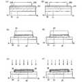
一般的な薄膜トランジスタの模式図を図22に示す。図22(A)は、薄膜トランジスタの上面図を示し、図22(B)は図22(A)のA1とB1とを結ぶ破線における断面図を示し、図22(C)は図22(A)のA2とB2とを結ぶ破線における断面図を示し、図22(D)は図22(C)の半導体層32の端部25の拡大図を示す。図22(B)〜(D)に示すように、薄膜トランジスタは、基板30上に、下地膜として機能する絶縁層31が形成され、絶縁層31上に、チャネル形成領域32a、ソース領域及びドレイン領域として機能する不純物領域32b、32cを有する半導体層32が形成され、半導体層32及び絶縁層31上にゲート絶縁膜として機能する絶縁層33が形成され、絶縁層33上にゲート電極として機能する導電層34が形成される。A schematic diagram of a general thin film transistor is shown in FIG. 22A is a top view of the thin film transistor, FIG. 22B is a cross-sectional view taken along the broken line connecting A1 and B1 in FIG. 22A, and FIG. 22C is FIG. 22A. FIG. 22D is an enlarged view of the
図22に示した薄膜トランジスタを作製する工程において、選択的にエッチングされた半導体層32上にゲート絶縁膜として機能する絶縁層33を形成する場合、半導体層32の端部25において絶縁層33の膜厚が不均一となり絶縁層33の被覆不良が生じる。絶縁層33の膜厚が薄くなった部分においては、ゲート電圧の電界強度が強くなり、薄膜トランジスタの耐圧や信頼性に悪影響を与えていた。In the process of manufacturing the thin film transistor illustrated in FIG. 22, in the case where the
また、半導体層32の端部25には、基板及び各薄膜の応力が集中するため、素子特性の変動を引き起こし問題となっていた。Further, the stress of the substrate and each thin film is concentrated on the
この半導体層32の端部の段差に起因するゲート絶縁膜の被覆性の低下を改善する手段として、活性層の端部をテーパー形状とする手段が用いられている(例えば、特許文献2)。As means for improving the decrease in coverage of the gate insulating film due to the step at the end of the
一方、高速動作を必要とする回路を構成する薄膜トランジスタとしては、チャネル長が短く、且つゲート絶縁膜の膜厚が薄いことが好ましい。このため、ゲート絶縁膜の膜厚は、数十ナノメートルと膜厚が薄くなっている。
しかしながら、半導体層の端部をテーパー形状にしても、電界や応力の集中は依然として問題となっている。However, even if the end portion of the semiconductor layer is tapered, the concentration of electric field and stress still remains a problem.
つまり、半導体層の端部をテーパー形状にしても、半導体層の端部においてゲート絶縁膜の膜厚が不均一となり、ゲート絶縁膜が薄い箇所において電界集中が生じてしまう。電界集中が起きることでリーク電流が増大し、デバイスの消費電力が増大する。更には、電界集中が過度な場合にはゲート絶縁膜の破壊が起こり、ゲートリーク不良が発生する。そのため、ゲート耐圧が低下する。これらはゲート絶縁膜の膜厚を数十ナノメートルと薄くした場合に特に顕著な問題である。That is, even if the end portion of the semiconductor layer is tapered, the thickness of the gate insulating film is not uniform at the end portion of the semiconductor layer, and electric field concentration occurs at a portion where the gate insulating film is thin. When electric field concentration occurs, the leakage current increases and the power consumption of the device increases. Furthermore, when the electric field concentration is excessive, the gate insulating film is destroyed and a gate leak defect occurs. As a result, the gate breakdown voltage decreases. These are particularly prominent problems when the thickness of the gate insulating film is reduced to several tens of nanometers.
本願発明はこのような課題を解決するための技術であり、ゲート絶縁層の膜厚が薄くなった部分、即ち、段差部におけるゲート絶縁層の膜厚の不均一による半導体装置の特性への影響を低減し、半導体装置の信頼性を向上させることを目的とする。The present invention is a technique for solving such a problem, and the influence on the characteristics of a semiconductor device due to the non-uniformity of the thickness of the gate insulating layer at the stepped portion, that is, the stepped portion. The purpose is to improve the reliability of the semiconductor device.
本発明の半導体装置は、絶縁表面上に形成される半導体層と、半導体層上に形成される第1の絶縁層と、半導体層の端部を酸素を含む雰囲気下でプラズマ処理することにより形成される第2の絶縁層と、第1の絶縁層上及び第2の絶縁層上に形成されるゲート電極と、を有する。なお、第2の絶縁層は、半導体層のチャネル形成領域と接する酸化膜である。A semiconductor device of the present invention is formed by performing plasma treatment on a semiconductor layer formed on an insulating surface, a first insulating layer formed on the semiconductor layer, and an end portion of the semiconductor layer in an atmosphere containing oxygen. A second insulating layer, and a gate electrode formed on the first insulating layer and the second insulating layer. Note that the second insulating layer is an oxide film in contact with the channel formation region of the semiconductor layer.
また、本発明の半導体装置は、絶縁表面上に半導体層を形成し、半導体層上に第1の絶縁層を形成し、半導体層及び第1の絶縁層をエッチングして半導体層の端部を露出させ、酸素を含む雰囲気下で半導体層の露出した部分をプラズマ処理して第2の絶縁層を形成し、前記第1の絶縁層上及び前記第2の絶縁層上にゲート電極を形成することで作製することができる。In the semiconductor device of the present invention, a semiconductor layer is formed over an insulating surface, a first insulating layer is formed over the semiconductor layer, and the semiconductor layer and the first insulating layer are etched so that an end portion of the semiconductor layer is formed. The exposed portion of the semiconductor layer is exposed to plasma in an atmosphere containing oxygen to form a second insulating layer, and a gate electrode is formed on the first insulating layer and the second insulating layer. Can be produced.
また、プラズマ処理は、電子密度が1×1011cm−3以上1×1013cm−3以下で、電子温度が0.5eV以上1.5eV以下のプラズマを用いて行うことができる。プラズマ処理は例えば、酸素と希ガスとの混合ガス雰囲気下、酸素と水素と希ガスとの混合ガス雰囲気下、一酸化二窒素と希ガスとの混合ガス雰囲気下、または一酸化二窒素と水素と希ガスとの混合ガス雰囲気下で行うことができる。The plasma treatment can be performed using plasma with an electron density of 1 × 10¹¹
本発明において、ゲート電極下の半導体層のチャネル形成領域の端部(側面)に絶縁層を有するため、ゲート絶縁膜の半導体層表面への被覆不良が半導体装置に及ぼす影響を低減することができる。つまり、半導体層のチャネル形成領域の側面とゲート電極とが接するのを防ぐことができる。In the present invention, since the insulating layer is provided at the end (side surface) of the channel formation region of the semiconductor layer under the gate electrode, it is possible to reduce the influence of the poor coating on the semiconductor layer surface of the gate insulating film on the semiconductor device. . That is, the side surface of the channel formation region of the semiconductor layer can be prevented from contacting the gate electrode.
また、ゲート絶縁層の実効膜厚に比べて半導体層の端部に形成される酸化膜の実効膜厚を厚くすることができるため、半導体層の端部における電界集中を緩和することができる。In addition, since the effective thickness of the oxide film formed at the end portion of the semiconductor layer can be increased compared to the effective thickness of the gate insulating layer, electric field concentration at the end portion of the semiconductor layer can be reduced.
また、半導体層の端部と下地膜として機能する絶縁層との接する部分において絶縁層に凹部が形成される場合があるが、半導体層の端部に選択的に絶縁層を形成することができるため、下地の絶縁層に凹部が形成されても、半導体層とゲート電極とが接することがなくなる。In addition, a recess may be formed in the insulating layer in a portion where the end portion of the semiconductor layer is in contact with the insulating layer functioning as a base film, but the insulating layer can be selectively formed in the end portion of the semiconductor layer. Therefore, even when a recess is formed in the base insulating layer, the semiconductor layer and the gate electrode are not in contact with each other.
従って、ゲートリーク不良を低減し、ゲート電極の耐圧を向上させることが可能となる。本発明は、ゲート絶縁層として機能する絶縁膜の膜厚が数ナノメートル〜数十ナノメートルのように、膜厚が半導体層の膜厚よりも薄い場合に特に効果的である。従って、信頼性が高い半導体装置を作製することができる。Therefore, it is possible to reduce gate leakage defects and improve the breakdown voltage of the gate electrode. The present invention is particularly effective when the thickness of the insulating film functioning as the gate insulating layer is smaller than the thickness of the semiconductor layer, such as several nanometers to several tens of nanometers. Therefore, a highly reliable semiconductor device can be manufactured.
本発明の実施の形態について、図面を用いて以下に説明する。但し、本発明は以下の説明に限定されず、本発明の趣旨及びその範囲から逸脱することなくその形態及び詳細を様々に変更し得ることは当業者であれば容易に理解される。従って、本発明は以下に示す実施の形態の記載内容に限定して解釈されるものではない。なお、以下に説明する本発明の構成において、同じものを指す符号は異なる図面間で共通して用いる場合がある。Embodiments of the present invention will be described below with reference to the drawings. However, the present invention is not limited to the following description, and it is easily understood by those skilled in the art that modes and details can be variously changed without departing from the spirit and scope of the present invention. Therefore, the present invention should not be construed as being limited to the description of the embodiments below. Note that in the structures of the present invention described below, the same reference numerals may be used in common in different drawings.
(実施の形態1)
本実施の形態では、半導体層の端部におけるゲート絶縁膜の被覆不良によるリーク電流を抑制することが可能な半導体装置の構造について説明する。(Embodiment 1)
In this embodiment mode, a structure of a semiconductor device capable of suppressing leakage current due to poor coverage of a gate insulating film at an end portion of a semiconductor layer will be described.
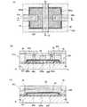
図1は本発明に係る半導体装置の主要な構成を説明するための上面図及び断面図である。図1(A)は、特に薄膜トランジスタの要部の上面図を示し、図1(B)は図1(A)のA1とB1とを結ぶ破線における断面図を示し、図1(C)は図1(A)のA2とB2とを結ぶ破線における断面図を示している。1A and 1B are a top view and a cross-sectional view for explaining a main configuration of a semiconductor device according to the present invention. 1A shows a top view of a main portion of the thin film transistor, and FIG. 1B shows a cross-sectional view taken along a broken line connecting A1 and B1 in FIG. 1A. Shows a cross-sectional view taken along a broken line connecting A2 and B2 in FIG.
本実施の形態に示す薄膜トランジスタは、基板30上に絶縁層31を介して島状に設けられた半導体層32と、半導体層32上に形成されたゲート絶縁層33と、半導体層32の上方にゲート絶縁層33を介して設けられたゲート電極として機能する導電層34と、を含む薄膜トランジスタ205と、ゲート絶縁層33及び導電層34を覆って設けられた絶縁層203と、絶縁層203上に設けられたソース電極又はドレイン電極として機能する導電層204とを有している(図1(A)〜(C))。なお、半導体層32は、チャネル形成領域32aとソース領域又はドレイン領域として機能する不純物領域32b、32cとに加えて、半導体層32の端部、ここでは導電層34の下方のチャネル形成領域32aに接した部分に形成された絶縁層36とを有している。なお、チャネル形成領域32a中に、不純物領域32b、32cに添加した不純物とは逆の導電型の不純物が添加されていてもよい。The thin film transistor described in this embodiment includes a
ここで、絶縁層36は、酸素を含む雰囲気下で半導体層32の端部をプラズマ処理することにより形成された酸化膜である。半導体層の端部に形成された絶縁層36は、半導体層32の端部とゲート電極として機能する導電層34が短絡してリーク電流が流れるのを防止するために設ける。従って、絶縁層36は、少なくとも半導体層32のチャネル形成領域32aの側面(露出している部分)に形成されていればよい。ただし、それ以外の部分に形成されていてももちろん構わない。なお、本実施の形態において、絶縁層36はゲート絶縁層33の下側(基板側)の領域にゲート絶縁層33と接して形成されている。Here, the insulating
本実施の形態において、基板30上に形成された絶縁層31上に、半導体層とゲート絶縁層として機能する絶縁層とを順次形成し、半導体層と絶縁層とをエッチングすることにより、島状に設けられた半導体層32及びゲート絶縁層33を形成する。その後、ゲート絶縁層33及び半導体層32の端部の半導体層が露出している部分に対してプラズマ処理を行うことにより、半導体層32の端部に絶縁層36を形成することができる。In this embodiment mode, a semiconductor layer and an insulating layer functioning as a gate insulating layer are sequentially formed over the insulating
なお、本実施の形態において、ゲート絶縁層33の表面からプラズマ処理を行うため、半導体層32の端部のみではなく、ゲート絶縁層33と接する半導体層32表面も酸化される。従って、ゲート絶縁層33と接する半導体層32表面にも絶縁層36が形成されている。Note that in this embodiment mode, plasma treatment is performed from the surface of the
本実施の形態に示す半導体装置は、ゲート電極下の半導体層のチャネル形成領域の端部(側面)に絶縁層を有するため、ゲート絶縁膜の半導体層表面への被覆不良が半導体装置に及ぼす影響を低減することができる。つまり、半導体層のチャネル形成領域の側面とゲート電極とが接しない構造にできるため、ゲートリーク不良を低減し、ゲート電極の耐圧を向上させることが可能となる。Since the semiconductor device described in this embodiment includes an insulating layer at the end (side surface) of the channel formation region of the semiconductor layer under the gate electrode, the influence of the poor coating of the gate insulating film on the surface of the semiconductor layer on the semiconductor device Can be reduced. In other words, since the side surface of the channel formation region of the semiconductor layer and the gate electrode can be prevented from being in contact with each other, gate leakage defects can be reduced and the breakdown voltage of the gate electrode can be improved.
本実施の形態において、ゲート絶縁層33は、酸化シリコン(SiO)膜、窒化シリコン(SiN)膜、酸化窒化シリコン(SiOxNy)(x>y>0)膜、窒化酸化シリコン(SiNxOy)(x>y>0)膜、Hf系酸化膜等を単層又は積層した膜を用いて形成することができる。このような絶縁層は、気相成長法やスパッタリング法で形成することができる。なお、気相成長法やスパッタリング法で形成されたゲート絶縁膜表面をプラズマ処理してもよい。また、半導体層32を形成した後に、酸素を含む雰囲気又は窒素を含む雰囲気下で半導体膜表面をプラズマ処理することにより、半導体膜表面に形成された酸化シリコン(SiO)膜、窒化シリコン(SiN)膜、酸化窒化シリコン(SiOxNy)(x>y>0)膜、又は窒化酸化シリコン(SiNxOy)(x>y>0)膜をゲート絶縁層として用いることもできる。In this embodiment, the
ここで、ゲート絶縁層33として、酸化シリコン(SiO)膜、窒化シリコン(SiN)膜、酸化窒化シリコン(SiOxNy)(x>y>0)膜、窒化酸化シリコン(SiNxOy)(x>y>0)膜、Hf系酸化膜等を単層又は積層した膜を、気相成長法やスパッタリング法を用いて形成する場合、これらの膜の誘電率に比べて半導体層32の端部に形成される酸化膜の誘電率は小さくなる。よって、ゲート絶縁層33と半導体層の端部に形成される絶縁層36とを同程度の膜厚で形成した場合でも、ゲート絶縁層33の実効膜厚に比べて半導体層32の端部に形成される絶縁層36(酸化膜)の実効膜厚を厚くすることができ、半導体層32の端部における電界集中を緩和することができる。例えば、ゲート絶縁層33を5〜20nm程度の膜厚で形成した場合、ゲート絶縁層33の実効膜厚に比べて半導体層32の端部に形成される酸化膜の実効膜厚は厚くなり、半導体層32の端部における電界集中を緩和することができる。従って、ゲートリーク不良を低減し、ゲート電極の耐圧を向上させることが可能となる。Here, as the
また、ゲート絶縁層33として窒化シリコン(SiN)膜や窒化酸化シリコン(SiNxOy)(x>y>0)膜を用いた場合、ゲート絶縁層33に接する半導体層32の酸化速度に比べて、半導体層32の端部の露出している部分の酸化速度が速いため、半導体層32の端部に厚く酸化膜を形成することができる。よって、半導体層32の端部付近における電界集中を緩和することができ、ゲートリーク不良を低減し、ゲート電極の耐圧を向上させることが可能となる。Further, when a silicon nitride (SiN) film or a silicon nitride oxide (SiNxOy) (x> y> 0) film is used as the
また、エッチングして半導体層32及び絶縁層33を形成する際に、図2(A)に示すように、半導体層32の下地膜として形成される絶縁層31も部分的に除去され、窪み37が形成されることがある。窪み37が形成された場合に、半導体層32上にゲート絶縁層33を形成すると、半導体層32及び窪み37の段差を覆いきれず、ゲート絶縁層33が部分的に切断されてしまい、半導体層32とゲート電極として機能する導電層34とが接して半導体層32及びゲート電極層の間でリーク電流が生じてしまう可能性がある。Further, when the
しかしながら本実施の形態で示すように、島状の半導体層32とゲート絶縁層33を形成した後に半導体層32表面を酸素を含む雰囲気下でプラズマ処理して半導体層32の端部に絶縁層36を形成することにより、図2(B)に示すように半導体層32の表面を絶縁層で覆うことができる。従って、絶縁層31が部分的に除去されて窪み37が形成された場合でも、半導体層32のチャネル形成領域32aと半導体層32上に形成される導電層34とが接することがなくなる。従って、ゲートリーク不良を低減し、ゲート電極の耐圧を向上させることが可能となる。However, as shown in this embodiment mode, after the island-shaped
なお、酸素を含む雰囲気下として例えば、酸素(O2)と希ガス(He、Ne、Ar、Kr、Xeの少なくとも一つを含む)との混合ガス雰囲気下、酸素と水素(H2)と希ガスとの混合ガス雰囲気下、一酸化二窒素と希ガスとの混合ガス雰囲気下、または一酸化二窒素と水素と希ガスとの混合ガス雰囲気下で行うことができる。例えば、酸素(O2)、水素(H2)とアルゴン(Ar)との混合ガスを用いることができる。その場合、酸素を0.1〜100sccm、水素を0.1〜100sccm、アルゴンを100〜5000sccm含んだ混合ガスを用いることができる。なお、酸素:水素:アルゴン=1:1:100の比率で混合ガスを導入することが好ましい。例えば、酸素を5sccm、水素を5sccm、アルゴンを500sccmとして導入すればよい。Note that as an atmosphere containing oxygen, for example, oxygen and hydrogen (H2 ) are mixed in an atmosphere of mixed gas of oxygen (O2 ) and a rare gas (including at least one of He, Ne, Ar, Kr, and Xe). The reaction can be performed in a mixed gas atmosphere of a rare gas, a mixed gas atmosphere of dinitrogen monoxide and a rare gas, or a mixed gas atmosphere of dinitrogen monoxide, hydrogen, and a rare gas. For example, a mixed gas of oxygen (O2 ), hydrogen (H2 ), and argon (Ar) can be used. In that case, a mixed gas containing 0.1 to 100 sccm of oxygen, 0.1 to 100 sccm of hydrogen, and 100 to 5000 sccm of argon can be used. Note that the mixed gas is preferably introduced at a ratio of oxygen: hydrogen: argon = 1: 1: 100. For example, oxygen may be introduced at 5 sccm, hydrogen at 5 sccm, and argon at 500 sccm.
また、窒素を含む雰囲気下として例えば、窒素(N2)と希ガス(He、Ne、Ar、Kr、Xeの少なくとも一つを含む)との混合ガス雰囲気下、窒素と水素と希ガスとの混合ガス雰囲気下、またはアンモニア(NH3)と希ガスとの混合ガス雰囲気下で行うことができる。Further, as an atmosphere containing nitrogen, for example, in a mixed gas atmosphere of nitrogen (N2 ) and a rare gas (including at least one of He, Ne, Ar, Kr, and Xe), nitrogen, hydrogen, and a rare gas The reaction can be performed in a mixed gas atmosphere or a mixed gas atmosphere of ammonia (NH3 ) and a rare gas.
なお、プラズマ処理は、上記ガスの雰囲気中において、電子密度が1×1011cm−3以上であり、電子温度が1.5eV以下のプラズマを用いて行う。より詳しくいうと、電子密度が1×1011cm−3以上1×1013cm−3以下で、電子温度が0.5eV以上1.5eV以下のプラズマで行う。上記プラズマはプラズマの電子密度が高密度であり、基板30上に形成された被処理物(ここでは、半導体層32)付近での電子温度が低いため、被処理物に対するプラズマによる損傷を防止することができる。また、プラズマの電子密度が1×1011cm−3以上と高密度であるため、プラズマ処理を用いて、被照射物を酸化することよって形成される酸化物または窒化膜は、CVD法やスパッタ法等により形成された膜と比較して膜厚等が均一性に優れ、且つ緻密な膜を形成することができる。また、プラズマの電子温度が1.5eV以下と低いため、従来のプラズマ処理や熱酸化法と比較して低い温度で酸化または窒化処理を行うことができる。例えば、ガラス基板の歪点よりも100度以上低い温度でプラズマ処理を行っても十分に酸化を行うことができる。また、プラズマを形成するための周波数としては、マイクロ波(2.45GHz)等の高周波を用いることができる。Note that the plasma treatment is performed using plasma with an electron density of 1 × 1011 cm−3 or more and an electron temperature of 1.5 eV or less in the atmosphere of the gas. More specifically, plasma is used with an electron density of 1 × 10¹¹
なお、薄膜トランジスタの形状は図1に示すものに限られるものではなく、例えばゲート電極として機能する導電層34の側壁に接して絶縁物からなるサイドウォール301を形成してもよいし、ソース領域又はドレイン領域として機能する不純物領域32b、32cとチャネル形成領域32aとの間に、不純物領域32b、32cより低濃度に不純物が添加された低濃度不純物領域(LDD領域)32d、32eが形成されていてもよい(図9(A))。また、薄膜トランジスタの構造として上述した構造に限られず、チャネル形成領域が1つ形成されるシングルゲート構造でもよいし、2つ形成されるダブルゲート構造または3つ形成されるトリプルゲート構造等のマルチゲート構造を用いることができる。また、ゲート電極を積層構造で設けてもよい。例えば、ゲート電極を第1の導電層34aと第1の導電層34a上に形成される第2の導電層34bとの2層構造とし、第1の導電膜をテーパー状で形成し、第1の導電膜にのみ重なるように低濃度不純物領域32d、32eを設ける構造(図9(B))としてもよい。また、ゲート電極を第1の導電層34aと第1の導電層34a上に形成される第2の導電層34bで設け、第2の導電層34bの側壁に接し且つ導電層34aの上方に形成されるようにサイドウォール301を設ける構造(図9(C))としてもよい。また、ソース領域またはドレイン領域として機能する不純物領域32b、32cをNi、Co、W等のシリサイドで形成することも可能である。Note that the shape of the thin film transistor is not limited to that illustrated in FIG. 1. For example, the
(実施の形態2)
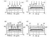
本実施の形態では、図1に示した半導体装置の作製方法の一例に関して図面を参照して説明する。なお、本実施の形態では図1(A)のA1とB1とを結ぶ破線での断面における作製工程を図3(A)〜(C)、図4(A)〜(B)を用いて、図1(A)のA2とB2とを結ぶ破線での断面における作製工程を図3(D)〜(F)、図4(C)〜(D)を用いて説明する。(Embodiment 2)
In this embodiment, an example of a method for manufacturing the semiconductor device illustrated in FIG. 1 will be described with reference to drawings. Note that in this embodiment mode, a manufacturing process in a cross-sectional view taken along a broken line connecting A1 and B1 in FIG. 1A is used with reference to FIGS. 3A to 3C and FIGS. A manufacturing process in a cross section taken along a broken line connecting A2 and B2 in FIG. 1A will be described with reference to FIGS. 3D to 3F and FIGS.
まず、基板30上に絶縁層31を形成する(図3(A)、(D))。First, the insulating
基板30は、ガラス基板、石英基板、金属基板(例えばセラミック基板またはステンレス基板など)、Si基板等の半導体基板などを用いることができる。また、他にもプラスチック基板として、ポリエチレンテレフタレート(PET)、ポリエチレンナフタレート(PEN)、ポリエーテルサルフィン(PES)、アクリルなどの基板を選択することもできる。As the
絶縁層31は、基板30からアルカリ金属などの不純物が拡散して、上に形成される素子の汚染を防ぐものであり、ブロッキング層として適宜設ければ良い。例えば、CVD法やスパッタリング法等を用いて、酸化シリコン、窒化シリコン、酸化窒化シリコン(SiOxNy)(x>y>0)、窒化酸化シリコン(SiNxOy)(x>y>0)等の絶縁材料を用いて形成することができる。例えば、絶縁層31を2層構造とする場合、第1層目の絶縁膜として窒化酸化シリコン膜を形成し、第2層目の絶縁膜として酸化窒化シリコン膜を形成するとよい。また、第1層目の絶縁膜として窒化シリコン膜を形成し、第2層目の絶縁膜として酸化シリコン膜を形成してもよい。The insulating
続いて、絶縁層31上に半導体膜201を形成する。半導体膜201は、非晶質半導体膜又は結晶質半導体膜で形成することができる。結晶性半導体膜としては、絶縁層31上に形成した非晶質半導体膜を熱処理やレーザー光の照射によって結晶化させたものなどを用いることができる。なお、半導体材料としては、シリコンが好ましく、その他にシリコンゲルマニウム半導体等を用いることもできる。Subsequently, a
半導体膜201は、10nm〜200nm、好ましくは10nm〜50nm程度、更に好ましくは10nm〜30nm程度の膜厚で形成するとよい。なお、50nm以下の半導体膜を形成する場合、50nm以上の膜厚で半導体膜を形成した後で、半導体膜の表面をドライエッチング処理することにより10nm〜50nm程度の膜厚の半導体膜を形成してもよい。このときのエッチングの際のエッチングガスとしては、Cl2、BCl3、SiCl4等の塩素系のガス、CF4、NF3、SF6、CHF3、CF4等のフッ素系のガス、又はフッ素系ガスにO2ガス、H2ガス、HeやAr等の不活性ガスを適宜加えた混合ガス等を用いることができる。なお、ドライエッチングの前に、半導体膜表面を希フッ酸処理して半導体表面に形成される自然酸化膜を除去し、その後半導体表面をオゾン水などで処理して半導体表面に酸化膜を形成しておいてもよい。The
半導体膜201を50nm以下程度の薄膜で形成することにより、半導体膜表面に形成されるゲート絶縁層の被覆不良を低減することができる。また、半導体膜を薄膜で形成することにより、TFTをより小型化することができる。また、TFTのしきい値電圧を小さくするためにチャネル形成領域への不純物元素のドープ量を増加させた場合でも、半導体膜を薄膜で形成することにより完全空乏型のTFTを作製しやすくなるため、良好なS値でしきい値電圧の小さなTFTを作製することができる。By forming the
また、非結晶半導体膜をレーザー光の照射によって結晶化若しくは再結晶化した膜を半導体膜201として用いる場合、レーザー光の光源としてLD励起の連続発振(CW)レーザー(YVO4、第2高調波(波長532nm))を用いることができる。特に第2高調波に限定する必要はないが、第2高調波はエネルギー効率の点で、さらに高次の高調波より優れている。CWレーザーを半導体膜に照射すると、連続的に半導体膜にエネルギーが与えられるため、一旦半導体膜を溶融状態にすると、溶融状態を継続させることができる。さらに、CWレーザーを走査することによって半導体膜の固液界面を移動させ、この移動の方向に沿って一方向に長い結晶粒を形成することができる。また、固体レーザーを用いるのは、気体レーザー等と比較して、出力の安定性が高く、安定した処理が見込まれるためである。なお、CWレーザーに限らず、繰り返し周波数が10MHz以上のパルスレーザを用いることも可能である。繰り返し周波数が高いパルスレーザを用いると、半導体膜が溶融してから固化するまでの時間よりもレーザーのパルス間隔が短ければ、常に半導体膜を溶融状態にとどめることができ、固液界面の移動により一方向に長い結晶粒で構成される半導体膜を形成することができる。その他のCWレーザー及び繰り返し周波数が10MHz以上のパルスレーザを使用することもできる。例えば、気体レーザーとしては、Arレーザー、Krレーザー、CO2レーザー等がある。固体レーザーとして、YAGレーザー、YLFレーザー、YAlO3レーザー、GdVO4レーザー、KGWレーザー、KYWレーザー、アレキサンドライトレーザー、Ti:サファイアレーザー、Y2O3レーザー、YVO4レーザー等がある。また、YAGレーザー、Y2O3レーザー、GdVO4レーザー、YVO4レーザーなどのセラミックスレーザがある。金属蒸気レーザーとしてはヘリウムカドミウムレーザ等が挙げられる。また、レーザー発振器において、レーザー光をTEM00(シングル横モード)で発振して射出すると、被照射面において得られる線状のビームスポットのエネルギー均一性を上げることができるので好ましい。その他にも、パルス発振のエキシマレーザーを用いても良い。In the case where a film obtained by crystallizing or recrystallizing an amorphous semiconductor film by laser light irradiation is used as the
続いて、半導体膜201上にゲート絶縁層として機能する絶縁層206を形成する(図3(A)、(D))。絶縁層206は、酸化シリコン膜、窒化シリコン膜、酸化窒化シリコン(SiOxNy)(x>y>0)膜、窒化酸化シリコン(SiNxOy)(x>y>0)膜、Hf系酸化膜等を用いて形成することができる。このような絶縁層は、気相成長法やスパッタリング法で形成することができる。また、半導体層201表面を酸素を含む雰囲気下又は窒素を含む雰囲気下でプラズマ処理することにより形成することもできる。Subsequently, an insulating
次に、絶縁層206上にレジスト202を選択的に形成する(図3(A)、(D))。そして、レジスト202をマスクとして絶縁層206及び半導体膜201をドライエッチングして、ゲート絶縁層33及び島状の半導体層32を形成する(図3(B)、(E))。なお、レジスト202は、エッチングの際のマスクとして用いるものであり、ポジ型のフォトレジストやネガ型のフォトレジスト等を適宜選択して用いることができる。Next, a resist 202 is selectively formed over the insulating layer 206 (FIGS. 3A and 3D). Then, the insulating
なお、ドライエッチングのときのエッチングガスとしては、CF4、NF3、SF6、CHF3、CF4等のフッ素系のガス、又は該フッ素系ガスにO2ガス、H2ガス、HeやAr等の不活性ガスを適宜加えた混合ガス等を用いることができる。好ましくは、CF4とO2との混合ガス、SF6とO2との混合ガス、CHF3とHeとの混合ガス、又はCF4とH2との混合ガスを用いるとよい。また、エッチングはドライエッチングに限られずウェットエッチングで行ってもよい。その場合、半導体膜201に対してTMAH(tetramethylanmmonium hydroxide、テトラメチルアンモニウムヒドロキシド)に代表される有機アルカリ系水溶液を用いたウェットエッチングを行うことにより島状の半導体層32を形成することができる。なお、エッチング液としてTMAH等を用いた場合、半導体膜201のみが選択的にエッチングされるため、下地の絶縁層31にダメージを与えずにエッチングすることができる。このように、絶縁表面に形成された半導体層を島状に分離形成することで、同一基板上に複数の薄膜トランジスタと周辺回路を形成した場合に、それぞれの素子を分離をすることができる。すなわち、10V〜20V程度の電圧で書き込みや消去を行う必要のあるメモリ素子アレイと、3V〜7V程度の電圧で動作してデータの入出力や命令の制御を主として行う周辺回路を同一基板上に形成した場合でも、各素子に印加する電圧の違いによる相互の干渉を防ぐことができる。As an etching gas at the time of dry etching, a fluorine-based gas such as CF4 , NF3 , SF6 , CHF3 , CF4 , or the fluorine-based gas includes O2 gas, H2 gas, He, and Ar. A mixed gas or the like to which an inert gas such as the above is appropriately added can be used. Preferably, a mixed gas of CF4 and O2 , a mixed gas of SF6 and O2 , a mixed gas of CHF3 and He, or a mixed gas of CF4 and H2 may be used. Etching is not limited to dry etching, and may be performed by wet etching. In that case, the island-shaped
また、島状の半導体層32の端部の断面形状は必ずしもテーパー状になっている必要はない。半導体層の端部付近に形成される膜の被覆不良の低減を考慮すると、よりθの角度が小さいほうが好ましいが、θが45°〜95°程度のテーパー状や垂直形状にエッチングしてもよい。Further, the cross-sectional shape of the end portion of the island-shaped
続いて、ゲート絶縁層33上に形成されたレジスト202を除去する。そして、酸素を含む雰囲気中でプラズマ処理することにより、半導体層32の端部及びゲート絶縁層33と接する半導体層32の表面に絶縁層36を形成する(図3(C)、(F))。Subsequently, the resist 202 formed on the
次に、ゲート絶縁層33上にゲート電極として機能する導電層34を形成する(図4(A)、(C))。ここでは、導電層34は単層で形成した例を示しているが、もちろん導電性材料を2層又は3層以上の積層で設けた構造としてもよい。なお、ここでは図示しないが、導電層34は、ゲート絶縁層33上を覆って形成された導電層を選択的にエッチングすることにより形成することができる。Next, a
また、導電層34は、タンタル(Ta)、タングステン(W)、チタン(Ti)、モリブデン(Mo)、アルミニウム(Al)、銅(Cu)、クロム(Cr)、ニオブ(Nb)等から選択された元素またはこれらの元素を主成分とする合金材料若しくは化合物材料で形成することができる。また、リン等の不純物元素をドーピングした多結晶珪素に代表される半導体材料により形成することもできる。例えば、導電層34を第1の導電膜と第2の導電膜との積層構造とする場合、第1の導電膜として窒化タンタルを用い、第2の導電膜としてタングステンを用いて形成するとよい。なお、この組み合わせに限られず、導電層34を積層して形成する場合には、上記材料を自由に組み合わせて設けることができる。The
続いて、導電層34をマスクとして半導体層32に不純物元素121を導入することによって、半導体層32に不純物領域32b、32c及び不純物元素121が導入されないチャネル形成領域32aを形成する(図4(A)、(C))。なお、ここでは、導電層34を島状の半導体層32を横断するように形成した後に不純物元素を導入するため、導電層34に覆われていない半導体層32の領域に不純物が導入されて不純物領域32b、32cが形成され、導電層34に覆われた半導体層32の領域には不純物元素121が導入されないチャネル形成領域32aが形成される。Subsequently, by introducing the
ここで、不純物元素121としては、n型を付与する不純物元素又はp型を付与する不純物元素を用いることができる。n型を示す不純物元素としては、リン(P)やヒ素(As)等を用いることができる。p型を示す不純物元素としては、ボロン(B)やアルミニウム(Al)やガリウム(Ga)等を用いることができる。例えば、不純物元素121として、リン(P)を1×10¹⁸〜1×10²¹/cm3の濃度で含まれるように半導体層32に導入し、n型を示す不純物領域32b、32cを形成すればよい。なお、チャネル形成領域32aとソース領域又はドレイン領域との間に、ソース領域又はドレイン領域より低濃度に不純物が添加された低濃度不純物領域(LDD領域)を形成してもよい。低濃度不純物領域を設けることにより、ドレイン端の電界を緩和して、書き込み及び消去の繰り返しによる劣化を抑制することができる。Here, as the
また、チャネル形成領域32a中に、不純物領域32b、32cに添加した不純物とは逆の導電型を有する不純物元素(例えばn型TFTに対してはボロン)を添加してもよい。チャネル形成領域32a中に逆導電型の不純物を添加することにより、TFTのしきい値電圧を制御することができる。なお、この不純物元素はゲート電極を介してドープすることによって添加してもよいし、ゲート電極形成前に予め添加しておいてもよい。Further, an impurity element having a conductivity type opposite to that of the impurity added to the
次に、導電層34、ゲート絶縁層33、絶縁層31等を覆うように絶縁層203を形成する(図4(B)、(D))。その後、ゲート絶縁層33及び絶縁層203にコンタクトホールを形成し、絶縁層203上にソース電極又はドレイン電極として機能する導電層204を選択的に形成する(図4(B)、(D))。ここで、導電層204は、半導体層32のソース領域又はドレイン領域として機能する不純物領域32b、32cと電気的に接続されるように設ける。Next, the insulating
ここで、絶縁層203は、CVD法やスパッタリング法等で形成した、酸化シリコン、酸化窒化シリコン(SiOxNy)(x>y>0)、窒化酸化シリコン(SiNxOy)(x>y>0)などを用いることができる。また、ポリイミド、ポリアミド、ポリビニルフェノール、ベンゾシクロブテン、アクリル、エポキシ等の有機材料、またはシロキサン樹脂等のシロキサン材料、オキサゾール樹脂などからなる単層または積層構造で設けることができる。なお、シロキサン材料とは、Si−O−Si結合を含む材料に相当する。シロキサンは、シリコン(Si)と酸素(O)との結合で骨格構造が構成される。置換基として、少なくとも水素を含む有機基(例えばアルキル基、芳香族炭化水素)が用いられる。置換基として、フルオロ基を用いることもできる。オキサゾール樹脂は、例えば、感光性ポリベンゾオキサゾール等である。感光性ポリベンゾオキサゾールは、誘電率が低く(常温1MHzで誘電率2.9)、耐熱性が高く(示差熱天秤(TGA:thermal gravity analysis)昇温5℃/minで熱分解温度550℃)、吸水率が低い(常温24時間で0.3%)材料である。オキサゾール樹脂は、ポリイミド等の比誘電率(3.2〜3.4程度)と比較すると、比誘電率が低いため(2.9程度)、寄生容量の発生を抑制し、高速動作を行うことができる。ここでは、絶縁層203として、CVD法で形成した酸化シリコン、酸化窒化シリコン(SiOxNy)(x>y>0)又は窒化酸化シリコン(SiNxOy)(x>y>0)を単層又は積層して形成する。また、さらに、ポリイミド、ポリアミド、ポリビニルフェノール、ベンゾシクロブテン、アクリル、エポキシ等の有機材料、シロキサン樹脂等のシロキサン材料、又はオキサゾール樹脂を積層して形成してもよい。Here, the insulating
また、導電層204は、アルミニウム、タングステン、チタン、タンタル、モリブデン、ニッケル、ネオジウムから選ばれた一種の元素または当該元素を複数含む合金からなる単層構造または積層構造を用いることができる。例えば、当該元素を複数含む合金からなる導電膜として、チタンを含有したアルミニウム合金、ネオジウムを含有したアルミニウム合金などで形成することができる。また、積層構造で設ける場合、例えば、アルミニウム層若しくは前記したようなアルミニウム合金層を、チタン層で挟んで積層させた構造としても良い。The
以上の工程により、薄膜トランジスタ205を含む半導体装置を作製することができる。Through the above steps, a semiconductor device including the
本実施の形態に示す半導体装置の作製工程を用いることにより、ゲート電極下の半導体層のチャネル形成領域の端部(側面)に絶縁層を有する半導体装置を作製することができる。従って、ゲート絶縁膜の半導体層表面への被覆不良が半導体装置に及ぼす影響を低減することができる。つまり、本実施の形態の方法を用いて作製された半導体装置は、半導体層のチャネル形成領域の側面はゲート電極と接することがなくなるため、ゲートリーク不良を低減し、ゲート電極の耐圧を向上させることが可能となる。By using the manufacturing process of the semiconductor device described in this embodiment, a semiconductor device having an insulating layer at an end portion (side surface) of the channel formation region of the semiconductor layer under the gate electrode can be manufactured. Accordingly, it is possible to reduce the influence on the semiconductor device due to the poor coating of the gate insulating film on the surface of the semiconductor layer. That is, in the semiconductor device manufactured using the method of this embodiment, the side surface of the channel formation region of the semiconductor layer is not in contact with the gate electrode, so that gate leakage defects are reduced and the breakdown voltage of the gate electrode is improved. It becomes possible.
また、半導体層のチャネル形成領域の端部に選択的に厚く絶縁層を設けることができるため、半導体層のチャネル形成領域の端部における電界集中を緩和することができる。従って、ゲートリーク不良を低減し、ゲート電極の耐圧を向上させることが可能となる。In addition, since the insulating layer can be selectively provided thick at the end of the channel formation region of the semiconductor layer, electric field concentration at the end of the channel formation region of the semiconductor layer can be reduced. Therefore, it is possible to reduce gate leakage defects and improve the breakdown voltage of the gate electrode.
(実施の形態3)
本実施の形態では、図1に示す半導体装置の作製方法について実施の形態2とは異なる方法について説明する。本実施の形態では図1(A)のA1とB1とを結ぶ破線での断面における作製工程を図5(A)〜(B)を用いて、図1(A)のA2とB2とを結ぶ破線での断面における作製工程を図5(C)〜(D)を用いて説明する。(Embodiment 3)
In this embodiment, a method for manufacturing the semiconductor device illustrated in FIGS. 1A to 1C is different from that in
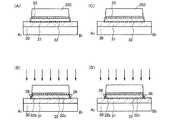
まず、実施の形態2と同様に、基板30上に絶縁層31を形成し、絶縁層31上に半導体層32及びゲート絶縁層33を形成する(図5(A)、(D))。ここで、ゲート絶縁層33上にはレジスト202が形成されている。First, as in
続いて、半導体層32及びゲート絶縁層をエッチングする際に使用したレジスト202を除去する前に、プラズマ処理を行い、半導体層32の端部を選択的に酸化する。プラズマ処理することにより、半導体層32の端部に絶縁層36を形成することができる(図5(B)、(E))。本実施の形態では、レジスト202を除去する前にプラズマ処理を行っているため、半導体層32の端部のみを選択的に酸化することが可能である。よって、絶縁層33に接する半導体層32上が酸化されることがなく、絶縁層33の実効膜厚に比べて半導体層32の端部に形成される絶縁層36の実効膜厚を厚くすることができる。従って、半導体層32の端部付近における電界集中を緩和することができ、ゲートリーク不良を低減し、ゲート電極の耐圧を向上させることが可能となる。なお、本実施の形態において、レジストの耐熱温度以下でプラズマ処理を行うことが好ましい。Subsequently, before the resist 202 used for etching the
続いて、レジスト202を除去する。以降の工程は、実施の形態2と同様に行うことによって図1に示す半導体装置を作製することができる。Subsequently, the resist 202 is removed. The subsequent steps are performed in the same manner as in
本実施の形態に示す半導体装置の作製工程を用いることにより、ゲート電極下の半導体層のチャネル形成領域の端部(側面)に絶縁層を有する半導体装置を作製することができる。従って、ゲート絶縁膜の半導体層表面への被覆不良が半導体装置に及ぼす影響を低減することができる。つまり、本実施の形態の方法を用いて作製された半導体装置は、半導体層のチャネル形成領域の側面はゲート電極と接することがなくなる、ゲートリーク不良を低減し、ゲート電極の耐圧を向上させることが可能となる。By using the manufacturing process of the semiconductor device described in this embodiment, a semiconductor device having an insulating layer at an end portion (side surface) of the channel formation region of the semiconductor layer under the gate electrode can be manufactured. Accordingly, it is possible to reduce the influence on the semiconductor device due to the poor coating of the gate insulating film on the surface of the semiconductor layer. That is, in the semiconductor device manufactured using the method of this embodiment, the side surface of the channel formation region of the semiconductor layer is not in contact with the gate electrode, the gate leakage defect is reduced, and the breakdown voltage of the gate electrode is improved. Is possible.
また、半導体層のチャネル形成領域の端部に選択的に厚く絶縁層を設けることができるため、半導体層のチャネル形成領域の端部における電界集中を緩和することができる。従って、ゲートリーク不良を低減し、ゲート電極の耐圧を向上させることが可能となる。
(実施の形態4)
本実施の形態では、単結晶シリコン基板上に酸化シリコンでなる酸化膜を形成し、酸化膜上に形成された単結晶半導体薄膜をチャネル形成領域として用いる半導体装置について説明する。本実施の形態では、SIMOXと呼ばれるSOI基板を用いた半導体装置について説明する。In addition, since the insulating layer can be selectively provided thick at the end of the channel formation region of the semiconductor layer, electric field concentration at the end of the channel formation region of the semiconductor layer can be reduced. Therefore, it is possible to reduce gate leakage defects and improve the breakdown voltage of the gate electrode.
(Embodiment 4)
In this embodiment, a semiconductor device in which an oxide film made of silicon oxide is formed over a single crystal silicon substrate and a single crystal semiconductor thin film formed over the oxide film is used as a channel formation region will be described. In this embodiment mode, a semiconductor device using an SOI substrate called SIMOX will be described.
まず、単結晶シリコン層の形成材料となる単結晶シリコン基板601を用意する(図6(A))。ここではP型の単結晶シリコン基板を用いる場合を説明するがN型の単結晶シリコン基板であってもよい。もちろん、単結晶シリコンゲルマニウム基板を用いることもできる。First, a single
続いて、単結晶シリコン基板601に対して酸素イオンを添加し、所定の深さに酸素含有層602を形成する(図6(B))。酸素イオンは、例えば1×10¹⁸atoms/cm2程度のドーズ量で添加すれば良い。なお、酸素含有層602が形成される深さ(単結晶シリコン基板601の主表面と酸素含有層602との間の距離)は、後に形成されるTFTの活性層として機能する単結晶シリコン層の膜厚となる。Subsequently, oxygen ions are added to the single
次に、800〜1200℃の温度で熱処理を行い、酸素含有層602を埋め込み絶縁層603に変化させる(図6(C))。酸素含有層602の深さ方向の幅はイオン添加時の酸素イオンの分布で決まっており、裾をひくような分布を持っているが、この熱処理工程により単結晶シリコン基板601と埋め込み絶縁層603との界面は非常に急峻なものとなる。Next, heat treatment is performed at a temperature of 800 to 1200 ° C. to change the oxygen-containing
この埋め込み絶縁層603の膜厚は10〜500nm(代表的には20〜50nm)とする。本実施の形態では、単結晶シリコン基板601と埋め込み絶縁層603の界面が安定に接合されているため、20〜50nmといった薄い埋め込み絶縁層を形成することができる。The buried insulating
こうして埋め込み絶縁層603が形成されると、埋め込み絶縁層603の上には部分的に単結晶シリコン基板の一部が残存し、単結晶シリコン層604が形成される。なお、単結晶シリコン層604の膜厚は10〜200nm(好ましくは10〜50nm、更に好ましくは10nm〜30nm)となる様に、酸素含有層602が形成される深さを調節すればよい。When the buried insulating
次に、単結晶シリコン層604上にゲート絶縁層として機能する絶縁層206を形成する。なお、絶縁層206は実施の形態2で示した絶縁層206と同様に形成することができる。Next, an insulating
次に、絶縁層206上に選択的にレジストを形成して、単結晶シリコン層604及び絶縁層206を選択的にエッチングすることにより、後に形成されるTFTの活性層となる島状の単結晶シリコン層605及び島状の単結晶シリコン層605の表面を覆うゲート絶縁層33を形成する。なお、本実施の形態では一つの島状の単結晶シリコン層しか記載していないが、同一基板上に複数個が形成されていてもよい。(図6(D))Next, a resist is selectively formed over the insulating
以降の工程は、実施の形態2又は実施の形態3と同様に行うことにより、図7に示すような半導体装置を作製することができる。なお、本実施の形態において、半導体装置として薄膜トランジスタの例を示す。図7(A)は、薄膜トランジスタの上面図を示し、図7(B)は図7(A)のA1とB1とを結ぶ破線における断面図を示し、図7(C)は図7(A)のA2とB2とを結ぶ破線における断面図を示している。By performing the subsequent steps in the same manner as in
図7に示す薄膜トランジスタは、単結晶シリコン基板601上に埋め込み絶縁層603を介して島状に設けられた島状の単結晶シリコン層605と、島状の単結晶シリコン層605上に形成されたゲート絶縁層33と、島状の単結晶シリコン層605の上方にゲート絶縁層33を介して設けられたゲート電極として機能する導電層34と、を含む薄膜トランジスタ205と、ゲート絶縁層33及び導電層34を覆って設けられた絶縁層203と、絶縁層203上に設けられたソース電極又はドレイン電極として機能する導電層204とを有している。なお、島状の単結晶シリコン層605は、チャネル形成領域605aとソース領域又はドレイン領域として機能する不純物領域605b、605cとに加えて、島状の単結晶シリコン層605の端部、ここでは導電層34の下方のチャネル形成領域605aに接した部分に形成された絶縁層36とを有している。なお、絶縁層36は、島状の単結晶シリコン層605の表面を酸素を含む雰囲気中でプラズマ処理することにより形成することができる。なお、チャネル形成領域605a中に、不純物領域32b、32cに添加した不純物とは逆の導電型の不純物が添加されていてもよい。The thin film transistor illustrated in FIG. 7 is formed over an island-like single
本実施の形態によって、ゲート電極下の半導体層のチャネル形成領域の端部(側面)に絶縁層を有する半導体装置を作製することができる。従って、ゲート絶縁膜の半導体層表面への被覆不良が半導体装置に及ぼす影響を低減することができる。つまり、本実施の形態の方法を用いて作製された半導体装置は、半導体層のチャネル形成領域の側面はゲート絶縁膜と接しないため、電界集中が生じず、ゲートリーク不良を低減し、ゲート電極の耐圧を向上させることが可能となる。According to this embodiment mode, a semiconductor device having an insulating layer at the end (side surface) of the channel formation region of the semiconductor layer under the gate electrode can be manufactured. Accordingly, it is possible to reduce the influence on the semiconductor device due to the poor coating of the gate insulating film on the surface of the semiconductor layer. In other words, in the semiconductor device manufactured using the method of this embodiment, the side surface of the channel formation region of the semiconductor layer is not in contact with the gate insulating film, so that electric field concentration does not occur, gate leakage defects are reduced, and the gate electrode It is possible to improve the withstand voltage.
また、半導体層のチャネル形成領域の端部に選択的に厚く絶縁層を設けることができるため、半導体層のチャネル形成領域の端部における電界集中を緩和することができる。従って、ゲートリーク不良を低減し、ゲート電極の耐圧を向上させることが可能となる。In addition, since the insulating layer can be selectively provided thick at the end of the channel formation region of the semiconductor layer, electric field concentration at the end of the channel formation region of the semiconductor layer can be reduced. Therefore, it is possible to reduce gate leakage defects and improve the breakdown voltage of the gate electrode.
(実施の形態5)
本実施の形態では、単結晶シリコン基板上に酸化シリコンでなる酸化膜を形成し、酸化膜上に形成された単結晶半導体薄膜をチャネル形成領域として用いる半導体装置について説明する。本実施の形態では、Smart−Cut法を用いて形成されるSOI基板を用いた半導体装置について説明する。(Embodiment 5)
In this embodiment, a semiconductor device in which an oxide film made of silicon oxide is formed over a single crystal silicon substrate and a single crystal semiconductor thin film formed over the oxide film is used as a channel formation region will be described. In this embodiment, a semiconductor device using an SOI substrate formed using a Smart-Cut method is described.
まず、単結晶シリコン層の形成材料となる単結晶シリコン基板801を用意する。ここではP型の単結晶シリコン基板を用いる場合を説明するがN型の単結晶シリコン基板であってもよい。もちろん、単結晶シリコンゲルマニウム基板を用いることもできる。First, a single
次いで熱酸化処理を行い、その主表面(素子形成面に相当する)に酸化シリコン膜802を形成する。膜厚は実施者が適宜決定すれば良いが、10〜500nm(代表的には20〜50nm)とすれば良い。この酸化シリコン膜802は後にSOI基板の埋め込み絶縁層の一部として機能する(図8(A))。Next, thermal oxidation treatment is performed to form a
次に、単結晶シリコン基板801の主表面側から酸化シリコン膜802を通して水素を添加して水素含有層803を形成する(図8(B))。なお、水素含有層803が形成される深さ(単結晶シリコン基板801の主表面と水素含有層803との間の距離)は、後にTFTの活性層として機能する単結晶シリコン層の膜厚となる。例えば、単結晶シリコン基板801の主表面と水素含有層803との間に50nm厚の単結晶シリコン層が残る様に、イオンインプランテーション法を用いて水素イオンを1×10¹⁶〜1×10¹⁷atoms/cm2のドーズ量で添加することができる。Next, hydrogen is added from the main surface side of the single
次に、単結晶シリコン基板801と支持基板とを貼り合わせる。本実施例では支持基板として単結晶シリコン基板804を用い、その表面には貼り合わせ用の酸化シリコン膜805を設けておく(図8(C))。なお、単結晶シリコン基板804のかわりに、FZ法で形成されたシリコン基板、多結晶シリコン基板等を用いてもよい。また、石英基板、セラミックス基板、結晶化ガラス基板などの高耐熱性基板を用いてもよい。Next, the single
この時、貼り合わせ界面は親水性の高い酸化シリコン膜同士となるので、両表面に含まれた水分の反応により水素結合で接着される。At this time, since the bonding interface is made of silicon oxide films having high hydrophilicity, they are bonded by hydrogen bonds by the reaction of moisture contained on both surfaces.
次に、400〜600℃(例えば500℃)の熱処理(第1熱処理)を行う。この熱処理により水素含有層803では微小空乏の体積変化が起こり、水素含有層803に沿って破断面が発生する。これにより単結晶シリコン基板801は分断され、支持基板の上には酸化シリコン膜802と単結晶シリコン層806が残される(図8(D))。Next, a heat treatment (first heat treatment) at 400 to 600 ° C. (for example, 500 ° C.) is performed. By this heat treatment, a volume change of microdepletion occurs in the hydrogen-containing
次に、第2熱処理工程として1050〜1150℃(例えば1100℃)の温度範囲でファーネスアニール工程を行う。この工程では貼り合わせ界面において、Si−O−Si結合の応力緩和が起こり、貼り合わせ界面が安定化する。即ち、単結晶シリコン層806を支持基板上に完全に接着させるための工程となる。こうして貼り合わせ界面が安定化することで埋め込み絶縁層807が形成される(図8(E))。なお、本実施の形態では、水素含有層803を形成し、水素含有層803に沿って破断面を発生させて薄膜の単結晶シリコン層806を形成しているが、これに限られるものではなく、水素含有層803を設けずに単結晶シリコン基板801を研磨することにより薄膜の単結晶シリコン層806を形成してもよい。Next, a furnace annealing step is performed in the temperature range of 1050 to 1150 ° C. (for example, 1100 ° C.) as the second heat treatment step. In this step, stress relaxation of the Si—O—Si bond occurs at the bonding interface, and the bonding interface is stabilized. That is, this is a process for completely bonding the single
次に、単結晶シリコン層806の表面を平坦化する処理を行ってもよい。平坦化にはCMP(ケミカルメカニカルポリッシング)と呼ばれる研磨工程や還元雰囲気中で高温(900〜1200℃程度)のファーネスアニール処理を行えば良い。Next, treatment for planarizing the surface of the single
最終的な単結晶シリコン層806の膜厚は10〜200nm(好ましくは10〜50nm、更に好ましくは10nm〜30nm)とすれば良い。The final single
次に、単結晶シリコン層806上にゲート絶縁層として機能する絶縁層206を形成する。なお、絶縁層206は実施の形態2で示した絶縁層206と同様に形成することができる。Next, the insulating
次に、絶縁層206上に選択的にレジストを形成して、単結晶シリコン層806及び絶縁層206を選択的にエッチングすることにより、後に形成されるTFTの活性層となる島状の単結晶シリコン層808及び島状の単結晶シリコン層808表面を覆うゲート絶縁層33を形成する。なお、本実施の形態では一つの島状の単結晶シリコン層しか記載していないが、同一基板上に複数の島状の単結晶シリコン層が形成されていてもよい。(図8(F))Next, a resist is selectively formed over the insulating
以降の工程は、実施の形態2又は実施の形態3と同様に行うことにより、半導体装置として、島状の単結晶シリコン層を活性層として用いた薄膜トランジスタを形成することができる。By performing the subsequent steps in the same manner as in
本実施の形態において作製される薄膜トランジスタは、例えば、単結晶シリコン基板804上に埋め込み絶縁層807を介して島状に設けられた島状の単結晶シリコン層808と、島状の単結晶シリコン層808上に形成されたゲート絶縁層と、島状の単結晶シリコン層808の上方にゲート絶縁層を介して設けられたゲート電極として機能する導電層と、を含む薄膜トランジスタ205と、を有している。なお、島状の単結晶シリコン層808は、チャネル形成領域とソース領域又はドレイン領域として機能する不純物領域とに加えて、島状の単結晶シリコン層808の端部、ここではゲート電極として機能する導電層の下方のチャネル形成領域に接した部分に形成された絶縁層とを有している。なお、チャネル形成領域に接して形成された絶縁層は、島状の単結晶シリコン膜の表面を酸素を含む雰囲気中でプラズマ処理することにより形成することができる。The thin film transistor manufactured in this embodiment includes, for example, an island-shaped single
本実施の形態によって、ゲート電極下の半導体層のチャネル形成領域の端部(側面)に絶縁層を有する半導体装置を作製することができる。従って、ゲート絶縁膜の半導体層表面への被覆不良が半導体装置に及ぼす影響を低減することができる。つまり、本実施の形態の方法を用いて作製された半導体装置は、半導体層のチャネル形成領域の側面はゲート絶縁膜と接しないため、電界集中が生じず、ゲートリーク不良を低減し、ゲート電極の耐圧を向上させることが可能となる。According to this embodiment mode, a semiconductor device having an insulating layer at the end (side surface) of the channel formation region of the semiconductor layer under the gate electrode can be manufactured. Accordingly, it is possible to reduce the influence on the semiconductor device due to the poor coating of the gate insulating film on the surface of the semiconductor layer. In other words, in the semiconductor device manufactured using the method of this embodiment, the side surface of the channel formation region of the semiconductor layer is not in contact with the gate insulating film, so that electric field concentration does not occur, gate leakage defects are reduced, and the gate electrode It is possible to improve the withstand voltage.
また、半導体層のチャネル形成領域の端部に選択的に厚く絶縁層を設けることができるため、半導体層のチャネル形成領域の端部における電界集中を緩和することができる。従って、ゲートリーク不良を低減し、ゲート電極の耐圧を向上させることが可能となる。In addition, since the insulating layer can be selectively provided thick at the end of the channel formation region of the semiconductor layer, electric field concentration at the end of the channel formation region of the semiconductor layer can be reduced. Therefore, it is possible to reduce gate leakage defects and improve the breakdown voltage of the gate electrode.
(実施の形態6)
本実施の形態では、実施の形態1〜5において用いることができるプラズマ処理を行うための装置の構成例について図10を用いて説明する。(Embodiment 6)
In this embodiment, a structure example of an apparatus for performing plasma treatment that can be used in
図10に示すプラズマ処理装置は、基板210を配置するための支持台280と、ガスを導入するためのガス供給部276、ガスを排気するために真空ポンプに接続する排気口278、アンテナ272、誘電体板274、プラズマ発生用のマイクロ波を供給するマイクロ波供給部284を有している。また、支持台280に温度制御部282を設けることによって、基板210の温度を制御することも可能である。The plasma processing apparatus shown in FIG. 10 includes a
以下に、プラズマ処理方法の一例について説明する。Hereinafter, an example of the plasma processing method will be described.
酸化処理若しくは窒化処理を行うには以下のようにすれば良い。まず、処理室内を真空にし、ガス供給部276から酸素又は窒素を含むプラズマ処理用ガスを導入する。基板210は室温若しくは温度制御部282により100℃〜550℃に加熱する。なお、基板210と誘電体板274との間隔は、20nm〜80mm(好ましくは20nmから60mm)程度である。次に、マイクロ波供給部284からアンテナ272にマイクロ波を供給する。そしてマイクロ波をアンテナ272から誘電体板274を通して処理室内に導入することによって、プラズマ286を生成する。マイクロ波の導入によりプラズマの励起を行うと、低電子温度(3eV以下、好ましくは1.5eV以下)で高電子密度(1×1011cm−3以上)のプラズマを生成することができる。この高密度プラズマで生成された酸素ラジカル(OHラジカルを含む場合もある)及び/又は窒素ラジカル(NHラジカルを含む場合もある)によって、半導体基板の表面を酸化又は窒化することができる。プラズマ処理用ガスにアルゴンなどの希ガスを混合させると、希ガスの励起種により酸素ラジカルや窒素ラジカルを効率良く生成することができる。この方法は、プラズマで励起した活性なラジカルを有効に使うことにより、500℃以下の低温で固相反応による酸化、窒化をすることができる。The oxidation treatment or nitridation treatment may be performed as follows. First, the processing chamber is evacuated, and a plasma processing gas containing oxygen or nitrogen is introduced from the
上記のようなプラズマ処理による固相酸化処理若しくは固相窒化処理を用いることで、耐熱温度が700℃以下のガラス基板を用いても、950℃〜1050℃で形成される熱酸化膜と同等な絶縁層を得ることができる。すなわち、半導体素子、特に薄膜トランジスタや不揮発性記憶素子の絶縁層として信頼性の高い絶縁層を形成することができる。By using the solid-phase oxidation treatment or solid-phase nitridation treatment by plasma treatment as described above, even if a glass substrate having a heat resistant temperature of 700 ° C. or lower is used, it is equivalent to a thermal oxide film formed at 950 ° C. to 1050 ° C. An insulating layer can be obtained. That is, a highly reliable insulating layer can be formed as an insulating layer of a semiconductor element, particularly a thin film transistor or a nonvolatile memory element.
例えば、図10に示すプラズマ処理装置を用いて図1に示す絶縁層33を形成する場合、酸化雰囲気下のプラズマ処理により、例えばシリコンからなる半導体層32の表面を酸化して3nm〜6nmの厚さの酸化珪素層を形成し、その後窒素雰囲気下でその酸化珪素層の表面を窒化プラズマで処理した窒素プラズマ処理層を形成することが好ましい。具体的には、まず、酸素雰囲気下でのプラズマ処理により半導体層32上に3nm〜6nmの厚さで酸化珪素層を形成する。その後、続けて窒素雰囲気下でプラズマ処理を行うことにより酸化珪素層の表面又は表面近傍に窒素濃度の高い窒素プラズマ処理層を設ける。なお、表面近傍とは、酸化珪素層の表面から概略0.5nm〜1.5nmの深さをいう。例えば、窒素雰囲気下でプラズマ処理を行うことによって、酸化珪素層の表面から概略1nmの深さに窒素を20〜50原子%の割合で含有した構造となる。このように酸化珪素膜表面を窒化することにより、さらに膜を緻密化することができ、絶縁耐圧が高い絶縁層を形成することができる。For example, when the insulating
なお、本実施の形態で示すプラズマ処理装置は、半導体基板、絶縁層、導電層に対する酸化処理、窒化処理、酸窒化処理、水素化処理、表面改質処理等を行うことができる。これらの処理を行う際は、その目的に応じてガス供給部276から供給するガスを適宜選択すればよい。Note that the plasma treatment apparatus described in this embodiment can perform oxidation treatment, nitridation treatment, oxynitridation treatment, hydrogenation treatment, surface modification treatment, or the like on a semiconductor substrate, an insulating layer, and a conductive layer. When performing these processes, a gas supplied from the
(実施の形態7)
なお、本発明の半導体装置は、薄膜トランジスタに限らず様々な形態をとることができる。本実施の形態では、本発明を適用した半導体装置の一例として不揮発性記憶素子の構成について説明する。(Embodiment 7)
Note that the semiconductor device of the present invention is not limited to a thin film transistor and can take various forms. In this embodiment, a structure of a nonvolatile memory element will be described as an example of a semiconductor device to which the present invention is applied.
図11(A)に示す不揮発性記憶素子は、半導体層32上にトンネル酸化膜として機能する絶縁層83が形成され、絶縁層83上に電荷蓄積層84、コントロール絶縁膜として機能する絶縁層85、ゲート電極として機能する導電層86が形成される。また、電荷蓄積層84及びゲート電極として機能する導電層86の端部が揃っている。なお、本実施の形態では、上記実施の形態で説明した方法を用いて半導体層32の端部に形成された絶縁層36を有している。また、図11(A)に示す不揮発性記憶素子は、半導体層32に低濃度不純物領域を有さず、チャネル形成領域32a、及び高濃度の不純物領域32b、32cで構成されるシングルドレイン構造である。このような不揮発性記憶素子は、低濃度不純物領域を形成する工程が必要ないため、スループットを向上させることができる。In the nonvolatile memory element illustrated in FIG. 11A, an insulating
トンネル酸化膜として機能する絶縁層83としては、電荷蓄積層84に電荷を注入するためのトンネル絶縁層として用いる。絶縁層83は、実施の形態1で示すゲート絶縁層33と同様の材料及び方法により形成することができる。代表的には、酸化珪素、若しくは酸化珪素と窒化珪素の積層構造等で形成することができる。また、半導体層32の表面を、図10に示す装置により高密度プラズマ処理して半導体層32の表面を酸化して絶縁層を形成してもよい。さらには、プラズマCVD法により酸化珪素を用いて絶縁層を形成した後、図10に示す装置によりプラズマ処理して、酸化又は窒化することにより絶縁層を形成してもよい。この場合、酸化珪素の表面を窒化した場合は、酸化珪素層の表面又は表面近傍に窒素濃度の高い窒素プラズマ処理層が設けられる。なお、表面近傍とは、酸化珪素層の表面から概略0.5nm〜1.5nmの深さをいう。例えば、窒素雰囲気下でプラズマ処理を行うことによって、酸化珪素層16aの表面から概略1nmの深さに窒素を20〜50原子%の割合で含有した構造となる。The insulating
後述する電荷蓄積層が導電層または半導体層で形成されるフローティングゲートの場合、絶縁層83は3nm〜6nmの厚さに形成することが好ましい。例えば、ゲート長を600nmとする場合、絶縁層83は3nm〜6nmの厚さに形成することができる。また、後述する電荷蓄積層が絶縁層で形成される場合、絶縁層83は1nm〜10nm、好ましくは1nm〜5nmの厚さに形成することが好ましい。例えば、ゲート長を600nmとする場合、絶縁層83は1nm〜3nmの厚さに形成することができる。In the case of a floating gate in which a charge storage layer described later is formed of a conductive layer or a semiconductor layer, the insulating
電荷蓄積層84としては、半導体材料または導電性材料の層または粒子で形成し浮遊ゲートとすることができる。半導体材料としては、シリコン、シリコンゲルマニウム等がある。シリコンを用いる場合、アモルファスシリコンやポリシリコンを用いることができる。さらには、リンがドープされたポリシリコンを用いることができる。導電性材料としては、タンタル(Ta)、チタン(Ti)、モリブデン(Mo)、タングステン(W)から選ばれた元素、前記元素を主成分とする合金、前記元素を組み合わせた合金膜(代表的にはMo−W合金膜、Mo−Ta合金膜)、あるいは導電性を付与した珪素膜で形成すれば良い。このような材料から成る導電層の下には窒化タンタル(TaN)、窒化タングステン(WN)、窒化チタン(TiN)膜、窒化モリブデン(MoN)などの窒化物、タングステンシリサイド、チタンシリサイド、モリブデンシリサイドなどのシリサイドを形成しておいても良い。更には、上記半導体材料同士、導電性材料同士、または半導体材料及び導電性材料の積層構造としてもよい。例えば、シリコン層及びゲルマニウム層の積層構造としてもよい。The
また、電荷蓄積層84として、絶縁性であり、電荷を保持するトラップを有する層で形成することもできる。このような材料の代表例として、代表的にはシリコン化合物、ゲルマニウム化合物がある。シリコン化合物としては、窒化珪素、酸窒化珪素、水素が添加された酸窒化珪素等がある。ゲルマニウム化合物としては、窒化ゲルマニウム、酸素が添加された窒化ゲルマニウム、窒素が添加された酸化ゲルマニウム、酸素及び水素が添加された窒化ゲルマニウム、窒素及び水素が添加された酸化ゲルマニウム等のゲルマニウム化合物等がある。Alternatively, the
コントロール絶縁膜として機能する絶縁層85としては、酸化珪素、窒化珪素、酸窒化珪素、酸化アルミニウムなどの一層若しくは複数層を、減圧CVD法やプラズマCVD法などで形成する。絶縁層85の厚さは1nm〜20nm、好ましくは5〜10nmで形成する。例えば、窒化珪素層を3nmの厚さに堆積し、酸化珪素層の厚さを5nmの厚さに堆積したものを用いることができる。As the insulating
ゲート電極として機能する導電層86としては、実施の形態で示すゲート電極として機能する導電層34の材料及び作製方法を適宜用いることができる。As the
また、図11(B)に示すように、電荷蓄積層84、コントロール絶縁膜として機能する絶縁層85、及びゲート電極として機能する導電層86の側面にマスク87が形成されていてもよい。なお、マスクは、トンネル酸化膜として機能する絶縁層83、電荷蓄積層84、コントロール絶縁膜として機能する絶縁層85、及びゲート電極として機能する導電層86の側面に形成されていてもよい。又、マスク87、及び低濃度不純物領域32d、32eが絶縁層83を介して重畳する。マスク87を形状することで、マスク87を通過して半導体層に不純物を添加することができる。即ち、不純物を添加する工程により半導体層32において、チャネル形成領域32a、高濃度の不純物領域32b、32c、及び低濃度不純物領域32d、32を同時に形成することが可能である。このため、スループットを向上させることができる。Further, as shown in FIG. 11B, a
また、図11(C)に示すように、電荷蓄積層91がゲート電極として機能する導電層86と比較して大きい構造であっても良い。即ち、電荷蓄積層89が外側に突出した形状であってもよい。電荷蓄積層89において導電層86の外側に形成される領域と、低濃度不純物領域32d、32eが絶縁層33を介して重畳する。電荷蓄積層89及びゲート電極として機能する導電層86をこのような形状とすることで、電荷蓄積層89において導電層86の外側に形成される領域を通過して半導体層に不純物を添加することができる。即ち、不純物を添加する工程により半導体層32において、チャネル形成領域32a、高濃度の不純物領域32b、32c、及び低濃度不純物領域32d、32を同時に形成することが可能である。このため、スループットを向上させることができる。Further, as illustrated in FIG. 11C, the charge storage layer 91 may have a larger structure than the
また、図11(D)に示すように、電荷蓄積層89の方が小さくゲート電極として機能する導電層93の方が大きくてもよい。このような構造の薄膜トランジスタは、ゲート電極として機能する導電層93を形成する前に、低濃度の不純物を半導体層32に添加して、低濃度不純物領域32d、32eを形成した後、ゲート電極として機能する導電層93を形成する。次に、導電層93をマスクとして半導体層32に不純物を高濃度添加することで、形成することができる。As shown in FIG. 11D, the
本実施の形態において、ゲート電極下の半導体層の端部(側面)に絶縁層を有する不揮発性記憶素子を作製することができる。従って、ゲート絶縁膜の半導体層表面への被覆不良が半導体装置に及ぼす影響を低減することができる。つまり、本実施の形態の方法を用いて作製された半導体装置において、半導体層の側面はゲート電極と接することがないため、ゲートリーク不良を低減し、ゲート電極の耐圧を向上させることが可能となる。In this embodiment mode, a nonvolatile memory element having an insulating layer at the end (side surface) of the semiconductor layer under the gate electrode can be manufactured. Accordingly, it is possible to reduce the influence on the semiconductor device due to the poor coating of the gate insulating film on the surface of the semiconductor layer. In other words, in the semiconductor device manufactured using the method of this embodiment, the side surface of the semiconductor layer does not contact the gate electrode, so that gate leakage defects can be reduced and the breakdown voltage of the gate electrode can be improved. Become.
また、半導体層の端部に選択的に厚く絶縁層を設けることができるため、半導体層の端部における電界集中を緩和することができる。従って、ゲートリーク不良を低減し、ゲート電極の耐圧を向上させることが可能となる。In addition, since the insulating layer can be selectively provided thick at the end portion of the semiconductor layer, electric field concentration at the end portion of the semiconductor layer can be reduced. Therefore, it is possible to reduce gate leakage defects and improve the breakdown voltage of the gate electrode.
(実施の形態8)
本実施の形態では、上記実施の形態で示した不揮発性記憶素子を用いたメモリセルアレイの構成について説明する。図16にNOR型のメモリセルアレイの等価回路の一例を示す。1ビットの情報を記憶するメモリセルMS01は、選択トランジスタS01と不揮発性記憶素子M01で構成されている。選択トランジスタS01は、ビット線BL0と不揮発性記憶素子M01の間に直列に挿入され、ゲートがワード線W1に接続されている。不揮発性記憶素子M01のゲートはワード線W11に接続されている。不揮発性記憶素子M01にデータの書き込むときは、ワード線W1とビット線BL0をHレベル、BL1をLレベルとして、ワード線W11に高電圧を印加すると、前述のように電荷蓄積層に電荷が蓄積される。データを消去する場合には、ワード線W1とビット線BL0をHレベルとし、ワード線W11に負の高電圧を印加すれば良い。(Embodiment 8)
In this embodiment, a structure of a memory cell array using the nonvolatile memory element described in the above embodiment is described. FIG. 16 shows an example of an equivalent circuit of a NOR type memory cell array. The memory cell MS01 that stores 1-bit information includes a selection transistor S01 and a nonvolatile memory element M01. The selection transistor S01 is inserted in series between the bit line BL0 and the nonvolatile memory element M01, and the gate is connected to the word line W1. The gate of the nonvolatile memory element M01 is connected to the word line W11. When data is written to the nonvolatile memory element M01, when the word line W1 and the bit line BL0 are set to the H level, the BL1 is set to the L level, and a high voltage is applied to the word line W11, charges are accumulated in the charge accumulation layer as described above. Is done. When erasing data, the word line W1 and the bit line BL0 are set to H level, and a negative high voltage is applied to the word line W11.
このメモリセルMS01において、選択トランジスタS01と不揮発性記憶素子M01をそれぞれ、絶縁表面に島状に分離して形成された半導体層で形成することにより、素子分離領域を特段設けなくても、他の選択トランジスタ若しくは不揮発性記憶素子との干渉を防ぐことができる。また、メモリセルMS01内の選択トランジスタS01と不揮発性記憶素子M01は共にnチャネル型なので、この両者を一つの島状に分離した半導体層で形成することにより、この二つの素子を接続する配線を省略することができる。In this memory cell MS01, the selection transistor S01 and the non-volatile memory element M01 are each formed of a semiconductor layer formed on the insulating surface so as to be isolated in an island shape. Interference with the selection transistor or the nonvolatile memory element can be prevented. Further, since both the select transistor S01 and the nonvolatile memory element M01 in the memory cell MS01 are n-channel type, by forming both of them in a semiconductor layer separated into one island shape, a wiring for connecting the two elements is formed. Can be omitted.
図17は、ビット線に不揮発性記憶素子を直接接続したNOR型の等価回路を示している。このメモリセルアレイは、ワード線WLとビット線BLが互いに交差して配設し、各交差部に不揮発性記憶素子を配置している。NOR型は、個々の不揮発性記憶素子のドレインをビット線BLに接続する。ソース線SLには不揮発性記憶素子のソースが共通接続される。FIG. 17 shows a NOR-type equivalent circuit in which a nonvolatile memory element is directly connected to a bit line. In this memory cell array, a word line WL and a bit line BL are arranged so as to intersect each other, and a nonvolatile memory element is disposed at each intersection. In the NOR type, the drain of each nonvolatile memory element is connected to the bit line BL. The sources of the nonvolatile memory elements are commonly connected to the source line SL.
この場合もこのメモリセルMS01において、不揮発性記憶素子M01を絶縁表面に島状に分離して形成された半導体層で形成することにより、素子分離領域を特段設けなくても、他の不揮発性記憶素子との干渉を防ぐことができる。また、複数の不揮発性記憶素子(例えば、図17に示すM01〜M23)を一つのブロックとして扱い、これらの不揮発性記憶素子を一つの島状に分離した半導体層で形成することにより、ブロック単位で消去動作を行うことができる。Also in this case, in the memory cell MS01, the nonvolatile memory element M01 is formed of a semiconductor layer formed on the insulating surface so as to be separated into islands, so that another nonvolatile memory can be obtained without providing an element isolation region. Interference with the element can be prevented. Further, a plurality of nonvolatile memory elements (for example, M01 to M23 shown in FIG. 17) are handled as one block, and these nonvolatile memory elements are formed by a semiconductor layer separated into one island shape, thereby making a block unit. The erase operation can be performed with.
NOR型の動作は、例えば、次の通りである。データ書き込みは、ソース線SLを0Vとし、データを書込むために選択されたワード線WLに高電圧を与え、ビット線BLにはデータ”0”と”1”に応じた電位を与える。例えば、”0”と”1”に対してそれぞれHレベル、Lレベルの電位をビット線BLに付与する。”0”データを書き込むべく、Hレベルが与えられた不揮発性記憶素子ではドレイン近傍でホットエレクトロンが発生し、これが浮遊ゲートに注入される。”1”データの場合この様な電子注入は生じない。The NOR type operation is, for example, as follows. In data writing, the source line SL is set to 0 V, a high voltage is applied to the word line WL selected for writing data, and a potential corresponding to data “0” and “1” is applied to the bit line BL. For example, H level and L level potentials are applied to the bit line BL for “0” and “1”, respectively. In order to write “0” data, in the nonvolatile memory element to which the H level is given, hot electrons are generated in the vicinity of the drain, and this is injected into the floating gate. In the case of “1” data, such electron injection does not occur.
“0”データが与えられたメモリセルでは、ドレインとソースとの間の強い横方向電界により、ドレインの近傍でホットエレクトロンが生成され、これが電荷蓄積層に注入される。これにより、電荷蓄積層に電子が注入されてしきい値電圧が高くなった状態が”0”である。”1”データの場合はホットエレクトロンが生成されず、電荷蓄積層に電子が注入されずしきい値電圧の低い状態、すなわち消去状態が保持される。In a memory cell to which “0” data is given, hot electrons are generated in the vicinity of the drain due to a strong lateral electric field between the drain and the source, and this is injected into the charge storage layer. As a result, the state in which the threshold voltage is increased by the injection of electrons into the charge storage layer is “0”. In the case of “1” data, hot electrons are not generated, electrons are not injected into the charge storage layer, and a low threshold voltage state, that is, an erased state is maintained.
データを消去するときは、ソース線SLに10V程度の正の電圧を印加し、ビット線BLは浮遊状態としておく。そしてワード線に負の高電圧を印加して(制御ゲートに負の高電圧を印加して)、電荷蓄積層から電子を引き抜く。これにより、データ”1”の消去状態になる。When erasing data, a positive voltage of about 10 V is applied to the source line SL, and the bit line BL is left floating. Then, a negative high voltage is applied to the word line (a negative high voltage is applied to the control gate), and electrons are extracted from the charge storage layer. As a result, the data “1” is erased.
データ読み出しは、ソース線SLを0Vにすると共にビット線BLを0.8V程度とし、選択されたワード線Wに、データ”0”と”1”のしきい値の中間値に設定された読み出し電圧を与え、不揮発性記憶素子の電流引き込みの有無を、ビット線BLに接続されるセンスアンプで判定することにより行う。Data reading is performed by setting the source line SL to 0 V and the bit line BL to about 0.8 V, and setting the selected word line W to an intermediate value between the threshold values of data “0” and “1”. A voltage is applied, and the presence or absence of current draw in the nonvolatile memory element is determined by determining with a sense amplifier connected to the bit line BL.
図18は、NAND型のメモリセルアレイの等価回路を示す。ビット線BLには、複数の不揮発性記憶素子を直列に接続したNANDセルNS1が接続されている。複数のNANDセルが集まってブロックBLK1を構成している。図18で示すブロックBLK1のワード線は32本である(ワード線WL0〜WL31)。ブロックBLK1の同一行に位置する不揮発性記憶素子には、この行に対応するワード線が共通接続されている。FIG. 18 shows an equivalent circuit of a NAND type memory cell array. A NAND cell NS1 in which a plurality of nonvolatile memory elements are connected in series is connected to the bit line BL. A plurality of NAND cells gather to constitute a block BLK1. The block BLK1 shown in FIG. 18 has 32 word lines (word lines WL0 to WL31). The nonvolatile memory elements located in the same row of the block BLK1 are commonly connected to word lines corresponding to this row.
この場合、選択トランジスタS1、S2と不揮発性記憶素子M0〜M31が直列に接続されているので、これらを一つのまとまりとして一つの半導体層で形成しても良い。それにより不揮発性記憶素子を繋ぐ配線を省略することが出来るので、集積化を図ることができる。また、隣接するNANDセルとの分離を容易に行うことができる。また、選択トランジスタS1、S2の半導体層とNANDセルNS1の半導体層を分離して形成しても良い。不揮発性記憶素子M0〜M31の電荷蓄積層から電荷を引き抜く消去動作を行うときに、そのNANDセルの単位で消去動作を行うことができる。また、一つのワード線に共通接続する不揮発性記憶素子(例えばM30の行)を一つの半導体層で形成しても良い。In this case, since the select transistors S1 and S2 and the nonvolatile memory elements M0 to M31 are connected in series, they may be formed as a single semiconductor layer. Accordingly, wiring for connecting the nonvolatile memory elements can be omitted, so that integration can be achieved. Further, it is possible to easily separate the adjacent NAND cells. Further, the semiconductor layers of the select transistors S1 and S2 and the semiconductor layer of the NAND cell NS1 may be formed separately. When performing an erasing operation for extracting charges from the charge storage layers of the nonvolatile memory elements M0 to M31, the erasing operation can be performed in units of the NAND cells. In addition, the nonvolatile memory elements (for example, the row of M30) commonly connected to one word line may be formed using one semiconductor layer.
書込み動作では、NANDセルNS1が消去状態、つまりNANDセルNS1の各不揮発性記憶素子のしきい値が負電圧の状態にしてから実行される。書込みは、ソース線SL側のメモリ素子M0から順に行う。メモリ素子M0への書込みを例として説明すると概略以下のようになる。The write operation is executed after the NAND cell NS1 is in the erased state, that is, the threshold value of each nonvolatile memory element of the NAND cell NS1 is in a negative voltage state. Writing is performed in order from the memory element M0 on the source line SL side. An example of writing to the memory element M0 is as follows.
図19(A)は、”0”書込みをする場合、選択ゲート線SG2に例えばVcc(電源電圧)を印加して選択トランジスタS2をオンにすると共にビット線BL0を0V(接地電圧)にする。選択ゲート線SG1は0Vとして、選択トランジスタS1はオフとする。次に、メモリセルM0のワード線WL0を高電圧Vpgm(20V程度)とし、これ以外のワード線を中間電圧Vpass(10V程度)にする。ビット線BLの電圧は0Vなので、選択されたメモリセルM0のチャネル形成領域の電位は0Vとなる。ワード線W0とチャネル形成領域との間の電位差が大きいため、メモリセルM0の電荷蓄積層には前述のようにF−Nトンネル電流により電子が注入される。これにより、メモリセルM0のしきい値電圧が正の状態(”0”が書込まれた状態)となる。In FIG. 19A, when "0" is written, for example, Vcc (power supply voltage) is applied to the selection gate line SG2 to turn on the selection transistor S2 and to set the bit line BL0 to 0 V (ground voltage). The selection gate line SG1 is set to 0V, and the selection transistor S1 is turned off. Next, the word line WL0 of the memory cell M0 is set to the high voltage Vpgm (about 20V), and the other word lines are set to the intermediate voltage Vpass (about 10V). Since the voltage of the bit line BL is 0V, the potential of the channel formation region of the selected memory cell M0 is 0V. Since the potential difference between the word line W0 and the channel formation region is large, electrons are injected into the charge storage layer of the memory cell M0 by the FN tunnel current as described above. As a result, the threshold voltage of the memory cell M0 becomes positive (a state in which “0” is written).
一方”1”書込みをする場合は、図19(B)に示すように、ビット線BLを例えばVcc(電源電圧)にする。選択ゲート線SG2の電圧がVccであるため、選択トランジスタS2のしきい値電圧Vthに対して、VccマイナスVth(Vcc−Vth)になると、選択トランジスタS2がカットオフする。従って、メモリセルM0のチャネル形成領域はフローティング状態となる。次に、ワード線W0に高電圧Vpgm(20V)、それ以外のワード線に中間電圧Vpass(10V)の電圧を印加すると、各ワード線とチャネル形成領域との容量カップリングにより、チャネル形成領域の電圧がVcc−Vthから上昇し例えば8V程度となる。チャネル形成領域7の電圧が高電圧に昇圧されるため、”0”の書込みの場合と異なり、ワード線W0とチャネル形成領域の間の電位差が小さい。したがって、メモリセルM0の浮遊ゲートには、F−Nトンネル電流による電子注入が起こらない。よって、メモリセルM31のしきい値は、負の状態(”1”が書込まれた状態)に保たれる。On the other hand, when "1" is written, the bit line BL is set to Vcc (power supply voltage), for example, as shown in FIG. Since the voltage of the selection gate line SG2 is Vcc, the selection transistor S2 is cut off when Vcc minus Vth (Vcc−Vth) with respect to the threshold voltage Vth of the selection transistor S2. Accordingly, the channel formation region of the memory cell M0 is in a floating state. Next, when the high voltage Vpgm (20 V) is applied to the word line W0 and the intermediate voltage Vpass (10 V) is applied to the other word lines, the capacitive coupling between each word line and the channel formation region causes the channel formation region. The voltage rises from Vcc-Vth and becomes about 8V, for example. Since the voltage of the channel formation region 7 is boosted to a high voltage, the potential difference between the word line W0 and the channel formation region is small unlike the case of writing “0”. Therefore, electron injection due to the FN tunnel current does not occur in the floating gate of the memory cell M0. Therefore, the threshold value of the memory cell M31 is maintained in a negative state (a state in which “1” is written).
消去動作をする場合は、図20(A)に示すように、選択されたブロック内の全てのワード線に負の高電圧(Vers)を印加する。ビット線BL、ソース線SLをフローティング状態とする。これにより、ブロックの全てのメモリセルにおいて浮遊ゲート中の電子がトンネル電流により半導体層に放出される。この結果、これらのメモリセルのしきい値電圧が負方向にシフトする。When performing the erase operation, as shown in FIG. 20A, a negative high voltage (Vers) is applied to all the word lines in the selected block. The bit line BL and the source line SL are brought into a floating state. Thereby, electrons in the floating gate are emitted to the semiconductor layer by the tunnel current in all the memory cells of the block. As a result, the threshold voltages of these memory cells shift in the negative direction.
図20(B)に示す読み出し動作では、読出しの選択がされたメモリセルM0のワード線W0の電圧Vr(例えば0V)とし、非選択のメモリセルのワード線WL1〜31及び選択ゲート線SG1、SG2を電源電圧より少し高い読出し用中間電圧Vreadとする。すなわち、図21に示すように、選択メモリ素子以外のメモリ素子はトランスファートランジスタとして働く。これにより、読出しの選択がされたメモリセルM0に電流が流れるか否かを検出する。つまり、メモリセルM30に記憶されたデータが”0”の場合、メモリセルM0はオフなので、ビット線BLは放電しない。一方、”1”の場合、メモリセルM0はオンするので、ビット線BLが放電する。In the read operation shown in FIG. 20B, the voltage Vr (for example, 0 V) of the word line W0 of the memory cell M0 selected to be read is used, and the word lines WL1 to WL31 and the select gate line SG1, SG2 is set to a read intermediate voltage Vread that is slightly higher than the power supply voltage. That is, as shown in FIG. 21, memory elements other than the selected memory element function as transfer transistors. Thus, it is detected whether or not a current flows through the memory cell M0 selected for reading. That is, when the data stored in the memory cell M30 is “0”, the memory cell M0 is off, and the bit line BL is not discharged. On the other hand, in the case of “1”, since the memory cell M0 is turned on, the bit line BL is discharged.
(実施の形態9)
本実施の形態では、上記実施の形態で示した薄膜トランジスタ及び不揮発性メモリを有する非接触でデータの入出力が可能である半導体装置の構成の一例について説明する。非接触でデータの入出力が可能である半導体装置は利用の形態によっては、RFIDタグ、IDタグ、ICタグ、ICチップ、RFタグ、無線タグ、電子タグまたは無線チップともよばれる。(Embodiment 9)
In this embodiment, an example of a structure of a semiconductor device including the thin film transistor and the nonvolatile memory described in the above embodiment and capable of inputting and outputting data without contact will be described. A semiconductor device in which data can be input / output without contact is also referred to as an RFID tag, an ID tag, an IC tag, an IC chip, an RF tag, a wireless tag, an electronic tag, or a wireless chip depending on the application.
本実施の形態の半導体装置の上面図を図12(A)に、図12(A)における線X−Yの断面図を図12(B)に示す。A top view of the semiconductor device of this embodiment is shown in FIG. 12A, and a cross-sectional view taken along line XY in FIG. 12A is shown in FIG.
図12(A)に示すように、基板400上に半導体装置は記憶回路404、集積回路部421、アンテナ431が設けられている。なお、、上記実施の形態で示した薄膜トランジスタを用いて、記憶回路404、集積回路部421を形成することができる。また、上記不揮発性記憶装置を用いて記憶回路404を形成することができる。As shown in FIG. 12A, the semiconductor device is provided with a
図12(B)に示すように、半導体装置は、素子形成層403が基板400、401によって挟持されている。また、素子形成層403と基板400、401それぞれは、接着材402、405によって固着されている。また、素子形成層403には、絶縁層453、不揮発性記憶素子440、トランジスタ441、442が形成される。また、不揮発性記憶素子440、トランジスタ441、442上に絶縁層454が形成され、絶縁層454には配線が形成される。また、絶縁層454及び配線上にアンテナ431が形成され、アンテナ431及び絶縁層455上に絶縁層432が形成される。アンテナ431は、絶縁層455に形成される開口部において、絶縁層454上に形成される配線456と接続される。配線456は集積回路の一部である高周波回路に接続される。また、記憶回路404には不揮発性記憶素子440、トランジスタ441を有し、集積回路部421にはトランジスタ442を有する例を示したが、その他抵抗素子、容量素子、整流素子等も有する。As shown in FIG. 12B, the
本実施例では、絶縁層455にポリイミド層を用いて形成し、導電層にチタン膜、アルミニウム膜、及びチタン膜が積層された導電層を用い、アンテナ431に印刷法により形成された銀合金層をそれぞれ用いている。絶縁層432はアンテナ431の凹凸を緩和するために形成しており、塗布法により組成物を塗布し、乾燥・焼成をして形成することが好ましい。ここでは、絶縁層432として、エポキシ樹脂層を用いて形成する。基板400、401にPENフィルムを用い、接着材402、405に熱可塑性樹脂を用いる。In this embodiment, the insulating
なお、アンテナは、記憶回路に対して、重なって設けてもよいし、重ならずに周囲に設ける構造でもよい。また重なる場合も全面が重なってもよいし、一部が重なっている構造でもよい。アンテナ部と記憶回路が重なる構造であると、アンテナが交信する際に信号に載っているノイズ等や、電磁誘導により発生する起電力の変動等の影響による、半導体装置の動作不良を減らすことが可能であり、信頼性が向上する。また、半導体装置を小型化することもできる。Note that the antenna may be provided so as to overlap with the memory circuit or may be provided around the memory circuit without overlapping. When overlapping, the entire surface may overlap, or a structure where a part overlaps may be used. The structure in which the antenna unit and the memory circuit overlap can reduce the malfunction of the semiconductor device due to the noise etc. on the signal when the antenna communicates and the fluctuation of electromotive force generated by electromagnetic induction. This is possible and improves reliability. In addition, the semiconductor device can be reduced in size.
また、上述した非接触データの入出力が可能である半導体装置における信号の伝送方式は、電磁結合方式、電磁誘導方式またはマイクロ波方式等を用いることができる。伝送方式は、実施者が使用用途を考慮して適宜選択すればよく、伝送方式に伴って最適なアンテナを設ければよい。As a signal transmission method in the semiconductor device capable of inputting / outputting non-contact data described above, an electromagnetic coupling method, an electromagnetic induction method, a microwave method, or the like can be used. The transmission method may be appropriately selected by the practitioner in consideration of the intended use, and an optimal antenna may be provided according to the transmission method.
例えば、半導体装置における信号の伝送方式として、電磁結合方式または電磁誘導方式(例えば13.56MHz帯)を適用する場合には、磁界密度の変化による電磁誘導を利用するため、アンテナとして機能する導電層を輪状(例えば、ループアンテナ)、らせん状(例えば、スパイラルアンテナ)に形成する。For example, when an electromagnetic coupling method or an electromagnetic induction method (for example, 13.56 MHz band) is applied as a signal transmission method in a semiconductor device, an electromagnetic induction due to a change in magnetic field density is used, and thus a conductive layer that functions as an antenna. Are formed in a ring shape (for example, a loop antenna) or a spiral shape (for example, a spiral antenna).
また、半導体装置における信号の伝送方式として、マイクロ波方式(例えば、UHF帯(860〜960MHz帯)、2.45GHz帯等)を適用する場合には、信号の伝送に用いる電磁波の波長を考慮してアンテナとして機能する導電層の長さ等の形状を適宜設定すればよく、例えば、アンテナとして機能する導電層を線状(例えば、ダイポールアンテナ)、平坦な形状(例えば、パッチアンテナ)またはリボン型の形等に形成することができる。また、アンテナとして機能する導電層の形状は線状に限られず、電磁波の波長を考慮して曲線状や蛇行形状またはこれらを組み合わせた形状で設けてもよい。In addition, when a microwave method (for example, UHF band (860 to 960 MHz band), 2.45 GHz band, or the like) is applied as a signal transmission method in a semiconductor device, the wavelength of an electromagnetic wave used for signal transmission is considered. The length of the conductive layer functioning as an antenna may be set as appropriate. For example, the conductive layer functioning as an antenna may be linear (for example, a dipole antenna), flat (for example, a patch antenna), or ribbon type. It can be formed into a shape or the like. Further, the shape of the conductive layer functioning as an antenna is not limited to a linear shape, and may be provided in a curved shape, a meandering shape, or a combination thereof in consideration of the wavelength of electromagnetic waves.
アンテナとして機能する導電層は、CVD法、スパッタリング法、スクリーン印刷やグラビア印刷等の印刷法、液滴吐出法、ディスペンサ法、メッキ法等を用いて、導電性材料により形成する。導電性材料は、アルミニウム(Al)、チタン(Ti)、銀(Ag)、銅(Cu)、金(Au)、白金(Pt)ニッケル(Ni)、パラジウム(Pd)、タンタル(Ta)、モリブデン(Mo)から選択された元素、又はこれらの元素を主成分とする合金材料若しくは化合物材料で、単層構造又は積層構造で形成する。The conductive layer functioning as an antenna is formed using a conductive material by a CVD method, a sputtering method, a printing method such as screen printing or gravure printing, a droplet discharge method, a dispenser method, a plating method, or the like. Conductive materials are aluminum (Al), titanium (Ti), silver (Ag), copper (Cu), gold (Au), platinum (Pt) nickel (Ni), palladium (Pd), tantalum (Ta), molybdenum An element selected from (Mo) or an alloy material or a compound material containing these elements as a main component is formed in a single layer structure or a laminated structure.
例えば、スクリーン印刷法を用いてアンテナとして機能する導電層を形成する場合には、粒径が数ナノメートから数十μmの導電体粒子を有機樹脂に溶解または分散させた導電性のペーストを選択的に印刷し、乾燥・焼成することによって設けることができる。導電体粒子としては、銀(Ag)、金(Au)、銅(Cu)、ニッケル(Ni)、白金(Pt)、パラジウム(Pd)、タンタル(Ta)、モリブデン(Mo)およびチタン(Ti)等のいずれか一つ以上の金属粒子やハロゲン化銀の微粒子、または分散性ナノ粒子を用いることができる。また、導電性ペーストに含まれる有機樹脂は、金属粒子のバインダー、溶媒、分散剤および被覆材として機能する有機樹脂から選ばれた一つまたは複数を用いることができる。代表的には、エポキシ樹脂、珪素樹脂等の有機樹脂が挙げられるまた、上述した材料以外にも、セラミックやフェライト等をアンテナに適用してもよい。For example, when a conductive layer that functions as an antenna is formed by screen printing, a conductive paste in which conductive particles having a particle size of several nanometers to several tens of μm are dissolved or dispersed in an organic resin is selectively used. It can be provided by printing on, drying and baking. Conductor particles include silver (Ag), gold (Au), copper (Cu), nickel (Ni), platinum (Pt), palladium (Pd), tantalum (Ta), molybdenum (Mo) and titanium (Ti). Any one or more metal particles, silver halide fine particles, or dispersible nanoparticles can be used. In addition, as the organic resin contained in the conductive paste, one or more selected from organic resins functioning as a binder of metal particles, a solvent, a dispersant, and a coating material can be used. Typically, an organic resin such as an epoxy resin or a silicon resin can be given. In addition to the materials described above, ceramic, ferrite, or the like may be applied to the antenna.
また、電磁結合方式または電磁誘導方式を適用する場合であって、アンテナを備えた半導体装置を金属に接して設ける場合には、当該半導体装置と金属との間に透磁率を備えた磁性材料を設けることが好ましい。アンテナを備えた半導体装置を金属に接して設ける場合には、磁界の変化に伴い金属に渦電流が流れ、当該渦電流により発生する反磁界によって、磁界の変化が弱められて通信距離が低下する。そのため、半導体装置と金属との間に透磁率を備えた材料を設けることにより金属の渦電流を抑制し通信距離の低下を抑制することができる。なお、磁性材料としては、高い透磁率を有し高周波損失の少ないフェライトや金属薄膜を用いることができる。Further, in the case where an electromagnetic coupling method or an electromagnetic induction method is applied and a semiconductor device provided with an antenna is provided in contact with a metal, a magnetic material having a permeability between the semiconductor device and the metal is used. It is preferable to provide it. When a semiconductor device provided with an antenna is provided in contact with a metal, an eddy current flows in the metal as the magnetic field changes, and the change in the magnetic field is weakened by the demagnetizing field generated by the eddy current, thereby reducing the communication distance. . Therefore, by providing a material having magnetic permeability between the semiconductor device and the metal, it is possible to suppress the eddy current of the metal and suppress the decrease in the communication distance. As the magnetic material, ferrite or metal thin film having high magnetic permeability and low high-frequency loss can be used.
また、本実施例においては、素子形成層においてトランジスタ等の半導体素子とアンテナとして機能する導電層を直接形成した半導体装置を示したが、これに限定される物ではない。例えば、半導体素子とアンテナとして機能する導電層を別々の基板上に設けた後に、電気的に接続するように貼り合わせることによって設けてもよい。In this embodiment, a semiconductor device in which a semiconductor element such as a transistor and a conductive layer functioning as an antenna are directly formed in the element formation layer is shown; however, the present invention is not limited to this. For example, a conductive layer that functions as a semiconductor element and an antenna may be provided over different substrates, and then provided by bonding so as to be electrically connected.
本発明により、半導体層及びゲート電極間のリーク電流を抑制した素子を用いた信頼性の高い半導体装置を作製することができる。According to the present invention, a highly reliable semiconductor device using an element in which leakage current between a semiconductor layer and a gate electrode is suppressed can be manufactured.
図13に非接触でデータの入出力が可能である半導体装置のブロック図を示す。非接触でデータの入出力が可能である半導体装置800は、非接触でデータを交信する機能を有し、高周波回路810、電源回路820、リセット回路830、クロック発生回路840、データ復調回路850、データ変調回路860、他の回路の制御を行う制御回路870、記憶回路880およびアンテナ890を有している。なお、図13に示す記憶回路880は図12に示す記憶回路404に相当し、図13に示す高周波回路810、電源回路820、リセット回路830、クロック発生回路840、データ復調回路850、データ変調回路860、及び制御回路870は図12に示す集積回路部421に相当し、図13に示すアンテナ890は図12に示すアンテナ431に相当する。FIG. 13 is a block diagram of a semiconductor device that can input and output data without contact. A semiconductor device 800 capable of inputting and outputting data without contact has a function of communicating data without contact, and includes a high frequency circuit 810, a power supply circuit 820, a reset circuit 830, a clock generation circuit 840, a data demodulation circuit 850, It includes a data modulation circuit 860, a control circuit 870 that controls other circuits, a
高周波回路810はアンテナ890より信号を受信して、データ変調回路860より受信した信号をアンテナ890から出力する回路であり、電源回路820は受信信号から電源電位を生成する回路であり、リセット回路830はリセット信号を生成する回路であり、クロック発生回路840はアンテナ890から入力された受信信号を基に各種クロック信号を生成する回路であり、データ復調回路850は受信信号を復調して制御回路870に出力する回路であり、データ変調回路860は制御回路870から受信した信号を変調する回路である。また、制御回路870としては、例えばコード抽出回路910、コード判定回路920、CRC判定回路930および出力ユニット回路940が設けられている。なお、コード抽出回路910は制御回路870に送られてきた命令に含まれる複数のコードをそれぞれ抽出する回路であり、コード判定回路920は抽出されたコードとリファレンスに相当するコードとを比較して命令の内容を判定する回路であり、CRC判定回路930は判定されたコードに基づいて送信エラー等の有無を検出する回路である。The high-frequency circuit 810 is a circuit that receives a signal from the antenna 890 and outputs the signal received from the data modulation circuit 860 from the antenna 890, and the power supply circuit 820 is a circuit that generates a power supply potential from the received signal, and a reset circuit 830. Is a circuit that generates a reset signal, the clock generation circuit 840 is a circuit that generates various clock signals based on the reception signal input from the antenna 890, and the data demodulation circuit 850 demodulates the reception signal to control the circuit 870. The data modulation circuit 860 is a circuit that modulates the signal received from the control circuit 870. As the control circuit 870, for example, a code extraction circuit 910, a code determination circuit 920, a CRC determination circuit 930, and an output unit circuit 940 are provided. The code extraction circuit 910 is a circuit that extracts a plurality of codes included in the instruction sent to the control circuit 870, and the code determination circuit 920 compares the extracted code with a code corresponding to a reference. The CRC determination circuit 930 is a circuit that detects the presence or absence of a transmission error or the like based on the determined code.
次に、上述した半導体装置の動作の一例について説明する。まず、アンテナ890により無線信号が受信される。無線信号は高周波回路810を介して電源回路820に送られ、高電源電位(以下、VDDと記す。)が生成される。VDDは半導体装置800が有する各回路に供給される。また、高周波回路810を介してデータ復調回路850に送られた信号は復調される(以下、復調信号と記す。)。さらに、高周波回路810を介してリセット回路830およびクロック発生回路840を通った信号及び復調信号は制御回路870に送られる。制御回路870に送られた信号は、コード抽出回路910、コード判定回路920およびCRC判定回路930等によって解析される。そして、解析された信号にしたがって、記憶回路880内に記憶されている半導体装置の情報が出力される。出力された半導体装置の情報は出力ユニット回路940を通って符号化される。さらに、符号化された半導体装置800の情報はデータ変調回路860を通って、アンテナ890により無線信号に載せて送信される。なお、半導体装置800を構成する複数の回路においては、低電源電位(以下、VSS)は共通であり、VSSはGNDとすることができる。また、上記した半導体素子、代表的には薄膜トランジスタを用いて高周波回路810、電源回路820、リセット回路830、クロック発生回路840、データ復調回路850、データ変調回路860、他の回路の制御を行う制御回路870、記憶回路880等を形成することができる。また、上記した不揮発性半導体記憶装置を記憶回路880に適用することができる。本発明の半導体装置は、駆動電圧を低くすることができるため、非接触でデータを交信できる距離をのばすことが可能となる。Next, an example of operation of the above-described semiconductor device will be described. First, a radio signal is received by the antenna 890. The wireless signal is transmitted to the power supply circuit 820 through the high-frequency circuit 810, and a high power supply potential (hereinafter referred to as VDD) is generated. VDD is supplied to each circuit included in the semiconductor device 800. The signal sent to the data demodulation circuit 850 via the high frequency circuit 810 is demodulated (hereinafter referred to as a demodulated signal). Further, a signal and a demodulated signal that have passed through the reset circuit 830 and the clock generation circuit 840 via the high frequency circuit 810 are sent to the control circuit 870. The signal sent to the control circuit 870 is analyzed by the code extraction circuit 910, the code determination circuit 920, the CRC determination circuit 930, and the like. Then, information on the semiconductor device stored in the
このように、リーダ/ライタから半導体装置800に信号を送り、当該半導体装置800から送られてきた信号をリーダ/ライタで受信することによって、半導体装置のデータを読み取ることが可能となる。As described above, by transmitting a signal from the reader / writer to the semiconductor device 800 and receiving the signal transmitted from the semiconductor device 800 by the reader / writer, the data of the semiconductor device can be read.
また、半導体装置800は、各回路への電源電圧の供給を電源(バッテリー)を搭載せず電磁波により行うタイプとしてもよいし、電源(バッテリー)を搭載して電磁波と電源(バッテリー)により各回路に電源電圧を供給するタイプとしてもよい。Further, the semiconductor device 800 may be of a type in which the power supply voltage is supplied to each circuit by an electromagnetic wave without mounting the power source (battery), or each circuit is mounted by the electromagnetic wave and the power source (battery). It is good also as a type which supplies a power supply voltage to.
次に、非接触でデータの入出力が可能な半導体装置の使用形態の一例について説明する。表示部3210を含む携帯端末の側面には、リーダ/ライタ3200が設けられ、品物3220の側面には半導体装置3230が設けられる(図14(A))。品物3220に含まれる半導体装置3230にリーダ/ライタ3200をかざすと、表示部3210に品物の原材料や原産地、生産工程ごとの検査結果や流通過程の履歴等、更に商品の説明等の商品に関する情報が表示される。また、商品3260をベルトコンベアにより搬送する際に、リーダ/ライタ3240と、商品3260に設けられた半導体装置3250を用いて、該商品3260の検品を行うことができる(図14(B))。このように、システムに半導体装置を活用することで、情報の取得を簡単に行うことができ、高機能化と高付加価値化を実現する。Next, an example of a usage pattern of a semiconductor device capable of inputting and outputting data without contact will be described. A reader /
また、本発明の不揮発性半導体記憶装置は、メモリを具備したあらゆる分野の電子機器に用いることが可能である。例えば、本発明の不揮発性半導体記憶装置を適用した電子機器として、ビデオカメラ、デジタルカメラ、ゴーグル型ディスプレイ(ヘッドマウントディスプレイ)、ナビゲーションシステム、音響再生装置(カーオーディオ、オーディオコンポ等)、コンピュータ、ゲーム機器、携帯情報端末(モバイルコンピュータ、携帯電話、携帯型ゲーム機または電子書籍等)、記録媒体を備えた画像再生装置(具体的にはDVD(digital versatile disc)等の記録媒体を再生し、その画像を表示しうるディスプレイを備えた装置)などが挙げられるそれら電子機器の具体例を図15に示す。In addition, the nonvolatile semiconductor memory device of the present invention can be used for electronic devices in various fields equipped with a memory. For example, as an electronic device to which the nonvolatile semiconductor memory device of the present invention is applied, a video camera, a digital camera, a goggle type display (head mounted display), a navigation system, an audio playback device (car audio, audio component, etc.), a computer, a game Reproducing a recording medium such as a device, a portable information terminal (mobile computer, cellular phone, portable game machine or electronic book), an image reproducing apparatus (specifically a DVD (digital versatile disc)) provided with a recording medium, FIG. 15 shows specific examples of these electronic devices such as a device provided with a display capable of displaying an image.
図15(A)、(B)は、デジタルカメラを示している。図15(B)は、図15(A)の裏側を示す図である。このデジタルカメラは、筐体2111、表示部2112、レンズ2113、操作キー2114、シャッター2115などを有する。また、取り出し可能な不揮発性のメモリ2116を備えており、当該デジタルカメラで撮影したデータをメモリ2116に記憶させておく構成となっている。本発明を用いて形成された不揮発性の半導体記憶装置は当該メモリ2116に適用することができる。FIGS. 15A and 15B show a digital camera. FIG. 15B is a diagram showing the back side of FIG. This digital camera includes a
また、図15(C)は、携帯電話を示しており、携帯端末の1つの代表例である。この携帯電話は筐体2121、表示部2122、操作キー2123などを含む。また、携帯電話は、取り出し可能な不揮発性のメモリ2125を備えており、当該携帯電話の電話番号等のデータ、映像、音楽データ等をメモリ2125に記憶させ再生することができる。本発明を用いて形成された不揮発性の半導体記憶装置は当該メモリ2125に適用することができる。FIG. 15C illustrates a mobile phone, which is a typical example of a mobile terminal. This mobile phone includes a
また、図15(D)は、デジタルプレーヤーを示しており、オーディオ装置の1つの代表例である。図15(D)に示すデジタルプレーヤーは、本体2130、表示部2131、メモリ部2132、操作部2133、イヤホン2134等を含んでいる。なお、イヤホン2134の代わりにヘッドホンや無線式イヤホンを用いることができる。メモリ部2132は、本発明を用いて形成された不揮発性の半導体記憶装置を用いることができる。例えば、記録容量が20〜200ギガバイト(GB)のNAND型不揮発性メモリを用い、操作部2133を操作することにより、映像や音声(音楽)を記録、再生することができる。なお、表示部2131は黒色の背景に白色の文字を表示することで消費電力を抑えられる。これは携帯型のオーディオ装置において特に有効である。なお、メモリ部2132に設けられた不揮発性の半導体記憶装置は、取り出し可能な構成としてもよい。FIG. 15D illustrates a digital player, which is a typical example of an audio device. A digital player shown in FIG. 15D includes a
また、図15(E)は、電子ブック(電子ペーパーともいう)を示している。この電子ブックは、本体2141、表示部2142、操作キー2143、メモリ部2144を含んでいる。またモデムが本体2141に内蔵されていてもよいし、無線で情報を送受信できる構成としてもよい。メモリ部2144は、本発明を用いて形成された不揮発性の半導体記憶装置を用いることができる。例えば、記録容量が20〜200ギガバイト(GB)のNAND型不揮発性メモリを用い、操作キー2143を操作することにより、映像や音声(音楽)を記録、再生することができる。なお、メモリ部2144に設けられた不揮発性の半導体記憶装置は、取り出し可能な構成としてもよい。FIG. 15E illustrates an electronic book (also referred to as electronic paper). This electronic book includes a
以上の様に、本発明の不揮発性半導体記憶装置の適用範囲は極めて広く、メモリを有するものであればあらゆる分野の電子機器に用いることが可能である。As described above, the applicable range of the nonvolatile semiconductor memory device of the present invention is so wide that it can be used for electronic devices in various fields as long as it has a memory.
30 基板
31 絶縁層
32 半導体層
33 ゲート絶縁層
34 導電層
36 絶縁層
203 絶縁層
204 導電層
205 薄膜トランジスタ
32a チャネル形成領域
32b 不純物領域
32c 不純物領域
32d 低濃度不純物領域
32e 低濃度不純物領域30
Claims (4)
Translated fromJapanese前記半導体層上に第1の絶縁層を形成し、
マスクを用いて、前記半導体層及び前記第1の絶縁層をエッチングして、前記半導体層のチャネル形成領域の側面を露出させ、
前記マスクを除去し、
酸素を含む雰囲気下で、前記チャネル形成領域の側面及び前記第1の絶縁層の表面にプラズマ処理を行って、前記チャネル形成領域の側面及び前記半導体層の上面に接する第2の絶縁層を形成し、
前記第1の絶縁層上にゲート電極を形成することを特徴とする半導体装置の作製方法。Forming a semiconductor layer on the insulating surface;
Forming a first insulating layer on the semiconductor layer;
Using the mask, the semiconductor layer and the first insulating layer are etched to expose the side surface of the channel formation region of the semiconductor layer,
Removing the mask,
Plasma treatment is performed on the side surface of the channel formation region and the surface of the first insulating layer in an atmosphere containing oxygen to form a second insulating layer in contact with the side surface of the channel formation region and the top surface of the semiconductor layer. And
A method for manufacturing a semiconductor device, wherein a gate electrode is formed over the first insulating layer.
前記半導体層上に第1の絶縁層を形成し、
マスクを用いて、前記半導体層及び前記第1の絶縁層をエッチングして、前記半導体層のチャネル形成領域の側面を露出させ、
前記マスクを用いて、酸素を含む雰囲気下で、前記チャネル形成領域の側面にプラズマ処理を行って、前記チャネル形成領域の側面に接する第2の絶縁層を形成し、
前記マスクを除去し、
前記第1の絶縁層上にゲート電極を形成することを特徴とする半導体装置の作製方法。Forming a semiconductor layer on the insulating surface;
Forming a first insulating layer on the semiconductor layer;
Using the mask, the semiconductor layer and the first insulating layer are etched to expose the side surface of the channel formation region of the semiconductor layer,
Plasma treatment is performed on the side surface of the channel formation region in an atmosphere containing oxygen using the mask to form a second insulating layer in contact with the side surface of the channel formation region,
Removing the mask,
A method for manufacturing a semiconductor device, wherein a gate electrode is formed over the first insulating layer.
前記プラズマ処理は、電子密度が1×1011cm−3以上1×1013cm−3以下で、電子温度が0.5eV以上1.5eV以下のプラズマを用いて行うことを特徴とする半導体装置の作製方法。In claim 1or claim2 ,
The plasma treatment is performed using plasma having an electron density of 1 × 1011 cm−3 to 1 × 1013 cm−3 and an electron temperature of 0.5 eV to 1.5 eV. Manufacturing method.
前記酸素を含む雰囲気は、酸素と希ガスとの混合ガス雰囲気、酸素と水素と希ガスとの混合ガス雰囲気、一酸化二窒素と希ガスとの混合ガス雰囲気、又は一酸化二窒素と水素と希ガスとの混合ガス雰囲気であることを特徴とする半導体装置の作製方法。In any one of Claims 1 thru | or3 ,
The atmosphere containing oxygen is a mixed gas atmosphere of oxygen and a rare gas, a mixed gas atmosphere of oxygen, hydrogen, and a rare gas, a mixed gas atmosphere of dinitrogen monoxide and a rare gas, or dinitrogen monoxide and hydrogen. A method for manufacturing a semiconductor device, which is a mixed gas atmosphere with a rare gas.
Priority Applications (1)
| Application Number | Priority Date | Filing Date | Title |
|---|---|---|---|
| JP2006328101AJP5121217B2 (en) | 2006-12-05 | 2006-12-05 | Method for manufacturing semiconductor device |
Applications Claiming Priority (1)
| Application Number | Priority Date | Filing Date | Title |
|---|---|---|---|
| JP2006328101AJP5121217B2 (en) | 2006-12-05 | 2006-12-05 | Method for manufacturing semiconductor device |
Publications (3)
| Publication Number | Publication Date |
|---|---|
| JP2008141108A JP2008141108A (en) | 2008-06-19 |
| JP2008141108A5 JP2008141108A5 (en) | 2010-11-04 |
| JP5121217B2true JP5121217B2 (en) | 2013-01-16 |
Family
ID=39602240
Family Applications (1)
| Application Number | Title | Priority Date | Filing Date |
|---|---|---|---|
| JP2006328101AExpired - Fee RelatedJP5121217B2 (en) | 2006-12-05 | 2006-12-05 | Method for manufacturing semiconductor device |
Country Status (1)
| Country | Link |
|---|---|
| JP (1) | JP5121217B2 (en) |
Families Citing this family (1)
| Publication number | Priority date | Publication date | Assignee | Title |
|---|---|---|---|---|
| US8519387B2 (en)* | 2010-07-26 | 2013-08-27 | Semiconductor Energy Laboratory Co., Ltd. | Semiconductor device and method for manufacturing |
Family Cites Families (8)
| Publication number | Priority date | Publication date | Assignee | Title |
|---|---|---|---|---|
| JP2917392B2 (en)* | 1990-04-10 | 1999-07-12 | セイコーエプソン株式会社 | Method for manufacturing semiconductor device |
| JPH0582789A (en)* | 1991-09-20 | 1993-04-02 | Nippon Telegr & Teleph Corp <Ntt> | MOS transistor and manufacturing method thereof |
| JP4222232B2 (en)* | 1995-09-22 | 2009-02-12 | セイコーエプソン株式会社 | Thin film transistor manufacturing method |
| JPH09127707A (en)* | 1995-10-30 | 1997-05-16 | Casio Comput Co Ltd | Method of forming resist pattern |
| JP3279280B2 (en)* | 1999-04-15 | 2002-04-30 | 松下電器産業株式会社 | Method for manufacturing thin film semiconductor device |
| JP4105353B2 (en)* | 1999-07-26 | 2008-06-25 | 財団法人国際科学振興財団 | Semiconductor device |
| TWI225668B (en)* | 2002-05-13 | 2004-12-21 | Tokyo Electron Ltd | Substrate processing method |
| WO2006025363A1 (en)* | 2004-08-31 | 2006-03-09 | Tokyo Electron Limited | Silicon oxide film forming method, semiconductor device manufacturing method and computer storage medium |
- 2006
- 2006-12-05JPJP2006328101Apatent/JP5121217B2/ennot_activeExpired - Fee Related
Also Published As
| Publication number | Publication date |
|---|---|
| JP2008141108A (en) | 2008-06-19 |
Similar Documents
| Publication | Publication Date | Title |
|---|---|---|
| JP5681767B2 (en) | Semiconductor device | |
| KR101349879B1 (en) | Nonvolatile semiconductor memory device | |
| JP5876908B2 (en) | Method for manufacturing semiconductor device | |
| JP5235333B2 (en) | Method for manufacturing semiconductor device | |
| TWI449180B (en) | Semiconductor device and method of manufacturing same | |
| CN101252134B (en) | Semiconductor device | |
| KR101344507B1 (en) | Nonvolatile semiconductor storage device and method for manufacturing the same | |
| KR101406766B1 (en) | Nonvolatile semiconductor memory device and manufacturing method thereof | |
| JP5128172B2 (en) | Method for manufacturing semiconductor device | |
| KR20070115677A (en) | Nonvolatile Semiconductor Memory | |
| KR20070095781A (en) | Nonvolatile Semiconductor Memory | |
| JP5483660B2 (en) | Semiconductor device | |
| US8895388B2 (en) | Method of manufacturing a semiconductor device and a non-volatile semiconductor storage device including the formation of an insulating layer using a plasma treatment | |
| JP5121217B2 (en) | Method for manufacturing semiconductor device | |
| JP5094179B2 (en) | Nonvolatile semiconductor memory device | |
| JP2008047884A (en) | Manufacturing method for semiconductor device, and manufacturing method for nonvolatile semiconductor memory device | |
| JP5466815B2 (en) | Semiconductor device | |
| JP2007294915A (en) | Nonvolatile semiconductor storage device and manufacturing method thereof |
Legal Events
| Date | Code | Title | Description |
|---|---|---|---|
| A521 | Written amendment | Free format text:JAPANESE INTERMEDIATE CODE: A523 Effective date:20091022 | |
| A621 | Written request for application examination | Free format text:JAPANESE INTERMEDIATE CODE: A621 Effective date:20091022 | |
| A521 | Written amendment | Free format text:JAPANESE INTERMEDIATE CODE: A523 Effective date:20100917 | |
| A977 | Report on retrieval | Free format text:JAPANESE INTERMEDIATE CODE: A971007 Effective date:20120731 | |
| A131 | Notification of reasons for refusal | Free format text:JAPANESE INTERMEDIATE CODE: A131 Effective date:20120807 | |
| A521 | Written amendment | Free format text:JAPANESE INTERMEDIATE CODE: A523 Effective date:20120917 | |
| TRDD | Decision of grant or rejection written | ||
| A01 | Written decision to grant a patent or to grant a registration (utility model) | Free format text:JAPANESE INTERMEDIATE CODE: A01 Effective date:20121016 | |
| A01 | Written decision to grant a patent or to grant a registration (utility model) | Free format text:JAPANESE INTERMEDIATE CODE: A01 | |
| A61 | First payment of annual fees (during grant procedure) | Free format text:JAPANESE INTERMEDIATE CODE: A61 Effective date:20121023 | |
| FPAY | Renewal fee payment (event date is renewal date of database) | Free format text:PAYMENT UNTIL: 20151102 Year of fee payment:3 | |
| R150 | Certificate of patent or registration of utility model | Free format text:JAPANESE INTERMEDIATE CODE: R150 | |
| R250 | Receipt of annual fees | Free format text:JAPANESE INTERMEDIATE CODE: R250 | |
| R250 | Receipt of annual fees | Free format text:JAPANESE INTERMEDIATE CODE: R250 | |
| R250 | Receipt of annual fees | Free format text:JAPANESE INTERMEDIATE CODE: R250 | |
| LAPS | Cancellation because of no payment of annual fees |