JP5113101B2 - Electrical circuit connection structure and electrical circuit connection method - Google Patents
Electrical circuit connection structure and electrical circuit connection methodDownload PDFInfo
- Publication number
- JP5113101B2 JP5113101B2JP2009019765AJP2009019765AJP5113101B2JP 5113101 B2JP5113101 B2JP 5113101B2JP 2009019765 AJP2009019765 AJP 2009019765AJP 2009019765 AJP2009019765 AJP 2009019765AJP 5113101 B2JP5113101 B2JP 5113101B2
- Authority
- JP
- Japan
- Prior art keywords
- conductor
- dielectric
- circuit substrate
- terminal
- flat circuit
- Prior art date
- Legal status (The legal status is an assumption and is not a legal conclusion. Google has not performed a legal analysis and makes no representation as to the accuracy of the status listed.)
- Expired - Fee Related
Links
Images


Classifications
- H—ELECTRICITY
- H05—ELECTRIC TECHNIQUES NOT OTHERWISE PROVIDED FOR
- H05K—PRINTED CIRCUITS; CASINGS OR CONSTRUCTIONAL DETAILS OF ELECTRIC APPARATUS; MANUFACTURE OF ASSEMBLAGES OF ELECTRICAL COMPONENTS
- H05K3/00—Apparatus or processes for manufacturing printed circuits
- H05K3/36—Assembling printed circuits with other printed circuits
- H05K3/361—Assembling flexible printed circuits with other printed circuits
- H—ELECTRICITY
- H01—ELECTRIC ELEMENTS
- H01R—ELECTRICALLY-CONDUCTIVE CONNECTIONS; STRUCTURAL ASSOCIATIONS OF A PLURALITY OF MUTUALLY-INSULATED ELECTRICAL CONNECTING ELEMENTS; COUPLING DEVICES; CURRENT COLLECTORS
- H01R9/00—Structural associations of a plurality of mutually-insulated electrical connecting elements, e.g. terminal strips or terminal blocks; Terminals or binding posts mounted upon a base or in a case; Bases therefor
- H01R9/03—Connectors arranged to contact a plurality of the conductors of a multiconductor cable, e.g. tapping connections
- H—ELECTRICITY
- H05—ELECTRIC TECHNIQUES NOT OTHERWISE PROVIDED FOR
- H05K—PRINTED CIRCUITS; CASINGS OR CONSTRUCTIONAL DETAILS OF ELECTRIC APPARATUS; MANUFACTURE OF ASSEMBLAGES OF ELECTRICAL COMPONENTS
- H05K1/00—Printed circuits
- H05K1/02—Details
- H05K1/0213—Electrical arrangements not otherwise provided for
- H05K1/0237—High frequency adaptations
- H05K1/0239—Signal transmission by AC coupling
- H—ELECTRICITY
- H05—ELECTRIC TECHNIQUES NOT OTHERWISE PROVIDED FOR
- H05K—PRINTED CIRCUITS; CASINGS OR CONSTRUCTIONAL DETAILS OF ELECTRIC APPARATUS; MANUFACTURE OF ASSEMBLAGES OF ELECTRICAL COMPONENTS
- H05K1/00—Printed circuits
- H05K1/02—Details
- H05K1/14—Structural association of two or more printed circuits
- H—ELECTRICITY
- H05—ELECTRIC TECHNIQUES NOT OTHERWISE PROVIDED FOR
- H05K—PRINTED CIRCUITS; CASINGS OR CONSTRUCTIONAL DETAILS OF ELECTRIC APPARATUS; MANUFACTURE OF ASSEMBLAGES OF ELECTRICAL COMPONENTS
- H05K2201/00—Indexing scheme relating to printed circuits covered by H05K1/00
- H05K2201/01—Dielectrics
- H05K2201/0183—Dielectric layers
- H05K2201/0187—Dielectric layers with regions of different dielectrics in the same layer, e.g. in a printed capacitor for locally changing the dielectric properties
- H—ELECTRICITY
- H05—ELECTRIC TECHNIQUES NOT OTHERWISE PROVIDED FOR
- H05K—PRINTED CIRCUITS; CASINGS OR CONSTRUCTIONAL DETAILS OF ELECTRIC APPARATUS; MANUFACTURE OF ASSEMBLAGES OF ELECTRICAL COMPONENTS
- H05K2203/00—Indexing scheme relating to apparatus or processes for manufacturing printed circuits covered by H05K3/00
- H05K2203/07—Treatments involving liquids, e.g. plating, rinsing
- H05K2203/0756—Uses of liquids, e.g. rinsing, coating, dissolving
- H05K2203/0759—Forming a polymer layer by liquid coating, e.g. a non-metallic protective coating or an organic bonding layer
- H—ELECTRICITY
- H05—ELECTRIC TECHNIQUES NOT OTHERWISE PROVIDED FOR
- H05K—PRINTED CIRCUITS; CASINGS OR CONSTRUCTIONAL DETAILS OF ELECTRIC APPARATUS; MANUFACTURE OF ASSEMBLAGES OF ELECTRICAL COMPONENTS
- H05K2203/00—Indexing scheme relating to apparatus or processes for manufacturing printed circuits covered by H05K3/00
- H05K2203/11—Treatments characterised by their effect, e.g. heating, cooling, roughening
- H05K2203/1147—Sealing or impregnating, e.g. of pores
- Y—GENERAL TAGGING OF NEW TECHNOLOGICAL DEVELOPMENTS; GENERAL TAGGING OF CROSS-SECTIONAL TECHNOLOGIES SPANNING OVER SEVERAL SECTIONS OF THE IPC; TECHNICAL SUBJECTS COVERED BY FORMER USPC CROSS-REFERENCE ART COLLECTIONS [XRACs] AND DIGESTS
- Y10—TECHNICAL SUBJECTS COVERED BY FORMER USPC
- Y10S—TECHNICAL SUBJECTS COVERED BY FORMER USPC CROSS-REFERENCE ART COLLECTIONS [XRACs] AND DIGESTS
- Y10S439/00—Electrical connectors
- Y10S439/95—Electrical connector adapted to transmit electricity to mating connector without physical contact, e.g. by induction, magnetism, or electrostatic field
- Y—GENERAL TAGGING OF NEW TECHNOLOGICAL DEVELOPMENTS; GENERAL TAGGING OF CROSS-SECTIONAL TECHNOLOGIES SPANNING OVER SEVERAL SECTIONS OF THE IPC; TECHNICAL SUBJECTS COVERED BY FORMER USPC CROSS-REFERENCE ART COLLECTIONS [XRACs] AND DIGESTS
- Y10—TECHNICAL SUBJECTS COVERED BY FORMER USPC
- Y10T—TECHNICAL SUBJECTS COVERED BY FORMER US CLASSIFICATION
- Y10T29/00—Metal working
- Y10T29/49—Method of mechanical manufacture
- Y10T29/49002—Electrical device making
- Y10T29/49117—Conductor or circuit manufacturing
Landscapes
- Engineering & Computer Science (AREA)
- Microelectronics & Electronic Packaging (AREA)
- Manufacturing & Machinery (AREA)
- Coupling Device And Connection With Printed Circuit (AREA)
Description
Translated fromJapanese本発明は、電気回路の接続構造および電気回路の接続方法に関し、特には、端子間の容量結合に関する。 The present invention relates to an electric circuit connection structure and an electric circuit connection method, and more particularly to capacitive coupling between terminals.
従来、端子間の容量結合を実現する接続構造として、一方のハウジングに保持される端子と、他方のハウジングに保持される端子とが空間的に離れて配置される接続構造が知られている(特許文献1を参照)。また、こうして空間的に離れた端子間に誘電体が配置される例も、特許文献1には示唆されている。 Conventionally, as a connection structure that realizes capacitive coupling between terminals, a connection structure in which a terminal held in one housing and a terminal held in the other housing are arranged spatially apart from each other is known ( (See Patent Document 1). Further,
ところで、端子間に誘電体を配置する例では、端子と誘電体との間に空気が入り込んでしまうと、その影響で端子間の静電容量が劣化してしまう虞がある。 By the way, in the example which arrange | positions a dielectric material between terminals, if air enters between a terminal and a dielectric material, there exists a possibility that the electrostatic capacitance between terminals may deteriorate by the influence.
また、端子や誘電体の表面には微小な凹凸が多数存在するため、端子と誘電体とが接触していても、微視的にはこれらの間に微小な隙間が多数形成される。このため、微小な隙間内の空気の影響で端子間の静電容量が劣化してしまう虞がある。 In addition, since there are many minute irregularities on the surface of the terminal and the dielectric, a lot of minute gaps are formed microscopically even when the terminal and the dielectric are in contact with each other. For this reason, there exists a possibility that the electrostatic capacitance between terminals may deteriorate under the influence of the air in a minute gap.
本発明は、上記実情に鑑みて為されたものであり、端子間の静電容量の劣化を抑制することが可能な電気回路の接続構造および電気回路の接続方法を提供することを主な目的とする。 The present invention has been made in view of the above circumstances, and it is a main object of the present invention to provide an electrical circuit connection structure and an electrical circuit connection method capable of suppressing deterioration of capacitance between terminals. And
上記課題を解決するため、本発明の電気回路の接続構造は、第1の平型回路基材の電気回路と導通する1又は複数の導体部と、前記各導体部上に設けられる誘電体部と、第2の平型回路基材の側に設けられる1又は複数の対向部と、を備え、前記誘電体部が前記対向部に対向すると共に、前記誘電体部と前記対向部との隙間に液状の誘電性材料が介在する、ことを特徴とする。 In order to solve the above problems, an electric circuit connection structure according to the present invention includes one or a plurality of conductor portions that are electrically connected to an electric circuit of a first flat circuit substrate, and a dielectric portion provided on each of the conductor portions. And one or a plurality of facing portions provided on the second flat circuit substrate side, the dielectric portion facing the facing portion, and a gap between the dielectric portion and the facing portion A liquid dielectric material is interposed between the two.
また、本発明の電気回路の接続方法は、第1の平型回路基材の電気回路と導通する1又は複数の導体部上に設けられる誘電体部と、第2の平型回路基材の側に設けられる1又は複数の対向部と、が対向すると共に、前記誘電体部と前記対向部との隙間に液状の誘電性材料が介在する、ことを特徴とする。 The electrical circuit connection method of the present invention includes a dielectric portion provided on one or a plurality of conductor portions that are electrically connected to the electrical circuit of the first flat circuit substrate, and the second flat circuit substrate. One or a plurality of facing portions provided on the side face each other, and a liquid dielectric material is interposed in a gap between the dielectric portion and the facing portion.
本発明によれば、誘電体部と対向部との隙間に液状の誘電性材料が介在するので、導体部と対向部との間の静電容量の劣化が抑制される。また、液状の誘電性材料が用いられるので、複数の対向部が存在する場合であっても、対向部間の短絡が抑制される。 According to the present invention, since the liquid dielectric material is interposed in the gap between the dielectric portion and the facing portion, deterioration of the capacitance between the conductor portion and the facing portion is suppressed. In addition, since a liquid dielectric material is used, even if there are a plurality of facing portions, a short circuit between the facing portions is suppressed.
また、本発明の一態様では、前記誘電体部が前記対向部に接触すると共に、前記誘電体部と前記対向部との隙間に液状の誘電性材料が介在する。これによれば、液状の誘電性材料を用いているため、誘電体部と対向部との接触が可能であり、その結果、導体部と対向部との距離が短縮化される。 In one embodiment of the present invention, the dielectric portion is in contact with the facing portion, and a liquid dielectric material is interposed in a gap between the dielectric portion and the facing portion. According to this, since the liquid dielectric material is used, the contact between the dielectric portion and the facing portion is possible, and as a result, the distance between the conductor portion and the facing portion is shortened.
また、本発明の一態様では、前記導体部が前記第1の平型回路基材に形成された導体パッドである。これによれば、第1の平型回路基材と第2の平型回路基材との距離が短縮化される。 In one embodiment of the present invention, the conductor portion is a conductor pad formed on the first flat circuit substrate. According to this, the distance between the first flat circuit substrate and the second flat circuit substrate is shortened.
また、本発明の一態様では、前記対向部が前記第2の平型回路基材に形成された導体パッドである。これによれば、第1の平型回路基材と第2の平型回路基材との距離が短縮化される。 In the aspect of the invention, the facing portion is a conductor pad formed on the second flat circuit substrate. According to this, the distance between the first flat circuit substrate and the second flat circuit substrate is shortened.
また、本発明の一態様では、前記導体部が前記第1の平型回路基材に形成された導体パッドであり、前記対向部が前記第2の平型回路基材に形成された導体パッドである。これによれば、第1の平型回路基材と第2の平型回路基材との距離が短縮化される。 In one embodiment of the present invention, the conductor portion is a conductor pad formed on the first flat circuit substrate, and the opposing portion is a conductor pad formed on the second flat circuit substrate. It is. According to this, the distance between the first flat circuit substrate and the second flat circuit substrate is shortened.
また、本発明の一態様では、前記導体部は板状に形成され、一方の面に前記電気回路が接続され、他方の面上に前記誘電体部が設けられる。これによれば、第1の平型回路基材と第2の平型回路基材との間にスペースが確保されるので、第1の平型回路基材と第2の平型回路基材とを連結する構成をこれらの間に配置することが可能である。 In one embodiment of the present invention, the conductor portion is formed in a plate shape, the electric circuit is connected to one surface, and the dielectric portion is provided on the other surface. According to this, since a space is ensured between the first flat circuit substrate and the second flat circuit substrate, the first flat circuit substrate and the second flat circuit substrate. It is possible to arrange a structure for connecting the two.
また、本発明の一態様では、前記対向部は板状に形成され、一方の面に前記電気回路が接続され、他方の面に前記液状の誘電性材料を介して前記誘電体部が接触する。これによれば、第1の平型回路基材と第2の平型回路基材との間にスペースが確保されるので、第1の平型回路基材と第2の平型回路基材とを連結する構成をこれらの間に配置することが可能である。 In one embodiment of the present invention, the facing portion is formed in a plate shape, the electric circuit is connected to one surface, and the dielectric portion is in contact with the other surface through the liquid dielectric material. . According to this, since a space is ensured between the first flat circuit substrate and the second flat circuit substrate, the first flat circuit substrate and the second flat circuit substrate. It is possible to arrange a structure for connecting the two.
また、本発明の一態様では、前記導体部および前記対向部は板状に形成され、前記導体部の一方の面に前記電気回路が接続され、他方の面上に前記誘電体部が設けられ、前記対向部の一方の面に前記電気回路が接続され、他方の面に前記液状の誘電性材料を介して前記誘電体部が接触する。これによれば、第1の平型回路基材と第2の平型回路基材との間にスペースが確保されるので、第1の平型回路基材と第2の平型回路基材とを連結する構成をこれらの間に配置することが可能である。 In one embodiment of the present invention, the conductor portion and the facing portion are formed in a plate shape, the electric circuit is connected to one surface of the conductor portion, and the dielectric portion is provided on the other surface. The electric circuit is connected to one surface of the facing portion, and the dielectric portion is in contact with the other surface through the liquid dielectric material. According to this, since a space is ensured between the first flat circuit substrate and the second flat circuit substrate, the first flat circuit substrate and the second flat circuit substrate. It is possible to arrange a structure for connecting the two.
また、本発明の一態様では、前記液状の誘電性材料の主成分がグリコール系の樹脂である。グリコール系の樹脂は、誘電率が比較的高い材料であるため、液状の誘電性材料の主成分として好適である。 In one embodiment of the present invention, a main component of the liquid dielectric material is a glycol-based resin. Since glycol-based resins are materials having a relatively high dielectric constant, they are suitable as the main component of liquid dielectric materials.
本発明の電気回路の接続構造および電気回路の接続方法の実施形態を、図面を参照しながら説明する。 Embodiments of an electric circuit connection structure and an electric circuit connection method according to the present invention will be described with reference to the drawings.
図1は、本発明の電気回路の接続構造および電気回路の接続方法を実現するコネクタ1の断面図である。コネクタ1は、フレキシブルプリント基板(FPC)又は配線基板からなる第1の平型回路基材7と第2の平型回路基材8とを接続するコネクタであり、第1の平型回路基材7に取り付けられる雄型コネクタ2と、第2の平型回路基材8に取り付けられる雌型コネクタ3と、を有している。 FIG. 1 is a cross-sectional view of a
雄型コネクタ2は、平型の第1のフレーム21を有し、この第1のフレーム21には、導体部としての板状の端子25が配置されている。この端子25上には、フィルム状の誘電体部4が配置されている。他方、雌型コネクタ3は、平型の第2のフレーム31を有し、この第2のフレーム31には、対向部としての板状の端子35が配置されている。 The
これら第1のフレーム21と第2のフレーム31とが嵌め合わされるとき、端子25と端子35とが誘電体部4を挟んで対向する。これにより、端子25と端子35との容量結合が実現し、高周波信号の伝送が良好となる。 When the
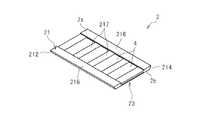
図2A及び図2Bは、雄型コネクタ2の斜視図及び分解斜視図である。雄型コネクタ2は、梯子状に形成された樹脂製の第1のフレーム21と、複数の端子25が設けられた端子保持体23と、各端子25上に設けられた誘電体部4とを有している。 2A and 2B are a perspective view and an exploded perspective view of the
第1のフレーム21は、一対の長辺部216と、これらを連結する複数の連結部217とを有しており、連結部217の間には、穴部218が形成されている。端子保持体23は、この第1のフレーム21の裏面2b側に取り付けられる。穴部218の位置は、端子25の位置に対応しており、各穴部218内には、誘電体部4が収容される。また、長辺部216の外縁には、表面2a側が裏面2b側よりも外方に張り出したテーパー部212,214がそれぞれ形成されている。 The
端子保持体23は、樹脂製の板状基材232と、この板状基材232に巻き付けられるように形成される導体膜252とを有しており、この導体膜252により端子25が構成される。具体的な例では、板状基材232としてのBT(ビスマレイミド・トリアジン)樹脂の表面の一部に、ニッケル下地めっき及び金めっきが施され、その上に、導体膜252としての銅箔が配置される。なお、端子保持体23は、端子25としての金属板に樹脂材を一体成形することで得られてもよい。 The
誘電体部4は、例えば五酸化タンタルやチタン酸バリウムなどの高誘電セラミックからなり、端子25の表面25aに接合される。具体的な例では、誘電体部4の表面に銅層が蒸着等で形成され、この銅層が端子25の表面25aに半田等で接合される。これにより、端子25と誘電体部4との間に空気層が形成されることが抑制される。なお、誘電体部4は、スパッタリングや印刷などで端子25上に形成されてもよい。 The
図3は、雄型コネクタ2の実装を表す図である。雄型コネクタ2が実装される第1の平型回路基材7は、複数の電気回路73を有し、各電気回路73の端部には、導体パッド75が形成されている。この導体パッド75は、第1の平型回路基材7に形成された導体パターンが露出した、接続用の導体パターンである。雄型コネクタ2の第1のフレーム21の裏面2bは、第1の平型回路基材7の表面に接着され、端子25(図2Bを参照)の裏面は、第1の平型回路基材7に設けられた導体パッド75に接続される。 FIG. 3 is a diagram illustrating the mounting of the
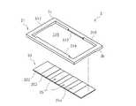
図4A及び図4Bは、雌型コネクタ3の斜視図及び分解斜視図である。雌型コネクタ3は、矩形枠状に形成された、適度な弾性を有する樹脂製の第2のフレーム31と、複数の端子35が設けられた端子保持体33とを有している。 4A and 4B are a perspective view and an exploded perspective view of the
第2のフレーム31は、一対の長辺部316と、一対の短辺部317とを有しており、これらが穴部318を取り囲んでいる。この穴部318内には、上記第1のフレーム21が嵌め入れられる。端子保持体33は、この第2のフレーム31の裏面3b側に取り付けられる。また、長辺部316の内縁には、表面3a側が裏面3b側よりも内方に張り出したテーパー部312,314がそれぞれ形成されている。 The
端子保持体33は、上述の端子保持体23と同様に、樹脂製の板状基材332と、この板状基材332に巻き付けられるように形成される導体膜352とを有しており、この導体膜352により端子35が構成される。 The
図5は、雌型コネクタ3の実装を表す図である。雌型コネクタ3が実装される第2の平型回路基材8は、上述の第1の平型回路基材7と同様に、複数の電気回路83を有し、各電気回路83の端部には、導体パッド85が形成されている。この導体パッド85は、第2の平型回路基材8に形成された導体パターンが露出した、接続用の導体パターンである。雌型コネクタ3の第2のフレーム31の裏面3bは、第2の平型回路基材8の表面に接着され、端子35の裏面は、第2の平型回路基材8に設けられた導体パッド85に接続される。 FIG. 5 is a diagram illustrating the mounting of the
なお、第2のフレーム31の長辺部316の弾性変形を可能とするため、第2のフレーム31の裏面3bのうち、短辺部317の裏面のみが第2の平型回路基材8の表面に接着され、長辺部316の裏面は第2の平型回路基材8の表面に接着されないことが好ましい。 In order to enable elastic deformation of the
以上に説明した雄型コネクタ2の第1のフレーム21と、雌型コネクタ3の第2のフレーム31とは、上記図1に示されるように嵌め合わされる。このとき、雄型コネクタ2の端子25上の誘電体部4が、雌型コネクタ3の端子35と接触し、これにより、対向する端子25と端子35との間に誘電体部4が挟み込まれる。 The
具体的には、第1のフレーム21と第2のフレーム31とは、テーパー部212,214とテーパー部312,314とが嵌め合わされることで、互いに引き付け合う力を生じ、これにより、誘電体部4と端子35とが圧接される。なお、こうした態様に限られず、段差形状同士が嵌め合わされる態様であってもよい。 Specifically, the
また、雄型コネクタ2の誘電体部4と雌型コネクタ3の端子35との少なくとも一方には、液状の誘電性材料が塗布されている。このため、第1のフレーム21と第2のフレーム31とが嵌め合わされるとき、図6に示されるように、誘電体部4と端子35(詳しくは導体膜352)との間に形成される微小な隙間に、液状の誘電性材料45が介在する。この液状の誘電性材料45は、室温近傍で液状であり、空気よりも誘電率が高い材料である。 Further, at least one of the
詳しくは、液状の誘電性材料45の主成分としては、誘電率が比較的高いグリコール系の樹脂が好適に用いられる。さらに、グリコール系の樹脂としては、例えばPPG(ポリプロピレングリコール トリオール型 M=1500)等が好適に用いられる。このPPGは、25℃で200〜500mPa・s程度の粘性を有しており、誘電体部4又は端子35上から流れ落ちにくい。 Specifically, as the main component of the liquid
これに限られず、液状の誘電性材料45の主成分は、例えばシリコーンオイル、ワセリン又はアクリル樹脂などであってもよい。特にシリコーンオイルは、優れた耐熱性を有するため、高温を伴う製造の観点から好適である。 However, the main component of the liquid
以上に説明した本発明の実施形態によれば、誘電体部4と端子35との間の微小な隙間に液状の誘電性材料45が介在するので、端子25と端子35との間の静電容量の劣化が抑制される。また、液状の誘電性材料45が用いられることで、誘電体部4と端子35との接触が可能であると共に、誘電体部4と端子35との間の微小な隙間の充填が可能である。また、液状の誘電性材料45が用いられることで、図4Aに示されるように、複数の端子35が平面的に配列する場合であっても、端子35間の短絡が抑制される。 According to the embodiment of the present invention described above, since the liquid
また、端子25及び端子35が配置されることで、第1の平型回路基材7と第2の平型回路基材8との間にスペースが確保されるので、これらを連結するための第1のフレーム21及び第2のフレーム31を配置することが可能である。 In addition, since the terminal 25 and the terminal 35 are arranged, a space is secured between the first flat
なお、こうした態様に限られず、例えば、図7に示されるように、上記図1の構成から端子35が省略され、雄型コネクタ2の端子25上の誘電体部4が、第2の平型回路基材8の導体パッド85(図5を参照)に接触し、これらの隙間に液状の誘電性材料が介在してもよい。 For example, as shown in FIG. 7, the terminal 35 is omitted from the configuration shown in FIG. 1, and the
また、例えば、上記図1の構成において端子35上にも誘電体部が設けられ、雄型コネクタ2の端子25上の誘電体部4が、雌型コネクタ3の端子35上の誘電体部と接触し、これらの隙間に液状の誘電性材料が介在してもよい。 Further, for example, in the configuration of FIG. 1, a dielectric part is also provided on the terminal 35, and the
以下、本発明の電気回路の接続構造および電気回路の接続方法の他の実施形態について説明する。図8及び図9は、他の実施形態を表す分解斜視図および断面図である。上記実施形態と重複する構成については、同番号を付すことで詳細な説明を省略する。 Hereinafter, other embodiments of the electrical circuit connection structure and electrical circuit connection method of the present invention will be described. 8 and 9 are an exploded perspective view and a cross-sectional view showing another embodiment. About the structure which overlaps with the said embodiment, detailed description is abbreviate | omitted by attaching | subjecting the same number.
本実施形態では、第1の平型回路基材7に形成された導体パッド75が導体部とされ、この導体パッド75上に誘電体部4が配置される。また、第2の平型回路基材8に形成された導体パッド85は対向部とされる。 In the present embodiment, the
第1の平型回路基材7及び第2の平型回路基材8は、誘電体部4と導体パッド85とが接触するように重ね合わせられ、略C字形状の留め具6によって挟まれて固定される。このとき、導体パッド75と導体パッド85とが誘電体部4を挟んで対向し、容量結合が実現する。 The first
留め具6は、第1の平型回路基材7の裏面に当接する支持部67と、第2の平型回路基材8の裏面に当接し、弾性変形により第2の平型回路基材8を第1の平型回路基材7の側へ押圧する弾性変形部68と、これら支持部67と弾性変形部68とを連結する連結部69と、を備える。 The
誘電体部4と導体パッド85との少なくとも一方には、液状の誘電性材料が塗布されている。このため、誘電体部4と導体パッド85との間に形成される微小な隙間には、上記図6と同様に液状の誘電性材料が介在し、その結果、導体パッド75と導体パッド85との間の静電容量の劣化が抑制される。 A liquid dielectric material is applied to at least one of the
また、液状の誘電性材料が用いられることで、誘電体部4と導体パッド85との接触が可能であると共に、誘電体部4と導体パッド85との間の微小な隙間の充填が可能である。また、液状の誘電性材料が用いられることで、複数の導体パッド85が平面的に配列する場合であっても、導体パッド85間の短絡が抑制される。 Further, by using a liquid dielectric material, the
また、上述のような端子25,35を介さずに、導体パッド75と導体パッド85とが誘電体部4を挟み込むことで、第1の平型回路基材7と第2の平型回路基材8との距離が短縮化される。 Further, the
以上、本発明の実施形態について説明したが、本発明は上記実施形態に限定されるものではなく、種々の変形実施が当業者にとって可能であるのはもちろんである。 Although the embodiments of the present invention have been described above, the present invention is not limited to the above-described embodiments, and various modifications can be made by those skilled in the art.
1 コネクタ、2 雄型コネクタ、21 第1のフレーム、212,214 テーパー部、216 長辺部、217 連結部、218 穴部、23 端子保持体、232 板状基材、25 端子(導体部)、252 導体膜、3 雌型コネクタ、31 第2のフレーム、312,314 テーパー部、316 長辺部、317 短辺部、318 穴部、33 端子保持体、332 板状基材、35 端子(対向部)、352 導体膜、4 誘電体部、45 液状の誘電体材料、6 留め具、67 支持部、68 弾性変形部、69 連結部、7 第1の平型回路基材、73 電気回路、75 導体パッド、8 第2の平型回路基材、83 電気回路、85 導体パッド。 DESCRIPTION OF
Claims (12)
Translated fromJapanese前記各導体部上に設けられる誘電体部と、
第2の平型回路基材の側に設けられる1又は複数の対向部と、
を備え、
前記誘電体部が前記対向部に対向すると共に、前記誘電体部と前記対向部との隙間に液状の誘電性材料が介在する、
ことを特徴とする電気回路の接続構造。One or more conductor portions that are electrically connected to the electric circuit of the first flat circuit substrate;
A dielectric portion provided on each conductor portion;
One or more opposing portions provided on the second flat circuit substrate side;
With
The dielectric portion is opposed to the facing portion, and a liquid dielectric material is interposed in a gap between the dielectric portion and the facing portion.
An electrical circuit connection structure characterized by that.
請求項1に記載の電気回路の接続構造。The dielectric portion is in contact with the facing portion, and a liquid dielectric material is interposed in the gap between the dielectric portion and the facing portion.
The electrical circuit connection structure according to claim 1.
請求項1に記載の電気回路の接続構造。The conductor portion is a conductor pad formed on the first flat circuit substrate;
The electrical circuit connection structure according to claim 1.
請求項1に記載の電気回路の接続構造。The facing portion is a conductor pad formed on the second flat circuit substrate.
The electrical circuit connection structure according to claim 1.
前記対向部が前記第2の平型回路基材に形成された導体パッドである、
請求項1に記載の電気回路の接続構造。The conductor portion is a conductor pad formed on the first flat circuit substrate;
The facing portion is a conductor pad formed on the second flat circuit substrate.
The electrical circuit connection structure according to claim 1.
請求項1に記載の電気回路の接続構造。The conductor portion is formed in a plate shape, the electric circuit is connected to one surface, and the dielectric portion is provided on the other surface.
The electrical circuit connection structure according to claim 1.
請求項1に記載の電気回路の接続構造。The opposing portion is formed in a plate shape, the electric circuit is connected to one surface, and the dielectric portion is in contact with the other surface through the liquid dielectric material,
The electrical circuit connection structure according to claim 1.
前記導体部の一方の面に前記電気回路が接続され、他方の面上に前記誘電体部が設けられ、
前記対向部の一方の面に前記電気回路が接続され、他方の面に前記液状の誘電性材料を介して前記誘電体部が接触する、
請求項1に記載の電気回路の接続構造。The conductor portion and the facing portion are formed in a plate shape,
The electric circuit is connected to one surface of the conductor portion, and the dielectric portion is provided on the other surface,
The electric circuit is connected to one surface of the facing portion, and the dielectric portion is in contact with the other surface via the liquid dielectric material,
The electrical circuit connection structure according to claim 1.
請求項1ないし8の何れかに記載の電気回路の接続構造。The main component of the liquid dielectric material is a glycol-based resin,
The electrical circuit connection structure according to claim 1.
ことを特徴とする電気回路の接続方法。A dielectric portion provided on one or more conductor portions that are electrically connected to an electric circuit of the first flat circuit substrate, one or more opposing portions provided on the second flat circuit substrate side, And a liquid dielectric material is interposed in the gap between the dielectric portion and the facing portion.
A method for connecting an electric circuit.
請求項10に記載の電気回路の接続方法。The dielectric portion is in contact with the facing portion, and a liquid dielectric material is interposed in the gap between the dielectric portion and the facing portion.
The electrical circuit connection method according to claim 10.
請求項10または11に記載の電気回路の接続方法。
The main component of the liquid dielectric material is a glycol-based resin,
The connection method of the electric circuit of Claim 10 or 11.
Priority Applications (5)
| Application Number | Priority Date | Filing Date | Title |
|---|---|---|---|
| JP2009019765AJP5113101B2 (en) | 2009-01-30 | 2009-01-30 | Electrical circuit connection structure and electrical circuit connection method |
| CN201080016005.3ACN102379167B (en) | 2009-01-30 | 2010-02-01 | Use the adapter of liquid dielectric for improved performance |
| PCT/US2010/022694WO2010088582A2 (en) | 2009-01-30 | 2010-02-01 | Connector using liquid dielectric for improved performance |
| US13/146,477US9004925B2 (en) | 2009-01-30 | 2010-02-01 | Capacitively coupled connector using liquid dielectric for improved performance |
| KR1020117020026AKR20110110852A (en) | 2009-01-30 | 2010-02-01 | Connectors with liquid dielectrics for improved performance |
Applications Claiming Priority (1)
| Application Number | Priority Date | Filing Date | Title |
|---|---|---|---|
| JP2009019765AJP5113101B2 (en) | 2009-01-30 | 2009-01-30 | Electrical circuit connection structure and electrical circuit connection method |
Publications (2)
| Publication Number | Publication Date |
|---|---|
| JP2010177102A JP2010177102A (en) | 2010-08-12 |
| JP5113101B2true JP5113101B2 (en) | 2013-01-09 |
Family
ID=42396382
Family Applications (1)
| Application Number | Title | Priority Date | Filing Date |
|---|---|---|---|
| JP2009019765AExpired - Fee RelatedJP5113101B2 (en) | 2009-01-30 | 2009-01-30 | Electrical circuit connection structure and electrical circuit connection method |
Country Status (5)
| Country | Link |
|---|---|
| US (1) | US9004925B2 (en) |
| JP (1) | JP5113101B2 (en) |
| KR (1) | KR20110110852A (en) |
| CN (1) | CN102379167B (en) |
| WO (1) | WO2010088582A2 (en) |
Families Citing this family (2)
| Publication number | Priority date | Publication date | Assignee | Title |
|---|---|---|---|---|
| GB2501570B (en)* | 2012-12-18 | 2014-04-16 | Novalia Ltd | Capacitive touch device |
| US9455529B2 (en)* | 2014-05-23 | 2016-09-27 | Intel Corporation | Proximity capacitive coupling for board-to-board wide bandwidth transmissions |
Family Cites Families (71)
| Publication number | Priority date | Publication date | Assignee | Title |
|---|---|---|---|---|
| GB1250379A (en)* | 1969-08-25 | 1971-10-20 | ||
| US3611225A (en) | 1970-06-24 | 1971-10-05 | Westinghouse Electric Corp | Electrical inductive apparatus having liquid and solid dielectric means |
| US4144485A (en) | 1974-12-03 | 1979-03-13 | Nippon Soken, Inc. | Contactless connector circuit |
| US4117579A (en)* | 1976-06-01 | 1978-10-03 | General Electric Company | Method of impregnating a capacitor |
| GB8501155D0 (en) | 1985-01-17 | 1985-02-20 | Shell Int Research | Capacitive underwater electrical connector |
| US4647126A (en) | 1985-06-17 | 1987-03-03 | Sperry Corporation | Compliant lead clip |
| US4770641A (en)* | 1986-03-31 | 1988-09-13 | Amp Incorporated | Conductive gel interconnection apparatus |
| US4716058A (en) | 1986-08-25 | 1987-12-29 | Sprague Electric Company | Method of curtain coating to make thin dielectric ceramic layers |
| US5037312A (en) | 1990-11-15 | 1991-08-06 | Amp Incorporated | Conductive gel area array connector |
| US5298288A (en) | 1991-02-14 | 1994-03-29 | Microelectronics And Computer Technology Corporation | Coating a heat curable liquid dielectric on a substrate |
| US5074799A (en) | 1991-03-27 | 1991-12-24 | Amp Incorporated | Gel connector of laminar construction |
| US5432486A (en) | 1993-05-20 | 1995-07-11 | Northern Telecom Limited | Capacitive and inductive coupling connector |
| FR2706649B1 (en) | 1993-06-14 | 1998-05-07 | Hitachi Maxell | Data transfer system comprising an electromagnetic coupling connector and electromagnetic coupling connector of this system. |
| US5403202A (en) | 1993-10-07 | 1995-04-04 | Hewlett-Packard Company | Low insertion force/low profile flex connector |
| US5791943A (en) | 1995-11-22 | 1998-08-11 | The Siemon Company | Reduced crosstalk modular outlet |
| US5769647A (en) | 1995-11-22 | 1998-06-23 | The Siemon Company | Modular outlet employing a door assembly |
| EP0872022B1 (en) | 1996-01-02 | 2000-03-29 | International Business Machines Corporation | Pcmcia rf connector |
| US5921787A (en) | 1996-07-17 | 1999-07-13 | Minnesota Mining And Manufacturing Company | Board-to-board interconnection |
| JPH1174043A (en) | 1997-08-29 | 1999-03-16 | Molex Inc | Locking structure for connection of flat flexible cable connector with cable |
| US6007359A (en) | 1997-11-25 | 1999-12-28 | Itt Manufacturing Enterprises, Inc. | Receptacle connector |
| JP2000260506A (en) | 1999-03-10 | 2000-09-22 | Fujitsu Takamisawa Component Ltd | Connector and manufacture thereof |
| US6358064B2 (en) | 1999-03-29 | 2002-03-19 | Delphi Technologies, Inc. | Z-axis electrical interconnect |
| US6498305B1 (en) | 1999-05-25 | 2002-12-24 | Intel Corporation | Interconnect mechanics for electromagnetic coupler |
| US6452113B2 (en) | 1999-07-15 | 2002-09-17 | Incep Technologies, Inc. | Apparatus for providing power to a microprocessor with integrated thermal and EMI management |
| US6957963B2 (en) | 2000-01-20 | 2005-10-25 | Gryphics, Inc. | Compliant interconnect assembly |
| US6939143B2 (en)* | 2000-01-20 | 2005-09-06 | Gryphics, Inc. | Flexible compliant interconnect assembly |
| US6317011B1 (en) | 2000-03-09 | 2001-11-13 | Avaya Technology Corp. | Resonant capacitive coupler |
| US6612852B1 (en) | 2000-04-13 | 2003-09-02 | Molex Incorporated | Contactless interconnection system |
| JP3465671B2 (en) | 2000-08-09 | 2003-11-10 | 株式会社村田製作所 | Converter device |
| JP3929763B2 (en) | 2001-01-12 | 2007-06-13 | 株式会社オートネットワーク技術研究所 | Connector for flat wiring material |
| JP2002289309A (en)* | 2001-03-28 | 2002-10-04 | Jst Mfg Co Ltd | Electrical connector |
| US6885090B2 (en) | 2001-11-28 | 2005-04-26 | North Carolina State University | Inductively coupled electrical connectors |
| US6657866B2 (en) | 2002-03-15 | 2003-12-02 | Robert C. Morelock | Electronics assembly with improved heatsink configuration |
| US7265565B2 (en) | 2003-02-04 | 2007-09-04 | Microfabrica Inc. | Cantilever microprobes for contacting electronic components and methods for making such probes |
| WO2004010538A1 (en) | 2002-07-23 | 2004-01-29 | Matsushita Electric Works, Ltd. | Low-profile connector |
| US6903941B2 (en) | 2002-10-24 | 2005-06-07 | Hewlett-Packard Development Company, L.P. | Printed circuit board assembly employing a press fit electrical connector |
| JP4330913B2 (en) | 2003-04-03 | 2009-09-16 | 三陽機器株式会社 | Front loader with work vehicle stand |
| US6806542B1 (en)* | 2003-06-30 | 2004-10-19 | Motorola, Inc. | Electronic device having a filled dielectric medium |
| GB2404094B (en) | 2003-07-17 | 2008-01-02 | Thales Plc | Electrical connector |
| JP3956920B2 (en) | 2003-08-26 | 2007-08-08 | 松下電工株式会社 | connector |
| US6951466B2 (en) | 2003-09-02 | 2005-10-04 | Hewlett-Packard Development Company, L.P. | Attachment plate for directly mating circuit boards |
| US6811411B1 (en) | 2003-09-12 | 2004-11-02 | Molex Incorporated | Board-to-board electrical connector assembly |
| US7147514B2 (en) | 2004-02-05 | 2006-12-12 | Hewlett-Packard Development Company, L.P. | Connector providing capacitive coupling |
| JP5008823B2 (en) | 2004-03-19 | 2012-08-22 | シャープ株式会社 | Display device |
| JP2006120511A (en) | 2004-10-22 | 2006-05-11 | Nec Corp | Connector for connection inter-circuit boards |
| JP2006174262A (en)* | 2004-12-17 | 2006-06-29 | Mitsubishi Electric Corp | Board connection structure |
| US7671449B2 (en) | 2005-05-04 | 2010-03-02 | Sun Microsystems, Inc. | Structures and methods for an application of a flexible bridge |
| JP4632870B2 (en)* | 2005-06-10 | 2011-02-16 | Necシステムテクノロジー株式会社 | LSI package and circuit board |
| JP2007035291A (en) | 2005-07-22 | 2007-02-08 | Hirose Electric Co Ltd | Electrical connector |
| JP2007105155A (en) | 2005-10-12 | 2007-04-26 | Matsushita Electric Ind Co Ltd | Hand dryer |
| TW200719787A (en) | 2005-11-11 | 2007-05-16 | Innolux Display Corp | Circuit board and electronic device using the same |
| CN100502618C (en) | 2006-01-05 | 2009-06-17 | 友达光电股份有限公司 | Circuit board module and method of forming same |
| TW200737604A (en) | 2006-03-29 | 2007-10-01 | Altek Corp | Electrical connector structure |
| JP4303259B2 (en) | 2006-05-15 | 2009-07-29 | 京セラエルコ株式会社 | Connector and portable terminal equipped with this connector |
| KR101231305B1 (en) | 2006-05-25 | 2013-02-07 | 엘지이노텍 주식회사 | camera module assembly |
| JP2007328961A (en) | 2006-06-06 | 2007-12-20 | Kyocera Elco Corp | Connector device |
| JP4843423B2 (en) | 2006-09-05 | 2011-12-21 | アイティーティー マニュファクチャリング エンタープライジーズ, インコーポレイテッド | Connector and contacts used for the connector |
| CN201029125Y (en) | 2007-03-02 | 2008-02-27 | 富士康(昆山)电脑接插件有限公司 | Cable Connector Assembly |
| JP2008262828A (en) | 2007-04-12 | 2008-10-30 | Alps Electric Co Ltd | Planar connector |
| US7537458B2 (en) | 2007-04-25 | 2009-05-26 | Research In Motion Limited | Connector for electronic devices |
| CN101295848B (en) | 2007-04-27 | 2010-06-09 | 鸿富锦精密工业(深圳)有限公司 | Electric connector and camera device with the same |
| US7530839B1 (en) | 2008-04-15 | 2009-05-12 | Jess-Link Products Co., Ltd. | Electrical connector |
| JP4932789B2 (en)* | 2008-04-28 | 2012-05-16 | モレックス インコーポレイテド | Connector and terminal holder |
| JP2009301740A (en)* | 2008-06-10 | 2009-12-24 | Molex Inc | Connector and terminal support |
| US8157598B2 (en)* | 2008-06-10 | 2012-04-17 | Molex Incorporated | Input/output connector with capacitive coupling mating interface |
| WO2009151803A1 (en) | 2008-06-10 | 2009-12-17 | Molex Incorporated | Capacitively coupled connector for flexible printed circuit applications |
| US8287289B2 (en)* | 2008-06-10 | 2012-10-16 | Molex Incorporated | Elastic-cushioned capacitively-coupled connector |
| JP2010086827A (en) | 2008-09-30 | 2010-04-15 | Molex Inc | Electrical connector |
| JP2010177103A (en)* | 2009-01-30 | 2010-08-12 | Molex Inc | Connector and terminal holder |
| US8197286B2 (en) | 2009-06-11 | 2012-06-12 | Commscope, Inc. Of North Carolina | Communications plugs having capacitors that inject offending crosstalk after a plug-jack mating point and related connectors and methods |
| JP5462732B2 (en)* | 2010-06-29 | 2014-04-02 | モレックス インコーポレイテド | Sheet-like connector and manufacturing method thereof |
- 2009
- 2009-01-30JPJP2009019765Apatent/JP5113101B2/ennot_activeExpired - Fee Related
- 2010
- 2010-02-01WOPCT/US2010/022694patent/WO2010088582A2/enactiveApplication Filing
- 2010-02-01CNCN201080016005.3Apatent/CN102379167B/ennot_activeExpired - Fee Related
- 2010-02-01USUS13/146,477patent/US9004925B2/ennot_activeExpired - Fee Related
- 2010-02-01KRKR1020117020026Apatent/KR20110110852A/ennot_activeAbandoned
Also Published As
| Publication number | Publication date |
|---|---|
| US9004925B2 (en) | 2015-04-14 |
| CN102379167B (en) | 2016-11-16 |
| WO2010088582A3 (en) | 2011-01-06 |
| WO2010088582A2 (en) | 2010-08-05 |
| KR20110110852A (en) | 2011-10-07 |
| JP2010177102A (en) | 2010-08-12 |
| CN102379167A (en) | 2012-03-14 |
| US20110279946A1 (en) | 2011-11-17 |
Similar Documents
| Publication | Publication Date | Title |
|---|---|---|
| US10943740B2 (en) | Electrical connection contact for a ceramic component, a ceramic component, and a component arrangement | |
| CN105826353B (en) | Flip chip and display device | |
| CN204991657U (en) | Electronic component and circuit board | |
| JP4863130B2 (en) | Board connector, semiconductor device socket including the same, cable connector, and board-to-board connector | |
| US8287289B2 (en) | Elastic-cushioned capacitively-coupled connector | |
| JP2015095490A (en) | Ceramic electronic component | |
| EP3293952B1 (en) | Fingerprint module, method for fabricating the same, and mobile terminal having the same | |
| JP2010193059A5 (en) | ||
| CN113692110A (en) | Flexible circuit board and mobile terminal | |
| JP2007329431A (en) | Piezoelectric exciter | |
| US20180054896A1 (en) | Fingerprint Module, Method For Manufacturing The Fingerprint Module, And Mobile Terminal | |
| CN215268953U (en) | Resin multilayer substrate | |
| JP5113101B2 (en) | Electrical circuit connection structure and electrical circuit connection method | |
| KR200442294Y1 (en) | Solderable Elastic Electrical Contact Terminals | |
| CN205902188U (en) | Electrical components and mobile devices | |
| CN105379005A (en) | structure | |
| JP2012226902A (en) | Connection structure for chip component to conductive member | |
| WO2019098391A1 (en) | Movable contact body for switch, and switch | |
| JP2010177103A (en) | Connector and terminal holder | |
| CN113036571B (en) | Preparation method of connector, connector and integrated device | |
| US20230420157A1 (en) | Electric contact terminal | |
| CN210112381U (en) | Flexible circuit board | |
| KR102465243B1 (en) | Method for manufacturing circuit board and circuit board manufactured by the method | |
| CN120659213A (en) | Module substrates and electronic devices | |
| US9912315B2 (en) | Composite electronic component and board having the same |
Legal Events
| Date | Code | Title | Description |
|---|---|---|---|
| A621 | Written request for application examination | Free format text:JAPANESE INTERMEDIATE CODE: A621 Effective date:20110908 | |
| TRDD | Decision of grant or rejection written | ||
| A01 | Written decision to grant a patent or to grant a registration (utility model) | Free format text:JAPANESE INTERMEDIATE CODE: A01 Effective date:20121002 | |
| A01 | Written decision to grant a patent or to grant a registration (utility model) | Free format text:JAPANESE INTERMEDIATE CODE: A01 | |
| A61 | First payment of annual fees (during grant procedure) | Free format text:JAPANESE INTERMEDIATE CODE: A61 Effective date:20121011 | |
| FPAY | Renewal fee payment (event date is renewal date of database) | Free format text:PAYMENT UNTIL: 20151019 Year of fee payment:3 | |
| R150 | Certificate of patent or registration of utility model | Free format text:JAPANESE INTERMEDIATE CODE: R150 | |
| S533 | Written request for registration of change of name | Free format text:JAPANESE INTERMEDIATE CODE: R313533 | |
| LAPS | Cancellation because of no payment of annual fees | ||
| R350 | Written notification of registration of transfer | Free format text:JAPANESE INTERMEDIATE CODE: R350 |