JP5110927B2 - Electro-optical device and electronic apparatus - Google Patents
Electro-optical device and electronic apparatusDownload PDFInfo
- Publication number
- JP5110927B2 JP5110927B2JP2007078304AJP2007078304AJP5110927B2JP 5110927 B2JP5110927 B2JP 5110927B2JP 2007078304 AJP2007078304 AJP 2007078304AJP 2007078304 AJP2007078304 AJP 2007078304AJP 5110927 B2JP5110927 B2JP 5110927B2
- Authority
- JP
- Japan
- Prior art keywords
- electrode
- electro
- region
- liquid crystal
- pixel
- Prior art date
- Legal status (The legal status is an assumption and is not a legal conclusion. Google has not performed a legal analysis and makes no representation as to the accuracy of the status listed.)
- Expired - Fee Related
Links
- 239000000758substrateSubstances0.000claimsdescription82
- 230000005684electric fieldEffects0.000claimsdescription54
- 239000000463materialSubstances0.000claimsdescription33
- 230000003287optical effectEffects0.000claimsdescription21
- 239000000382optic materialSubstances0.000claimsdescription16
- 239000004990Smectic liquid crystalSubstances0.000claimsdescription9
- 230000003098cholesteric effectEffects0.000claimsdescription5
- 239000000693micelleSubstances0.000claimsdescription3
- 239000010410layerSubstances0.000description155
- 239000004973liquid crystal related substanceSubstances0.000description151
- 238000002834transmittanceMethods0.000description38
- 239000011347resinSubstances0.000description19
- 229920005989resinPolymers0.000description19
- 239000010409thin filmSubstances0.000description18
- 230000005540biological transmissionEffects0.000description15
- 239000004065semiconductorSubstances0.000description14
- 238000000034methodMethods0.000description11
- 230000005374Kerr effectEffects0.000description9
- 230000008569processEffects0.000description8
- 239000010408filmSubstances0.000description7
- 239000011159matrix materialSubstances0.000description7
- 239000011295pitchSubstances0.000description7
- 230000004044responseEffects0.000description6
- 230000008859changeEffects0.000description5
- 239000003566sealing materialSubstances0.000description5
- VYZAMTAEIAYCRO-UHFFFAOYSA-NChromiumChemical compound[Cr]VYZAMTAEIAYCRO-UHFFFAOYSA-N0.000description4
- 229910052782aluminiumInorganic materials0.000description4
- XAGFODPZIPBFFR-UHFFFAOYSA-NaluminiumChemical compound[Al]XAGFODPZIPBFFR-UHFFFAOYSA-N0.000description4
- 229910052804chromiumInorganic materials0.000description4
- 239000011651chromiumSubstances0.000description4
- 230000001747exhibiting effectEffects0.000description4
- 229910052751metalInorganic materials0.000description4
- 239000002184metalSubstances0.000description4
- 230000002093peripheral effectEffects0.000description4
- 230000001105regulatory effectEffects0.000description4
- 125000006850spacer groupChemical group0.000description4
- 239000004020conductorSubstances0.000description3
- 229910052715tantalumInorganic materials0.000description3
- GUVRBAGPIYLISA-UHFFFAOYSA-Ntantalum atomChemical compound[Ta]GUVRBAGPIYLISA-UHFFFAOYSA-N0.000description3
- 239000004988Nematic liquid crystalSubstances0.000description2
- 229910004298SiO 2Inorganic materials0.000description2
- 238000010586diagramMethods0.000description2
- 238000009792diffusion processMethods0.000description2
- 239000011521glassSubstances0.000description2
- 238000002347injectionMethods0.000description2
- 239000007924injectionSubstances0.000description2
- 229910010272inorganic materialInorganic materials0.000description2
- 239000011147inorganic materialSubstances0.000description2
- LQNUZADURLCDLV-UHFFFAOYSA-NnitrobenzeneChemical compound[O-][N+](=O)C1=CC=CC=C1LQNUZADURLCDLV-UHFFFAOYSA-N0.000description2
- 239000011368organic materialSubstances0.000description2
- 239000004033plasticSubstances0.000description2
- 230000010287polarizationEffects0.000description2
- 229920000642polymerPolymers0.000description2
- 239000010453quartzSubstances0.000description2
- VYPSYNLAJGMNEJ-UHFFFAOYSA-Nsilicon dioxideInorganic materialsO=[Si]=OVYPSYNLAJGMNEJ-UHFFFAOYSA-N0.000description2
- 239000004925Acrylic resinSubstances0.000description1
- 229920000178Acrylic resinPolymers0.000description1
- 241000205407PolygonumSpecies0.000description1
- 229910021417amorphous siliconInorganic materials0.000description1
- 230000001413cellular effectEffects0.000description1
- 230000008034disappearanceEffects0.000description1
- 230000000694effectsEffects0.000description1
- 239000012777electrically insulating materialSubstances0.000description1
- 230000006872improvementEffects0.000description1
- AMGQUBHHOARCQH-UHFFFAOYSA-Nindium;oxotinChemical compound[In].[Sn]=OAMGQUBHHOARCQH-UHFFFAOYSA-N0.000description1
- 239000011810insulating materialSubstances0.000description1
- 239000011229interlayerSubstances0.000description1
- 230000004048modificationEffects0.000description1
- 238000012986modificationMethods0.000description1
- 229910052709silverInorganic materials0.000description1
- 239000004332silverSubstances0.000description1
- 239000000126substanceSubstances0.000description1
- 239000012780transparent materialSubstances0.000description1
Images


Classifications
- G—PHYSICS
- G02—OPTICS
- G02F—OPTICAL DEVICES OR ARRANGEMENTS FOR THE CONTROL OF LIGHT BY MODIFICATION OF THE OPTICAL PROPERTIES OF THE MEDIA OF THE ELEMENTS INVOLVED THEREIN; NON-LINEAR OPTICS; FREQUENCY-CHANGING OF LIGHT; OPTICAL LOGIC ELEMENTS; OPTICAL ANALOGUE/DIGITAL CONVERTERS
- G02F1/00—Devices or arrangements for the control of the intensity, colour, phase, polarisation or direction of light arriving from an independent light source, e.g. switching, gating or modulating; Non-linear optics
- G02F1/01—Devices or arrangements for the control of the intensity, colour, phase, polarisation or direction of light arriving from an independent light source, e.g. switching, gating or modulating; Non-linear optics for the control of the intensity, phase, polarisation or colour
- G02F1/13—Devices or arrangements for the control of the intensity, colour, phase, polarisation or direction of light arriving from an independent light source, e.g. switching, gating or modulating; Non-linear optics for the control of the intensity, phase, polarisation or colour based on liquid crystals, e.g. single liquid crystal display cells
- G02F1/133—Constructional arrangements; Operation of liquid crystal cells; Circuit arrangements
- G02F1/1333—Constructional arrangements; Manufacturing methods
- G02F1/1335—Structural association of cells with optical devices, e.g. polarisers or reflectors
- G02F1/133528—Polarisers
- G02F1/133543—Cholesteric polarisers
- G—PHYSICS
- G02—OPTICS
- G02F—OPTICAL DEVICES OR ARRANGEMENTS FOR THE CONTROL OF LIGHT BY MODIFICATION OF THE OPTICAL PROPERTIES OF THE MEDIA OF THE ELEMENTS INVOLVED THEREIN; NON-LINEAR OPTICS; FREQUENCY-CHANGING OF LIGHT; OPTICAL LOGIC ELEMENTS; OPTICAL ANALOGUE/DIGITAL CONVERTERS
- G02F1/00—Devices or arrangements for the control of the intensity, colour, phase, polarisation or direction of light arriving from an independent light source, e.g. switching, gating or modulating; Non-linear optics
- G02F1/01—Devices or arrangements for the control of the intensity, colour, phase, polarisation or direction of light arriving from an independent light source, e.g. switching, gating or modulating; Non-linear optics for the control of the intensity, phase, polarisation or colour
- G02F1/13—Devices or arrangements for the control of the intensity, colour, phase, polarisation or direction of light arriving from an independent light source, e.g. switching, gating or modulating; Non-linear optics for the control of the intensity, phase, polarisation or colour based on liquid crystals, e.g. single liquid crystal display cells
- G02F1/137—Devices or arrangements for the control of the intensity, colour, phase, polarisation or direction of light arriving from an independent light source, e.g. switching, gating or modulating; Non-linear optics for the control of the intensity, phase, polarisation or colour based on liquid crystals, e.g. single liquid crystal display cells characterised by the electro-optical or magneto-optical effect, e.g. field-induced phase transition, orientation effect, guest-host interaction or dynamic scattering
- G02F1/13718—Devices or arrangements for the control of the intensity, colour, phase, polarisation or direction of light arriving from an independent light source, e.g. switching, gating or modulating; Non-linear optics for the control of the intensity, phase, polarisation or colour based on liquid crystals, e.g. single liquid crystal display cells characterised by the electro-optical or magneto-optical effect, e.g. field-induced phase transition, orientation effect, guest-host interaction or dynamic scattering based on a change of the texture state of a cholesteric liquid crystal
- G—PHYSICS
- G02—OPTICS
- G02F—OPTICAL DEVICES OR ARRANGEMENTS FOR THE CONTROL OF LIGHT BY MODIFICATION OF THE OPTICAL PROPERTIES OF THE MEDIA OF THE ELEMENTS INVOLVED THEREIN; NON-LINEAR OPTICS; FREQUENCY-CHANGING OF LIGHT; OPTICAL LOGIC ELEMENTS; OPTICAL ANALOGUE/DIGITAL CONVERTERS
- G02F1/00—Devices or arrangements for the control of the intensity, colour, phase, polarisation or direction of light arriving from an independent light source, e.g. switching, gating or modulating; Non-linear optics
- G02F1/01—Devices or arrangements for the control of the intensity, colour, phase, polarisation or direction of light arriving from an independent light source, e.g. switching, gating or modulating; Non-linear optics for the control of the intensity, phase, polarisation or colour
- G02F1/13—Devices or arrangements for the control of the intensity, colour, phase, polarisation or direction of light arriving from an independent light source, e.g. switching, gating or modulating; Non-linear optics for the control of the intensity, phase, polarisation or colour based on liquid crystals, e.g. single liquid crystal display cells
- G02F1/137—Devices or arrangements for the control of the intensity, colour, phase, polarisation or direction of light arriving from an independent light source, e.g. switching, gating or modulating; Non-linear optics for the control of the intensity, phase, polarisation or colour based on liquid crystals, e.g. single liquid crystal display cells characterised by the electro-optical or magneto-optical effect, e.g. field-induced phase transition, orientation effect, guest-host interaction or dynamic scattering
- G02F1/13731—Devices or arrangements for the control of the intensity, colour, phase, polarisation or direction of light arriving from an independent light source, e.g. switching, gating or modulating; Non-linear optics for the control of the intensity, phase, polarisation or colour based on liquid crystals, e.g. single liquid crystal display cells characterised by the electro-optical or magneto-optical effect, e.g. field-induced phase transition, orientation effect, guest-host interaction or dynamic scattering based on a field-induced phase transition
Landscapes
- Liquid Crystal (AREA)
Description
Translated fromJapanese本発明は、電気光学装置及び電子機器に関する。 The present invention relates to an electro-optical device and an electronic apparatus.
Kerr効果による電子分極を利用した電気光学装置が知られている。Kerr効果とは、電界を印加したときに当該電界の方向を軸として電界強度の2乗に比例する大きさの光学異方性を示す現象をいう。このようなKerr効果を示す電気光学物質として、例えばブルー相と呼ばれる液晶材料が知られている。液晶層としてブルー相を用いた液晶表示装置は、応答速度が速いことで知られている。ブルー相は、電界が印加されていない状態では光学等方性を呈している。ブルー相が所定範囲内の温度にあるとき、当該ブルー相に電界を印加すると電界強度の2乗に比例する光学異方性を示す。 An electro-optical device using electronic polarization due to the Kerr effect is known. The Kerr effect refers to a phenomenon that exhibits optical anisotropy having a magnitude proportional to the square of the electric field strength with the electric field direction as an axis when an electric field is applied. As an electro-optical substance exhibiting such a Kerr effect, for example, a liquid crystal material called a blue phase is known. A liquid crystal display device using a blue phase as a liquid crystal layer is known for its high response speed. The blue phase exhibits optical isotropy when no electric field is applied. When the blue phase is at a temperature within a predetermined range, an optical anisotropy proportional to the square of the electric field strength is exhibited when an electric field is applied to the blue phase.
近年では、携帯電話機や携帯情報端末等の携帯用電子機器の表示部として、液晶表示装置などの電気光学装置が用いられていることが多い。一般に、携帯用電子機器に用いられる液晶表示装置としては、反射表示及び透過表示が可能な半透過反射型のものが採用されている。特に、横電界方式の液晶表示装置は視野角が広いことで知られている。このような横電界方式の半透過反射型液晶表示装置に液晶層としてブルー相を用いることで、視野角の向上及び高速応答が可能となる(例えば、特許文献1参照。)。 In recent years, electro-optical devices such as liquid crystal display devices are often used as display units of portable electronic devices such as mobile phones and portable information terminals. In general, as a liquid crystal display device used for a portable electronic device, a transflective type capable of reflective display and transmissive display is adopted. In particular, a horizontal electric field type liquid crystal display device is known to have a wide viewing angle. By using a blue phase as a liquid crystal layer in such a transverse electric field type transflective liquid crystal display device, an improvement in viewing angle and a high-speed response are possible (for example, see Patent Document 1).
横電界方式の液晶表示装置は、一般的には、対向配置された一方の基板に液晶層が挟持され、一方の基板上に画素電極と対向電極とが設けられた構成になっている。通常の液晶相は、界面領域の液晶分子の配向が変化することで、周辺の液晶分子にも配向の変化が伝播する特性がある。このため、横電界を印加すると、横電界の印加される領域で液晶分子の配向が変化し、この配向の変化が液晶層の厚さ方向に伝播する。これに対してブルー相は、1個の液晶分子の配向が変化しても、周辺の液晶分子に配向の変化が伝播しにくいという特性がある。このため、ブルー相に横電界を印加した場合、横電界の印加される領域では液晶分子の配向が変化するものの、横電界の印加されない領域には配向の変化が伝播しにくい。この結果、横電界の印加されている局所領域でしか液晶分子の配向が変化せず、この局所領域でしか光学異方性を示さない。
半透過反射型の液晶表示装置は、一般的には、反射表示と透過表示の双方で良好な表示を得るために、反射表示領域と透過表示領域とでセル厚(液晶層厚)を異ならせる構造(いわゆるマルチギャップ構造)が採用されている。しかし、ブルー相に横電界を印加した場合、電界が生じている局所的な領域しか液晶の配向を変化させることができないため、セル厚がある一定の厚さを超えると、液晶分子全体に電界が届かなくなり、その領域は明るさに寄与しない。そのため、透過反射領域において、マルチギャップを形成する必要性はなくなる。しかし、反射領域で白表示(例えば、λ/4の位相差)をした場合、透過領域の位相差はλ/4になり、透過表示領域と反射表示領域との間で実質的な屈折率位相差(リタデーション)が一致しない。 In general, a transflective liquid crystal display device has different cell thicknesses (liquid crystal layer thicknesses) between a reflective display region and a transmissive display region in order to obtain a good display in both reflective display and transmissive display. A structure (so-called multi-gap structure) is employed. However, when a horizontal electric field is applied to the blue phase, the alignment of the liquid crystal can only be changed in a local region where the electric field is generated, so if the cell thickness exceeds a certain thickness, the electric field is applied to the entire liquid crystal molecules. Will not reach and the area will not contribute to brightness. Therefore, there is no need to form a multi-gap in the transmission / reflection region. However, when white display is performed in the reflective area (for example, a phase difference of λ / 4), the phase difference of the transmissive area is λ / 4, and the substantial refractive index level between the transmissive display area and the reflective display area. The phase difference (retardation) does not match.
反射表示領域と透過表示領域との間でリタデーションが一致しないと、両領域で光透過率が異なることになる。光透過率が異なることによって、両領域で表示の明るさが異なってしまい、コントラスト差が生じる原因となる。反射表示領域と透過表示領域との間でコントラストに差があると、表示特性が悪くなってしまう。ブルー相を用いた液晶表示装置に限らず、Kerr効果を発現する電気光学物質を用いた電気光学装置において同様の問題がある。しかしながら、Kerr効果を発現する電気光学物質を用いた半透過反射型電気光学装置において、反射表示と透過表示とも、表示特性を高めるための手段は明らかではない。 If the retardation does not match between the reflective display area and the transmissive display area, the light transmittance will be different between the two areas. Due to the difference in the light transmittance, the brightness of the display differs in both areas, which causes a contrast difference. If there is a difference in contrast between the reflective display area and the transmissive display area, the display characteristics are deteriorated. There is a similar problem not only in a liquid crystal display device using a blue phase but also in an electro-optical device using an electro-optical material that exhibits the Kerr effect. However, in a transflective electro-optical device using an electro-optical material that exhibits the Kerr effect, means for improving display characteristics is not clear for both reflective display and transmissive display.
以上のような事情に鑑み、本発明の目的は、表示特性の高い電気光学装置及び電子機器を提供することにある。 In view of the circumstances as described above, an object of the present invention is to provide an electro-optical device and an electronic apparatus having high display characteristics.
上記目的を達成するため、本発明に係る電気光学装置は、一対の基板に電気光学物質層が挟持され、反射表示を行う反射表示領域と、透過表示を行う透過表示領域とを有する複数のサブ画素領域を備える電気光学装置であって、電気光学物質層を成す電気光学物質は、電界の非印加時に光学的に等方性を示し、且つ電界の印加時には電界強度の2乗に比例する光学異方性を示すとともに、負の誘電率異方性を有し、透過表示領域には、一対の基板のうち一方の基板の電気光学物質層側に、第1電極と、一方の基板からの高さが第1電極よりも高く形成される第2電極と、が設けられ、反射表示領域には、一方の基板の電気光学物質層側に、第3電極と、一方の基板からの高さが第3電極よりも高く形成される第4電極と、が設けられ、第1電極と第2電極、及び第3電極と第4電極は、透過表示領域において第1電極と第2電極とで挟まれた電気光学物質層の層厚が、反射表示領域において第3電極と第4電極とで挟まれた電気光学物質層の層厚よりも厚くなるように形成される。In order to achieve the above object, an electro-optical device according to the present invention includesa plurality of sub-displays each including a reflective display region that performs reflective display and a transmissive display region that performs transmissive display, with an electro-optical material layer sandwiched between apair of substrates. An electro-optical device including a pixel region, wherein an electro-optical material forming an electro-optical material layer is optically isotropic when an electric field is not applied and is proportional to the square of the electric field strength when an electric field is applied In addition to exhibiting anisotropy and negative dielectric anisotropy, the transmissive display region includes a first electrode on one side of the pair of substrates, the first electrode, and the first substrate. A second electrode having a height higher than that of the first electrode, the third electrode and the height from the one substrate on the electro-optic material layer side of the one substrate in the reflective display region. A fourth electrode formed higher than the third electrode, and the first electrode And the second electrode, and the third electrode and the fourth electrode have a thickness of the electro-optical material layer sandwiched between the first electrode and the second electrode in the transmissive display region, and the third electrode and the fourth electrode in the reflective display region. It is formed to be thicker than the layer thickness of the electro-optical material layer sandwiched between the electrodes.
リタデーションの大きさは、電気光学物質層の厚さ(d)と光学異方性の大きさ(Δn)との積(Δnd)で規定される。反射表示領域と透過表示領域とが設けられたいわゆる半透過反射型の電気光学装置において、光は反射表示領域の電気光学物質層を2回通過する。このことは、実質的に反射表示領域の電気光学物質層の厚さが透過表示領域の電気光学物質層の厚さの2倍であることを意味する。したがって、マルチギャップを採用しない構成では、反射表示領域の実質的なリタデーションは透過表示領域の実質的なリタデーションの2倍になる。これに対して、透過表示領域のリタデーションを高めることによって、透過表示領域の実質的なリタデーションを反射表示領域の実質的なリタデーションと同等にすることができる。 The magnitude of retardation is defined by the product (Δnd) of the thickness (d) of the electro-optic material layer and the magnitude of optical anisotropy (Δn). In a so-called transflective electro-optical device provided with a reflective display region and a transmissive display region, light passes through the electro-optical material layer in the reflective display region twice. This means that the thickness of the electro-optic material layer in the reflective display area is substantially twice the thickness of the electro-optic material layer in the transmissive display area. Therefore, in a configuration that does not employ a multi-gap, the substantial retardation of the reflective display region is twice that of the transmissive display region. In contrast, by increasing the retardation of the transmissive display region, the substantial retardation of the transmissive display region can be made equal to the substantial retardation of the reflective display region.
本発明によれば、透過表示領域側の第1電極と第2電極のうち少なくとも一方における当該一方の基板からの高さが、反射表示領域側の第3電極および第4電極における一方の基板からの高さよりも高いこととしたので、その分第1電極と第2電極とで挟まれた部分の電気光学物質層に印加される電界の範囲を、第3電極および第4電極とで挟まれた部分の電気光学物質層に印加される電界の範囲よりも広くすることができる。 According to the present invention, the height from the one substrate in at least one of the first electrode and the second electrode on the transmissive display region side is from one substrate in the third electrode and the fourth electrode on the reflective display region side. Therefore, the range of the electric field applied to the portion of the electro-optical material layer sandwiched between the first electrode and the second electrode is sandwiched between the third electrode and the fourth electrode. The range of the electric field applied to the portion of the electro-optic material layer can be made wider.
そのため本発明では、透過表示領域のリタデーションを反射表示領域のリタデーションよりも大きくすることができる。透過表示領域のリタデーションを大きくすることにより、当該透過表示領域の実質的なリタデーションを反射表示領域の実質的なリタデーションと同等にすることができ、反射表示領域と透過表示領域との間の光透過率の差を解消することができる。これにより、反射表示領域と透過表示領域との間のコントラストの差を解消することができ、表示特性の高い電気光学装置を得ることができる。
また、負の誘電率異方性を示す部分の配向を所望の方向に規制することができる。Therefore, in the present invention can be greater than the rePolygonum Shon of the retardation of the transmissive display region reflective display region. By increasing the retardation of the transmissive display area, the substantial retardation of the transmissive display area can be made equal to the substantial retardation of the reflective display area, and light transmission between the reflective display area and the transmissive display area can be achieved. The difference in rate can be eliminated. Thereby, the difference in contrast between the reflective display area and the transmissive display area can be eliminated, and an electro-optical device with high display characteristics can be obtained.
In addition, the orientation of the portion exhibiting negative dielectric anisotropy can be regulated in a desired direction .
上記の電気光学装置は、複数のサブ画素領域が、第1の色光を表示する第1サブ画素領域と、第2の色光を表示する第2サブ画素領域とを含んでおり、第1サブ画素領域における一方の基板の表面からの第1電極及び第2電極の高さが、第2サブ画素領域における一方の基板の表面からの第1電極及び第2電極の高さよりも高く形成されるとしてもよい。
本発明によれば、第1の色光を表示する第1サブ画素領域では第2の色光を表示する第2サブ画素領域に比べて、一方の基板の表面からの第1電極及び第2電極の高さが高くなっているので、色光の種類に応じて最適な光透過率を得ることができる。これにより、表示特性の高い電気光学装置を得ることができる。The electro-opticaldevice, the sub-pixel region of thedouble number, a first sub-pixel region for displaying the first color light, includes a second sub-pixel region for displaying the second colorlight, thefirst subthe height of thefirst electrode及beauty second electrodefromhand surface of the substratethat put the pixelregion,the first electrode及beauty second electrode fromthe surface of thehand of the substratethat put in thesecond sub-pixel region Itmay be formed higher than theheight .
According to the present invention, in the first sub-pixel region displaying the first color light, the first electrode and the second electrode from the surface of one substrate are compared with the second sub-pixel region displaying the second color light.Since the height is high, an optimal light transmittance can be obtained according to the type of color light. Thereby, an electro-optical device having high display characteristics can be obtained.
上記の電気光学装置は、複数のサブ画素領域が、第1の色光を表示する第1サブ画素領域と、第2の色光を表示する第2サブ画素領域とを含んでおり、第1サブ画素領域における一方の基板の表面からの第3電極及び第4電極の高さが、第2サブ画素領域における一方の基板の表面からの第3電極及び第4電極の高さよりも高く形成されるとしてもよい。
本発明によれば、第1の色光を表示する第1サブ画素領域では第2の色光を表示する第2サブ画素領域に比べて、一方の基板の表面からの第3電極及び第4電極の高さが高くなっているので、色光の種類に応じて最適な光透過率を得ることができる。これにより、表示特性の高い電気光学装置を得ることができる。The electro-opticaldevice, the sub-pixel region of thedouble number, a first sub-pixel region for displaying the first color light, includes a second sub-pixel region for displaying the second colorlight, thefirst subthe height of thethird electrode及beauty fourth electrodefromhand surface of the substratethat put the pixelregion,the third electrode及beauty fourth electrode fromthe surface of thehand of the substratethat put in thesecond sub-pixel region Itmay be formed higher than theheight .
According to the present invention, in the first sub-pixel region displaying the first color light, the third electrode and the fourth electrode from the surface of one substrate are compared with the second sub-pixel region displaying the second color light.Since the height is high, an optimal light transmittance can be obtained according to the type of color light. Thereby, an electro-optical device having high display characteristics can be obtained.
上記の電気光学装置は、一方の基板のうち、第1電極と第2電極とに平面的に挟まれた領域に、凹部が設けられるか、または、第3電極と第4電極とに平面的に挟まれた領域に、凸部が設けられるとしてもよい。
これにより、表示特性の高い電気光学装置を得ることができる。In the electro-optical device, a concave portion is provided in a region sandwiched between the first electrode and the second electrode inone of the substrates, or the third electrode and the fourth electrode are planar. A convex portion may be provided in a region sandwiched between the two.
Thereby, an electro-optical device having high display characteristics can be obtained.
上記の電気光学装置は、電気光学物質が、コレステリックブルー相を含んでいるとしてもよい。
コレステリックブルー相は、電界の非印加時に光学的に等方性を示し且つ電界の印加時には電界強度の2乗に比例する光学異方性を示す電気光学物質の一種である。本発明では、電気光学物質がコレステリックブルー相を含んでいるので、反射表示領域及び透過表示領域の間で同等の光透過率を得ることができる。これにより、表示特性の高い電気光学装置を得ることができる。The electro-opticaldevice, electrical-optical materialmay be contain a cholesteric blue phase.
The cholesteric blue phase is a kind of electro-optic material that exhibits optical isotropy when no electric field is applied and exhibits optical anisotropy proportional to the square of the electric field strength when an electric field is applied. In the present invention, since the electro-optical material contains a cholesteric blue phase, an equivalent light transmittance can be obtained between the reflective display region and the transmissive display region. Thereby, an electro-optical device having high display characteristics can be obtained.
上記の電気光学装置は、電気光学物質が、スメクティックブルー相、キュービック相、スメクティックD相及びミセル相のうちいずれかを含んでいるとしてもよい。
スメクティックブルー相、キュービック相、スメクティックD相及びミセル相は、電界の非印加時に光学的に等方性を示し且つ電界の印加時には電界強度の2乗に比例する光学異方性を示す電気光学物質の一種である。本発明では、電気光学物質がスメクティックブルー相を含んでいるので、反射表示領域及び透過表示領域の間で同等の光透過率を得ることができる。これにより、表示特性の高い電気光学装置を得ることができる。The electro-opticaldevice, the gas-optical materialconductive, smectic blue phase, a cubic phasemay be include any of a smectic D phase and micellar phases.
Smectic blue phase, cubic phase, smectic D phase and micelle phase are optically isotropic when no electric field is applied and exhibit optical anisotropy proportional to the square of the electric field strength when an electric field is applied It is a kind of. In the present invention, since the electro-optical material contains a smectic blue phase, an equivalent light transmittance can be obtained between the reflective display region and the transmissive display region. Thereby, an electro-optical device having high display characteristics can be obtained.
上記の電気光学装置は、一対の基板のうち少なくとも一方の電気光学物質層との界面に配向膜が設けられているとしてもよい。
本発明によれば、一対の基板のうち少なくとも一方の電気光学物質層との界面に配向膜が設けられているので、電界を印加したときに電気光学物質の配向を補助的に規制することができる。The electro-optical devicemay be an interface to the alignment film is provided with at least oneof the electric-optical material layer of the substrate ofa pair.
According to the present invention, since the alignment film is provided at the interface with at least one electro-optical material layer of the pair of substrates, the alignment of the electro-optical material can be supplementarily regulated when an electric field is applied. it can.
上記の電気光学装置は、配向膜が、第1電極と第2電極との配列方向に対して直交する方向にラビングされているとしてもよい。
本発明によれば、配向膜が第1電極と第2電極との配列方向に対して直交する方向にラビングされているので、電界を印加したときに電気光学物質の配向を確実に規制することができる。The electro-opticaldevice, Oriented filmsmay be have been rubbed in a direction orthogonal to the array direction between thefirst electrodeand the second electrode.
According to the present invention, since the alignment film is rubbed in a direction orthogonal to the arrangement direction of the first electrode and the second electrode, the alignment of the electro-optic material can be reliably regulated when an electric field is applied. Can do.
本発明に係る電子機器は、上記の電気光学装置を搭載する。
本発明によれば、透過表示領域及び反射表示領域にて同等の光透過率が得られ、コントラストの高い表示が可能な電気光学装置を搭載したので、表示品位が高く、信頼性の高い電子機器を得ることができる。
Electronic device according to the present invention,you mounting tower the electro-optical device.
According to the present invention, since an electro-optical device capable of obtaining the same light transmittance in the transmissive display area and the reflective display area and capable of displaying with high contrast is mounted, an electronic apparatus having high display quality and high reliability. Can be obtained.
[第1実施形態]
以下、図面に基づき本発明の第1実施形態を説明する。
(液晶表示装置の構成)
図1は、液晶表示装置1の全体構成を示す図である。本実施形態では、スイッチング素子に薄膜トランジスタ(Thin Film Transistor、以下TFTという)素子を用いたアクティブマトリクス方式の半透過反射型液晶表示装置であり、電界(横電界)を基板面方向に印加する横電界方式のうち、IPS(In-Plane Switching)方式と呼ばれる方式を採用した液晶表示装置を例に挙げて説明する。[First Embodiment]
Hereinafter, a first embodiment of the present invention will be described with reference to the drawings.
(Configuration of liquid crystal display device)
FIG. 1 is a diagram showing an overall configuration of the liquid
同図に示すように、液晶表示装置1は、液晶パネル2と、バックライト3とを主体として構成されている。液晶パネル2とバックライト3とは平面視で重なるように配置されており、図1では液晶パネル2のみが示されている。この液晶パネル2には図示しないフレキシブル回路基板が接続されている。 As shown in the figure, the liquid
液晶パネル2は、一対の基板、具体的にはTFTアレイ基板4とカラーフィルタ基板5とがシール材7によって貼り合わされると共に、このシール材7によって区画された領域内に液晶層6が封入された構成になっている。シール材7の一部には液晶を注入する注入口7aが設けられている。注入口7aは封止材7bにより封止されている。シール材7の内側の領域には、周辺見切り領域(周辺領域)8が設けられている。周辺見切り領域8の内側の領域は、画像や動画等を表示する表示領域9になっている。表示領域9には、複数のサブ画素領域10がマトリクス状に設けられている。 In the
本実施形態では、図中左右方向に隣接する3つのサブ画素領域10が1組になって1つの画素を構成している。この1画素を構成する3つのサブ画素領域10は、それぞれ赤色を表示する赤色サブ画素領域、緑色を表示する緑色サブ画素領域、青色を表示する青色サブ画素領域である。サブ画素領域10の間の領域は画素間領域11である。 In the present embodiment, three
TFTアレイ基板4の周縁部は、カラーフィルタ基板5から張り出した張出領域になっている。この張出領域のうち図中左辺側及び右辺側には、走査信号を生成する走査線駆動回路12が形成されている。図中下辺側には、データ信号を生成するデータ線駆動回路13と、フレキシブル回路基板に接続するための接続端子15とが形成されている。走査線駆動回路12と接続端子15との間の領域には、両者を接続する配線16が形成されている。 The peripheral edge portion of the
図2は、液晶表示装置1のうち1つのサブ画素領域10及び画素間領域11の構成を示す平面図である。図2においては、説明の便宜上、カラーフィルタ基板5の図示を省略している。
同図に示すように、サブ画素領域10は平面視で矩形状になっており、図中の上下方向(マトリクスの列方向)が長手方向、図中の左右方向(マトリクスの行方向)が短手方向となっている。サブ画素領域10には、光反射層41と、画素電極42と、共通電極43とが配置されている。画素間領域11には、走査線44と、データ線45と、共通電極線46と、半導体薄膜47と、柱状スペーサ48とが配置されている。FIG. 2 is a plan view showing the configuration of one
As shown in the figure, the
画素間領域11内の構成を説明する。
走査線44は、例えばアルミニウムやクロム、タンタル等の金属からなり、サブ画素領域10の短手方向(図中左右方向)に延在する配線である。この走査線44は、一端が走査線駆動回路12(図1参照)に接続されており、走査線駆動回路12で生成された走査信号を供給する。走査線44は、サブ画素領域10の図中下側の画素間領域11に配置されている。A configuration in the
The
データ線45は、走査線44と同様、例えばアルミニウムやクロム、タンタル等の金属からなり、サブ画素領域10の長手方向(図中上下方向)に延在する配線である。このデータ線45は、一端がデータ線駆動回路13(図1参照)に接続されており、データ線駆動回路13で生成されたデータ信号を供給する。このデータ線45には、半導体薄膜47に向けて分岐するソース電極45aが設けられている。ソース電極45aは、平面視でL形の電極であり、一部が半導体薄膜47に平面視で重なるように設けられている。 Similarly to the
共通電極線46は、走査線44やデータ線45と同様、例えばアルミニウムやクロム、タンタル等の金属からなり、サブ画素領域10の短手方向(図中方向)に延在する配線である。この共通電極線46は、各サブ画素領域10に設けられるそれぞれの共通電極43に接続されており、サブ画素領域10の図中上側の画素間領域11に配置されている。 Similar to the
走査線44とデータ線45とは画素間領域11内で交差するように設けられており、平面視で格子状に配列されている。サブ画素領域10は、これら走査線44とデータ線45とで囲まれる領域に位置する構成になっている。 The scanning lines 44 and the data lines 45 are provided so as to intersect within the
半導体薄膜47は、例えばアモルファスシリコンなどからなり、走査線44に平面視で重なる領域内に島状に設けられた薄膜である。半導体薄膜47は、チャネル領域47aと、ソース領域47bと、ドレイン領域47cとを有している。チャネル領域47aは半導体薄膜47の中央に設けられた領域であり、走査線44と対向している。ソース領域47bは半導体薄膜47の一端側(図中左側)に設けられた領域であり、ソース電極45aを介してデータ線45に電気的に接続されている。ドレイン領域47cは半導体薄膜47の他端側(図中右側)に設けられた領域である。ドレイン領域47cに平面視で重なる領域にはドレイン電極47dが設けられている。ドレイン電極47dは、一部が画素電極42のコンタクト部42bに平面視で重なるように設けられている。コンタクト部42bとドレイン電極47dとが平面視で重なる部分には、コンタクトホール47eが設けられている。 The semiconductor
柱状スペーサ48は、TFTアレイ基板4とカラーフィルタ基板5との間を一定の間隔に保つためのスペーサ部材である。この柱状スペーサ48は、画素間領域11のうちサブ画素領域10の図示右下の角部側に設けられている。 The
サブ画素領域10内の構成を説明する。
光反射層41は、例えばアルミニウムや銀などの光反射率の高い金属からなり、サブ画素領域10のほぼ半分の領域を覆うように設けられた薄膜である。サブ画素領域10のうち光反射層41で覆われた領域が反射表示領域10aであり、光反射層で覆われていない領域が透過表示領域10bである。反射表示における視認性を向上させるため、光反射層41の表面に凹凸を設ける構成としても構わない。A configuration in the
The
画素電極42は、基端部42aと、コンタクト部42bと、枝状部42cとからなる電極部材である。基端部42a、コンタクト部42b及び枝状部42cは、それぞれ例えばITO(Indium Tin Oxide)などの透明な導電材料からなる。 The
基端部42aは、サブ画素領域10内の透過表示領域10b側に設けられており、サブ画素領域10の短手方向に延在するように設けられている。基端部42aの幅(延在方向に直交する方向の寸法)は例えば10μm程度で一定になっている。この基端部42aは、走査線44に近接した位置に配置されている。 The base end portion 42 a is provided on the
コンタクト部42bは、基端部42aから走査線44側に突出している部分であり、基端部42aと一体的に設けられている。コンタクト部42bは、その一部が平面視で走査線44に重なるように設けられている。このコンタクト部42bは、コンタクトホール47eを介してドレイン電極47dに電気的に接続されている。 The
枝状部42cは、基端部42aからサブ画素領域10の長手方向に延びている部分であり、基端部42aと一体的に設けられている。枝状部42cの幅(延在方向に直交する方向の寸法)は例えば10μm程度で一定になっている。この枝状部42cは、基端部42aの設けられた透過表示領域10b側から反射表示領域10a側に向けて両方の領域に跨るように延在しており、サブ画素領域10の短手方向に例えば10μm程度のピッチで複数配置されている。枝状部42cのうち反射表示領域10a側に設けられた部分(第3電極)と、枝状部42cのうち透過表示領域10b側に設けられた部分(第1電極)とは一体的に形成されている。勿論、各部分が分離されていても構わない。 The
共通電極43は、基端部43aと、コンタクト部43bと、枝状部43cとからなる電極部材である。画素電極42と同様、基端部43a、コンタクト部43b及び枝状部43cは、それぞれITOなどの透明な導電材料からなる。 The
基端部43aは、サブ画素領域10内の反射表示領域10a側に設けられており、サブ画素領域10の短手方向に延在するように設けられている。基端部43aの幅(延在方向に直交する方向の寸法)は例えば10μm程度で一定になっており、画素電極42の基端部42aの幅とほぼ同一の幅になっている。この基端部43aは、共通電極線46に近接した位置に配置されている。 The base end portion 43 a is provided on the
コンタクト部43bは、基端部43aと共通電極線46とを接続する部分であり、基端部43aの短手方向のほぼ中央部に設けられている。コンタクト部43bを介して基端部43aと共通電極線46とが一体的に設けられている。マトリクスの行方向に設けられた各サブ画素領域10内の共通電極43は、それぞれコンタクト部43bを介して1本の共通電極線46に接続されている。 The contact portion 43b is a portion that connects the base end portion 43a and the
枝状部43cは、基端部43aからサブ画素領域10の長手方向に延びている部分であり、基端部43aと一体的に設けられている。枝状部43cの幅(延在方向に直交する方向の寸法)は例えば10μm程度で一定になっており、画素電極42の枝状部42cの幅とほぼ同一の幅になっている。この枝状部43cは、隣接する枝状部42cの間の領域を、基端部43aの設けられた反射表示領域10a側から透過表示領域10b側に向けて、両方の領域に跨るように延在している。枝状部43cのうち反射表示領域10a側に設けられた部分(第4電極)と、枝状部43cのうち透過表示領域10b側に設けられた部分(第2電極)とは一体的に形成されている。勿論、各部分が分離されていても構わない。共通電極43の枝状部43cは、サブ画素領域10の短手方向に例えば10μm程度のピッチで複数配置されており、画素電極42の隣接する枝状部42cのちょうど中間に配置されている。このように、画素電極42の枝状部42cと共通電極43の枝状部43cとが、櫛歯が咬み合うように、サブ画素領域10の短手方向に等ピッチで交互に配置されている。 The
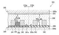
図3は、図2におけるA−A断面に沿った構成を示す図である。図中左側が図2における上側の構成(共通電極線の一部の断面構成)に対応しており、図中右側が図2における下側の構成(走査線の断面構成)に対応している。図2には示されていないが、図3にはカラーフィルタ基板5を含めた断面構成を示している。 FIG. 3 is a diagram showing a configuration along the section AA in FIG. The left side in the drawing corresponds to the upper configuration in FIG. 2 (partial cross-sectional configuration of the common electrode line), and the right side in the drawing corresponds to the lower configuration in FIG. 2 (cross-sectional configuration of the scanning line). . Although not shown in FIG. 2, FIG. 3 shows a cross-sectional configuration including the
同図に示すように、TFTアレイ基板4は、例えばガラスや石英、プラスチックなどの光透過可能な材料からなる矩形の基材4aを主体として構成されている。基材4a上には図示しない下地層が形成されている。下地層上の一部の領域には上記の走査線44が形成されている。この下地層上には、ゲート絶縁層49が設けられている。ゲート絶縁層49は、例えばSiO2やSiNなどの絶縁材料からなる層間絶縁膜であり、走査線44上を含めた下地層のほぼ全面を覆っている。 As shown in the figure, the
ゲート絶縁層49上には、上記の半導体薄膜47と、ソース電極45aと、ドレイン電極47dとが形成されている。半導体薄膜47は、ゲート絶縁層49を挟んで走査線44に対向するように配置されている。半導体薄膜47、ゲート絶縁層49及び走査線44によって、バックゲート型のTFT(Thin Film Transistor)が構成されている。このTFTにおいて、走査線44のうち半導体薄膜47に平面視で重なる領域は、ゲート電極として機能している。 On the
ソース電極45aは、一部が半導体薄膜47のソース領域47b上を覆うように形成されている。ソース電極45aと同じ層内には上記のデータ線45(図3には示していない)も形成されている。ゲート絶縁層49上には樹脂層50が設けられている。樹脂層50は、半導体薄膜47、ソース電極45a、ドレイン電極47d及びデータ線45を含めたゲート絶縁層49上のほぼ全面を覆っている。 The source electrode 45 a is formed so as to partially cover the
樹脂層50の一部には凹部50bが設けられている。この凹部50b内には、上記の光反射層41が設けられている。光反射層41の上面41aと樹脂層50の上面50aとの間は平坦になっている。この上面41aと上面50aとで一つの基板面を構成している。樹脂層50のうちドレイン電極47dに平面視で重なる領域には、当該樹脂層50を貫通するようにコンタクトホール47eが設けられている。 A
光反射層41の上面41a及び樹脂層50の上面50aには、画素電極42と共通電極43とがそれぞれ設けられている。樹脂層50のうちコンタクトホール47eに平面視で重なる領域には、画素電極42のコンタクト部42bが配置されている。コンタクトホール47eはコンタクト部42bを構成する導電材料によって埋められており、コンタクト部42bとコンタクトホール47e内に埋められた部分とが一体的になっている。コンタクトホール47eに埋められた部分の先端(図中下側)は、ドレイン電極47dに当接している。当該当接部においてコンタクト部42bとドレイン電極47dとが電気的に接続されている。 A
画素電極42及び共通電極43は、反射表示領域10aと透過表示領域10bとで比べると、基板面からの高さ(厚さ)が異なっている。反射表示領域10aでは、画素電極42及び共通電極43の厚さは0.40μm程度に形成されている。透過表示領域10bでは、画素電極42及び共通電極43の厚さは0.72μm程度に形成されている。このように、透過表示領域10b内の画素電極42及び共通電極43の厚さは、反射表示領域10a内の画素電極42及び共通電極43の厚さに比べて厚くなっており、具体的には1.8倍程度の厚さになっている。反射表示領域10a及び透過表示領域10bにおいて、画素電極42及び共通電極43の厚さはそれぞれ変更可能である。 The
反射表示領域10a内又は透過表示領域10b内だけで比較すると、画素電極42の厚さと共通電極43の厚さはほぼ同一の厚さになっている。画素電極42各部位(基端部42a、コンタクト部42b、枝状部42c)及び共通電極43の各部位(基端部43a、コンタクト部43b、枝状部43c)は、反射表示領域10a内及び透過表示領域10b内で、それぞれ同一の厚さになっている。 Comparing only in the
基材4aの外面上には、位相差板21が設けられている。位相差板21は、透過光に対して略1/4波長の位相差を付与するλ/4位相差板である。位相差板21には所定の方向に遅相軸が形成されている。 A
位相差板21の外面上には偏光板22が設けられている。偏光板22は、位相差板21の遅相軸に対して約45°の角度をなす方向に偏光軸が形成されている。位相差板21及び偏光板22によって円偏光板23が構成されている。円偏光板23としては、位相差板21及び偏光板22を組み合わせる構成の他、偏光板とλ/2位相差板とλ/4位相差板とを組み合わせた広帯域円偏光板であっても構わない。 A
一方、カラーフィルタ基板5は、TFTアレイ基板4と同様、例えばガラスや石英、プラスチックなどの光透過可能な材料からなる矩形の基材5aを主体として構成されている。基材5aの内面(TFTアレイ基板4との対向面)には、カラーフィルタ層51と、ブラックマトリクス52とが設けられている。 On the other hand, the
カラーフィルタ層51は、平面視でサブ画素領域10に重なる位置に設けられた色層である。カラーフィルタ層51は、例えば有機材料や無機材料など公知の材料からなる赤色層、緑色層、青色層の3色の色層からなる。上記赤色層は、平面視で赤色サブ画素に重なる領域に設けられている。上記緑色層は、平面視で緑色サブ画素に重なる領域に設けられている。上記青色層は、平面視で青色サブ画素に重なる領域に設けられている。ブラックマトリクス52は、画素間領域11に設けられており、光を吸収する例えばクロムなどの材料からなる。 The
基材5aの外面上には、位相差板31が設けられている。位相差板31は、位相差板21と同様、透過光に対して略1/4波長の位相差を付与するλ/4位相差板である。位相差板31には所定の方向に遅相軸が形成されている。 A
位相差板31の外面上には偏光板32が設けられている。偏光板32は、位相差板31の遅相軸に対して約45°の角度をなす方向に偏光軸が形成されている。位相差板31及び偏光板32によって円偏光板33が構成されている。円偏光板33としては、偏光板とλ/2位相差板とλ/4位相差板とを組み合わせた広帯域円偏光板であっても構わない。 A
液晶層6は、TFTアレイ基板4とカラーフィルタ基板5との双方に接するように挟持されている。この液晶層6は、電界の非印加時に光学的に等方性を示すと共に、電界の印加時には電界強度の2乗に比例する光学異方性を示す(Kerr効果)液晶材料からなる。このような液晶材料として、例えばブルー相の液晶材料が挙げられる。液晶層6の液晶分子の誘電率は正(ε>0)になっている。 The
ブルー相は、キラルネマチック相と等方相の間の狭い温度範囲に現れる、光学的に等方性の液晶相である。ブルー相の液晶材料には、例えばKerr効果の発現温度範囲の狭い(1K程度)液晶分子と少量の高分子とが含まれている(高分子安定化ブルー相)。液晶分子と共に高分子を含ませることにより、当該発現温度範囲が100K程度になっている。 The blue phase is an optically isotropic liquid crystal phase that appears in a narrow temperature range between the chiral nematic phase and the isotropic phase. The liquid crystal material of the blue phase contains, for example, a liquid crystal molecule having a narrow Kerr effect temperature range (about 1K) and a small amount of polymer (polymer-stabilized blue phase). By including a polymer together with liquid crystal molecules, the expression temperature range is about 100K.
高分子安定化ブルー相は、[数1]に示されるように、リタデーションの大きさ(Δn)が電界の2乗に比例する。[数1]において、KはKerr係数、λは光の波長、Eは電極間に生じる電界を示している。高分子安定化ブルー相のKerr係数は3.7×10⁻¹⁰(mV−2)であり、ニトロベンゼンの約170倍の大きさとなっている。 In the polymer-stabilized blue phase, as shown in [Equation 1], the magnitude of retardation (Δn) is proportional to the square of the electric field. In [Equation 1], K is the Kerr coefficient, λ is the wavelength of light, and E is the electric field generated between the electrodes. The Kerr coefficient of the polymer-stabilized blue phase is 3.7 × 10 −10 (mV−2), which is about 170 times that of nitrobenzene.

高分子安定化ブルー相の立ち上り(Kerr効果の発現)の応答時間及び立ち下り(Kerr効果の消滅)の応答時間は、いずれも10〜100μs程度である。一般的なネマチック液晶の応答時間は10ms程度である。高分子安定化ブルー相の応答は、一般的なネマチック液晶の応答に比べて格段に速くなっている。 The response time for the rise (expression of the Kerr effect) and the response time for the fall (disappearance of the Kerr effect) of the polymer-stabilized blue phase are both about 10 to 100 μs. A typical nematic liquid crystal has a response time of about 10 ms. The response of the polymer-stabilized blue phase is much faster than that of a general nematic liquid crystal.
バックライト3は、公知の構成となっている。具体的には、LEDなどの光源部と、アクリル樹脂などの透明な材料からなる導光板と、当該導光板に対して液晶パネル2側に設けられた拡散板と、拡散板の液晶パネル側2に設けられた集光板とを主体として構成されている。 The backlight 3 has a known configuration. Specifically, a light source unit such as an LED, a light guide plate made of a transparent material such as acrylic resin, a diffusion plate provided on the
(液晶表示装置の動作)
本実施形態の液晶表示装置1の動作について説明する。
まず、透過表示(透過モード)について説明する。
バックライト3から射出された光は、偏光板22および位相差板21を透過する過程で円偏光に変換される。円偏光に変換された光は、TFTアレイ基板4を透過して液晶層6に入射する。ブルー相が電圧無印加時に光学的に等方性を示すことから、液晶層6に入射した光は、光学異方性の影響を受けることなく円偏光のまま液晶層6を透過する。液晶層6を透過した光は、カラーフィルタ基板5を透過し、位相差板31に入射する。この光は、位相差板31を透過する過程で偏光板32の透過軸と直交する直線偏光に変換される。この直線偏光は偏光板32を透過しないので、電圧無印加時には黒表示となる(ノーマリーブラック表示)。(Operation of liquid crystal display)
The operation of the liquid
First, transmissive display (transmission mode) will be described.
Light emitted from the backlight 3 is converted into circularly polarized light in the process of passing through the
画素電極42と共通電極43との間に電圧を印加すると、液晶層6は光学異方性を呈する。バックライト3から射出された光は、偏光板32及び位相差板31を透過して円偏光に変換される。この光は、液晶層6に入射し、液晶層6を透過する過程で回転方向が反転した楕円偏光に変換される。この光は、位相差板31に入射し、偏光板32の透過軸と略平行の直線偏光に変換され、位相差板31を透過する。位相差板31を透過した光は、その全部または一部が偏光板32を透過する。このように、電圧印加時には白表示となる。 When a voltage is applied between the
次に、反射表示(反射モード)について説明する。
偏光板32の外面に入射した外光は、当該偏光板32及び位相差板31を透過する過程で円偏光に変換される。円偏光に変換された光は、カラーフィルタ基板5を透過して液晶層6に入射する。ブルー相が電圧無印加時に光学的に等方性を示すことから、液晶層6に入射した光は、光学異方性の影響を受けることなく円偏光のまま液晶層6を透過する。液晶層6を透過した光は、光反射層41により反射され、反射時に回転方向が反転する。反射光は、回転方向が反転した状態で、光学異方性の影響を受けることなく円偏光のままカラーフィルタ基板5へ向けて液晶層6を透過する。この光はカラーフィルタ基板5を透過して、位相差板31に入射する。位相差板31を透過する際、偏光板32の透過軸と直交する直線偏光に変換される。この直線偏光は偏光板32を透過できないので、電圧無印加時には黒表示となる(ノーマリーブラック表示)。Next, reflection display (reflection mode) will be described.
External light incident on the outer surface of the
画素電極42と共通電極43との間に電圧を印加すると、液晶層6は光学異方性を呈する。偏光板32の外面に入射した外光は、当該偏光板32及び位相差板31を透過する過程で円偏光に変換される。円偏光に変換された光は、カラーフィルタ基板5を透過して液晶層6に入射する。この光は、液晶層6を透過する過程で所定の位相差(λ/4)が付与されて光反射層41で反射される。光反射層41で反射された後、液晶層6をカラーフィルタ基板5へ向けて透過する際に、再度所定の位相差(λ/4)が付与される。液晶層6を透過した光は、カラーフィルタ基板5を透過し、位相差板31に入射する。光は位相差板31を透過する過程で、偏光板32の透過軸と平行な直線偏光に変換される。位相差板31を透過した光は、その全部または一部が偏光板32を透過する。このように、電圧印加時には白表示となる。 When a voltage is applied between the
リタデーションの大きさは、液晶層6の厚さ(d)と光学異方性(Δn)との積(Δnd)で規定される。反射表示領域10aと透過表示領域10bとが設けられたいわゆる半透過反射型の液晶表示装置1において、光は反射表示領域10a内の液晶層6を2回通過する。このことは、反射表示領域10aの液晶層6の厚さが透過表示領域10bの液晶層6の厚さの2倍であることと等価である。したがって、マルチギャップを採用しない構成では、反射表示領域10aのリタデーションは透過表示領域10bのリタデーションの2倍になる。これに対して、透過表示領域10bのリタデーションを高めることによって、透過表示領域10bのリタデーションを反射表示領域10aのリタデーション同等にすることができる。 The magnitude of the retardation is defined by the product (Δnd) of the thickness (d) of the
本実施形態によれば、透過表示領域10bでは反射表示領域10aに比べて、画素電極42及び共通電極43の基板面からの高さが高いので、その分画素電極42と共通電極43とで挟まれた部分の液晶層6に印加される電界の範囲を広くすることができる。したがって、透過表示領域10bの画素電極42と共通電極43とで挟まれた部分の液晶層6には、より強い電界を印加することができる。 According to the present embodiment, the
このように、本実施形態によれば、液晶層6の光学異方性が電界の2乗に比例して大きくなるので、透過表示領域10bの液晶層6に反射表示領域10aの液晶層6よりも強い電界を印加することにより、透過表示領域10bの光学異方性が反射表示領域10aの光学異方性よりも大きくなる。このため、透過表示領域10bのリタデーションを高めることができる。透過表示領域10bのリタデーションを高めることにより、当該透過表示領域10bのリタデーションを反射表示領域のリタデーションと同等にすることができ、反射表示領域10aと透過表示領域10bとの間の光透過率の差を解消することができる。これにより、反射表示領域10aと透過表示領域10bとの間のコントラストの差を解消することができ、表示特性の高い液晶表示装置1を得ることができる。 As described above, according to the present embodiment, the optical anisotropy of the
図4は、本実施形態の液晶表示装置1について画素電極42と共通電極43との間に印加される電圧の大きさ(V)と、液晶層6の光透過率の大きさ(相対値)との関係を示すグラフである。グラフの縦軸が光透過率の大きさを示している。グラフの横軸が電圧の大きさを示している。同グラフ中では、反射表示領域10aの液晶層6の光透過率を実線で示しており、透過表示領域10bの液晶層6の光透過率を破線で示している。 FIG. 4 shows the magnitude (V) of the voltage applied between the
同図に示すように、画素電極42と共通電極43との間に印加される電圧の大きさが6Vを超える範囲で反射表示領域10aの光透過率の値と透過表示領域10bの光透過率の値とが近似している。電圧の大きさが8V〜12Vの範囲では、両領域の光透過率の値は極めて近くなる。特に、電圧の値が9V〜10Vの範囲では、両領域の光透過率の値がほぼ一致する。 As shown in the figure, the value of the light transmittance of the
上記の電圧値は、反射表示領域10aで画素電極42及び共通電極43の厚さが0.40μm程度に形成されていると共に透過表示領域10bで画素電極42及び共通電極43の厚さは0.72μm程度に形成されている場合の値である。反射表示領域10a及び透過表示領域10bにおいて、画素電極42及び共通電極43の厚さはそれぞれ変更可能である。画素電極42及び共通電極43の厚さを変更することにより、上記電圧値を変化させることができる。本実施形態では、反射表示領域10aのリタデーション(Δnd)がλ/4となり、透過表示領域10bのリタデーションがλ/2となるように画素電極42及び共通電極43の厚さが調節されている。 The voltage values described above are such that the
本実施形態の液晶表示装置1の構成においては、画素電極42と共通電極43との間に等電圧を印加した場合に、反射表示領域10aの光透過率と透過表示領域10bの光透過率とが同等になるような電圧の範囲が出現することになる。したがって、液晶表示装置1を駆動する場合、この両領域の光透過率が同等になる範囲内で電圧を印加することにより、両領域の光透過率を同等とすることができ、両領域で同等のコントラストを得ることができる。 In the configuration of the liquid
[第2実施形態]
次に、本発明の第2実施形態を説明する。
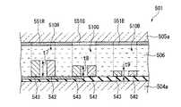
図5は、本実施形態に係る液晶表示装置101の構成を示す断面図である。同図は、第1実施形態における図3に対応している。本実施形態の液晶表示装置101は、カラーフィルタ基板及び液晶層の構成が第1実施形態と同様であり、TFTアレイ基板の構成が第1実施形態とは異なっている。[Second Embodiment]
Next, a second embodiment of the present invention will be described.
FIG. 5 is a cross-sectional view showing the configuration of the liquid
図5に示すように、画素電極142及び共通電極143は、TFTアレイ基板104側に設けられている。反射表示領域110aでは、画素電極(第3電極)142及び共通電極(第4電極)143が光反射層141の表面141aに直接設けられている。透過表示領域110bでは、樹脂層150の表面150a上に絶縁層155が設けられており、当該絶縁層155上に画素電極(第1電極)142及び共通電極(第2電極)143が設けられている。反射表示領域110a側の画素電極142及び共通電極143と、透過表示領域110b側の画素電極142及び共通電極143とは一体的に形成されている。勿論、画素電極142及び共通電極143が各領域ごとに分離されていても構わない。 As shown in FIG. 5, the
反射表示領域110a内の画素電極142及び共通電極143の厚さ、透過表示領域110b内の画素電極142及び共通電極143の厚さは、共に0.4μm程度と同一になっている。画素電極142及び共通電極143の配列のピッチは8μm程度であり、それぞれの電極幅は8μm程度である。 The thickness of the
絶縁層155は、電気的に絶縁性を有する材料、例えばSiO2やSiNなどの無機材料や、樹脂などの有機材料からなる。絶縁層155の厚さは2μm程度である。透過表示領域110bでは、この絶縁層155の厚さ分、画素電極142及び共通電極143がよりカラーフィルタ基板105側(基板面(樹脂層150の表面150a)からの高さが高い位置)に設けられている。 The insulating
液晶層106の層厚は一定になっている。液晶層106のうち画素電極142と共通電極143とで挟まれた部分の厚さは等しくなっている。当該部分の厚さ方向の中央部Mから反射表示領域110a内の画素電極142及び共通電極143までの距離t1は、当該中央部Mから透過表示領域110b内の画素電極142及び共通電極143までの距離t2よりも大きくなっている(t1>t2)。
その他の構成は、第1実施形態に係る液晶表示装置1と同様の構成になっている。The layer thickness of the
Other configurations are the same as those of the liquid
このように、本実施形態では、透過表示領域110bでは反射表示領域110aに比べて、画素電極142及び共通電極143がよりカラーフィルタ基板105側に設けられているので、透過表示領域110bの方が画素電極142及び共通電極143から液晶層106の中央部Mまでの厚さ方向の距離がより小さくなり(t1>t2)、液晶層106の中央部により近い位置に画素電極142及び共通電極143が配置されることになる。このため、画素電極142と共通電極143とで挟まれた部分の液晶層106には、両電極142、143の上下方向に亘って広い範囲に電界を印加することができる。したがって、透過表示領域110bの液晶層106には、反射表示領域110aの液晶層106に比べて、より強い電界が印加されることになる。当該透過表示領域110bのリタデーションを反射表示領域110aのリタデーションと同等にすることができ、反射表示領域110aと透過表示領域110bとの間の光透過率の差を解消することができる。これにより、反射表示領域110aと透過表示領域110bとの間のコントラストの差を解消することができ、表示特性の高い液晶表示装置101を得ることができる。 Thus, in this embodiment, since the
図6は、本実施形態の液晶表示装置101について画素電極142と共通電極143との間に印加される電圧の大きさ(V)と、液晶層106の光透過率の大きさ(相対値)との関係を示すグラフである。グラフの縦軸が光透過率の大きさを示している。グラフの横軸が電圧の大きさを示している。同グラフ中では、反射表示領域110aの液晶層106の光透過率を実線で示しており、透過表示領域110bの液晶層106の光透過率を破線で示している。 6 shows the magnitude (V) of the voltage applied between the
同図に示すように、画素電極142と共通電極43との間に印加される電圧の大きさが6Vを超える範囲で反射表示領域110aの光透過率の値と透過表示領域110bの光透過率の値とが近似している。電圧の大きさが7V〜12Vの範囲では、両領域の光透過率の値は極めて近くなる。特に、電圧の値が8V〜10Vの範囲では、両領域の光透過率の値がほぼ一致する。 As shown in the figure, the value of the light transmittance of the
上記の電圧値は、反射表示領域110aで画素電極142及び共通電極143の厚さが0.40μm程度に形成されていると共に透過表示領域110bの絶縁層155の厚さが2μm程度に形成されている場合の値である。反射表示領域110a及び透過表示領域110bにおける画素電極42及び共通電極43の厚さ、透過表示領域110bにおける絶縁層155の厚さなどはそれぞれ変更可能である。これらの値を変更することにより、上記電圧値を変化させることができる。本実施形態では、反射表示領域110aのリタデーション(Δnd)がλ/4となり、透過表示領域110bのリタデーションがλ/2となるように画素電極142及び共通電極143の厚さが調節されている。 In the
本実施形態の液晶表示装置101の構成においては、画素電極142と共通電極143との間に等電圧を印加した場合に、反射表示領域110aの光透過率と透過表示領域110bの光透過率とが同等になるような電圧の範囲が出現することになる。したがって、液晶表示装置101を駆動する場合、この両領域の光透過率が同等になる範囲内で電圧を印加することにより、両領域の光透過率を同等とすることができ、両領域で同等のコントラストを得ることができる。 In the configuration of the liquid
[第3実施形態]
次に、本発明の第3実施形態を説明する。
図7は、本実施形態に係る液晶表示装置201の構成を示す断面図である。同図は、第1実施形態における図3に対応している。本実施形態の液晶表示装置201は、カラーフィルタ基板及び液晶層の構成が第1実施形態と同様であり、TFTアレイ基板の構成が第1実施形態とは異なっている。[Third Embodiment]
Next, a third embodiment of the present invention will be described.
FIG. 7 is a cross-sectional view showing the configuration of the liquid
図7に示すように、画素電極242及び共通電極243は、TFTアレイ基板204側に設けられている。反射表示領域210aでは、画素電極(第3電極)242及び共通電極(第4電極)243が光反射層241の表面241aに設けられている。透過表示領域210bでは、画素電極(第1電極)242及び共通電極(第2電極)243が樹脂層250の表面250a上に設けられている。反射表示領域210a側の画素電極242及び共通電極243と、透過表示領域210b側の画素電極242及び共通電極243とは一体的に形成されている。勿論、画素電極242及び共通電極243が各領域ごとに分離されていても構わない。 As shown in FIG. 7, the
反射表示領域210a内の画素電極242及び共通電極243の厚さ、透過表示領域210b内の画素電極242及び共通電極243の厚さは、共に0.4μm程度と同一になっている。画素電極242及び共通電極243の配列のピッチは8μm程度であり、それぞれの電極幅は8μm程度である。 The thicknesses of the
透過表示領域210bでは、樹脂層250のうち画素電極242と共通電極243とで挟まれた領域に凹部255が設けられている。凹部255は、画素電極242と共通電極243との間の距離と同一の幅を有しており、その深さ(樹脂層250の表面250aから底部までの距離)が凹部255の全体でほぼ2.5μm程度と均一になっている。反射表示領域210aでは、光反射層241の表面241aが液晶層206との界面になっている。透過表示領域210bでは、この凹部255の底部が液晶層206との界面になっている。したがって、透過表示領域210bでは反射表示領域210aに比べて、画素電極242と共通電極243とで挟まれる部分の液晶層206の厚さが大きくなる。 In the
図7中に、反射表示領域210aの液晶層206のうち画素電極242と共通電極243とで挟まれる部分の厚さ方向の中央部(反射側中央部)をMrで示し、透過表示領域210bの当該中央部(透過側中央部)をMtで示す。反射側中央部Mrは、透過側中央部Mtよりもカラーフィルタ基板205側に位置することになる。したがって、反射側中央部Mrから反射表示領域210a内の画素電極242及び共通電極243までの距離t3は、透過側中央部Mtから透過表示領域210b内の画素電極242及び共通電極243までの距離t4よりも大きくなっている(t3>t4)。
その他の構成は、第1実施形態に係る液晶表示装置1と同様の構成になっている。In FIG. 7, in the
Other configurations are the same as those of the liquid
このように、本実施形態では、樹脂層250のうち画素電極242と共通電極243とで挟まれた領域に凹部255が設けられているので、反射側中央部Mrから反射表示領域210a内の画素電極242及び共通電極243までの距離t3が、透過側中央部Mtから透過表示領域210b内の画素電極242及び共通電極243までの距離t4よりも大きくなり(t3>t4)、透過表示領域210bの方が中央部(透過側中央部Mt)に近い位置に画素電極242及び共通電極243が配置されることになる。このため、画素電極242と共通電極243とで挟まれた部分の液晶層206には、両電極242、243の上下方向に亘って広い範囲に電界を印加することができる。したがって、透過表示領域210bの液晶層206には、反射表示領域210aの液晶層206に比べて、より強い電界が印加されることになる。当該透過表示領域210bのリタデーションを反射表示領域210aのリタデーションと同等にすることができるので、反射表示領域210aと透過表示領域210bとの間の光透過率の差を解消することができる。これにより、反射表示領域210aと透過表示領域210bとの間のコントラストの差を解消することができ、表示特性の高い液晶表示装置201を得ることができる。 Thus, in this embodiment, since the recessed
[第4実施形態]
次に、本発明の第4実施形態を説明する。
図8は、本実施形態に係る液晶表示装置301の構成を示す断面図である。同図は、第1実施形態における図3を簡略化して示している。本実施形態の液晶表示装置301は、カラーフィルタ基板及び液晶層の構成が第1実施形態と同様であり、TFTアレイ基板の構成が第1実施形態とは異なっている。[Fourth Embodiment]
Next, a fourth embodiment of the present invention will be described.
FIG. 8 is a cross-sectional view showing the configuration of the liquid
図8に示すように、画素電極342及び共通電極343は、TFTアレイ基板304側に設けられている。反射表示領域310aでは、画素電極(第3電極)342及び共通電極(第4電極)343が光反射層341の表面341aに設けられている。透過表示領域310bでは、画素電極(第1電極)342及び共通電極(第2電極)343が樹脂層350の表面350a上に設けられている。反射表示領域310a側の画素電極342及び共通電極343と、透過表示領域310b側の画素電極342及び共通電極343とは一体的に形成されている。勿論、画素電極342及び共通電極343が各領域ごとに分離されていても構わない。 As shown in FIG. 8, the
反射表示領域310a内の画素電極342及び共通電極343の厚さ、透過表示領域310b内の画素電極342及び共通電極343の厚さは、共に0.4μm程度と同一になっている。画素電極342及び共通電極343の配列のピッチは8μm程度であり、それぞれの電極幅は8μm程度である。 The thickness of the
反射表示領域310aでは、光反射層341の表面341a上のうち画素電極342と共通電極343とで挟まれた領域に凸部355が設けられている。凸部355は、画素電極342と共通電極343との間を一部埋めるように設けられている。反射表示領域310aでは、凸部355の表面が液晶層306との界面になっている。透過表示領域310bでは、樹脂層350の表面350aが液晶層306との界面になっている。したがって、透過表示領域310bでは反射表示領域310aに比べて、画素電極342と共通電極343とで挟まれる部分の液晶層306の厚さが大きくなる。 In the
図8中に、反射表示領域310aの液晶層306のうち画素電極342と共通電極343とで挟まれる部分の厚さ方向の中央部(反射側中央部)をMrで示し、透過表示領域310bの当該中央部(透過側中央部)をMtで示す。反射側中央部Mrは、透過側中央部Mtよりもカラーフィルタ基板305側に位置することになる。したがって、反射側中央部Mrから反射表示領域310a内の画素電極342及び共通電極343までの距離t5は、透過側中央部Mtから透過表示領域310b内の画素電極342及び共通電極343までの距離t6よりも大きくなっている(t5>t6)。
その他の構成は、第1実施形態に係る液晶表示装置1と同様の構成になっている。In FIG. 8, the central portion in the thickness direction (reflective side central portion) of the portion sandwiched between the
Other configurations are the same as those of the liquid
このように、本実施形態では、反射表示領域310aにおいて光反射層341の表面341a上のうち画素電極342と共通電極343とで挟まれた領域に凸部355が設けられているので、反射側中央部Mrから反射表示領域310a内の画素電極342及び共通電極343までの距離t5が、透過側中央部Mtから透過表示領域310b内の画素電極342及び共通電極343までの距離t6よりも大きくなり(t5>t6)、透過表示領域310bの方が中央部(透過側中央部Mt)に近い位置に画素電極342及び共通電極343が配置されることになる。これにより、上記実施形態と同様に、反射表示領域310aと透過表示領域310bとの間のコントラストの差を解消することができ、表示特性の高い液晶表示装置301を得ることができる。 As described above, in the present embodiment, the
[第5実施形態]
次に、本発明の第5実施形態を説明する。
図9は、本実施形態に係る液晶表示装置401の構成を示す断面図である。同図は、第1実施形態における図3を簡略化して示している。本実施形態の液晶表示装置401は、カラーフィルタ基板の構成が第1実施形態と同様であり、TFTアレイ基板の構成が第1実施形態とは異なっている。本実施形態では、液晶層406の液晶分子の誘電率が負(ε<0)になっている点でも、第1実施形態とは異なっている。[Fifth Embodiment]
Next, a fifth embodiment of the present invention will be described.
FIG. 9 is a cross-sectional view showing the configuration of the liquid
図9に示すように、画素電極442及び共通電極443は、TFTアレイ基板404側に設けられている。反射表示領域410aでは、画素電極(第3電極)442及び共通電極(第4電極)443が光反射層441の表面441aに設けられている。透過表示領域410bでは、画素電極(第1電極)442及び共通電極(第2電極)443が樹脂層450の表面450a上に設けられている。反射表示領域410a側の画素電極442及び共通電極443と、透過表示領域410b側の画素電極442及び共通電極443とは一体的に形成されている。勿論、画素電極442及び共通電極443が各領域ごとに分離されていても構わない。 As shown in FIG. 9, the
反射表示領域410a内では、画素電極442の厚さと共通電極443の厚さとが異なっている。具体的には、画素電極442の厚さよりも共通電極443の方が厚くなっている。透過表示領域310b内でも、画素電極442の厚さと共通電極443の厚さとが異なっており、画素電極442の厚さよりも共通電極443の方が厚くなっている。画素電極342及び共通電極343の配列のピッチは8μm程度であり、それぞれの電極幅は8μm程度である。 In the
このように、本実施形態によれば、液晶層406が電界に対して負の誘電率異方性(ε<0)を示す部分では、画素電極442の厚さ方向の寸法が共通電極443の厚さ方向の寸法よりも小さくなっているので、負の誘電率異方性を示す部分の液晶分子の配向を所望の方向に規制することができる。 As described above, according to the present embodiment, in the portion where the
[第6実施形態]
次に、本発明の第6実施形態を説明する。
図10は、本実施形態に係る液晶表示装置501の構成を示す断面図である。本実施形態の液晶表示装置501は、カラーフィルタ基板の構成が第1実施形態と同様であり、TFTアレイ基板の構成が第1実施形態とは異なっている。[Sixth Embodiment]
Next, a sixth embodiment of the present invention will be described.
FIG. 10 is a cross-sectional view showing the configuration of the liquid
図10に示すように、画素電極542及び共通電極543は、TFTアレイ基板504側に設けられている。当該画素電極542及び共通電極543は、赤色カラーフィルタ層551Rが設けられた赤色サブ画素510Rと、緑色カラーフィルタ層551Gが設けられた緑色サブ画素510Gと、青色カラーフィルタ層551Bが設けられた青色サブ画素510Bとの間で、それぞれ基板面550aからの高さ(厚さ)が異なっている。具体的には、赤色サブ画素510R内での高さをt7、緑色サブ画素510G内での高さをt6、青色サブ画素510B内での高さをt9とすると、t7>t8>t9となっており、赤色サブ画素510R、緑色サブ画素510G、青色サブ画素510Bの順に画素電極542及び共通電極543の高さが小さくなっている。 As shown in FIG. 10, the
このように、本実施形態によれば、赤色サブ画素510R、緑色サブ画素510G、青色サブ画素510Bの順に画素電極542及び共通電極543の高さが小さくなっているので、色光の種類に応じて最適な光透過率を得ることができる。これにより、表示特性の高い液晶表示装置501を得ることができる。 As described above, according to the present embodiment, the height of the
[第7実施形態]
次に、本発明の第7実施形態を説明する。
図6は、本実施形態に係る電子機器(携帯電話)の全体構成を示す斜視図である。
携帯電話600は、筺体601、複数の操作ボタンが設けられた操作部602、画像や動画、文字等を表示する表示部603を有する。上記の表示部603には、本実施形態に係る液晶表示装置1〜501が搭載されている。
このように、透過表示領域及び反射表示領域にて同等の光透過率が得られ、コントラストの高い表示が可能な液晶表示装置1〜501を搭載したので、表示品位が高く、信頼性の高い携帯電話600を得ることができる。[Seventh Embodiment]
Next, a seventh embodiment of the present invention will be described.
FIG. 6 is a perspective view showing the overall configuration of the electronic apparatus (mobile phone) according to the present embodiment.
The
As described above, since the liquid
本発明の技術範囲は上記実施形態に限定されるものではなく、本発明の趣旨を逸脱しない範囲で適宜変更を加えることができる。
上記実施形態においては、液晶層の構成をコレステリックブルー相を含んだ構成として説明したが、これに限られることは無い。例えば、スメクティックブルー相やキュービック相、スメクティックD相、ミセル相などの材料を含んだ構成としても構わない。The technical scope of the present invention is not limited to the above-described embodiment, and appropriate modifications can be made without departing from the spirit of the present invention.
In the above embodiment, the configuration of the liquid crystal layer has been described as a configuration including a cholesteric blue phase, but the configuration is not limited thereto. For example, it may be configured to include materials such as a smectic blue phase, a cubic phase, a smectic D phase, and a micelle phase.
上記実施形態においては、配向膜を設けない構成として説明したが、例えばTFTアレイ基板の液晶層との界面に配向膜を形成しても構わない。この場合、電界によって液晶分子の配向が変化する方向にラビング処理を施すのが好ましい。これにより、液晶分子の配向の変化を促進させることができる。 In the above embodiment, the configuration in which the alignment film is not provided has been described. However, for example, the alignment film may be formed at the interface with the liquid crystal layer of the TFT array substrate. In this case, it is preferable to perform a rubbing process in a direction in which the orientation of liquid crystal molecules changes due to an electric field. Thereby, the change in the alignment of the liquid crystal molecules can be promoted.
画素電極及び共通電極の構成及びその周辺部の構成については、上記各実施形態に記載した構成に限られるものではない。透過表示領域において画素電極と共通電極とで挟まれた部分の電気光学物質層に印加される電界の厚さ方向の範囲が、反射表示領域において画素電極と共通電極とで挟まれた部分の電気光学物質層に印加される電界の厚さ方向の範囲よりも大きくなるような構成であれば、他の構成であっても構わない。 The configuration of the pixel electrode and the common electrode and the configuration of the periphery thereof are not limited to the configurations described in the above embodiments. The range in the thickness direction of the electric field applied to the portion of the electro-optic material layer sandwiched between the pixel electrode and the common electrode in the transmissive display region is equal to the electrical portion of the portion sandwiched between the pixel electrode and the common electrode in the reflective display region. Any other configuration may be used as long as it is larger than the range of the electric field applied to the optical material layer in the thickness direction.
1〜501…液晶表示装置 2…液晶パネル 4…TFTアレイ基板 5…カラーフィルタ基板 6…液晶層 10…サブ画素領域 10a…反射表示領域 10b…透過表示領域 11…画素間領域 21、31…位相差板 22、32…偏光板 23、33…円偏光板 41…光反射層 42…画素電極 42a…基端部 42b…コンタクト部 42c…枝状部 43…共通電極 43a…基端部 43b…コンタクト部 43c…枝状部 50…樹脂層 50b…凹部 155…絶縁層 255…凹部 355…凸部 600…携帯電話 603…表示部 DESCRIPTION OF SYMBOLS 1-501 ... Liquid
Claims (9)
Translated fromJapanese前記電気光学物質層を成す電気光学物質は、電界の非印加時に光学的に等方性を示し、且つ電界の印加時には電界強度の2乗に比例する光学異方性を示すとともに、負の誘電率異方性を有し、 The electro-optic material forming the electro-optic material layer is optically isotropic when no electric field is applied, and exhibits optical anisotropy proportional to the square of the electric field strength when an electric field is applied, and has a negative dielectric property. Has anisotropy
前記透過表示領域には、前記一対の基板のうち一方の基板の前記電気光学物質層側に、第1電極と、前記一方の基板からの高さが前記第1電極よりも高く形成される第2電極と、が設けられ、In the transmissive display area, a first electrode and a height from the one substrate higher than that of the first electrode are formed on the electro-optic material layer side of one of the pair of substrates. Two electrodes,
前記反射表示領域には、前記一方の基板の前記電気光学物質層側に、第3電極と、前記一方の基板からの高さが前記第3電極よりも高く形成される第4電極と、が設けられ、The reflective display region includes a third electrode on the electro-optic material layer side of the one substrate, and a fourth electrode formed with a height higher than the third electrode from the one substrate. Provided,
前記第1電極と前記第2電極、及び前記第3電極と前記第4電極は、前記透過表示領域において前記第1電極と前記第2電極とで挟まれた前記電気光学物質層の層厚が、前記反射表示領域において前記第3電極と前記第4電極とで挟まれた前記電気光学物質層の層厚よりも厚くなるように形成される、The first electrode and the second electrode, and the third electrode and the fourth electrode have a thickness of the electro-optic material layer sandwiched between the first electrode and the second electrode in the transmissive display region. The reflective display region is formed to be thicker than the thickness of the electro-optic material layer sandwiched between the third electrode and the fourth electrode.
電気光学装置。 Electro-optic device.
前記第1サブ画素領域における前記一方の基板の表面からの前記第1電極及び前記第2電極の高さが、前記第2サブ画素領域における前記一方の基板の表面からの前記第1電極及び前記第2電極の高さよりも高く形成される、The height of the first electrode and the second electrode from the surface of the one substrate in the first sub-pixel region is such that the first electrode and the height from the surface of the one substrate in the second sub-pixel region are Formed higher than the height of the second electrode;
請求項1に記載の電気光学装置。The electro-optical device according to claim 1.
前記第1サブ画素領域における前記一方の基板の表面からの前記第3電極及び前記第4電極の高さが、前記第2サブ画素領域における前記一方の基板の表面からの前記第3電極及び前記第4電極の高さよりも高く形成される、 The heights of the third electrode and the fourth electrode from the surface of the one substrate in the first subpixel region are such that the third electrode from the surface of the one substrate in the second subpixel region Formed higher than the height of the fourth electrode;
請求項1または請求項2に記載の電気光学装置。The electro-optical device according to claim 1.
請求項1に記載の電気光学装置。The electro-optical device according to claim 1.
請求項1乃至請求項4のうちいずれか一項に記載の電気光学装置。The electro-optic material includes a cholesteric blue phase;
The electro-optical device according to claim 1 .
請求項1乃至請求項5のうちいずれか一項に記載の電気光学装置。The electro-optical device according to claim 1.
請求項1乃至請求項6のうちいずれか一項に記載の電気光学装置。The electro-optical device according to claim 1.
請求項7に記載の電気光学装置。The electro-optical device according to claim 7.
Priority Applications (1)
| Application Number | Priority Date | Filing Date | Title |
|---|---|---|---|
| JP2007078304AJP5110927B2 (en) | 2007-03-26 | 2007-03-26 | Electro-optical device and electronic apparatus |
Applications Claiming Priority (1)
| Application Number | Priority Date | Filing Date | Title |
|---|---|---|---|
| JP2007078304AJP5110927B2 (en) | 2007-03-26 | 2007-03-26 | Electro-optical device and electronic apparatus |
Publications (2)
| Publication Number | Publication Date |
|---|---|
| JP2008241789A JP2008241789A (en) | 2008-10-09 |
| JP5110927B2true JP5110927B2 (en) | 2012-12-26 |
Family
ID=39913272
Family Applications (1)
| Application Number | Title | Priority Date | Filing Date |
|---|---|---|---|
| JP2007078304AExpired - Fee RelatedJP5110927B2 (en) | 2007-03-26 | 2007-03-26 | Electro-optical device and electronic apparatus |
Country Status (1)
| Country | Link |
|---|---|
| JP (1) | JP5110927B2 (en) |
Families Citing this family (6)
| Publication number | Priority date | Publication date | Assignee | Title |
|---|---|---|---|---|
| KR101555497B1 (en)* | 2008-12-19 | 2015-09-25 | 삼성디스플레이 주식회사 | Image display method and display device realizing the same |
| TWI501319B (en) | 2008-12-26 | 2015-09-21 | Semiconductor Energy Lab | Semiconductor device and manufacturing method thereof |
| JP2011180303A (en)* | 2010-02-26 | 2011-09-15 | Hitachi Displays Ltd | Liquid crystal display device |
| JP5290225B2 (en)* | 2010-03-23 | 2013-09-18 | 株式会社ジャパンディスプレイ | Liquid crystal display |
| US9069202B2 (en) | 2011-03-11 | 2015-06-30 | Semiconductor Energy Laboratory Co., Ltd. | Liquid crystal display device |
| CN109283751A (en)* | 2018-10-24 | 2019-01-29 | 北京航空航天大学 | A single-cell thick transflective blue-phase liquid crystal display |
Family Cites Families (2)
| Publication number | Priority date | Publication date | Assignee | Title |
|---|---|---|---|---|
| JP4027941B2 (en)* | 2004-01-16 | 2007-12-26 | シャープ株式会社 | Display element and display device |
| JP4138759B2 (en)* | 2005-02-03 | 2008-08-27 | セイコーエプソン株式会社 | Liquid crystal display device and electronic device |
- 2007
- 2007-03-26JPJP2007078304Apatent/JP5110927B2/ennot_activeExpired - Fee Related
Also Published As
| Publication number | Publication date |
|---|---|
| JP2008241789A (en) | 2008-10-09 |
Similar Documents
| Publication | Publication Date | Title |
|---|---|---|
| JP4453694B2 (en) | Liquid crystal device and electronic device | |
| KR100760745B1 (en) | Liquid crystal display device and electronic apparatus | |
| JP4434166B2 (en) | Liquid crystal device and electronic device | |
| CN100412631C (en) | Liquid crystal device and electronic equipment | |
| KR100805512B1 (en) | Liquid Crystal Devices and Electronics | |
| JP5019848B2 (en) | Liquid crystal device and electronic device | |
| KR100630020B1 (en) | Liquid crystal display device and electronic apparatus | |
| CN100417981C (en) | Liquid crystal device and electronic equipment | |
| KR20080075064A (en) | Liquid crystal display and electronics | |
| KR101888516B1 (en) | Dual mode liquid crystal display device | |
| JP2011149967A (en) | Liquid crystal display device | |
| JP5110927B2 (en) | Electro-optical device and electronic apparatus | |
| US20110128458A1 (en) | Liquid crystal display device | |
| CN100485477C (en) | Liquid crystal display device and electronic apparatus | |
| KR20110083141A (en) | Liquid crystal display apparatus | |
| JP2009258332A (en) | Liquid crystal display device and electronic device | |
| JP4155276B2 (en) | Liquid crystal device and electronic device | |
| US8427616B2 (en) | Bistable chiral splay nematic mode crystal display device | |
| JP5044831B2 (en) | Electro-optical device and electronic apparatus | |
| JP2008241947A (en) | Electro-optical device and electronic apparatus | |
| JP2005257904A (en) | Liquid crystal display | |
| JP5202938B2 (en) | Liquid crystal display | |
| JP4894817B2 (en) | Liquid crystal device | |
| KR101688593B1 (en) | In-plane switching mode transflective type liquid crystal display device | |
| JP5242476B2 (en) | Liquid crystal display |
Legal Events
| Date | Code | Title | Description |
|---|---|---|---|
| A521 | Written amendment | Free format text:JAPANESE INTERMEDIATE CODE: A821 Effective date:20100104 | |
| A621 | Written request for application examination | Free format text:JAPANESE INTERMEDIATE CODE: A621 Effective date:20100104 | |
| A711 | Notification of change in applicant | Free format text:JAPANESE INTERMEDIATE CODE: A711 Effective date:20100526 | |
| RD02 | Notification of acceptance of power of attorney | Free format text:JAPANESE INTERMEDIATE CODE: A7422 Effective date:20100526 | |
| A977 | Report on retrieval | Free format text:JAPANESE INTERMEDIATE CODE: A971007 Effective date:20111222 | |
| A131 | Notification of reasons for refusal | Free format text:JAPANESE INTERMEDIATE CODE: A131 Effective date:20120110 | |
| A521 | Written amendment | Free format text:JAPANESE INTERMEDIATE CODE: A523 Effective date:20120302 | |
| A711 | Notification of change in applicant | Free format text:JAPANESE INTERMEDIATE CODE: A711 Effective date:20120330 | |
| TRDD | Decision of grant or rejection written | ||
| A01 | Written decision to grant a patent or to grant a registration (utility model) | Free format text:JAPANESE INTERMEDIATE CODE: A01 Effective date:20120918 | |
| A01 | Written decision to grant a patent or to grant a registration (utility model) | Free format text:JAPANESE INTERMEDIATE CODE: A01 | |
| A61 | First payment of annual fees (during grant procedure) | Free format text:JAPANESE INTERMEDIATE CODE: A61 Effective date:20121009 | |
| FPAY | Renewal fee payment (event date is renewal date of database) | Free format text:PAYMENT UNTIL: 20151019 Year of fee payment:3 | |
| R150 | Certificate of patent or registration of utility model | Ref document number:5110927 Country of ref document:JP Free format text:JAPANESE INTERMEDIATE CODE: R150 Free format text:JAPANESE INTERMEDIATE CODE: R150 | |
| R250 | Receipt of annual fees | Free format text:JAPANESE INTERMEDIATE CODE: R250 | |
| R250 | Receipt of annual fees | Free format text:JAPANESE INTERMEDIATE CODE: R250 | |
| R250 | Receipt of annual fees | Free format text:JAPANESE INTERMEDIATE CODE: R250 | |
| R250 | Receipt of annual fees | Free format text:JAPANESE INTERMEDIATE CODE: R250 | |
| LAPS | Cancellation because of no payment of annual fees |