JP5109403B2 - Semiconductor memory device and manufacturing method thereof - Google Patents
Semiconductor memory device and manufacturing method thereofDownload PDFInfo
- Publication number
- JP5109403B2 JP5109403B2JP2007042498AJP2007042498AJP5109403B2JP 5109403 B2JP5109403 B2JP 5109403B2JP 2007042498 AJP2007042498 AJP 2007042498AJP 2007042498 AJP2007042498 AJP 2007042498AJP 5109403 B2JP5109403 B2JP 5109403B2
- Authority
- JP
- Japan
- Prior art keywords
- region
- semiconductor substrate
- gate electrode
- polysilicon
- via plug
- Prior art date
- Legal status (The legal status is an assumption and is not a legal conclusion. Google has not performed a legal analysis and makes no representation as to the accuracy of the status listed.)
- Expired - Fee Related
Links
Images


Classifications
- G—PHYSICS
- G11—INFORMATION STORAGE
- G11C—STATIC STORES
- G11C11/00—Digital stores characterised by the use of particular electric or magnetic storage elements; Storage elements therefor
- G11C11/21—Digital stores characterised by the use of particular electric or magnetic storage elements; Storage elements therefor using electric elements
- G11C11/34—Digital stores characterised by the use of particular electric or magnetic storage elements; Storage elements therefor using electric elements using semiconductor devices
- G11C11/40—Digital stores characterised by the use of particular electric or magnetic storage elements; Storage elements therefor using electric elements using semiconductor devices using transistors
- G11C11/41—Digital stores characterised by the use of particular electric or magnetic storage elements; Storage elements therefor using electric elements using semiconductor devices using transistors forming static cells with positive feedback, i.e. cells not needing refreshing or charge regeneration, e.g. bistable multivibrator or Schmitt trigger
- G11C11/412—Digital stores characterised by the use of particular electric or magnetic storage elements; Storage elements therefor using electric elements using semiconductor devices using transistors forming static cells with positive feedback, i.e. cells not needing refreshing or charge regeneration, e.g. bistable multivibrator or Schmitt trigger using field-effect transistors only
- G—PHYSICS
- G11—INFORMATION STORAGE
- G11C—STATIC STORES
- G11C11/00—Digital stores characterised by the use of particular electric or magnetic storage elements; Storage elements therefor
- G11C11/21—Digital stores characterised by the use of particular electric or magnetic storage elements; Storage elements therefor using electric elements
- G11C11/34—Digital stores characterised by the use of particular electric or magnetic storage elements; Storage elements therefor using electric elements using semiconductor devices
- G11C11/40—Digital stores characterised by the use of particular electric or magnetic storage elements; Storage elements therefor using electric elements using semiconductor devices using transistors
- H—ELECTRICITY
- H01—ELECTRIC ELEMENTS
- H01L—SEMICONDUCTOR DEVICES NOT COVERED BY CLASS H10
- H01L21/00—Processes or apparatus adapted for the manufacture or treatment of semiconductor or solid state devices or of parts thereof
- H01L21/70—Manufacture or treatment of devices consisting of a plurality of solid state components formed in or on a common substrate or of parts thereof; Manufacture of integrated circuit devices or of parts thereof
- H01L21/71—Manufacture of specific parts of devices defined in group H01L21/70
- H01L21/768—Applying interconnections to be used for carrying current between separate components within a device comprising conductors and dielectrics
- H01L21/76801—Applying interconnections to be used for carrying current between separate components within a device comprising conductors and dielectrics characterised by the formation and the after-treatment of the dielectrics, e.g. smoothing
- H01L21/76802—Applying interconnections to be used for carrying current between separate components within a device comprising conductors and dielectrics characterised by the formation and the after-treatment of the dielectrics, e.g. smoothing by forming openings in dielectrics
- H01L21/76816—Aspects relating to the layout of the pattern or to the size of vias or trenches
- H—ELECTRICITY
- H01—ELECTRIC ELEMENTS
- H01L—SEMICONDUCTOR DEVICES NOT COVERED BY CLASS H10
- H01L21/00—Processes or apparatus adapted for the manufacture or treatment of semiconductor or solid state devices or of parts thereof
- H01L21/70—Manufacture or treatment of devices consisting of a plurality of solid state components formed in or on a common substrate or of parts thereof; Manufacture of integrated circuit devices or of parts thereof
- H01L21/71—Manufacture of specific parts of devices defined in group H01L21/70
- H01L21/768—Applying interconnections to be used for carrying current between separate components within a device comprising conductors and dielectrics
- H01L21/76838—Applying interconnections to be used for carrying current between separate components within a device comprising conductors and dielectrics characterised by the formation and the after-treatment of the conductors
- H01L21/76895—Local interconnects; Local pads, as exemplified by patent document EP0896365
- H—ELECTRICITY
- H10—SEMICONDUCTOR DEVICES; ELECTRIC SOLID-STATE DEVICES NOT OTHERWISE PROVIDED FOR
- H10B—ELECTRONIC MEMORY DEVICES
- H10B10/00—Static random access memory [SRAM] devices
- H—ELECTRICITY
- H10—SEMICONDUCTOR DEVICES; ELECTRIC SOLID-STATE DEVICES NOT OTHERWISE PROVIDED FOR
- H10B—ELECTRONIC MEMORY DEVICES
- H10B10/00—Static random access memory [SRAM] devices
- H10B10/12—Static random access memory [SRAM] devices comprising a MOSFET load element
- H—ELECTRICITY
- H10—SEMICONDUCTOR DEVICES; ELECTRIC SOLID-STATE DEVICES NOT OTHERWISE PROVIDED FOR
- H10B—ELECTRONIC MEMORY DEVICES
- H10B10/00—Static random access memory [SRAM] devices
- H10B10/18—Peripheral circuit regions
- H—ELECTRICITY
- H10—SEMICONDUCTOR DEVICES; ELECTRIC SOLID-STATE DEVICES NOT OTHERWISE PROVIDED FOR
- H10D—INORGANIC ELECTRIC SEMICONDUCTOR DEVICES
- H10D84/00—Integrated devices formed in or on semiconductor substrates that comprise only semiconducting layers, e.g. on Si wafers or on GaAs-on-Si wafers
- H10D84/01—Manufacture or treatment
- H10D84/0123—Integrating together multiple components covered by H10D12/00 or H10D30/00, e.g. integrating multiple IGBTs
- H10D84/0126—Integrating together multiple components covered by H10D12/00 or H10D30/00, e.g. integrating multiple IGBTs the components including insulated gates, e.g. IGFETs
- H10D84/0165—Integrating together multiple components covered by H10D12/00 or H10D30/00, e.g. integrating multiple IGBTs the components including insulated gates, e.g. IGFETs the components including complementary IGFETs, e.g. CMOS devices
- H—ELECTRICITY
- H10—SEMICONDUCTOR DEVICES; ELECTRIC SOLID-STATE DEVICES NOT OTHERWISE PROVIDED FOR
- H10D—INORGANIC ELECTRIC SEMICONDUCTOR DEVICES
- H10D84/00—Integrated devices formed in or on semiconductor substrates that comprise only semiconducting layers, e.g. on Si wafers or on GaAs-on-Si wafers
- H10D84/01—Manufacture or treatment
- H10D84/02—Manufacture or treatment characterised by using material-based technologies
- H10D84/03—Manufacture or treatment characterised by using material-based technologies using Group IV technology, e.g. silicon technology or silicon-carbide [SiC] technology
- H10D84/038—Manufacture or treatment characterised by using material-based technologies using Group IV technology, e.g. silicon technology or silicon-carbide [SiC] technology using silicon technology, e.g. SiGe
- H—ELECTRICITY
- H10—SEMICONDUCTOR DEVICES; ELECTRIC SOLID-STATE DEVICES NOT OTHERWISE PROVIDED FOR
- H10D—INORGANIC ELECTRIC SEMICONDUCTOR DEVICES
- H10D89/00—Aspects of integrated devices not covered by groups H10D84/00 - H10D88/00
- H10D89/10—Integrated device layouts
- H—ELECTRICITY
- H10—SEMICONDUCTOR DEVICES; ELECTRIC SOLID-STATE DEVICES NOT OTHERWISE PROVIDED FOR
- H10B—ELECTRONIC MEMORY DEVICES
- H10B10/00—Static random access memory [SRAM] devices
- H10B10/15—Static random access memory [SRAM] devices comprising a resistor load element
- H—ELECTRICITY
- H10—SEMICONDUCTOR DEVICES; ELECTRIC SOLID-STATE DEVICES NOT OTHERWISE PROVIDED FOR
- H10D—INORGANIC ELECTRIC SEMICONDUCTOR DEVICES
- H10D1/00—Resistors, capacitors or inductors
- H10D1/40—Resistors
- H10D1/47—Resistors having no potential barriers
- H—ELECTRICITY
- H10—SEMICONDUCTOR DEVICES; ELECTRIC SOLID-STATE DEVICES NOT OTHERWISE PROVIDED FOR
- H10D—INORGANIC ELECTRIC SEMICONDUCTOR DEVICES
- H10D84/00—Integrated devices formed in or on semiconductor substrates that comprise only semiconducting layers, e.g. on Si wafers or on GaAs-on-Si wafers
- H10D84/80—Integrated devices formed in or on semiconductor substrates that comprise only semiconducting layers, e.g. on Si wafers or on GaAs-on-Si wafers characterised by the integration of at least one component covered by groups H10D12/00 or H10D30/00, e.g. integration of IGFETs
- H10D84/811—Combinations of field-effect devices and one or more diodes, capacitors or resistors
Landscapes
- Engineering & Computer Science (AREA)
- Microelectronics & Electronic Packaging (AREA)
- Computer Hardware Design (AREA)
- Physics & Mathematics (AREA)
- Condensed Matter Physics & Semiconductors (AREA)
- General Physics & Mathematics (AREA)
- Manufacturing & Machinery (AREA)
- Power Engineering (AREA)
- Semiconductor Memories (AREA)
- Internal Circuitry In Semiconductor Integrated Circuit Devices (AREA)
- Semiconductor Integrated Circuits (AREA)
Abstract
Description
Translated fromJapanese本発明は一般に半導体装置に係り、特にスタティックランダムアクセスメモリを含む半導体記憶装置に関する。 The present invention generally relates to semiconductor devices, and more particularly to a semiconductor memory device including a static random access memory.
スタティックランダムアクセスメモリ(以下SRAMと記す)は、ワード線により選択されるトランスファトランジスタと、かかるトランスファトランジスタを介してビット線に接続される、フリップフロップ接続された二つのCMOSインバータとよりなる高速半導体記憶素子であり、高速論理回路素子においてCMOS回路など高速論理素子と共に広く使われている。 A static random access memory (hereinafter referred to as SRAM) is a high-speed semiconductor memory comprising a transfer transistor selected by a word line and two flip-flop-connected CMOS inverters connected to the bit line through the transfer transistor. It is an element and is widely used in high-speed logic circuit elements together with high-speed logic elements such as CMOS circuits.
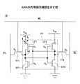
図1は、典型的なSRAM10の等価回路図を示す。 FIG. 1 shows an equivalent circuit diagram of a
図1を参照するに、前記SRAM10は第1のロードトランジスタLT1と第1のドライバトランジスタDT1を直列接続した第1のCMOSインバータI1と、第2のロードトランジスタLT2と第2のドライバトランジスタLD2を直列接続した第2のCMOSインバータI2とよりなるフリップフロップ回路FFを含み、前記第1のロードトランジスタLT1と第1のドライバトランジスタDT1を接続する接続ノードN1は、ワードラインWLにより制御される第1のトランスファトランジスタTF1を介して第1のビットラインBLに接続される。同様に、前記第2のロードトランジスタLT2と第1のドライバトランジスタDT2を接続する接続ノードN2は、ワードラインWLにより制御される第2のトランスファトランジスタTF2を介して第1のビットライン/BLに接続される。 Referring to FIG. 1, the SRAM 10 includes a first CMOS inverter I1 in which a first load transistor LT1 and a first driver transistor DT1 are connected in series, a second load transistor LT2 and a second driver transistor LD2 in series. A connection node N1 including a flip-flop circuit FF including a connected second CMOS inverter I2 and connecting the first load transistor LT1 and the first driver transistor DT1 is controlled by a word line WL. It is connected to the first bit line BL via the transfer transistor TF1. Similarly, the connection node N2 connecting the second load transistor LT2 and the first driver transistor DT2 is connected to the first bit line / BL via the second transfer transistor TF2 controlled by the word line WL. Is done.
かかる構成のSRAMでは、特にドライバトランジスタDT1,DT2を駆動するロードトランジスタLT1,LT2の電流駆動能力が、SRAMの高速動作において非常に重要である。
図2(A)は、このような等価回路に対応する本発明の関連技術によるSRAMレイアウトを示す。また図2(B)は図2(A)中、線A−A'に沿った断面図を示す。 FIG. 2A shows an SRAM layout according to the related art of the present invention corresponding to such an equivalent circuit. FIG. 2B is a cross-sectional view taken along line AA ′ in FIG.
図2(A),(B)を参照するに、シリコン基板11の表面にはn型ウェル11Nとp型ウェル11Pがイオン注入により形成されており、前記n型ウェル11N中には素子分離領域11Iによりn型素子領域11A1,11A2が、対称な関係で形成されている。また前記p型ウェル11P中には前記素子分離領域11Iにより、p型素子領11B,11Cが形成されている。2A and 2B, an n-
前記n型素子領域11A1,11A2には図1のpチャネルMOSトランジスタよりなるロードトランジスタLT1とLT2がそれぞれ形成され、前記ロードトランジスタLT1は、前記素子領域11A1を横断するp型ポリシリコンゲート電極G1を、前記ロートトランジスタLT2は、前記素子領域11A2を横断するp型ポリシリコンゲート電極G2を有する。In the n-
前記n型素子領域11A1のうち、前記ゲート電極G1の一方には電源コンタクトVDDが形成され、他方には、前記ポリシリコンゲート電極G2を前記素子領域11A1に接続するビアプラグV2が形成されている。A part of the n-
同様に前記n型素子領域11A2のうち、前記ゲート電極G2の一方には電源コンタクトVDDが形成され、他方には、前記ポリシリコンゲート電極G1を前記素子領域11A2に接続するビアプラグV4が形成されている。Similarly a part of the n-
さらに前記n型ウェル11Nの左側のp型ウェル11Pでは、前記素子分離領域11Iが前記p型素子領域11Bを画成しており、前記p型素子領域11Bのうち幅広部分には、n型ポリシリコンゲート電極G3を有するnチャネルMOSトランジスタが、前記ドライバトランジスタDT1として、また前記p型素子領域11Bのうち幅狭部分にはn型ポリシリコンゲート電極G4を有するnチャネルMOSトランジスタが、前記トランスファトランジスタTF1として形成されている。Further, in the p-
同様に前記n型ウェル11Nの右側のp型ウェル11Pでは、前記素子分離領域11Iが前記p型素子領域11Cを画成しており、前記p型素子領域11Cのうち幅広部分には、n型ポリシリコンゲート電極G5を有するnチャネルMOSトランジスタが、前記ドライバトランジスタDT2として、また前記p型素子領域11Cのうち幅狭部分にはn型ポリシリコンゲート電極G6を有するnチャネルMOSトランジスタが、前記トランスファトランジスタTF2として形成されている。Similarly, in the p-
前記素子領域11Bのうち、前記ゲート電極G3とG4の間にはビアコンタクトV1が形成され、前記ビアコンタクトV1は前記ビアコンタクトV2に、局所配線パターン(図示せず)により接続されている。同様に前記素子領域11Cのうち、前記ゲート電極G5とG6の間にはビアコンタクトV3が形成され、前記ビアコンタクトV3は前記ビアコンタクトV4に、局所配線パターン(図示せず)により接続されている。ここで前記ビアコンタクトV1およびV2は図1のノードN1を構成し、ビアコンタクトV3およびV4はノードN2を構成する。Part of the
さらに前記p型素子領域11B中、前記ゲート電極G3に対して前記ビアコンタクトV1の反対側には接地コンタクトVSSが形成され、また前記ゲート電極G4に対して前記ビアコンタクトV1の反対側には、ビットラインBLに接続されるビアコンタクトV5が形成されている。同様に、前記p型素子領域11C中、前記ゲート電極G5に対して前記ビアコンタクトV3の反対側には接地コンタクトVSSが形成され、また前記ゲート電極G6に対して前記ビアコンタクトV3の反対側には、ビットライン/BLに接続されるビアコンタクトV6が形成されている。Further in the p-
さらに図2のレイアウトでは、前記n型素子領域11A1を横切って、別のメモリセルのゲート電極G7が形成されている。In yet layout of Figure 2, across the n-
ところで、このような構成のSRAMの単ビット不良部のロードトランジスタについてその特性を解析したところ、図3に示す興味深い結果が得られた。 By the way, when the characteristics of the load transistor of the single bit defective portion of the SRAM having such a configuration were analyzed, an interesting result shown in FIG. 3 was obtained.
図3を参照するに、横軸はゲート電圧、縦軸はドレイン電流を示すが、符号2で示した実験では大きなドレイン電流が得られているのに対し、符号1で示した実験では、同じゲート電圧に対して得られるドレイン電流が減少しているのがわかる。 Referring to FIG. 3, the horizontal axis indicates the gate voltage, and the vertical axis indicates the drain current. In the experiment indicated by
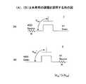
ここで前記符号1の実験は、図4(A)に示すようにロードトランジスタを構成するpチャネルMOSトランジスタのソース側に電源電圧VDDを印加しドレイン側を接地した場合を、また前記符号2の実験は図4(B)に示すように同じpチャネルMOSトランジスタのドレイン側に電源電圧VDDを印加しソース側を接地した場合を示しているが、図3の実験(1)でドレイン電流が小さく、実験(2)でドレイン電流が大きく事実は、図4(A),(B)に示すようにロードトランジスタのソース側に抵抗Rが入っていることを示している。すなわち、図4(A)の場合には電源電圧が印加されるソース側に抵抗Rが入っているために実効的にソース−ゲート間に印加される電圧VGSの大きさが減少してしまい、トランジスタが十分にオンしないのに対し、図4(B)の場合にはソース側にこのような抵抗が入っていないため、ソース−ゲート間電圧に抵抗Rによる電圧降下の効果が生じない。Here, the experiment of the
図1の等価回路図では、かかる抵抗Rは、図中破線で囲んだ部分に生じるものと考えられる。 In the equivalent circuit diagram of FIG. 1, the resistor R is considered to occur at a portion surrounded by a broken line in the drawing.
図5Aは、図2のSRAM中、破線で囲んだ部分の平面図を、図5Bは図5A中、線A−A'に沿った断面図を、さらに図5Cは図5A中、線B−B'に沿った断面図を示す。さらに図6は、図5B中、破線で囲んだ部分を拡大して示す図である。 5A is a plan view of a portion surrounded by a broken line in the SRAM of FIG. 2, FIG. 5B is a cross-sectional view taken along line AA ′ in FIG. 5A, and FIG. 5C is a line B-- in FIG. A cross-sectional view along B ′ is shown. Further, FIG. 6 is an enlarged view of a portion surrounded by a broken line in FIG. 5B.
図5Aを参照するに、前記シリコン基板11上に素子分離領域11Iにより画成されたn型素子領域11A1が形成され、これを横切ってゲート電極G1およびG7が延在し、その間に電源コンタクトVDDが形成されているのがわかる。またゲート電極G2と前記n型チャネル領域11A1を接続して、ビアコンタクトV2が形成されている。Referring to FIG. 5A, the silicon substrate 11 n-
図5Bの断面図に示すようにゲート電極G1,G2,G7は、それぞれn型にドープされたポリシリコンパターン13A,13B,13Cよりなり、各々両側に、典型的にはシリコン酸化膜よりなる側壁絶縁膜SWを担持している。As shown in the cross-sectional view of FIG. 5B, each of the gate electrodes G1 , G2 , and G7 is made of n-type doped
図5Bの断面では前記ポリシリコンパタ―ン13Aおよび13Cは、前記n型素子領域11A1上にゲート絶縁膜12Aおよび12Cを介して形成されているのに対し、前記ポリシリコンパターン13Bは前記素子分離絶縁膜11I上に形成されている。 In the cross section of FIG. 5B, the
前記素子領域11A1中、前記ゲート電極パターン13Aの一方の側にはp型ソースエクステンション拡散領域11aが、他方の側にはp型ドレインエクステンション拡散領域11bが形成され、同様に前記素子領域11A1中、前記ゲート電極パターン13Cの一方の側にはp型拡散ドレインエクステンション領域11cが、他方の側にはp型ソースエクステンション領域11dが形成される。In the
さらに前記n型素子領域11A1中、前記ゲート電極パターン13Aと13Cの間には、それぞれの側壁絶縁膜SWの外側に、p+型拡散領域11eが、前記ゲート電極G1およびG7を有するそれぞれのロードトランジスタのソース領域として形成されている。Further, in the n-
また前記n型素子領域11A1中、前記ゲート電極パターン13Aに対し前記ソース領域11eの反対側には、前記側壁絶縁膜SWと素子分離絶縁膜11Iとの間に、同様なp+型拡散領域よりなるドレイン領域11fが形成されている。Also in the n-
前記ポリシリコンゲート電極パターン13A〜13Cの表面にはシリサイド層14A〜14Cがそれぞれ形成されており、また前記ソース領域11eおよびドレイン領域11fの表面にはシリサイド層14eおよび14fが形成されている。 Silicide layers 14A to 14C are respectively formed on the surfaces of the polysilicon
さらに前記ポリシリコンゲート電極パターン13A〜13Cは、前記シリサイド層14A〜14Cおよび側壁絶縁膜SWを含めて、前記シリコン基板11上に形成された層間絶縁膜15により覆われ、前記ソース領域11eには前記ビアコンタクトVDDを構成するビアプラグ15Aが、前記シリサイド層14eを介してコンタクトする。また前記ドレイン領域11fには前記ビアコンタクトV2を構成するビアプラグ15Bが、前記シリサイド層14fを介してコンタクトする。その際、前記ポリシリコンゲート電極13B両側の側壁絶縁膜SWのうち前記ポリシリコンゲート電極パターン13Aの側の側壁絶縁膜は除去されており、このため前記ビアプラグ15Bは前記ポリシリコンゲート電極パターン14Bを前記ドレイン領域11fに電気的に接続する機能を果たす。Further, the polysilicon
さらに図5Cを参照するに、本発明が対象とするSRAMは非常に微細化されており、このため図5Aの断面B−B'で見た場合、前記ビアプラグ15Aの径が素子領域11A1の幅よりも大きくなっていることに注意すべきである。Further, referring to FIG. 5C, the SRAM targeted by the present invention is very miniaturized. For this reason, the diameter of the via
さて、前記ビアプラグ15A,15Bが正規の位置に形成されている場合には、図5A,図5B中に破線で示すようにビアプラグ15A,15Bはそれぞれ前記ソース領域11e,11fと、前記シリサイド層14e,14fを介して電気的にコンタクトし、その結果、ソース電流はビアプラグ15Aからソース領域11eへと前記シリサイド層11eを介して効率的に注入されるが、図5B中実線で示すようにビアプラグ15A,15Bがポリシリコンゲート電極パターン13Aの側に位置ずれを生じた場合には、図5B中、破線で示す小さな円で囲んで示すように、ビアプラグ15Aがp-型拡散領域11aと直接に接する状態が生じる恐れがある。When the via plugs 15A and 15B are formed at regular positions, the via plugs 15A and 15B have the
図6は、前記図5B中、前記ビアプラグ15A近傍を拡大して示す図である。6, in FIG 5B, is an enlarged view showing the
図6を参照するに、前記ビアプラグ15Aはその先端部がp-型拡散領域11a中に侵入しており、その結果、図6中、破線で囲んだ部分において前記p+型ソース領域11eからp型ソースエクステンション領域11a、およびポリシリコンゲート電極パターン13A直下のチャネル領域へのキャリアの経路が圧迫されているのがわかる。前記ビアプラグ15Aは一般にWなどの金属よりなるが、表面がTaやTiなどの金属、あるいはTiNなどの導電性化合物により覆われており、ビアプラグ15Aの界面から前記p-型ソース領域11a内部に延在する空乏層が、前記キャリア経路をさらに圧迫する。これが、前記図3および図4(A),(B)で説明したソース抵抗の原因と考えられる。 Referring to FIG. 6, the tip of the via
このようなソース抵抗がSRAMを構成するロードトランジスタの一方に、例えば前記図1中、破線で示した位置に発生すると、SRAMの動作が不安定になり、不良を引き起こす。 When such a source resistance occurs in one of the load transistors constituting the SRAM, for example, at the position indicated by the broken line in FIG. 1, the operation of the SRAM becomes unstable and causes a defect.
このようなビアプラグ15Aの位置ずれの問題は、前記側壁絶縁膜SWを、前記ビアプラグ15Aに対応したビアホールの形成に使われるドライエッチングに対して耐性を有する材料で形成する、いわゆる自己整合コンタクトの技術を使えば回避できると考えられるかも知れないが、図2のレイアウトを有するSRAMの場合には、図5Bに示すようにポリシリコンゲート電極G2の一方の側壁絶縁膜を除去する必要があるので、側壁絶縁膜SWを、エッチング耐性を有する材料により構成するのは困難である。The problem of such misalignment of the via
一の側面によれば本発明は、半導体基板と、前記半導体基板上、第1のノードで互いに直列接続された、互いに異なるチャネル導電型を有する第1および第2のMOSトランジスタを含む、第1のCMOSインバータと、前記半導体基板上、第2のノードで互いに直列接続された、互いに異なるチャネル導電型を有する第3および第4のMOSトランジスタを含む、前記第1のCMOSインバータとともにフリップフロップ回路を形成する、第2のCMOSインバータと、前記半導体基板上、第1のビット線と前記第1のノードとの間に設けられ、ワード線に接続された第1のゲート電極を有し、前記ワード線上の選択信号により駆動される第1のトランスファトランジスタと、前記半導体基板上、第2のビット線と前記第2のノードとの間に設けられ、前記ワード線に接続された第2のゲート電極を有し、前記ワード線上の選択信号により駆動される第2のトランスファトランジスタと、を有する半導体記憶装置であって、前記第1および第3のMOSトランジスタの各々は、前記半導体基板中に前記素子分離領域により画成された第1導電型の素子領域に形成されており、前記第1および第3のMOSトランジスタの各々は、前記半導体基板上にゲート絶縁膜を介して形成され、両側にゲート側壁絶縁膜を担持するポリシリコンゲート電極と、前記半導体基板中、前記ポリシリコンゲート電極の第1の側に、一端が前記ポリシリコンゲート電極直下の部分に侵入するように形成され、第2導電型を有するソース領域と、前記半導体基板中、前記第1の側とは反対の第2の側の表面部分に、一端が前記ポリシリコンゲート電極直下の部分に侵入するように形成された前記第2導電型を有するドレインエクステンション領域と、前記半導体基板中、前記第2の側のゲート側壁絶縁膜の外側に、前記ドレインエクステンション領域に重畳して、前記ドレインエクステンション領域よりも深く形成された第2導電型を有するドレイン領域と、前記素子領域の幅より大きい径を有し、前記ソース領域上に接続するビアプラグと、を有し、前記ソース領域は、前記ドレインエクステンション領域よりも深く形成されていることを特徴とする半導体記憶装置を提供する。The present invention According to one aspect, a semiconductor substrate, the semiconductor substrate, connected in series at a first nodeincludes first and second MOS transistors having different channel conductivity type to each other, the first of the CMOS inverter, the semiconductor substrate, connected in series at a second node,a third and fourth MOS transistors having different channel conductivity type to each other, the flip-flop circuit together with said first CMOS inverter A second CMOS inverter formed; and a first gate electrode provided on the semiconductor substrate between the first bit line and the first node and connected to a word line; A first transfer transistor driven by a selection signal on the line, and between the second bit line and the second node on the semiconductor substrate; Provided, having a second gate electrode connected to said word line, a semiconductor memory devicehaving a second transfer transistor being activated by a selection signal on said word line, said first and second Each of the three MOS transistors is formed in an element region of a first conductivity type defined by the element isolation region in the semiconductor substrate, and each of the first and third MOS transistors is formed in the semiconductor substrate. A polysilicon gate electrode formed on the substrate via a gate insulating film and carrying a gate sidewall insulating film on both sides, and one end of the polysilicon gate on the first side of the polysilicon gate electrode in the semiconductor substrate is formed so as to penetrate the portion immediately below theelectrode, the table opposite second side of the source region, in said semiconductor substrate, said first sidehaving a second conductivity type In part, a drain extension region having one endhaving formedthe second conductivity type so as to penetrate the part right underneath the polysilicon gate electrode, outside of the semiconductor substrate, a gate sidewall insulating film of the second side In addition,a drain regionhaving a second conductivity type, which is formed deeper than the drain extension region so as to overlap the drain extension region,has a diameter larger than the width of the element region, and is connected to the source region. a via plug, whereinthe source region is to provide a semiconductor memory device according to claimTei Rukoto formed deeper than said drain extension region.
他の側面によれば本発明は、半導体基板上、第1のノードで互いに直列接続され、互いに異なるチャネル導電型を有する第1および第2のMOSトランジスタを含む第1のCMOSインバータと、前記半導体基板上、第2のノードで互いに直列接続され、互いに異なるチャネル導電型を有する第3および第4のMOSトランジスタを含む、前記第1のCMOSインバータとともにフリップフロップ回路を形成する第2のCMOSインバータと、前記半導体基板上、第1のビット線と前記第1のノードとの間に設けられ、ワード線に接続された第1のゲート電極を有し、前記ワード線上の選択信号により駆動される第1のトランスファトランジスタと、前記半導体基板上、第2のビット線と前記第2のノードとの間に設けられ、前記ワード線に接続された第2のゲート電極を有し、前記ワード線上の選択信号により駆動される第2のトランスファトランジスタと、を有する半導体記憶装置の製造方法であって、前記半導体基板上、前記素子分離領域により画成された第1導電型の素子領域上にゲート絶縁膜を介して、前記第1のMOSトランジスタのゲート電極となる第1のポリシリコンパターンを、ポリシリコン膜のパターニングにより形成する工程と、前記素子領域中、前記第1のポリシリコンパターンの第1の側に第2導電型の不純物元素を導入し、前記素子領域のうち、前記第1のポリシリコンパターンの前記第1の側に第2導電型のソース領域を形成する工程と、前記素子領域中、前記第1のポリシリコンパターンの前記第1の側、および反対側の第2の側に、前記第2導電型の不純物元素を導入し、前記素子領域中、前記第1のポリシリコンパターンの前記第2の側の表面部分に、前記ソース領域よりも不純物濃度の低いドレインエクステンション領域を形成する工程と、前記第1のポリシリコンパターンのそれぞれの側壁面に側壁絶縁膜を形成する工程と、前記素子領域中に、前記第2導電型の不純物元素を前記1のポリシリコンパターンおよび前記側壁絶縁膜をマスクに導入し、前記第1のポリシリコンパターンの前記第1および第2の側の、前記側壁絶縁膜よりも外側の部分に前記第2導電型のドレイン領域を形成する工程と、前記半導体基板上及び前記第1のMOSトランジスタ上に層間絶縁膜を形成する工程と、前記層間絶縁膜に、前記素子領域の幅より大きい径を有し、前記ソース領域に接続するビアプラグを形成する工程と、を含むことを特徴とする半導体記憶装置の製造方法。According to another aspect, the present invention provides a first CMOS inverterincluding first and second MOS transistors connected in series at a first node on a semiconductor substrate and having different channel conductivity types, and the semiconductor A second CMOS inverter which forms a flip-flop circuit together with the first CMOS inverter, including third and fourth MOS transistors connected in series at a second node on the substrate and having different channel conductivity types; A first gate electrode provided on the semiconductor substrate between the first bit line and the first node and connected to the word line, and driven by a selection signal on the word line; Provided on the semiconductor substrate between the second bit line and the second node, and connected to the word line. A second gate electrode which is continued, the second transfer transistor driven by the word line selection signal, a method of manufacturing a semiconductor memory devicehaving a semiconductor substrate on said isolation region via a gate insulating film on the first conductive type element region which is defined by a first polysilicon pattern as a gate electrode of said first MOStransistor, and forming by patterning theport Rishirikon film In the element region, an impurity element of a second conductivity type is introduced into the first side of the first polysilicon pattern, and the element region has a first side of the first polysilicon pattern. and asfactories that form a source region of the second conductivity type, in the device region, said first side of said first polysilicon pattern, and on a second side oppositethe front Stories second electrically Introducing an impurity element of the mold, in the device region, on the surface part of the second side of said first polysilicon pattern, asengineering that form a low drain extension region impurity concentration than the source region and , Forming a sidewall insulating film on each sidewall surface of thefirst polysilicon pattern, and removing the second conductive type impurity element in the element region from the first polysilicon pattern and the sidewall insulating film. Introducing the drain region of the second conductivity type into a portion outside the side wall insulating film on the first and second sides of the first polysilicon pattern introduced into a mask; and thesemiconductor substrate Forming an interlayer insulating film on the upper MOS transistor and the first MOS transistor; and having a diameter larger than the width of the element region in the interlayer insulating film and connected to the source region. Forming a plug, and a method for manufacturing a semiconductor memory device.
半導体基板と、前記半導体基板上、第1のノードで互いに直列接続され、互いに異なるチャネル導電型を有する第1および第2のMOSトランジスタを含む第1のCMOSインバータと、前記半導体基板上、第2のノードで互いに直列接続され、互いに異なるチャネル導電型を有する第3および第4のMOSトランジスタを含み、前記第1のCMOSインバータとともにフリップフロップ回路を形成する第2のCMOSインバータと、前記半導体基板上、第1のビット線と前記第1のノードとの間に設けられ、ワード線に接続された第1のゲート電極を有し、前記ワード線上の選択信号により駆動される第1のトランスファトランジスタと、前記半導体基板上、第2のビット線と前記第2のノードとの間に設けられ、前記ワード線に接続された第2のゲート電極を有し、前記ワード線上の選択信号により駆動される第2のトランスファトランジスタと、を有する半導体記憶装置であって、前記第1のMOSトランジスタは、前記半導体基板上に素子分離領域により画成された帯状の第1の素子領域中に形成され、前記第1の素子領域を横断する第1のポリシリコンパターンを有するゲート電極を有し、前記第3のMOSトランジスタは、前記半導体基板上に前記素子分離領域により画成された帯状の第2の素子領域中に形成され、前記第2の素子領域を横断する第2のポリシリコンパターンを有するゲート電極を有し、前記第1のポリシリコンパターンは、前記第2の素子領域の第1の端部に、第1のビアプラグにより接続されており、前記第2のポリシリコンパターンは、前記第1の素子領域の第1の端部に、第2のビアプラグにより接続されており、前記第1の素子領域のうち、前記第1のポリシリコンパターンに対し前記第2のビアプラグと反対の側には、電源コンタクトを構成する第3のビアプラグがコンタクトしており、前記第2の素子領域のうち、前記第2のポリシリコンパターンに対し前記第1のビアプラグと反対の側には、電源コンタクトを構成する第4のビアプラグがコンタクトしており、前記第3のビアプラグは、前記第1の素子領域の幅よりも大きな径を有し、前記第4のビアプラグは、前記第2の素子領域の幅よりも大きな径を有し、前記第3のビアプラグは、前記第1の素子領域の中心線からずれて形成されており、前記第4のビアプラグは、前記第2の素子領域の中心線からずれて形成されており、前記第1の素子領域は、第1の縁と前記第1の縁と対向する第2の縁を有し、前記第1の素子領域は、前記第3のビアプラグと接続し、前記第1の縁に接し、前記第2の縁に接しない第1の部分と、前記第3のビアプラグと接続せず、前記第1の部分及び前記第2の縁に接する第2の部分を有し、前記第2の素子領域は、第3の縁と前記第3の縁と対向する第4の縁を有し、前記第2の素子領域は、前記第4のビアプラグと接続し、前記第3の縁に接し、前記第4の縁に接しない第3の部分と、前記第4のビアプラグと接続せず、前記第3の部分及び前記第4の縁に接する第4の部分を有することを特徴とする半導体記憶装置を提供する。A first CMOS inverterincluding first and second MOS transistors connected in series with each other at a first node and having different channel conductivity types on the semiconductor substrate; on the semiconductor substrate; A second CMOS inverterincluding third and fourth MOS transistors connected in series at different nodes and having different channel conductivity types to form a flip-flop circuit together with the first CMOS inverter; and on the semiconductor substrate A first transfer transistor provided between the first bit line and the first node and having a first gate electrode connected to the word line and driven by a selection signal on the word line; And provided on the semiconductor substrate between the second bit line and the second node and connected to the word line. A second gate electrode, a semiconductor memory devicehaving a second transfer transistor being activated by a selection signal on said word line, said first MOS transistor, the isolation on the semiconductor substrateA gate electrodehaving a first polysilicon pattern formed in the first element region in a band shape defined by the region and traversing the first element region; andA gate electrodehaving a second polysilicon pattern formed on a semiconductor substrate in a second element region in a band shape defined by the element isolation region and traversing the second element region; The first polysilicon pattern is connected to the first end of the second element region by a first via plug, and the second polysilicon pattern is connected to the first element region. The first end portion of the element region of the are connected by a second via-plug, said one of the first element region, said first side opposite to thesecond plug to the polysilicon pattern The third via plug constituting the power contact is in contact, and the power contact is arranged on the side of the second element region opposite to thefirst via plug with respect to the second polysilicon pattern. The third via plug has a diameter larger than the width of the first element region, and the fourth via plug has a diameter larger than the width of the second element region. The third via plug is formed so as to be shifted from the center line of the first element region, and the fourth via plug is shifted from the center line of the second element region. FormedThe first element region has a first edge and a second edge opposite to the first edge; the first element region is connected to the third via plug; and A first portion that contacts one edge and does not contact the second edge; and a second portion that does not connect to the third via plug and contacts the first portion and the second edge. The second element region has a third edge and a fourth edge opposite to the third edge, the second element area is connected to the fourth via plug, and A third portion that is in contact with the edge of the first electrode and not in contact with the fourth edge, and a fourth portion that is not connected with the fourth via plug and is in contact with the third portion and the fourth edge. A featured semiconductor memory device is provided.
本発明によれば、SRAMを構成するロードトランジスタにおいて電源コンタクトに位置ずれが生じても、ソース抵抗の増大が回避され、不良の発生を回避することができる。 According to the present invention, even when a power supply contact is misaligned in a load transistor constituting an SRAM, an increase in source resistance can be avoided and occurrence of a defect can be avoided.
[第1の実施形態]
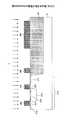
図7(A)は、本発明の第1の実施形態よるSRAM20のレイアウトを示す。また図7(B)は図7(A)中、線A−A'に沿った断面図を示す。[First embodiment]
FIG. 7A shows a layout of the
図7(A),(B)を参照するに、前記SRAM20はシリコン基板21上に形成され、図1に示したのと同じ等価回路を構成する。 Referring to FIGS. 7A and 7B, the
より具体的には、前記シリコン基板21の表面にはn型ウェル21Nとp型ウェル21Pがイオン注入により形成されており、前記n型ウェル21N中には素子分離領域21Iによりn型素子領域21A1,21A2が、点対称な関係で形成されている。また前記p型ウェル21P中には前記素子分離領域21Iにより、p型素子領域21B,21Cが形成されている。More specifically, an n-type well 21N and a p-
前記n型素子領域21A1,21A2には図1のpチャネルMOSトランジスタよりなるロードトランジスタLT1とLT2がそれぞれ形成され、前記ロードトランジスタLT1は、前記素子領域21A1を横断するp型ポリシリコンゲート電極G1を、前記ロートトランジスタLT2は、前記素子領域21A2を横断するp型ポリシリコンゲート電極G2を有する。The n-
前記n型素子領域21A1のうち、前記ゲート電極G1の一方には電源コンタクトVDDが形成され、他方には、前記ポリシリコンゲート電極G2を前記素子領域21A1に接続するビアプラグV2が形成されている。In the n-
同様に前記n型素子領域21A2のうち、前記ゲート電極G2の一方には電源コンタクトVDDが形成され、他方には、前記ポリシリコンゲート電極G1を前記素子領域21A2に接続するビアプラグV4が形成されている。Similarly a part of the n-
さらに前記n型ウェル21Nの左側のp型ウェル21Pでは、前記素子分離領域21Iが前記p型素子領域21Bを画成しており、前記p型素子領域21Bのうち幅広部分には、n型ポリシリコンゲート電極G3を有するnチャネルMOSトランジスタが、前記ドライバトランジスタDT1として、また前記p型素子領域21Bのうち幅狭部分にはn型ポリシリコンゲート電極G4を有するnチャネルMOSトランジスタが、前記トランスファトランジスタTF1として形成されている。Further, in the p-
同様に前記n型ウェル21Nの右側のp型ウェル21Pでは、前記素子分離領域21Iがp型素子領域21Cを画成しており、前記p型素子領域21Cのうち幅広部分には、n型ポリシリコンゲート電極G5を有するnチャネルMOSトランジスタが、前記ドライバトランジスタDT2として、また前記p型素子領域21Cのうち幅狭部分にはn型ポリシリコンゲート電極G6を有するnチャネルMOSトランジスタが、前記トランスファトランジスタTF2として形成されている。Similarly, in the p-
前記素子領域21Bのうち、前記ゲート電極G3とG4の間にはビアコンタクトV1が形成され、前記ビアコンタクトV1は前記ビアコンタクトV2に、局所配線パターン(図示せず)により接続されている。同様に前記素子領域21Cのうち、前記ゲート電極G5とG6の間にはビアコンタクトV3が形成され、前記ビアコンタクトV3は前記ビアコンタクトV4に、局所配線パターン(図示せず)により接続されている。ここで前記ビアコンタクトV1およびV2は図1のノードN1を構成し、ビアコンタクトV3およびV4はノードN2を構成する。A via contact V1 is formed between the gate electrodes G3 and G4 in the
さらに前記p型素子領域21B中、前記ゲート電極G3に対して前記ビアコンタクトV2の反対側には接地コンタクトVSSが形成され、また前記ゲート電極G4に対して前記ビアコンタクトV1の反対側には、ビットラインBLに接続されるビアコンタクトV5が形成されている。同様に前記p型素子領域21C中、前記ゲート電極G5に対して前記ビアコンタクトV3の反対側には接地コンタクトVSSが形成され、また前記ゲート電極G6に対して前記ビアコンタクトV3の反対側には、ビットライン/BLに接続されるビアコンタクトV6が形成されている。Further in the p-
さらに図7(A)のレイアウトでは、前記n型素子領域21A1を横切って、別のメモリセルのゲート電極G7が形成されており、さらに同じシリコン基板21上の別の部分において、素子分離構造21I上にポリシリコンパターンよりなる抵抗素子Rが形成されている。前記抵抗素子Rには、ビアコンタクトVR1,VR2が形成されているのがわかる。Further, in the layout of FIG. 7A, the gate electrode G7 of another memory cell is formed across the n-
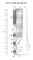
図8は図7中、線B−B'に沿った断面図を示す。 FIG. 8 is a cross-sectional view taken along line BB ′ in FIG.
図8を参照するに、ゲート電極G1,G2,G7は、それぞれn型にドープされたポリシリコンパターン23A,23B,23Cよりなり、各々両側に、典型的にはシリコン酸化膜よりなる側壁絶縁膜SWを担持している。Referring to FIG. 8, gate electrodes G1 , G2 , and G7 are made of n-type doped
図8の断面では前記ポリシリコンパタ―ン23Aおよび23Cは、前記n型素子領域21A1上にゲート絶縁膜22Aおよび22Cを介して形成されているのに対し、前記ポリシリコンパターン23Bは前記素子分離絶縁膜21I上に形成されている。Wherein in the cross section of FIG. 8 polysilicon pattern -
さて、本実施形態によるSRAM20では、前記素子領域21A1中、前記ゲート電極パターン23Aの一方の側にはp+型拡散領域21aがソース領域として形成され、他方の側にはp型拡散領域21bが、ドレインエクステンション領域として形成される。同様に前記素子領域21A1中、前記ゲート電極パターン13Cの一方の側にはp型拡散領域21cがドレインエクステンション領域として形成され、他方の側には前記p+型拡散領域21aが、ソース領域として、共通に形成される。In the
さらに前記n型素子領域21A1中、前記ゲート電極パターン23Aに対し前記ソース領域21aの反対側には、前記側壁絶縁膜SWと素子分離絶縁膜21Iとの間にp+型拡散領域よりなるドレイン領域21dが形成されている。Further in the n-
前記ポリシリコンゲート電極パターン23A〜23Cの表面にはシリサイド層24A〜24Cがそれぞれ形成されており、また前記ソース領域21aおよびドレイン領域21dの表面にはシリサイド層24aおよび24dが形成されている。 Silicide layers 24A to 24C are respectively formed on the surfaces of the polysilicon
前記シリコン基板21上には、前記ポリシリコンゲート電極パターン23A〜23Cを、前記シリサイド層24A〜24Cおよび側壁絶縁膜SWをも含めて覆うように層間絶縁膜25が形成されており、前記層間絶縁膜25中には前記ソース領域21aに対応して、前記ビアコンタクトVDDを構成するビアプラグ25Aが、前記シリサイド層24aを介してコンタクトするように形成されている。同様に、前記層間絶縁膜25には、前記ドレイン領域21dに対応して、前記ビアコンタクトV2を構成するビアプラグ25Bが、前記シリサイド層24dを介してコンタクトするように形成されている。前記ポリシリコンゲート電極23B両側の側壁絶縁膜SWのうち前記ポリシリコンゲート電極パターン23Aの側の側壁絶縁膜は除去されており、このため前記ビアプラグ25Bは前記ポリシリコンゲート電極パターン23Bを前記ドレイン領域21dに電気的に接続する機能を果たす。An interlayer insulating
さらに図8のSRAM20では、同じシリコン基板21上、他の部分に形成された素子分離領域21I上に、ポリシリコンパターン23Dが、前記ポリシリコン抵抗素子Rとして形成されており、前記層間絶縁膜25中には前記ポリシリコンパターン23Dとコンタクトするビアプラグ25E,25Fが、それぞれシリサイド層24eおよび24fを介して形成されている。なお前記ポリシリコンパターン23Dは前記ポリシリコンゲートパタ―ン23A〜23Cと同時に形成され、同様に側壁絶縁膜SWを形成されている。また図示の例では、前記ポリシリコンパターン23D上には、前記シリサイド層24eおよび24fを形成する際にマスクとなる誘電体パターン25dが残っている。 Further, in the
本実施形態では、前記抵抗素子Rを構成するポリシリコンパターン23Dを、前記ポリシリコンゲート電極パターン23A〜23Cと同時に、同一のポリシリコン膜のパターニングにより形成しており、このため前記ポリシリコンパターン23Dは、前記ポリシリコンゲート電極パターン23A〜23Dの各々と同一の膜厚、従って高さを有し、また同一の不純物元素により、同一の濃度にドープされている。 In the present embodiment, the
以下、図8のSRAM20の製造工程を、図9(A)〜13(G)を参照しながら説明する。 Hereinafter, the manufacturing process of the
図9Aを参照するに、シリコン基板21上にはポリシリコンパターン23A〜23Dがポリシリコン膜(図示せず)のパターニングにより、前記ポリシリコンパターン23Aおよび23Cは素子領域21A1中にそれぞれゲート絶縁膜22Aおよび22Cを介して、また前記ポリシリコンパターン23Bおよび23Dは前記素子領域21A1を画成する素子分離絶縁膜21I上に形成される。なお以下の説明では、前記抵抗素子Rとなるポリシリコンパターン23Dは、前記ポリシリコンパターン23Bを担持する素子分離絶縁膜21I上に担持されている構成について説明するが、本実施形態はかかる特定の構成に限定されるものではない。Referring to FIG. 9A, by patterning the
次いで図9Bの工程において、前記素子領域21A1が、前記ポリシリコンパターン23Aとポリシリコンパターン23Bの間の部分を除いて、レジストパターンRにより覆われ、前記素子領域21A1のうち、前記レジストパターンRにより覆われていない部分にB+が、8keVの加速電圧下、4.0×1015cm-2のドーズ量でイオン注入される。その結果、前記素子領域21A1中、前記ポリシリコンパターン23Aと23Cの間に、前記p+型拡散領域21aが形成される。また同時に前記図9Bの工程では、前記ポリシリコンパターン21A〜21Cおよび前記素子分離絶縁膜21I上のポリシリコンパターン23Dが、Bにより、p+型にドープされる。Then, in the step of Figure 9B, the
次いで図9Cの工程において前記レジストパターンRは除去され、前記素子領域21A1に、前記ポリシリコンパターン23A,23CをマスクにB+がイオン注入され、前記素子領域21A1のうち、前記ポリシリコンパターン23Aおよび23Cの、それぞれ前記ソース領域21aとは反対の側に、p型ドレインエクステンション領域21b,21cが形成される。また同時に、前記ソース領域21aの表面部分に同様な注入領域21b'が、重畳して形成される。Then the above resist pattern R in the step of FIG. 9C is removed, in the device region 21A1, the
さらに図7Cのイオン注入工程では、前記ポリシリコンパターン23A〜23Cおよび23Dにも、同じBのイオン注入が、同じ条件でなされる。 Further, in the ion implantation step of FIG. 7C, the same B ions are implanted into the
次に図9Dの工程において前記図9Dの構造上に絶縁膜(図示せず)をCVD法により堆積し、これを基板面に略垂直方向に作用する異方性エッチングによりエッチバックすることにより、前記ポリシリコンパターン23A〜23Dのそれぞれの側壁面に側壁絶縁膜SWが形成され、次に図9Eの工程において、前記素子領域21A1にB+を、前記ポリシリコンパターン21Aおよび23Cおよびそれぞれの側壁絶縁膜SWをマスクにイオン注入することにより、前記p+型ドレイン領域21dが、前記ポリシリコンパターン23Aとポリシリコンパターン23Bを担持する素子分離絶縁膜21Iの間において前記ポリシリコンパターン23Aの側壁絶縁膜SWの外側の部分に形成される。また前記p+型ソース領域21aの内部にも、同様なBのイオン注入がなされ、前記p+型ソース領域21aに重畳して、p+型注入領域21d'が形成される。Next, in the step of FIG. 9D, an insulating film (not shown) is deposited on the structure of FIG. 9D by the CVD method, and this is etched back by anisotropic etching acting in a direction substantially perpendicular to the substrate surface. the sidewall insulation films SW to the respective sidewall surfaces of the
また前記図9Eの工程では、前記ポリシリコンパターン23A〜23DにもBのイオン注入が同じ条件でなされる。 In the step of FIG. 9E, B ions are also implanted into the
次に図9Fの工程において前記図9Eの構造の露出シリコン面に、サリサイド法によりシリサイド層が形成され、その結果、前記ポリシリコンパターン23A〜23C上にはシリサイド層24A〜24Cが、またソース領域21a、ドレイン領域21d上にはシリサイド層24a,24dが、それぞれ形成される。また抵抗素子Rとなるポリシリコンパターン23Dでは、誘電体パターン25dにより二つのシリサイド形成領域が、互いに離間して画成され、かかるシリサイド形成領域にはシリサイド層24eおよび24fが、それぞれ形成される。 Next, in the step of FIG. 9F, a silicide layer is formed on the exposed silicon surface of the structure of FIG. 9E by the salicide method. As a result,
次に図9Gの工程において、前記ポリシリコンパターン23Bの一方の側壁絶縁膜SWが除去され、さらに図9Hの工程において前記図9Gの構造上に層間絶縁膜25が、前記ポリシリコンパターン23A〜23Dを、それぞれの側壁絶縁膜SWおよびシリサイド層24A〜23C、24eおよび24fを覆うように形成される。 Next, in the process of FIG. 9G, one sidewall insulating film SW of the
さらに図9Hの工程では前記層間絶縁膜25中に前記シリサイド層24a,24dを露出するようにビアホールが形成され、かかるビアホールをそれぞれビアプラグ25Aおよび25Bで充填することにより、先に図1で説明した等価回路図に対応したSRAM20が得られる。 Further, in the step of FIG. 9H, via holes are formed in the
また図9Hの工程では同時に前記層間絶縁膜25中に前記ポリシリコンパターン23Dのシリサイド層24e,24fを露出するビアホールが形成され、かかるビアホールをビアプラグ25Dおよび25Eで充填することにより、前記ポリシリコンパターン23Dよりなる抵抗素子Rが同時に形成される。 9H, via holes are formed in the
図9Hは、前記ビアプラグ25A,25Bに位置ずれが無い場合を示しているが、図9Iに示すようにビアプラグ25A,25Bが、それぞれポリシリコンパターン23A,23B側にずれた場合でも、前記ビアプラグ25Aは高濃度拡散領域21aにコンタクトするため、前記ポリシリコンパターン23Aをゲート電極とするロードトランジスタにおいてソース抵抗の増大が生じることはなく、先に図3で説明したトランジスタ特性の変化の問題が生じることはない。 FIG. 9H shows a case where there is no displacement in the via plugs 25A and 25B. However, even when the via plugs 25A and 25B are displaced toward the
また本実施形態では、かかる高濃度拡散領域21aの形成をポリシリコン抵抗素子の形成と同時に行っているため、製造工程が増加したり製造費用が増大したりする問題が生じることはない。
[第2の実施形態]
ところで、図5Bで説明したような、ピアプラグ15Aの位置ずれに起因するロードトランジスタの特性変化の問題は、このように微細化されたSRAMでは図5Cで説明したように素子領域11A1の幅がビアプラグの径よりも縮小されていて、位置合わせに余裕のないところから発生しているものであり、従って、例えば図10に示すように素子領域11A1あるいは11A2の幅を、前記ビアコンタクトVDDの周辺で拡張することにより、上記の課題は解決できるとも考えられるであろう。ただし図10は前記図2のレイアウトのうち、素子領域11A1および11A2を含むn型ウェル部分を抜き出して示す図である。In the present embodiment, since the formation of the high-
[Second Embodiment]
Incidentally, as described in FIG. 5B, a problem of characteristic change of the load transistor caused by the positional deviation of
しかし、かかる構成は、図10に示すようにn型素子領域11A1が隣接するp型ウェルに近接し、特にコンタクトVDDには電源電圧が印加されることを勘案すると、耐圧が劣化し、SRAMが誤動作する恐れがあるため、採用できない。However, in this configuration, the n-
これに対し図11は、本発明の第2の実施形態によるSRAMのレイアウトを示す図である。ただし図11中、先に説明した部分に対応する部分には同一の参照符号を付し、説明を省略する。 On the other hand, FIG. 11 is a diagram showing the layout of the SRAM according to the second embodiment of the present invention. However, in FIG. 11, the same reference numerals are assigned to the portions corresponding to the portions described above, and the description thereof is omitted.
図11を参照するに、本実施形態では、前記図10のレイアウトのようビアコンタクトVDDに対応して素子領域11A1,11A2の幅を増大させることはせず、ビアコンタクトVDDの一を一方にずらしている。Referring to FIG. 11, in this embodiment, FIG. 10 not is to increase the width of the
かかる構成では、仮りに前記ビアコンタクトVDDの位置がずれてゲート電極G1あるいはG2に近接し、ビアコンタクトVDDからロードトランジスタのチャネルに流れるキャリア流が図11中に×で示すようにブロックされても、キャリアはブロックされていない迂回路を通って流れることができ、ソース抵抗の増大によるトランジスタ特性の劣化の問題を回避することができる。またn型素子領域11A1が隣接のp型ウェルに近接することがなく、耐圧低下の問題も生じない。なお図11中、白で示した素子領域11A1,11A2の露出部分は、実際にはシリサイド膜により覆われている。In such a configuration, the position of the via contact VDD is shifted so as to be close to the gate electrode G1 or G2 , and the carrier flow flowing from the via contact VDD to the channel of the load transistor is indicated by x in FIG. Even if blocked, the carrier can flow through an unblocked detour, and the problem of deterioration of transistor characteristics due to an increase in source resistance can be avoided. In addition, the n-
図12は、前記図11の素子領域11A1の平面図を示す。FIG. 12 is a plan view of the
図12を参照するに、前記素子領域11A1を横切って、前記ゲート電極G7に対応するポリシリコンパターン13Cと、前記ゲート電極G1に対応するポリシリコンパターン13Aと、前記ゲート電極G2に対応するポリシリコンパターン13Bとが、それぞれ側壁絶縁膜SWを担持して形成されており、前記ポリシリコンパターン13Aと13Cの間には、相対向する側壁絶縁膜SWの間に前記ビアコンタクトVDDを構成するビアプラグ15Aが形成されている。また前記ポリシリコンパターン13Bのうち、前記ポリシリコンパターン14Aに面する側では側壁絶縁膜SWが局所的に除去され、前記ビアコンタクトV2を構成するビアプラグ15Bが、前記ポリシリコンパターン13Bを前記素子領域11A1に接続している。Referring to FIG. 12, across the
図12においても、前記素子領域11A1のうち、白で示す露出部分は、CoSi2やNiSiなどのシリサイド膜により覆われている。Also in FIG. 12, the exposed portion shown in white in the
図13Aは、図12中、ビアコンタクトVDD、すなわちコンタクトプラグ15A近傍を抜き取って示した平面図、図13Bは、前記図13A中、線bx−bx1'に沿った断面図、図13Cは、前記図13A中、線bx2−bx2'に沿った断面図、図13Dは、前記図13A中、線by−by'に沿った断面図を示す。 13A is a plan view of the via contact VDD, that is, the contact plug 15A and its vicinity shown in FIG. 12, FIG. 13B is a sectional view taken along line bx-bx1 ′ in FIG. 13A, and FIG. 13A shows a cross-sectional view along line bx2-bx2 ′, and FIG. 13D shows a cross-sectional view along line by-by ′ in FIG. 13A.
図13A〜13Cを参照するに、前記線bx2−bx2'に沿った断面図では、前記図5Bの場合と同様な構造が生じており、ポリシリコンゲート電極13Aを有するロードトランジスタのチャネル領域を通過したキャリアは、図13C中に×印で示したようにソース領域11a中の経路がビアプラグ15Aにより圧迫されてソース抵抗が増大するのに対し、線bx−bx'に沿った断面では、ビアプラグ15Aが断面から外れており、キャリアは前記ソース領域11eからゲート電極パターン14C直下のチャネル領域へ、効率的に注入される。 13A to 13C, in the cross-sectional view along the line bx2-bx2 ′, a structure similar to that in the case of FIG. 5B occurs, and passes through the channel region of the load transistor having the
本実施形態においても、前記図13Dの断面に示すように、ビアプラグ15Aの径W1は素子領域11A1の幅W2よりも大きく(W1>W2)、例えば前記ビアプラグ15Aはその底部において100nm程度の径を有するのに対し、前記素子領域11A1は70nm程度の幅しか有さない。このような場合でも、ビアプラグ15Aの中心線c2を素子領域11A1の中心線c1に対して25nmずらすことにより(図12においてδ=25nm)、かかるビアプラグ15Aを迂回するキャリア経路として約10nmの幅を確保することができる。In this embodiment, as shown in the cross-section of FIG. 13D, the diameter W1 of the via-
本実施形態においても、図11,12の構成において前記素子領域11A1,11A2のうち、前記ビアプコンタクトVDDおよびV2を構成するビアプラグ15A,15B、およびゲート電極G1,G2を構成するポリシリコンパターン13A〜13Cおよびその側壁絶縁膜SWで覆われていない部分は、シリサイド膜により覆われている。In this embodiment, part of the
なお本実施形態では、前記ビアコンタクトVDDを、図11に示すようにn型ウェル11Nとp型ウェル11Pとのウェル境界WBの側にずらしていたが、逆にウェル境界WBから遠ざかるようにずらすことも可能である。
[第3の実施形態]
図14は、本発明の第3の実施形態によるSRAMのレイアウトを示す図である。ただし図14中、先に説明した部分に対応する部分には同一の参照符号を付し、説明を省略する。In the present embodiment, the via contact VDD is shifted toward the well boundary WB between the n-
[Third Embodiment]
FIG. 14 is a diagram showing the layout of the SRAM according to the third embodiment of the present invention. However, in FIG. 14, the same reference numerals are assigned to the portions corresponding to the portions described above, and the description thereof is omitted.
図14を参照するに、本実施形態では、前記図11のレイアウトと同様に、ビアコンタクトVDDの一を一方にずらすと共に、さらに素子領域11A1の幅を、前記ビアコンタクトVDDの形成箇所において隣接するp型ウェルの方向とは反対方向に拡張する。Referring to FIG. 14, in the present embodiment, as in the layout of FIG. 11, one of the via contacts VDD is shifted to one side, and the width of the
かかる構成では、仮りに前記ビアコンタクトVDDの位置がずれてゲート電極G1あるいはG2に近接し、ビアコンタクトVDDからロードトランジスタのチャネルに流れるキャリア流が図11中に×で示すようにブロックされても、キャリアはブロックされていない迂回路を通って流れることができ、ソース抵抗の増大によるトランジスタ特性の劣化の問題を回避することができる。またn型素子領域11A1が隣接のp型ウェルに近接することがなく、耐圧低下の問題も生じない。その際、前記素子領域11A1の幅が、図14中に一点鎖線で示すウェル境界WBの反対方向に拡大されているため、耐圧劣化の問題が生じることもない。In such a configuration, the position of the via contact VDD is shifted so as to be close to the gate electrode G1 or G2 , and the carrier flow flowing from the via contact VDD to the channel of the load transistor is indicated by x in FIG. Even if blocked, the carrier can flow through an unblocked detour, and the problem of deterioration of transistor characteristics due to an increase in source resistance can be avoided. In addition, the n-
本実施形態においても、ビアプラグ15Aの径W1は、前記図13Dの断面と同様で、素子領域11A1の幅W2よりも大きいが(W1>W2)、前記素子領域11A1の幅を40nm程度拡張し、ビアプラグ15Aの中心線c2を素子領域11A1の中心線c1に対して25nmずらすことにより、かかるビアプラグ15Aを迂回するキャリア経路として約30nmの幅を確保することができる。Also in this embodiment, the diameter W1 of the via
本実施形態においても、図14の構成において前記素子領域11A1,11A2のうち、前記ビアプコンタクトVDDおよびV2を構成するビアプラグ15A,15B、およびゲート電極G1,G2を構成するポリシリコンパターン13A〜13C、さらにその側壁絶縁膜SWで覆われていない部分は、シリサイド膜により覆われている。Also in this embodiment, via
このように、本発明の第2および第3の実施形態では、前記ビアコンタクトVDDの周囲にキャリアの迂回路となる領域を確保することで、コンタクトの位置ずれが生じた場合でもソース抵抗が増大するのを回避しているが、かかる迂回路は、10〜30nm程度の幅があれば十分である。As described above, in the second and third embodiments of the present invention, by securing a region serving as a carrier detour around the via contact VDD , the source resistance is reduced even when the contact is misaligned. Although an increase is avoided, it is sufficient that such a detour has a width of about 10 to 30 nm.
なお、以上の各実施形態において、p型とn型の導電型を反転させても本発明が成立することは明らかである。 In each of the above embodiments, it is clear that the present invention can be realized even if the p-type and n-type conductivity types are reversed.
本発明では、前記シリサイド層は特に限定されないが、例えばCoSi2やNiSiなどを使うことができる。In the present invention, the silicide layer is not particularly limited, but for example, CoSi2 or NiSi can be used.
以上、本発明を好ましい実施形態について説明したが、本発明はかかる特定の実施形態に限定されるものではなく、特許請求の範囲に記載した要旨内において様々な変形・変更が可能である。 As mentioned above, although this invention was described about preferable embodiment, this invention is not limited to this specific embodiment, A various deformation | transformation and change are possible within the summary described in the claim.
(付記1)
半導体基板と、
前記半導体基板上、第1のノードで互いに直列接続された、互いに異なるチャネル導電型を有する第1および第2のMOSトランジスタよりなる、第1のCMOSインバータと、
前記半導体基板上、第2のノードで互いに直列接続された、互いに異なるチャネル導電型を有する第3および第4のMOSトランジスタよりなり、前記第1のCMOSインバータとともにフリップフロップ回路を形成する、第2のCMOSインバータと、
前記半導体基板上、第1のビット線と前記第1のノードとの間に設けられ、ワード線に接続された第1のゲート電極を有し、前記ワード線上の選択信号により駆動される第1のトランスファトランジスタと、
前記半導体基板上、第2のビット線と前記第2のノードとの間に設けられ、前記ワード線に接続された第2のゲート電極を有し、前記ワード線上の選択信号により駆動される第2のトランスファトランジスタと、
前記半導体基板上の素子分離領域上に形成されたポリシリコン抵抗素子と、
よりなる半導体記憶装置であって、
前記第1および第3のMOSトランジスタの各々は、前記半導体基板中に前記素子分離領域により画成された第1導電型の素子領域に形成されており、
前記第1および第3のMOSトランジスタの各々は、
前記半導体基板上にゲート絶縁膜を介して形成され、両側にゲート側壁絶縁膜を担持するポリシリコンゲート電極と、
前記半導体基板中、前記ポリシリコンゲート電極の第1の側に、一端が前記ポリシリコンゲート電極直下の部分に侵入するように形成された第2導電型ソース領域と、
前記半導体基板中、前記第1の側とは反対の第2の側の表面部分に、一端が前記ポリシリコンゲート電極直下の部分に侵入するように形成された第2導電型ドレインエクステンション領域と、
前記半導体基板中、前記第2の側のゲート側壁絶縁膜の外側に、前記ドレインエクステンション領域に重畳して、前記ドレインエクステンション領域よりも深く形成された第2導電型ドレイン領域と、
よりなり、
前記ソース領域は、前記ドレインエクステンション領域よりも深く形成されており、
前記ポリシリコンゲート電極は、前記ポリシリコン抵抗素子と同一の膜厚を有し、
前記ソース領域と前記ポリシリコン抵抗素子とは、同じドーパント元素により、ドーピングされていることを特徴とする半導体記憶装置。(Appendix 1)
A semiconductor substrate;
A first CMOS inverter comprising first and second MOS transistors having different channel conductivity types connected in series to each other at a first node on the semiconductor substrate;
A second and second MOS transistors having different channel conductivity types connected in series at a second node on the semiconductor substrate, and forming a flip-flop circuit together with the first CMOS inverter; CMOS inverter,
A first gate electrode is provided between the first bit line and the first node on the semiconductor substrate, and has a first gate electrode connected to the word line, and is driven by a selection signal on the word line. Transfer transistors,
A second gate electrode is provided between the second bit line and the second node on the semiconductor substrate and connected to the word line, and is driven by a selection signal on the word line. Two transfer transistors;
A polysilicon resistance element formed on an element isolation region on the semiconductor substrate;
A semiconductor memory device comprising:
Each of the first and third MOS transistors is formed in an element region of a first conductivity type defined by the element isolation region in the semiconductor substrate,
Each of the first and third MOS transistors includes:
A polysilicon gate electrode formed on the semiconductor substrate via a gate insulating film and carrying a gate sidewall insulating film on both sides;
A second conductivity type source region formed on the first side of the polysilicon gate electrode in the semiconductor substrate so that one end of the semiconductor substrate enters a portion directly under the polysilicon gate electrode;
A second conductivity type drain extension region formed on the surface portion of the second side opposite to the first side in the semiconductor substrate so that one end penetrates into a portion directly under the polysilicon gate electrode;
A second conductivity type drain region formed deeper than the drain extension region, overlapping the drain extension region outside the gate sidewall insulating film on the second side in the semiconductor substrate;
More
The source region is formed deeper than the drain extension region,
The polysilicon gate electrode has the same film thickness as the polysilicon resistance element,
The semiconductor memory device, wherein the source region and the polysilicon resistance element are doped with the same dopant element.
(付記2)
前記ソース領域は、前記ドレインエクステンション領域よりも高い不純物濃度を有することを特徴とする付記1記載の半導体記憶装置。(Appendix 2)
The semiconductor memory device according to
(付記3)
前記ソース領域は、前記ドレインエクステンション領域およびドレイン領域のいずれよりも深く形成されていることを特徴とする付記1または2記載の半導体記憶装置。(Appendix 3)
The semiconductor memory device according to
(付記4)
前記素子分離領域上には、前記ドレイン領域に近接して、前記第1および第3のMOSトランジスタのうち、他方のMOSトランジスタのゲート電極を構成するポリシリコンパターンが延在し、前記ソース領域には第1のシリサイド層を介して第1のビアプラグがコンタクトし、前記ドレイン領域には、第2のシリサイド層を介して第2のビアプラグがコンタクトし、前記ポリシリコン抵抗素子の第1の領域および第2の領域には、それぞれ第3および第4のシリサイド層を介して第3および第4のビアプラグがコンタクトし、前記第2のビアプラグは、同時に前記ポリシリコンパターンの上面に第5のシリサイド層を介してコンタクトし、また前記ポリシリコンパターンの、前記ポリシリコンゲート電極に面する側の側壁面にコンタクトすることを特徴とする付記1〜3のうち、いずれか一項記載の半導体記憶装置。(Appendix 4)
A polysilicon pattern constituting the gate electrode of the other MOS transistor of the first and third MOS transistors extends on the element isolation region in the vicinity of the drain region, and extends to the source region. The first via plug contacts through the first silicide layer, and the second via plug contacts through the second silicide layer to the drain region, and the first region of the polysilicon resistance element and The second region is in contact with the third and fourth via plugs via the third and fourth silicide layers, respectively, and the second via plugs are simultaneously formed on the upper surface of the polysilicon pattern with the fifth silicide layer. And contact the side wall surface of the polysilicon pattern facing the polysilicon gate electrode. Of
(付記5)
半導体基板上、第1のノードで互いに直列接続され、互いに異なるチャネル導電型を有する第1および第2のMOSトランジスタよりなる第1のCMOSインバータと、
前記半導体基板上、第2のノードで互いに直列接続され、互いに異なるチャネル導電型を有する第3および第4のMOSトランジスタよりなり、前記第1のCMOSインバータとともにフリップフロップ回路を形成する第2のCMOSインバータと、
前記半導体基板上、第1のビット線と前記第1のノードとの間に設けられ、ワード線に接続された第1のゲート電極を有し、前記ワード線上の選択信号により駆動される第1のトランスファトランジスタと、
前記半導体基板上、第2のビット線と前記第2のノードとの間に設けられ、前記ワード線に接続された第2のゲート電極を有し、前記ワード線上の選択信号により駆動される第2のトランスファトランジスタと、
前記半導体基板上の素子分離領域上に形成されたポリシリコン抵抗素子と、
よりなる半導体記憶装置の製造方法であって、
前記半導体基板上、前記素子分離領域により画成された第1導電型の素子領域上にゲート絶縁膜を介して、前記第1のMOSトランジスタのゲート電極となる第1のポリシリコンパターンを、前記素子分離領域上のポリシリコン抵抗素子を構成する第2のポリシリコンパターンと同時に、ポリシリコン膜のパターニングにより形成する工程と、
前記素子領域中、前記第1のポリシリコンパターンの第1の側、および前記第2のポリシリコンパターンに、第2導電型の不純物元素を導入し、前記素子領域のうち、前記第1のポリシリコンパターンの前記第1の側に第2導電型のソース領域を形成すると共に、前記第2のポリシリコンパターンをドープする工程と、
前記素子領域中、前記第1のポリシリコンパターンの前記第1の側、および反対側の第2の側、さらに前記第2のポリシリコンパターンに、前記第2導電型の不純物元素を導入し、前記素子領域中、前記第1のポリシリコンパターンの前記第2の側の表面部分に、前記ソース領域よりも不純物濃度の低いドレインエクステンション領域を形成すると共に前記第2のポリシリコンパターンの不純物濃度を増加させる工程と、
前記第1および第2のポリシリコンパターンのそれぞれの側壁面に側壁絶縁膜を形成する工程と、
前記素子領域中に、また前記第2のポリシリコンパターンにも、前記第2導電型の不純物元素を前記1のポリシリコンパターンおよび前記側壁絶縁膜をマスクに導入し、前記第1のポリシリコンパターンの前記第1および第2の側の、前記側壁絶縁膜よりも外側の部分に前記第2導電型のドレイン領域を形成すると共に、前記第2のポリシリコンパターンの不純物濃度を増加させる工程と、
を含むことを特徴とする半導体記憶装置の製造方法。(Appendix 5)
A first CMOS inverter composed of first and second MOS transistors connected in series at a first node and having different channel conductivity types on a semiconductor substrate;
A second CMOS formed of third and fourth MOS transistors connected in series at the second node on the semiconductor substrate and having different channel conductivity types and forming a flip-flop circuit together with the first CMOS inverter An inverter;
A first gate electrode is provided between the first bit line and the first node on the semiconductor substrate, and has a first gate electrode connected to the word line, and is driven by a selection signal on the word line. Transfer transistors,
A second gate electrode is provided between the second bit line and the second node on the semiconductor substrate and connected to the word line, and is driven by a selection signal on the word line. Two transfer transistors;
A polysilicon resistance element formed on an element isolation region on the semiconductor substrate;
A method for manufacturing a semiconductor memory device comprising:
A first polysilicon pattern serving as a gate electrode of the first MOS transistor is formed on the semiconductor substrate and on a first conductivity type element region defined by the element isolation region via a gate insulating film. Forming the polysilicon film simultaneously with the second polysilicon pattern constituting the polysilicon resistance element on the element isolation region; and
In the element region, an impurity element of a second conductivity type is introduced into the first side of the first polysilicon pattern and the second polysilicon pattern, and the first polysilicon pattern in the element region is introduced. Forming a second conductivity type source region on the first side of the silicon pattern and doping the second polysilicon pattern;
Introducing the impurity element of the second conductivity type into the first polysilicon pattern, the second side opposite to the first polysilicon pattern, and the second polysilicon pattern in the element region; In the element region, a drain extension region having an impurity concentration lower than that of the source region is formed on a surface portion on the second side of the first polysilicon pattern, and an impurity concentration of the second polysilicon pattern is set. Increasing the process;
Forming a sidewall insulating film on each sidewall surface of the first and second polysilicon patterns;
The impurity element of the second conductivity type is introduced into the element region and also to the second polysilicon pattern using the first polysilicon pattern and the sidewall insulating film as a mask, and the first polysilicon pattern Forming a drain region of the second conductivity type on a portion of the first and second sides outside the sidewall insulating film, and increasing an impurity concentration of the second polysilicon pattern;
A method for manufacturing a semiconductor memory device, comprising:
(付記6)
前記ソース領域を形成する工程では、前記第2導電型の不純物元素を、前記ドレインエクステンション領域を形成する工程およびドレイン領域を形成する工程のいずれよりも深く導入することを特徴とする付記5記載の半導体記憶装置の製造方法。(Appendix 6)
Item 6. The supplementary note 5, wherein in the step of forming the source region, the impurity element of the second conductivity type is introduced deeper than both the step of forming the drain extension region and the step of forming the drain region. Manufacturing method of semiconductor memory device.
(付記7)
さらに前記ソース領域、ドレイン領域、および第2のポリシリコンパターンの第1および第2の部分に、それぞれ第1、第2、第3および第4のシリサイド層を形成する工程と、前記ソース領域、ドレイン、および前記第2のポリシリコンパターンの前記第1および第2の部分に、前記第1〜第4のシリサイド層を介して、第1〜第4のビアプラグをそれぞれ形成する工程を含むことを特徴とする付記5〜7のうち、いずれか一項記載の半導体記憶装置の製造方法。(Appendix 7)
A step of forming first, second, third and fourth silicide layers on the source region, the drain region and the first and second portions of the second polysilicon pattern, respectively; Forming first to fourth via plugs in the drain and the first and second portions of the second polysilicon pattern through the first to fourth silicide layers, respectively. The method for manufacturing a semiconductor memory device according to any one of supplementary notes 5 to 7, which is characterized by the above.
(付記8)
半導体基板と、
前記半導体基板上、第1のノードで互いに直列接続され、互いに異なるチャネル導電型を有する第1および第2のMOSトランジスタよりなる第1のCMOSインバータと、
前記半導体基板上、第2のノードで互いに直列接続され、互いに異なるチャネル導電型を有する第3および第4のMOSトランジスタよりなり、前記第1のCMOSインバータとともにフリップフロップ回路を形成する第2のCMOSインバータと、
前記半導体基板上、第1のビット線と前記第1のノードとの間に設けられ、ワード線に接続された第1のゲート電極を有し、前記ワード線上の選択信号により駆動される第1のトランスファトランジスタと、
前記半導体基板上、第2のビット線と前記第2のノードとの間に設けられ、前記ワード線に接続された第2のゲート電極を有し、前記ワード線上の選択信号により駆動される第2のトランスファトランジスタと、
よりなる半導体記憶装置であって、
前記第1のMOSトランジスタは、前記半導体基板上に素子分離領域により画成された帯状の第1の素子領域中に形成され、前記第1の素子領域を横断する第1のポリシリコンパターンよりなるゲート電極を有し、
前記第3のMOSトランジスタは、前記半導体基板上に前記素子分離領域により画成された帯状の第2の素子領域中に形成され、前記第2の素子領域を横断する第2のポリシリコンパターンよりなるゲート電極を有し、
前記第1のポリシリコンパターンは、前記第2の素子領域の第1の端部に、第1のビアプラグにより接続されており、
前記第2のポリシリコンパターンは、前記第1の素子領域の第1の端部に、第2のビアプラグにより接続されており、
前記第1の素子領域のうち、前記第1のポリシリコンパターンに対し前記第1のビアプラグと反対の側には、電源コンタクトを構成する第3のビアプラグがコンタクトしており、
前記第2の素子領域のうち、前記第2のポリシリコンパターンに対し前記第2のビアプラグと反対の側には、電源コンタクトを構成する第4のビアプラグがコンタクトしており、
前記第3のビアプラグは、前記第1の素子領域の幅よりも大きな径を有し、
前記第4のビアプラグは、前記第2の素子領域の幅よりも大きな径を有し、
前記第3のビアプラグは、前記第1の素子領域の中心線からずれて形成されており、
前記第4のビアプラグは、前記第2の素子領域の中心線からずれて形成されていることを特徴とする半導体記憶装置。(Appendix 8)
A semiconductor substrate;
A first CMOS inverter comprising first and second MOS transistors connected in series with each other at a first node and having different channel conductivity types on the semiconductor substrate;
A second CMOS formed of third and fourth MOS transistors connected in series at the second node on the semiconductor substrate and having different channel conductivity types and forming a flip-flop circuit together with the first CMOS inverter An inverter;
A first gate electrode is provided between the first bit line and the first node on the semiconductor substrate, and has a first gate electrode connected to the word line, and is driven by a selection signal on the word line. Transfer transistors,
A second gate electrode is provided between the second bit line and the second node on the semiconductor substrate and connected to the word line, and is driven by a selection signal on the word line. Two transfer transistors;
A semiconductor memory device comprising:
The first MOS transistor is formed in a band-shaped first element region defined by an element isolation region on the semiconductor substrate, and includes a first polysilicon pattern that traverses the first element region. Having a gate electrode,
The third MOS transistor is formed in a band-shaped second element region defined by the element isolation region on the semiconductor substrate, and from a second polysilicon pattern that traverses the second element region. A gate electrode
The first polysilicon pattern is connected to the first end of the second element region by a first via plug,
The second polysilicon pattern is connected to the first end of the first element region by a second via plug,
In the first element region, a third via plug that constitutes a power contact is in contact with the side opposite to the first via plug with respect to the first polysilicon pattern,
In the second element region, a fourth via plug constituting a power contact is in contact with a side opposite to the second via plug with respect to the second polysilicon pattern,
The third via plug has a diameter larger than a width of the first element region;
The fourth via plug has a diameter larger than the width of the second element region,
The third via plug is formed so as to be shifted from a center line of the first element region;
The semiconductor memory device, wherein the fourth via plug is formed so as to be shifted from a center line of the second element region.
(付記9)
前記第1の素子領域では、前記第3のビアプラグの片側にシリサイド層が、前記素子領域の表面を覆って、少なくとも10nm幅で露出しており、前記第2の素子領域では、前記第4のビアプラグの片側にシリサイド層が、前記素子領域の表面を覆って、少なくとも10nm幅で露出していることを特徴とする付記8記載の半導体記憶装置。(Appendix 9)
In the first element region, a silicide layer is exposed with a width of at least 10 nm on one side of the third via plug so as to cover the surface of the element region, and in the second element region, the fourth element 9. The semiconductor memory device according to claim 8, wherein a silicide layer is exposed at a width of at least 10 nm on one side of the via plug so as to cover the surface of the element region.
(付記10)
前記第1および第2の素子領域の各々において前記シリサイド層は、10〜30nmの幅で露出していることを特徴とする付記8記載の半導体記憶装置。(Appendix 10)
9. The semiconductor memory device according to claim 8, wherein the silicide layer is exposed with a width of 10 to 30 nm in each of the first and second element regions.
(付記11)
前記第1および第2の素子領域は、前記半導体基板中、第1導電型ウェルに形成され、前記半導体基板中には、前記第1導電型ウェルに隣接して、第2導電型の第1および第2のウェルが、それぞれ前記第1の素子領域および第2の素子領域の側に形成されており、前記第3のビアプラグは、前記第1の素子領域の中心線から前記第1の第2導電型ウェルの方向にずれて形成されており、前記第4のビアプラグは、前記第1の素子領域の中心線から前記第2の第2導電型ウェルの方向にずれて形成されていることを特徴とする付記8〜10のうち、いずれか一項記載の半導体記憶装置。(Appendix 11)
The first and second element regions are formed in a first conductivity type well in the semiconductor substrate, and the second conductivity type first is adjacent to the first conductivity type well in the semiconductor substrate. And a second well are formed on the first element region and the second element region, respectively, and the third via plug is connected to the first first region from the center line of the first element region. The fourth via plug is formed to be shifted in the direction of the second conductivity type well, and the fourth via plug is formed to be shifted from the center line of the first element region in the direction of the second second conductivity type well. The semiconductor memory device according to any one of appendices 8 to 10, characterized by:
(付記12)
前記帯状の第1の素子領域は、前記第3のビアプラグがコンタクトする領域において、前記基板表面上、前記第1の第2導電型ウェルから離間する方向に第1の突出部を有し、前記帯状の第2の素子領域には、前記第4のビアプラグがコンタクトする領域において、前記基板表面上、前記第2の第2導電型ウェルから離間する方向に第2の突出部を有することを特徴とする付記11記載の半導体記憶装置。(Appendix 12)
The band-shaped first element region has a first protrusion in a direction away from the first second conductivity type well on the surface of the substrate in a region where the third via plug contacts. The band-shaped second element region has a second protrusion in a direction away from the second second conductivity type well on the substrate surface in a region where the fourth via plug contacts. The semiconductor memory device according to
1,2 MOSトランジスタ
11,21 シリコン基板
11A1,11A2,11B,11C,21A1,21A2,21B,21C 素子領域
11I,21I 素子分離領域
11N n型ウェル
11P p型ウェル
11a,11c ソースエクステンション領域
11b,11d ドレインエクステンション領域
11e ソース領域
11f ドレイン領域
12A,12C ゲート絶縁膜
13A〜3C,23A〜23D ポリシリコンパターン
14A〜14C,14e,14f,24a,24d,24e,24f,24A〜24C シリサイド層
15,25 層間絶縁膜
15A,15B,25A,25B,25E,25F ビアプラグ
21b',21d' イオン注入領域
G1〜G7 ゲート電極
VDD,VSS 電源コンタクト
V1〜V6 ビアコンタクト1, 2
Claims (11)
Translated fromJapanese前記半導体基板上、第1のノードで互いに直列接続された、互いに異なるチャネル導電型を有する第1および第2のMOSトランジスタを含む、第1のCMOSインバータと、
前記半導体基板上、第2のノードで互いに直列接続された、互いに異なるチャネル導電型を有する第3および第4のMOSトランジスタを含む、前記第1のCMOSインバータとともにフリップフロップ回路を形成する、第2のCMOSインバータと、
前記半導体基板上、第1のビット線と前記第1のノードとの間に設けられ、ワード線に接続された第1のゲート電極を有し、前記ワード線上の選択信号により駆動される第1のトランスファトランジスタと、
前記半導体基板上、第2のビット線と前記第2のノードとの間に設けられ、前記ワード線に接続された第2のゲート電極を有し、前記ワード線上の選択信号により駆動される第2のトランスファトランジスタと、
を有する半導体記憶装置であって、
前記第1および第3のMOSトランジスタの各々は、前記半導体基板中に前記素子分離領域により画成された第1導電型の素子領域に形成されており、
前記第1および第3のMOSトランジスタの各々は、
前記半導体基板上にゲート絶縁膜を介して形成され、両側にゲート側壁絶縁膜を担持するポリシリコンゲート電極と、
前記半導体基板中、前記ポリシリコンゲート電極の第1の側に、一端が前記ポリシリコンゲート電極直下の部分に侵入するように形成され、第2導電型を有するソース領域と、
前記半導体基板中、前記第1の側とは反対の第2の側の表面部分に、一端が前記ポリシリコンゲート電極直下の部分に侵入するように形成された前記第2導電型を有するドレインエクステンション領域と、
前記半導体基板中、前記第2の側のゲート側壁絶縁膜の外側に、前記ドレインエクステンション領域に重畳して、前記ドレインエクステンション領域よりも深く形成された第2導電型を有するドレイン領域と、
前記素子領域の幅より大きい径を有し、前記ソース領域上に接続するビアプラグと、
を有し、
前記ソース領域は、前記ドレインエクステンション領域よりも深く形成されていることを特徴とする半導体記憶装置。A semiconductor substrate;
A first CMOS inverterincluding first and second MOS transistors having different channel conductivity types connected in series with each other at a first node on the semiconductor substrate;
Forming a flip-flop circuit on the semiconductor substrate together with the first CMOS inverterincluding third and fourth MOS transistors having different channel conductivity types connected in series with each other at a second node; CMOS inverter,
A first gate electrode is provided between the first bit line and the first node on the semiconductor substrate, and has a first gate electrode connected to the word line, and is driven by a selection signal on the word line. Transfer transistors,
A second gate electrode is provided between the second bit line and the second node on the semiconductor substrate and connected to the word line, and is driven by a selection signal on the word line. Two transfer transistors;
A semiconductor memory device comprising:
Each of the first and third MOS transistors is formed in an element region of a first conductivity type defined by the element isolation region in the semiconductor substrate,
Each of the first and third MOS transistors includes:
A polysilicon gate electrode formed on the semiconductor substrate via a gate insulating film and carrying a gate sidewall insulating film on both sides;
In said semiconductor substrate, a first side of said polysilicon gate electrode, one end of which is formed so as to penetrate the part right underneath the polysilicon gateelectrode, a source regionhaving a second conductivity type,
Said semiconductor substrate, said first surface portion of the opposite second side of the side, drain extensionhaving formedthe second conductivity type as one enters the portion directly below the polysilicon gate electrode Area,
A drain regionhaving a second conductivity type formed deeper than the drain extension region in the semiconductor substrate, overlapping the drain extension region outside the gate sidewall insulating film on the second side;
A via plug having a diameter larger than the width of the element region and connected to the source region;
Have
The source region, the semiconductor memory device according to claimTei Rukoto formed deeper than said drain extension region.
前記半導体基板上、第2のノードで互いに直列接続され、互いに異なるチャネル導電型を有する第3および第4のMOSトランジスタを含む、前記第1のCMOSインバータとともにフリップフロップ回路を形成する第2のCMOSインバータと、
前記半導体基板上、第1のビット線と前記第1のノードとの間に設けられ、ワード線に接続された第1のゲート電極を有し、前記ワード線上の選択信号により駆動される第1のトランスファトランジスタと、
前記半導体基板上、第2のビット線と前記第2のノードとの間に設けられ、前記ワード線に接続された第2のゲート電極を有し、前記ワード線上の選択信号により駆動される第2のトランスファトランジスタと、
を有する半導体記憶装置の製造方法であって、
前記半導体基板上、前記素子分離領域により画成された第1導電型の素子領域上にゲート絶縁膜を介して、前記第1のMOSトランジスタのゲート電極となる第1のポリシリコンパターンを、ポリシリコン膜のパターニングにより形成する工程と、
前記素子領域中、前記第1のポリシリコンパターンの第1の側に第2導電型の不純物元素を導入し、前記素子領域のうち、前記第1のポリシリコンパターンの前記第1の側に第2導電型のソース領域を形成する工程と、
前記素子領域中、前記第1のポリシリコンパターンの前記第1の側、および反対側の第2の側に、前記第2導電型の不純物元素を導入し、前記素子領域中、前記第1のポリシリコンパターンの前記第2の側の表面部分に、前記ソース領域よりも不純物濃度の低いドレインエクステンション領域を形成する工程と、
前記第1のポリシリコンパターンのそれぞれの側壁面に側壁絶縁膜を形成する工程と、
前記素子領域中に、前記第2導電型の不純物元素を前記1のポリシリコンパターンおよび前記側壁絶縁膜をマスクに導入し、前記第1のポリシリコンパターンの前記第1および第2の側の、前記側壁絶縁膜よりも外側の部分に前記第2導電型のドレイン領域を形成する工程と、
前記半導体基板上及び前記第1のMOSトランジスタ上に層間絶縁膜を形成する工程と、
前記層間絶縁膜に、前記素子領域の幅より大きい径を有し、前記ソース領域に接続するビアプラグを形成する工程と、
を含むことを特徴とする半導体記憶装置の製造方法。A first CMOS inverterincluding first and second MOS transistors connected in series at a first node on a semiconductor substrate and having different channel conductivity types;
A second CMOS forming a flip-flop circuit together with the first CMOS inverter,which includes third and fourth MOS transistors connected in series at a second node and having different channel conductivity types on the semiconductor substrate. An inverter;
A first gate electrode is provided between the first bit line and the first node on the semiconductor substrate, and has a first gate electrode connected to the word line, and is driven by a selection signal on the word line. Transfer transistors,
A second gate electrode is provided between the second bit line and the second node on the semiconductor substrate and connected to the word line, and is driven by a selection signal on the word line. Two transfer transistors;
A method of manufacturinga semiconductor memory devicehaving
Said semiconductor substrate via a gate insulating film on the first conductive type element region which is defined by the element isolation region, a first polysilicon pattern as a gate electrode of said first MOStransistor, Po Forming by patterning of the silicon film;
In the element region, an impurity element of a second conductivity type is introduced into the first side of the first polysilicon pattern, and the first side of the first polysilicon pattern is out of the element region. and asfactories that form a second conductivity type source region of,
In the device region, said first side of said first polysilicon pattern, and on a second side oppositeto introducepre SL impurity element of the second conductivity type, in the device region, said first on the surface part of the second side of the polysilicon pattern, asengineering that form a low drain extension region impurity concentration than the source region and the,
Forming a sidewall insulating film on each sidewall surface of thefirst polysilicon pattern;
During the deviceregion, an impurity element of said second conductivity type of said one polysilicon pattern and said sidewall insulation film was introduced into a mask, the first and second side of said first polysilicon pattern, Forming a drain region of the second conductivity type in a portion outside the sidewall insulating film;
Forming an interlayer insulating film on the semiconductor substrate and the first MOS transistor;
Forming a via plug having a diameter larger than the width of the element region in the interlayer insulating film and connected to the source region;
A method for manufacturing a semiconductor memory device, comprising:
前記第2導電型のソース領域を形成する工程と同時に実行され、前記第2のポリシリコンパターンをドープする工程と、
前記ドレインエクステンション領域を形成する工程と同時に実行され、前記第2のポリシリコンパターンの不純物濃度を増加させる工程と、
前記第2導電型のドレイン領域を形成する工程と同時に実行され、前記第2のポリシリコンパターンの不純物濃度を増加させる工程と、
を含むことを特徴とする請求項4または5半導体記憶装置の製造方法。A step of simultaneously forming the first polysilicon pattern and forming a second polysilicon pattern constituting a polysilicon resistance element on the element isolation region by patterning the polysilicon film;
Performing simultaneously with the step of forming the source region of the second conductivity type, and doping the second polysilicon pattern;
Executed simultaneously with the step of forming the drain extension region, and increasing the impurity concentration of the second polysilicon pattern;
Performing simultaneously with the step of forming the drain region of the second conductivity type, and increasing the impurity concentration of the second polysilicon pattern;
6. A method of manufacturing a semiconductor memory device according to claim 4, wherein:
前記半導体基板上、第1のノードで互いに直列接続され、互いに異なるチャネル導電型を有する第1および第2のMOSトランジスタを含む第1のCMOSインバータと、
前記半導体基板上、第2のノードで互いに直列接続され、互いに異なるチャネル導電型を有する第3および第4のMOSトランジスタを含み、前記第1のCMOSインバータとともにフリップフロップ回路を形成する第2のCMOSインバータと、
前記半導体基板上、第1のビット線と前記第1のノードとの間に設けられ、ワード線に接続された第1のゲート電極を有し、前記ワード線上の選択信号により駆動される第1のトランスファトランジスタと、
前記半導体基板上、第2のビット線と前記第2のノードとの間に設けられ、前記ワード線に接続された第2のゲート電極を有し、前記ワード線上の選択信号により駆動される第2のトランスファトランジスタと、
を有する半導体記憶装置であって、
前記第1のMOSトランジスタは、前記半導体基板上に素子分離領域により画成された帯状の第1の素子領域中に形成され、前記第1の素子領域を横断する第1のポリシリコンパターンを有するゲート電極を有し、
前記第3のMOSトランジスタは、前記半導体基板上に前記素子分離領域により画成された帯状の第2の素子領域中に形成され、前記第2の素子領域を横断する第2のポリシリコンパターンを有するゲート電極を有し、
前記第1のポリシリコンパターンは、前記第2の素子領域の第1の端部に、第1のビアプラグにより接続されており、
前記第2のポリシリコンパターンは、前記第1の素子領域の第1の端部に、第2のビアプラグにより接続されており、
前記第1の素子領域のうち、前記第1のポリシリコンパターンに対し前記第2のビアプラグと反対の側には、電源コンタクトを構成する第3のビアプラグがコンタクトしており、
前記第2の素子領域のうち、前記第2のポリシリコンパターンに対し前記第1のビアプラグと反対の側には、電源コンタクトを構成する第4のビアプラグがコンタクトしており、
前記第3のビアプラグは、前記第1の素子領域の幅よりも大きな径を有し、
前記第4のビアプラグは、前記第2の素子領域の幅よりも大きな径を有し、
前記第3のビアプラグは、前記第1の素子領域の中心線からずれて形成されており、
前記第4のビアプラグは、前記第2の素子領域の中心線からずれて形成されており、
前記第1の素子領域は第1の縁と前記第1の縁と対向する第2の縁を有し、
前記第1の素子領域は、前記第3のビアプラグと接続し、前記第1の縁に接し、前記第2の縁に接しない第1の部分と、前記第3のビアプラグと接続せず、前記第1の部分及び前記第2の縁に接する第2の部分を有し、
前記第2の素子領域は第3の縁と前記第3の縁と対向する第4の縁を有し、
前記第2の素子領域は、前記第4のビアプラグと接続し、前記第3の縁に接し、前記第4の縁に接しない第3の部分と、前記第4のビアプラグと接続せず、前記第3の部分及び前記第4の縁に接する第4の部分を有することを特徴とする半導体記憶装置。A semiconductor substrate;
A first CMOS inverterincluding first and second MOS transistors connected in series at a first node and having different channel conductivity types on the semiconductor substrate;
A second CMOSwhich includes third and fourth MOS transistors connected in series at a second node on the semiconductor substrate and having different channel conductivity types, and forms a flip-flop circuit together with the first CMOS inverter An inverter;
A first gate electrode is provided between the first bit line and the first node on the semiconductor substrate, and has a first gate electrode connected to the word line, and is driven by a selection signal on the word line. Transfer transistors,
A second gate electrode is provided between the second bit line and the second node on the semiconductor substrate and connected to the word line, and is driven by a selection signal on the word line. Two transfer transistors;
A semiconductor memory device comprising:
The first MOS transistor is formed in a strip-shaped first element region defined by an element isolation region on the semiconductor substrate, and has a first polysilicon patternthat traverses the first element region. Having a gate electrode,
Said third MOS transistor, the formed in the second element region of the strip which is defined by the element isolation region on a semiconductor substrate,a second polysilicon pattern traversing said second device region Havinga gate electrode,
The first polysilicon pattern is connected to the first end of the second element region by a first via plug,
The second polysilicon pattern is connected to the first end of the first element region by a second via plug,
In the first element region, a third via plug constituting a power contact is in contact with the side opposite to thesecond via plug with respect to the first polysilicon pattern,
In the second element region, a fourth via plug constituting a power contact is in contact with a side opposite to thefirst via plug with respect to the second polysilicon pattern,
The third via plug has a diameter larger than a width of the first element region;
The fourth via plug has a diameter larger than the width of the second element region,
The third via plug is formed so as to be shifted from a center line of the first element region;
The fourth via plug is formed offset from a center line of the second element region;
The first element region has a first edge and a second edge facing the first edge;
The first element region is connected to the third via plug, contacts the first edge, does not contact the second edge, and does not connect to the third via plug, A first portion and a second portion in contact with the second edge;
The second element region has a third edge and a fourth edge facing the third edge;
The second element region is connected to the fourth via plug, is in contact with the third edge, is not in contact with the fourth edge, and is not connected to the fourth via plug, A semiconductor memory device comprising a third portion and a fourth portion in contact with the fourth edge.
Priority Applications (9)
| Application Number | Priority Date | Filing Date | Title |
|---|---|---|---|
| JP2007042498AJP5109403B2 (en) | 2007-02-22 | 2007-02-22 | Semiconductor memory device and manufacturing method thereof |
| EP08101463.1AEP1962341B1 (en) | 2007-02-22 | 2008-02-11 | Method of forming SRAM device integrated with a resistor |
| US12/068,692US8378426B2 (en) | 2007-02-22 | 2008-02-11 | Semiconductor memory device and fabrication process thereof |
| TW102100032ATWI458078B (en) | 2007-02-22 | 2008-02-12 | Semiconductor memory device |
| TW097104833ATWI434401B (en) | 2007-02-22 | 2008-02-12 | Semiconductor memory device and its manufacturing method |
| CN2008100819281ACN101252132B (en) | 2007-02-22 | 2008-02-22 | Semiconductor memory device and manufacturing method thereof |
| KR1020080016108AKR100928673B1 (en) | 2007-02-22 | 2008-02-22 | Semiconductor memory device and manufacturing method |
| US13/726,940US8652896B2 (en) | 2007-02-22 | 2012-12-26 | Semiconductor memory device and fabrication process thereof |
| US13/929,200US8723270B2 (en) | 2007-02-22 | 2013-06-27 | Semiconductor memory device and fabrication process thereof |
Applications Claiming Priority (1)
| Application Number | Priority Date | Filing Date | Title |
|---|---|---|---|
| JP2007042498AJP5109403B2 (en) | 2007-02-22 | 2007-02-22 | Semiconductor memory device and manufacturing method thereof |
Publications (2)
| Publication Number | Publication Date |
|---|---|
| JP2008205385A JP2008205385A (en) | 2008-09-04 |
| JP5109403B2true JP5109403B2 (en) | 2012-12-26 |
Family
ID=39405089
Family Applications (1)
| Application Number | Title | Priority Date | Filing Date |
|---|---|---|---|
| JP2007042498AExpired - Fee RelatedJP5109403B2 (en) | 2007-02-22 | 2007-02-22 | Semiconductor memory device and manufacturing method thereof |
Country Status (6)
| Country | Link |
|---|---|
| US (3) | US8378426B2 (en) |
| EP (1) | EP1962341B1 (en) |
| JP (1) | JP5109403B2 (en) |
| KR (1) | KR100928673B1 (en) |
| CN (1) | CN101252132B (en) |
| TW (2) | TWI458078B (en) |
Families Citing this family (21)
| Publication number | Priority date | Publication date | Assignee | Title |
|---|---|---|---|---|
| US7473623B2 (en)* | 2006-06-30 | 2009-01-06 | Advanced Micro Devices, Inc. | Providing stress uniformity in a semiconductor device |
| KR20100101446A (en)* | 2009-03-09 | 2010-09-17 | 삼성전자주식회사 | Semiconductor device and method of forming the same |
| CN101640187B (en)* | 2009-06-09 | 2014-04-16 | 上海宏力半导体制造有限公司 | Four layer transistor SRAM unit manufacturing method |
| DE102009035409B4 (en)* | 2009-07-31 | 2013-06-06 | Globalfoundries Dresden Module One Llc & Co. Kg | Leakage current control in field effect transistors based on an implantation species introduced locally at the STI edge |
| US8603875B2 (en)* | 2010-10-28 | 2013-12-10 | Texas Instruments Incorporated | CMOS process to improve SRAM yield |
| CN102568564B (en)* | 2012-02-29 | 2014-03-12 | 福州大学 | Combined SET (Single-Electron Transistor)/CMOS (Complementary Metal-Oxide Semiconductor) static storage unit based on NDR (Negative Differential Resistance) property |
| JP5450912B1 (en)* | 2012-06-04 | 2014-03-26 | パナソニック株式会社 | Method for driving nonvolatile semiconductor device |
| CN103715133B (en) | 2012-09-29 | 2016-01-06 | 中芯国际集成电路制造(上海)有限公司 | Mos transistor and forming method thereof |
| KR20140049356A (en) | 2012-10-17 | 2014-04-25 | 삼성전자주식회사 | Semiconductor device |
| US9000564B2 (en)* | 2012-12-21 | 2015-04-07 | Stmicroelectronics, Inc. | Precision polysilicon resistors |
| US9373623B2 (en)* | 2013-12-20 | 2016-06-21 | Taiwan Semiconductor Manufacturing Company Limited | Multi-layer semiconductor structures for fabricating inverter chains |
| DE102014106825B4 (en)* | 2014-05-14 | 2019-06-27 | Infineon Technologies Ag | Semiconductor device |
| CN106158826B (en)* | 2015-04-16 | 2019-01-22 | 中芯国际集成电路制造(上海)有限公司 | Manufacturing method of semiconductor device, semiconductor devices and electronic device |
| CN108074930B (en)* | 2016-11-17 | 2020-11-27 | 中芯国际集成电路制造(上海)有限公司 | Memory structure and forming method thereof, memory circuit and working method thereof |
| US10403629B2 (en) | 2017-11-06 | 2019-09-03 | Globalfoundries Inc. | Six-transistor (6T) SRAM cell structure |
| US10096606B1 (en)* | 2017-11-15 | 2018-10-09 | Globalfoundries Inc. | Methods of forming a gate structure-to-source/drain conductive contact on vertical transistor devices and the resulting transistor devices |
| US10236296B1 (en) | 2018-01-03 | 2019-03-19 | Globalfoundries Inc. | Cross-coupled contact structure on IC products and methods of making such contact structures |
| US10381354B2 (en) | 2018-01-03 | 2019-08-13 | Globalfoundaries Inc. | Contact structures and methods of making the contact structures |
| US10580779B2 (en) | 2018-02-23 | 2020-03-03 | Globalfoundries Inc. | Vertical transistor static random access memory cell |
| US11121078B2 (en)* | 2019-09-17 | 2021-09-14 | Taiwan Semiconductor Manufacturing Co., Ltd. | SRAM having irregularly shaped metal lines |
| CN114023702B (en)* | 2022-01-06 | 2022-03-25 | 南京华瑞微集成电路有限公司 | Manufacturing method of intelligent power MOS (Metal oxide semiconductor) transistor for solving resistance nonlinearity |
Family Cites Families (22)
| Publication number | Priority date | Publication date | Assignee | Title |
|---|---|---|---|---|
| US5126279A (en) | 1988-12-19 | 1992-06-30 | Micron Technology, Inc. | Single polysilicon cross-coupled resistor, six-transistor SRAM cell design technique |
| JPH07131003A (en) | 1993-11-04 | 1995-05-19 | Ricoh Co Ltd | Semiconductor device |
| JP2658844B2 (en) | 1993-12-16 | 1997-09-30 | 日本電気株式会社 | Semiconductor storage device |
| US5629546A (en)* | 1995-06-21 | 1997-05-13 | Micron Technology, Inc. | Static memory cell and method of manufacturing a static memory cell |
| US5648286A (en)* | 1996-09-03 | 1997-07-15 | Advanced Micro Devices, Inc. | Method of making asymmetrical transistor with lightly doped drain region, heavily doped source and drain regions, and ultra-heavily doped source region |
| US5763311A (en)* | 1996-11-04 | 1998-06-09 | Advanced Micro Devices, Inc. | High performance asymmetrical MOSFET structure and method of making the same |
| US6008080A (en)* | 1997-11-21 | 1999-12-28 | United Microelectronics Corp. | Method of making a low power SRAM |
| US6051881A (en)* | 1997-12-05 | 2000-04-18 | Advanced Micro Devices | Forming local interconnects in integrated circuits |
| US6631087B2 (en)* | 2000-06-23 | 2003-10-07 | Gennum Corporation | Low voltage single poly deep sub-micron flash eeprom |
| JP2002190534A (en) | 2000-12-20 | 2002-07-05 | Nec Corp | Semiconductor storage device and method of manufacturing the same |
| JP4570811B2 (en) | 2001-04-27 | 2010-10-27 | ルネサスエレクトロニクス株式会社 | Semiconductor device |
| KR100539229B1 (en)* | 2003-01-30 | 2005-12-27 | 삼성전자주식회사 | Semiconductor memory device including a dual port |
| JP2004356614A (en)* | 2003-05-08 | 2004-12-16 | Renesas Technology Corp | Semiconductor storage device |
| JPWO2004112139A1 (en) | 2003-06-10 | 2006-09-28 | 富士通株式会社 | Semiconductor device and manufacturing method thereof |
| US6992916B2 (en) | 2003-06-13 | 2006-01-31 | Taiwan Semiconductor Manufacturing Co., Ltd. | SRAM cell design with high resistor CMOS gate structure for soft error rate improvement |
| JP2005072185A (en) | 2003-08-22 | 2005-03-17 | Fujitsu Ltd | Semiconductor device and manufacturing method thereof |
| KR100526884B1 (en)* | 2003-08-25 | 2005-11-09 | 삼성전자주식회사 | Layout structure of dual port sram and method therefore |
| JP4753534B2 (en)* | 2003-12-26 | 2011-08-24 | ルネサスエレクトロニクス株式会社 | Semiconductor memory device |
| JP4237660B2 (en)* | 2004-03-19 | 2009-03-11 | 株式会社東芝 | Manufacturing method of semiconductor device |
| JP4291751B2 (en) | 2004-07-23 | 2009-07-08 | 富士通マイクロエレクトロニクス株式会社 | Semiconductor memory device |
| KR20060058573A (en)* | 2004-11-25 | 2006-05-30 | 한국전자통신연구원 | CMOS image sensor |
| JP2007042498A (en) | 2005-08-04 | 2007-02-15 | Aitesu:Kk | Organic EL laser repair method and laser repair apparatus |
- 2007
- 2007-02-22JPJP2007042498Apatent/JP5109403B2/ennot_activeExpired - Fee Related
- 2008
- 2008-02-11EPEP08101463.1Apatent/EP1962341B1/ennot_activeCeased
- 2008-02-11USUS12/068,692patent/US8378426B2/ennot_activeExpired - Fee Related
- 2008-02-12TWTW102100032Apatent/TWI458078B/ennot_activeIP Right Cessation
- 2008-02-12TWTW097104833Apatent/TWI434401B/ennot_activeIP Right Cessation
- 2008-02-22CNCN2008100819281Apatent/CN101252132B/ennot_activeExpired - Fee Related
- 2008-02-22KRKR1020080016108Apatent/KR100928673B1/ennot_activeExpired - Fee Related
- 2012
- 2012-12-26USUS13/726,940patent/US8652896B2/enactiveActive
- 2013
- 2013-06-27USUS13/929,200patent/US8723270B2/enactiveActive
Also Published As
| Publication number | Publication date |
|---|---|
| EP1962341A3 (en) | 2010-10-06 |
| KR100928673B1 (en) | 2009-11-27 |
| EP1962341A2 (en) | 2008-08-27 |
| EP1962341B1 (en) | 2020-03-25 |
| JP2008205385A (en) | 2008-09-04 |
| TWI458078B (en) | 2014-10-21 |
| US20080203493A1 (en) | 2008-08-28 |
| TWI434401B (en) | 2014-04-11 |
| US8378426B2 (en) | 2013-02-19 |
| KR20080078590A (en) | 2008-08-27 |
| US20130114333A1 (en) | 2013-05-09 |
| CN101252132B (en) | 2011-02-09 |
| TW201316492A (en) | 2013-04-16 |
| US8723270B2 (en) | 2014-05-13 |
| TW200836329A (en) | 2008-09-01 |
| CN101252132A (en) | 2008-08-27 |
| US20130286720A1 (en) | 2013-10-31 |
| US8652896B2 (en) | 2014-02-18 |
Similar Documents
| Publication | Publication Date | Title |
|---|---|---|
| JP5109403B2 (en) | Semiconductor memory device and manufacturing method thereof | |
| US7525173B2 (en) | Layout structure of MOS transistors on an active region | |
| US7164175B2 (en) | Semiconductor device with silicon-film fins and method of manufacturing the same | |
| US20080179676A1 (en) | Semiconductor memory device | |
| US8237201B2 (en) | Layout methods of integrated circuits having unit MOS devices | |
| JP2004079897A (en) | Static semiconductor storage device | |
| US20080029825A1 (en) | Semiconductor device and method of manufacturing the same | |
| KR100420119B1 (en) | Semiconductor device having LDD-type source/drain regions and fabrication method thereof | |
| US9941284B2 (en) | Semiconductor device | |
| JP2011100823A (en) | Semiconductor memory device, and method of manufacturing the same | |
| KR100573276B1 (en) | SRAM device and its manufacturing method | |
| JP4058417B2 (en) | Semiconductor device and manufacturing method thereof | |
| US7714395B2 (en) | Static random access memory and fabricating method thereof | |
| US7372105B2 (en) | Semiconductor device with power supply impurity region | |
| JP2005159131A (en) | Semiconductor memory device and manufacturing method thereof | |
| JP2005347296A (en) | Semiconductor device and manufacturing method of semiconductor device | |
| KR20030064255A (en) | Semiconductor memory device | |
| KR20070015809A (en) | Semiconductor memory device and manufacturing method thereof | |
| KR20060115776A (en) | Semiconductor memory device and manufacturing method thereof | |
| JP2006135003A (en) | Manufacturing method of semiconductor device | |
| JP2006310462A (en) | Semiconductor device and manufacturing method thereof |
Legal Events
| Date | Code | Title | Description |
|---|---|---|---|
| A711 | Notification of change in applicant | Free format text:JAPANESE INTERMEDIATE CODE: A712 Effective date:20080729 | |
| A621 | Written request for application examination | Free format text:JAPANESE INTERMEDIATE CODE: A621 Effective date:20091006 | |
| A131 | Notification of reasons for refusal | Free format text:JAPANESE INTERMEDIATE CODE: A131 Effective date:20120522 | |
| A977 | Report on retrieval | Free format text:JAPANESE INTERMEDIATE CODE: A971007 Effective date:20120531 | |
| A521 | Request for written amendment filed | Free format text:JAPANESE INTERMEDIATE CODE: A523 Effective date:20120718 | |
| TRDD | Decision of grant or rejection written | ||
| A01 | Written decision to grant a patent or to grant a registration (utility model) | Free format text:JAPANESE INTERMEDIATE CODE: A01 Effective date:20120911 | |
| A01 | Written decision to grant a patent or to grant a registration (utility model) | Free format text:JAPANESE INTERMEDIATE CODE: A01 | |
| A61 | First payment of annual fees (during grant procedure) | Free format text:JAPANESE INTERMEDIATE CODE: A61 Effective date:20120924 | |
| FPAY | Renewal fee payment (event date is renewal date of database) | Free format text:PAYMENT UNTIL: 20151019 Year of fee payment:3 | |
| R150 | Certificate of patent or registration of utility model | Ref document number:5109403 Country of ref document:JP Free format text:JAPANESE INTERMEDIATE CODE: R150 Free format text:JAPANESE INTERMEDIATE CODE: R150 | |
| S531 | Written request for registration of change of domicile | Free format text:JAPANESE INTERMEDIATE CODE: R313531 | |
| R350 | Written notification of registration of transfer | Free format text:JAPANESE INTERMEDIATE CODE: R350 | |
| S111 | Request for change of ownership or part of ownership | Free format text:JAPANESE INTERMEDIATE CODE: R313111 | |
| R350 | Written notification of registration of transfer | Free format text:JAPANESE INTERMEDIATE CODE: R350 | |
| LAPS | Cancellation because of no payment of annual fees |