JP5106256B2 - Imaging device - Google Patents
Imaging deviceDownload PDFInfo
- Publication number
- JP5106256B2 JP5106256B2JP2008150983AJP2008150983AJP5106256B2JP 5106256 B2JP5106256 B2JP 5106256B2JP 2008150983 AJP2008150983 AJP 2008150983AJP 2008150983 AJP2008150983 AJP 2008150983AJP 5106256 B2JP5106256 B2JP 5106256B2
- Authority
- JP
- Japan
- Prior art keywords
- signal
- pixel
- color
- pixels
- lens
- Prior art date
- Legal status (The legal status is an assumption and is not a legal conclusion. Google has not performed a legal analysis and makes no representation as to the accuracy of the status listed.)
- Expired - Fee Related
Links
Images


Classifications
- G—PHYSICS
- G06—COMPUTING OR CALCULATING; COUNTING
- G06T—IMAGE DATA PROCESSING OR GENERATION, IN GENERAL
- G06T1/00—General purpose image data processing
- G06T1/0007—Image acquisition
- H—ELECTRICITY
- H04—ELECTRIC COMMUNICATION TECHNIQUE
- H04N—PICTORIAL COMMUNICATION, e.g. TELEVISION
- H04N23/00—Cameras or camera modules comprising electronic image sensors; Control thereof
- H04N23/95—Computational photography systems, e.g. light-field imaging systems
- H04N23/958—Computational photography systems, e.g. light-field imaging systems for extended depth of field imaging
- H04N23/959—Computational photography systems, e.g. light-field imaging systems for extended depth of field imaging by adjusting depth of field during image capture, e.g. maximising or setting range based on scene characteristics
- H—ELECTRICITY
- H04—ELECTRIC COMMUNICATION TECHNIQUE
- H04N—PICTORIAL COMMUNICATION, e.g. TELEVISION
- H04N25/00—Circuitry of solid-state image sensors [SSIS]; Control thereof
- H04N25/10—Circuitry of solid-state image sensors [SSIS]; Control thereof for transforming different wavelengths into image signals
- H04N25/11—Arrangement of colour filter arrays [CFA]; Filter mosaics
- H04N25/13—Arrangement of colour filter arrays [CFA]; Filter mosaics characterised by the spectral characteristics of the filter elements
- H04N25/133—Arrangement of colour filter arrays [CFA]; Filter mosaics characterised by the spectral characteristics of the filter elements including elements passing panchromatic light, e.g. filters passing white light
- H—ELECTRICITY
- H04—ELECTRIC COMMUNICATION TECHNIQUE
- H04N—PICTORIAL COMMUNICATION, e.g. TELEVISION
- H04N25/00—Circuitry of solid-state image sensors [SSIS]; Control thereof
- H04N25/10—Circuitry of solid-state image sensors [SSIS]; Control thereof for transforming different wavelengths into image signals
- H04N25/11—Arrangement of colour filter arrays [CFA]; Filter mosaics
- H04N25/13—Arrangement of colour filter arrays [CFA]; Filter mosaics characterised by the spectral characteristics of the filter elements
- H04N25/134—Arrangement of colour filter arrays [CFA]; Filter mosaics characterised by the spectral characteristics of the filter elements based on three different wavelength filter elements
- H—ELECTRICITY
- H04—ELECTRIC COMMUNICATION TECHNIQUE
- H04N—PICTORIAL COMMUNICATION, e.g. TELEVISION
- H04N25/00—Circuitry of solid-state image sensors [SSIS]; Control thereof
- H04N25/10—Circuitry of solid-state image sensors [SSIS]; Control thereof for transforming different wavelengths into image signals
- H04N25/11—Arrangement of colour filter arrays [CFA]; Filter mosaics
- H04N25/13—Arrangement of colour filter arrays [CFA]; Filter mosaics characterised by the spectral characteristics of the filter elements
- H04N25/135—Arrangement of colour filter arrays [CFA]; Filter mosaics characterised by the spectral characteristics of the filter elements based on four or more different wavelength filter elements
- H—ELECTRICITY
- H04—ELECTRIC COMMUNICATION TECHNIQUE
- H04N—PICTORIAL COMMUNICATION, e.g. TELEVISION
- H04N25/00—Circuitry of solid-state image sensors [SSIS]; Control thereof
- H04N25/60—Noise processing, e.g. detecting, correcting, reducing or removing noise
- H04N25/61—Noise processing, e.g. detecting, correcting, reducing or removing noise the noise originating only from the lens unit, e.g. flare, shading, vignetting or "cos4"
- H04N25/611—Correction of chromatic aberration
- H—ELECTRICITY
- H10—SEMICONDUCTOR DEVICES; ELECTRIC SOLID-STATE DEVICES NOT OTHERWISE PROVIDED FOR
- H10F—INORGANIC SEMICONDUCTOR DEVICES SENSITIVE TO INFRARED RADIATION, LIGHT, ELECTROMAGNETIC RADIATION OF SHORTER WAVELENGTH OR CORPUSCULAR RADIATION
- H10F39/00—Integrated devices, or assemblies of multiple devices, comprising at least one element covered by group H10F30/00, e.g. radiation detectors comprising photodiode arrays
- H10F39/80—Constructional details of image sensors
- H10F39/805—Coatings
- H10F39/8053—Colour filters
- H—ELECTRICITY
- H10—SEMICONDUCTOR DEVICES; ELECTRIC SOLID-STATE DEVICES NOT OTHERWISE PROVIDED FOR
- H10F—INORGANIC SEMICONDUCTOR DEVICES SENSITIVE TO INFRARED RADIATION, LIGHT, ELECTROMAGNETIC RADIATION OF SHORTER WAVELENGTH OR CORPUSCULAR RADIATION
- H10F39/00—Integrated devices, or assemblies of multiple devices, comprising at least one element covered by group H10F30/00, e.g. radiation detectors comprising photodiode arrays
- H10F39/80—Constructional details of image sensors
- H10F39/805—Coatings
- H10F39/8057—Optical shielding
- H—ELECTRICITY
- H10—SEMICONDUCTOR DEVICES; ELECTRIC SOLID-STATE DEVICES NOT OTHERWISE PROVIDED FOR
- H10F—INORGANIC SEMICONDUCTOR DEVICES SENSITIVE TO INFRARED RADIATION, LIGHT, ELECTROMAGNETIC RADIATION OF SHORTER WAVELENGTH OR CORPUSCULAR RADIATION
- H10F39/00—Integrated devices, or assemblies of multiple devices, comprising at least one element covered by group H10F30/00, e.g. radiation detectors comprising photodiode arrays
- H10F39/80—Constructional details of image sensors
- H10F39/806—Optical elements or arrangements associated with the image sensors
- H10F39/8063—Microlenses
- H—ELECTRICITY
- H04—ELECTRIC COMMUNICATION TECHNIQUE
- H04N—PICTORIAL COMMUNICATION, e.g. TELEVISION
- H04N2209/00—Details of colour television systems
- H04N2209/04—Picture signal generators
- H04N2209/041—Picture signal generators using solid-state devices
- H04N2209/042—Picture signal generators using solid-state devices having a single pick-up sensor
- H04N2209/045—Picture signal generators using solid-state devices having a single pick-up sensor using mosaic colour filter
- H04N2209/046—Colour interpolation to calculate the missing colour values
Landscapes
- Engineering & Computer Science (AREA)
- Signal Processing (AREA)
- Multimedia (AREA)
- Physics & Mathematics (AREA)
- Spectroscopy & Molecular Physics (AREA)
- Theoretical Computer Science (AREA)
- Computing Systems (AREA)
- General Physics & Mathematics (AREA)
- Color Television Image Signal Generators (AREA)
- Optical Filters (AREA)
- Solid State Image Pick-Up Elements (AREA)
- Transforming Light Signals Into Electric Signals (AREA)
- Blocking Light For Cameras (AREA)
Description
Translated fromJapanese本発明は、撮像装置に係り、特にRGBの色比率相関によりRGB信号を生成する信号処理に関するものであり、例えばCCD(charge-coupled device)イメージセンサやCMOS型イメージセンサなどの固体撮像装置、イメージセンサ付き携帯電話、デジタルカメラ、ビデオカメラなどに使用される。 The present invention relates to an imaging device, and more particularly to signal processing for generating an RGB signal by RGB color ratio correlation. For example, the present invention relates to a solid-state imaging device such as a CCD (charge-coupled device) image sensor or a CMOS image sensor, and an image. Used for mobile phones with sensors, digital cameras, video cameras, etc.
イメージセンサは、近年、画素の微細化が進み、画素ピッチが2μm台のものが実用化され、さらには、1.75μmピッチ画素や1.4μmピッチ画素の開発が進められている。2μmピッチ以下の微細画素では、受光面の入射光量が大幅に減少するので、撮像信号のS/Nが劣化する。さらに、従来から、カラーカメラでは、RGBの光波長の違いによるレンズを通過する際の屈折率の違いや画素ピッチの微小化から生じる色偽信号や色ノイズにより画質が劣化するという問題がある。色偽信号の抑制や色ノイズ低減に関しては様々な方式が提案されている(例えば、特許文献1〜5参照)。しかし、これらの従来の方式でも抜本的な対策は提案されていない。 In recent years, image sensors have been increasingly miniaturized, pixels having a pixel pitch on the order of 2 μm have been put to practical use, and development of 1.75 μm pitch pixels and 1.4 μm pitch pixels has been promoted. In a fine pixel having a pitch of 2 μm or less, the amount of incident light on the light receiving surface is greatly reduced, so that the S / N of the imaging signal deteriorates. Further, conventionally, a color camera has a problem that image quality deteriorates due to a difference in refractive index when passing through a lens due to a difference in RGB light wavelength, or a color false signal or color noise resulting from a reduction in pixel pitch. Various methods have been proposed for suppressing color false signals and reducing color noise (see, for example,
また、例えば単板カラーカメラでは、被写体像のエッジ部分に偽色が付くRGB色ずれや、各RGBのランダムノイズによるドット状の色ノイズが発生するので、画質劣化が発生する。 Further, for example, in a single-panel color camera, image quality deterioration occurs because RGB color misregistration that gives false colors to the edge portion of the subject image and dot-like color noise due to random noise of each RGB occur.
この色偽信号は、2つの発生要因がある。1つは、センサの限界解像度近辺で、画素ピッチと被写体の高解像度パターンのピッチとの不整合によりビートが発生し、取り込んだ信号の周波数に低周波成分が混入することで発生する。もう1つは、前述したように、光学レンズへ入射するRGB光の波長の違いからRGB光の屈折率が異なり、センサ周辺エリアでRGBの像がずれる倍率色収差によって発生する。 This color false signal has two generation factors. One is generated near the limit resolution of the sensor due to a mismatch between the pixel pitch and the pitch of the high-resolution pattern of the subject, and a low-frequency component is mixed in the frequency of the captured signal. The other is caused by lateral chromatic aberration in which the RGB image has a different refractive index due to the difference in the wavelength of the RGB light incident on the optical lens, and the RGB image is shifted in the sensor peripheral area.
倍率色収差は、図24に示すように、特にセンサ周辺エリアで大きくなる。また、センサの微細画素に対応させるために、レンズのF値を小さくし、画素ピッチに対応する空間周波数が高くなるほど、伝達関数MTF(Modulated Transfer Function)のRGB光による変調度の低下の違いによりレンズの中心でも軸上色収差が大きくなる。このため、微細画素では画質の劣化が著しい。 As shown in FIG. 24, the chromatic aberration of magnification increases particularly in the sensor peripheral area. Further, in order to correspond to the fine pixels of the sensor, the smaller the F value of the lens and the higher the spatial frequency corresponding to the pixel pitch, the lower the modulation degree due to RGB light of the transfer function MTF (Modulated Transfer Function). Axial chromatic aberration also increases at the center of the lens. For this reason, the image quality is significantly deteriorated in the fine pixel.
図25(A)、図25(B)は赤い文字を撮影したときの取得画像とこれに対応する信号波形とをそれぞれ示し、図25(A)では、対物レンズのピントがずれた状態で撮像されたピンボケの画像とその信号波形、図25(B)は対物レンズのピントが合った画像とその信号波形を示す。図25(A)のピンボケ画像では、表示文字のエッジ部分に対応する信号波形が緩やかに変化しており、また、G信号とB信号の位相が色収差によってずれてしまうので、エッジ部分で偽色着色が発生する。このピンボケ画像は、固定フォーカス式の対物レンズで特に発生し易い。 25 (A) and 25 (B) each show an acquired image when a red character is photographed and a signal waveform corresponding to this, and in FIG. 25 (A), the image is taken with the objective lens out of focus. FIG. 25B shows the focused image of the objective lens and the signal waveform thereof. In the out-of-focus image in FIG. 25A, the signal waveform corresponding to the edge portion of the display character changes gently, and the phase of the G signal and the B signal shifts due to chromatic aberration. Coloring occurs. This out-of-focus image is particularly likely to occur with a fixed focus objective lens.
図26は、固定フォーカスレンズを使用し、1m以上にピントを合わせた場合の変調度(MTFの)特性を示す。図26から分かるように、レンズから1m以上の距離にピントを合わせた場合には、1m以下の距離にある近い被写体では、ピントが合わず、距離が近くなるほどボケ幅が拡大し、変調度の低下および図24に示した色収差に起因する信号ボケが発生している。ボケ幅は信号波形の垂直位置からの傾斜の大きさに対応している。反対に、レンズから例えば30cm程度の近くの被写体にピントを合わせた場合は、レンズから1m以上の遠くの被写体の画像ボケが発生する。また、被写体にピントが合っている画像でも、図24に示すように、センサの周辺、即ちレンズの周辺部分では色収差(倍率色収差)が発生し易い。また、前述したように、レンズの中心でも軸上色収差により偽色着色が発生する場合もある。 FIG. 26 shows a modulation degree (MTF) characteristic when a fixed focus lens is used and the focus is adjusted to 1 m or more. As can be seen from FIG. 26, when focusing at a distance of 1 m or more from the lens, a close subject at a distance of 1 m or less is not in focus, and the blur width increases as the distance decreases, and the degree of modulation increases. The signal blur is caused by the decrease and the chromatic aberration shown in FIG. The blur width corresponds to the magnitude of the inclination from the vertical position of the signal waveform. On the other hand, when focusing on a subject near, for example, about 30 cm from the lens, an image blur of a subject farther than 1 m from the lens occurs. Even in an image in which the subject is in focus, as shown in FIG. 24, chromatic aberration (magnification chromatic aberration) is likely to occur around the sensor, that is, around the lens. Further, as described above, false coloration may also occur due to axial chromatic aberration at the center of the lens.
なお、特許文献6には、被写界深度を深くする固体撮像装置が開示されているが、レンズの色収差の課題に対する対策が施されていないので、画像に偽色が発生する問題があり、先の課題への対策が施されたとしても、いろんな被写体条件に対応できず、十分な解像度や解像度感、カラー再生画像が得られていない。
本発明は、前述した従来の問題点を解決すべくなされたもので、センサ部から出力するR信号、G信号、B信号の色偽信号の抑制や、ノイズの低減を可能とし、さらに、レンズの色収差が大きい場合やピントずれによるボケ画像の補正を行うことを可能とし、レンズの色収差特性との組み合わせで被写界深度を深くすることが可能になる撮像装置を提供することを目的とする。 The present invention has been made to solve the above-described conventional problems, and can suppress the color false signals of the R signal, the G signal, and the B signal output from the sensor unit, and can reduce noise. An object of the present invention is to provide an imaging device that can correct a blurred image due to defocusing when the chromatic aberration of the lens is large and can increase the depth of field in combination with the chromatic aberration characteristics of the lens. .
一実施態様の撮像装置は、光を集光するための光学レンズにより集光した光信号を電子に変換する光電変換素子の前面に波長分離手段を配置した画素が二次元に配置されたセンサ部によって前記光信号を2色以上の波長成分に分離して生成した信号と波長分離しないで生成した信号を処理する信号処理手段を含む撮像装置であって、前記波長分離手段は、光の波長を分離するための色フィルタ層もしくは光の波長を分離しない透明フィルタ層と、前記色フィルタ層及び前記透明フィルタ層の上部に配置された1画素単位で光を集光するためのマイクロレンズとを有し、前記画素の基本配列内において、画素数の半分に、光の波長を分離しない前記透明フィルタを有する画素が配置され、光の波長を分離しない前記透明フィルタ層上のマイクロレンズは、前記色フィルタ層上のマイクロレンズより小さく形成され、前記マイクロレンズのうち、面積が小さいマイクロレンズは少なくとも1層からなり、面積が大きいマイクロレンズは、前記面積が小さいマイクロレンズよりさらに、一層以上加えた層からなることを特徴とする。Imaging device ofone embodiment, sensor pixels arrangedwavelength separating meanson the front face of the photoelectric conversion element for converting an optical signal focused by the optical lens for condensing light to electrons disposed in a two-dimensional an imaging apparatus including a signal processing means for processing the generated signal without signal and wavelength separation generated by separating the optical signal into two or more colors of wavelength components by parts, the wavelength separation means,the wavelength of light a transparent filter layer which does not separate the wavelength of the color filter layer or light to separate, anda microlens for condensing light in one pixel unitwhich is disposed above the color filter layer and the transparent filter layerIn the basic array of pixels, a pixel having the transparent filter that does not separate the wavelength of light is arranged in half of the number of pixels, and the micro on the transparent filter layer that does not separate the wavelength of light Lenses are formedthe color smallerthan the microlens of the filterlayer,wherein among the microlenses, a microlens having a smaller area comprises at least one layer, the area is large microlenses further than the area is small microlenses, It is characterized bycomprising a layer added one or more layers .
この発明によれば、センサ部から出力するR信号、G信号、B信号の色偽信号の抑制や、ノイズの低減を可能とし、さらに、レンズの色収差が大きい場合やピントずれによるボケ画像の補正を行うことを可能とし、レンズの色収差特性との組み合わせで被写界深度を深くすることができる撮像装置を提供することが可能である。 According to the present invention, it is possible to suppress the color false signals of the R signal, G signal, and B signal output from the sensor unit, to reduce noise, and to correct a blurred image due to a large chromatic aberration or out of focus of the lens. It is possible to provide an imaging apparatus that can increase the depth of field by combining with the chromatic aberration characteristics of the lens.
以下、図面を参照して本発明の撮像装置の実施形態として、CMOSイメージセンサに適用した場合を例に取り説明する。説明に際し、全図にわたり、共通する部分には共通する参照符号を付す。 Hereinafter, a case where the present invention is applied to a CMOS image sensor will be described as an example of an imaging apparatus according to the present invention with reference to the drawings. In the description, common parts are denoted by common reference symbols throughout the drawings.
<第1の実施形態>
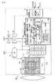
図1は、第1の実施形態に係るCMOSイメージセンサの概略構成をレンズとともに示すブロック図である。このCMOSイメージセンサは、センサ部11、ラインメモリ12、色相関RGB生成回路13、信号処理回路14、システムタイミング発生回路(SG)15、コマンドデコーダ16、およびシリアルインタフェース(シリアルI/F)17を備えている。18は、集光した光信号をセンサ部11に入力するレンズである。<First Embodiment>
FIG. 1 is a block diagram showing a schematic configuration of the CMOS image sensor according to the first embodiment together with a lens. The CMOS image sensor includes a
センサ部11には、画素部111およびカラム型アナログデジタルコンバータ(ADC)112が配置されている。画素部111は、画素が半導体基板上に行および列の二次元的に配置されたアレイを有する。各画素は、光電変換手段(例えばフォトダイオード)と色フィルタから構成され、フォトダイオードの受光面の前面にはR(赤)、G(緑)、B(青)の3色のカラーフィルタが配置される。色フィルタ配列は、ここではRGB原色のベイヤー配列を有する色フィルタを用いている。 The
センサ部11は、レンズ18を介して入力した被写体の光信号をカラーフィルタでRGB成分の光信号に分離し、フォトダイオードアレイで光電変換により信号電荷を生成する。この信号電荷は、カラム型ADC112でデジタル的な信号(R信号、G信号、B信号)に変換され、出力される。センサ部11から出力した信号は、ラインメモリ12に入力される。ここでは色フィルタ配列がADC112に対して7列並列に配置されているので、システムタイミング発生回路15からのクロックにより、この7列の色フィルタに対応する7列のフォトダイオードアレイからのセンサ出力が順次出力され、ラインメモリ12内の7ライン分のラインメモリ1〜ラインメモリ7に順次記憶される。このメモリ1〜メモリ7に記憶された信号は、システムタイミング発生回路15からのクロックにより色相関RGB生成回路13へ順次並列に出力される。 The
色相関RGB生成回路13は、第1の加算部131、平均比率算出部132、RGB生成部133、エッジ処理部134、信号合成部135、バンドパスフィルタ(BPF)136、振幅強調部137、G補間・輪郭処理部130、輪郭信号抽出部139などを有する。 The color correlation
第1の加算部131では、ラインメモリ12から並列に入力された信号(R信号、G信号、B信号)に基づいて第1の加算信号Sを生成する。そして、平均比率算出部132では、加算画素の周辺画素の色情報に基づいて、R信号、G信号、B信号の各々と第1の加算信号Sとの平均比率係数を算出する。そして、RGB生成部133では、平均比率係数と第1の加算信号Sとから、画素配列の同じ位置の信号として新たなRs、Gs、Bs信号を生成する。このRs、Gs、Bs信号はベイヤー配列で生成してもよい。このような処理は従来の色分離補間回路における処理の代わりとなり、エッジ部分の色ずれや色ノイズを抑圧する。 The
RGB生成部133で処理されたRs、Gs、Bs信号は、後段の信号処理回路14に入力され、ホワイトバランス、輪郭強調、ガンマ(γ)補正、およびRGBマトリックス回路などにより処理され、YUV信号形式やRGB信号形式のデジタル信号DOUT0〜DOUT7として出力される。また、前述したセンサ部11、ラインメモリ12に加えて、色相関RGB生成回路13および信号処理回路14の動作も、システムタイミング発生回路(SG)15から出力されるクロック信号に基づいて行われる。この際、各回路の処理のパラメータなどをコマンドにより制御することもできる。例えば、外部から入力されるデータDATAがシリアルインタフェース(シリアルI/F)17を介してコマンドデコーダ16に入力され、デコードされた信号がシステムタイミング発生回路15、ラインメモリ12、色相関RGB生成回路13、信号処理回路14に入力されることにより、外部入力データDATAにより処理のパラメータなどを制御することもできる。 The Rs, Gs, and Bs signals processed by the
ところで、第1の加算部131において、ラインメモリ12から並列に入力された信号の4画素分以上(ここでは、3×3画素配列の9画素分)を加算して第1の加算信号Sが生成される。この加算信号Sは画素ピッチに対応する高周波成分を含んでいないので、エッジ信号がなだらかになる。そこで、第1の加算信号Sの傾斜部分の信号変化が所定の基準より緩やかな場合を検出して信号変化を急峻にするためのボケ補正処理をボケ補正回路140にて実施する。また、第1の加算部131による加算処理と並行して、まず、G補間・輪郭処理部130において、加算前の信号に対してG補間処理および輪郭処理を実施する。そして、上記したG補間処理を実施した信号から高周波成分のS輪郭信号(高解像度信号)をS輪郭信号抽出部139で抽出し、このS輪郭信号を信号合成部135で加算部131からの第1の加算信号Sに加算もしくは乗算して合成信号Saを生成する。 By the way, in the
さらに、ボケ補正部140からの第1の加算信号Sからバンドパスフィルタ(BPF)136により中間の周波数を抜き出して振幅強調部137で振幅強調した後に信号合成部135で第1の加算信号Sに加算もしくは乗算することが望ましい。これにより、第1の加算信号Sの中間周波数のMTFの変調度を向上させ、解像度感を向上させることができる。 Further, an intermediate frequency is extracted from the first addition signal S from the
なお、回路132における平均比率係数の算出に際して、信号の切り替わりのエッジでの比率係数の誤差により色再現性が劣化するおそれがある。この劣化の対策として、ラインメモリ12から入力された信号の比率係数を高(Hi)レベル,中(Mid)レベル,低(Lo)レベルに分離して算出し、比率係数のHiレベルもしくはLoレベルをエッジ処理部134で選択して新たなR信号、G信号、B信号を生成している。この比率係数の選択は、回路139からのS輪郭信号および回路140からのボケ補正処理より抽出した信号に基づいて切り換えている。 When calculating the average ratio coefficient in the
上記した第1の実施形態によれば、各画素の信号に単独画素に起因するランダムノイズが存在しても、回路131において3×3画素配列に対して第1の加算信号Sを生成することにより、第1の加算信号Sではランダムノイズが低減され、S/Nを向上させることができる。また、各画素と同位置の画素の信号として、共通の第1の加算信号SからRs,Gs,Bs信号を生成することにより、Rs,Gs,Bs信号のランダムノイズ成分が同じとなる。したがって、デモザイキングによる偽色抑圧回路が不要となり、エッジに起因する偽色を抑制できる。すなわち、輝度ノイズしか発生しないので、単色の色ノイズを抑圧することができる。 According to the first embodiment described above, the
また、1つの加算信号SからRs,Gs,Bs信号を生成しているので、信号処理回路14において色再現性を改善するためのカラーマトリックス演算により信号を減算処理して新たにRGB信号を生成しても、各信号に含まれるランダムノイズが同位相となり、ノイズは増加しない。 In addition, since the Rs, Gs, and Bs signals are generated from one addition signal S, the
さらに、第1の加算信号Sの中域周波数成分を抽出して振幅強調部137で振幅強調した信号を第1の加算信号Sに加算することにより解像度感を向上させることができる。 Further, the sense of resolution can be improved by extracting the middle frequency component of the first addition signal S and adding the signal whose amplitude is enhanced by the
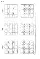
図2(B)は、図1中の色相関RGB生成回路13において前述したG信号の補間処理を行うG補間処理回路130の動作の一例を示す。ここでは、R,B画素位置にそれぞれG信号を生成する。以下、図2(A)に示す3×3画素配列の中心位置のR3画素(補間対象)の位置に補間用のG信号gmを生成する方法を図2(B)に示す。まず、R3画素に隣接する4つのG画素(=G1,G2,G4,G5 画素)の信号レベルの最大値(Gmax)と最小値(Gmin)を判定し、ステップS1においてその差分の信号Gd(=Gmax-Gmin)を求める。ステップS2においてこの差分信号Gdを所定の判定レベルLevNと比較し、GdがLevNより小さいと判定した場合、ステップS5においてG信号gmとして4つのG信号の平均値=(G1+G2+G4+G5)/4を生成する。上記判定レベルLevNは、ランダムノイズレベルを想定している。差分信号GdがLevNより大きいと判定した場合、次のステップS3においてさらに、R3画素に縦方向に隣接する2つのG1,G5画素の信号の差分信号の絶対値ABS(G1-G5)をLevNと比較し、ABS(G1-G5)がLevNより小さいと判定した場合は、ステップS6においてG1,G5画素の信号の平均値=(G1+G5)/2を生成して補間する。これに対して、ABS(G1-G5)がLevNより大きいと判定した場合はステップS4に移行し、R3画素に横方向に隣接する2つのG2,G4画素の信号の差分の絶対値ABS(G2-G4)がLevNより小さいか否かの判定を行なう。絶対値ABS(G2-G4)がLevNより小さいと判定した場合は、ステップS7においてG2信号とG4信号の平均値=(G2+G4)/2を生成して補間する。R3画素の縦方向、横方向に相関がない場合には、ステップS8に進み、R3画素の周辺のR1,R2,R4,R5画素の信号とR3画素の信号の差分信号の絶対値ABS(R1-R3)=R13,ABS(R2-R3)=R23,ABS(R4-R3)=R43,ABS(R5-R3)=R53を算出する。この4つの差分信号の絶対値(R13,R23,R43,R53)の算出の結果から、ステップS9において差分信号が最小Rminである画素の位置(最小画素位置)を決定する。そして、G信号gmとして、最小画素位置と同じ方向の画素の信号を用いる
。例えば、R3画素の周辺のR1,R2,R4,R5画素の中でR2画素の信号とR3画素の信号の差分が一番小さい場合には、R2画素とR3画素の中間に位置するG2画素の信号で補間する。このような処理により、高解像度のG信号gmを補間することができる。FIG. 2B shows an example of the operation of the G
なお、4つの差分信号の絶対値(R13,R23,R43,R53)が全てLevNより小さい場合は、4つのG信号の平均値=(G1+G2+G4+G5)/4で補間することによりS/Nを改善することができる。このG補間処理の方法は、本例以外も適用できる。 If the absolute values (R13, R23, R43, R53) of the four difference signals are all smaller than LevN, the average value of the four G signals = (G1 + G2 + G4 + G5) / 4 S / N can be improved. This G interpolation processing method can be applied to other than this example.
ここで、G補間処理回路130は図2(B)に示すフローチャートで表された動作を行なうようにプログラミングされたソフトウエアを用いて実行するコンピュータであってもよく、或いは図2(B)に示された各ステップの動作を行なうように組み立てられた独立の回路を組み合わせて構成してもよい。また、以下に順次動作方法を説明する色相関GBR生成回路13内の各ブロック回路もその方法を実現するように構成したソフトウエアを用いてコンピュータにより実現してもよいし、あるいはディスクリート回路の組み合わせにより構成された回路を用いてもよい。 Here, the G
図3は、図1中の色相関RGB生成回路13においてG輪郭信号を生成する方法の一例を示す。図2(B)に示した方法により補間のために生成したG信号を用いて、G輪郭信号を生成する。例えば図3に示す5×5画素配列P31内の太線内の3×3画素配列P32の中心位置のG33画素に対しては、G33画素の信号レベルを8倍し、G22、g23、G24、g32、g34、G42、g43、G44画素の各信号レベルを−1倍して加算した信号G33'をG輪郭信号として生成する。このG輪郭信号G33'は、均一被写体では発生せず(零)、センサ11の表面に縦縞、横縞などのパターンが発生した場合に発生する。他の輪郭生成方法として、G信号を低周波領域通過フィルタ(LPF)で高周波信号を除去し、元の高周波信号を含んだG信号との割り算を実施することで、LPFより低い低周波領域では結果が1となる。LPFより高い高周波信号は1より大きいかもしくは小さい結果が得られる。よって、割り算の結果が1以外となる信号が高周波信号であり、この信号を輪郭信号として抽出することができる。この抽出した信号を最適な輪郭信号レベルに振幅調整し、元の信号に乗算することで輪郭強調した合成信号が生成できる。輪郭信号の生成方法は、さらに他の方法も適用できる。 FIG. 3 shows an example of a method for generating a G contour signal in the color correlation
図4および図5は、図1中の色相関RGB生成回路13における基本的な処理方法および被写体のエッジ領域(被写体から得た信号が急激に変化する領域)に対して実施する処理方法の一例を示す。 4 and 5 show an example of a basic processing method in the color correlation
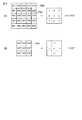
まず、5×5画素配列もしくは7×7画素配列の中心画素(T画素)(ここでは5×5画素配列P41内の中心画素:T画素)を中心に3×3画素配列P42のフィルタ演算を実施する。この際、図示したように、3×3画素配列P42のT画素の信号を4倍し、T画素に隣接する上下左右の画素の信号を2倍し、3×3画素配列のコーナー部の画素の信号を1倍とし、これらを合計した信号レベルを1/16にする。こうして得られた信号をT画素の加算信号S0とする。その後、加算信号S0にBPF136からの信号とS輪郭回路からの信号とを合成部135で合成してSa信号を生成する。 First, the filter operation of the 3 × 3 pixel array P42 is performed around the center pixel (T pixel) (here, the center pixel in the 5 × 5 pixel array P41: T pixel) of the 5 × 5 pixel array or the 7 × 7 pixel array. carry out. At this time, as shown in the figure, the signal of the T pixel in the 3 × 3 pixel array P42 is quadrupled, the signal of the upper, lower, left and right pixels adjacent to the T pixel is doubled, and the pixel at the corner of the 3 × 3 pixel array Is multiplied by 1 and the total signal level is 1/16. The signal thus obtained is referred to as a T pixel addition signal S0. Thereafter, the signal from the
一方、加算信号S1〜S8の平均値Saveを生成し、RGBベイヤー配列からなる5×5画素配列もしくは7×7画素配列(ここでは5×5画素配列)の各信号中の同じ色の画素信号の平均値をそれぞれRave、Gave、Baveとして算出する。信号Saveは、Hi、Mid、Loの各Rave、Gave、Baveを加算した信号とする。そして、被写体画像のエッジ部分の信号(エッジ信号)をエッジ処理部134により検出し、エッジ部分にエッジ処理を実施する。エッジ処理に際しては、5×5画素配列もしくは7×7画素配列(ここでは5×5画素配列)の同色の全信号の平均値を比率係数として単純に用いるのではなく、R信号、G信号、B信号の比率係数を大,中,小レベルに分離して算出し、信号のエッジ領域では信号の大レベルもしくは小レベルに対応して算出した比率係数を用い、信号の平坦領域では中レベルに対応して算出した比率係数を用いる。 On the other hand, an average value Save of the addition signals S1 to S8 is generated, and pixel signals of the same color in each signal of a 5 × 5 pixel array or a 7 × 7 pixel array (in this case, a 5 × 5 pixel array) having an RGB Bayer array. Are calculated as Rave, Gave, and Bave, respectively. The signal Save is a signal obtained by adding Hi, Mid, and Lo Rave, Gave, and Bave. Then, the
上記したようにR信号、G信号、B信号の比率係数を大,中,小レベルに分離して算出する際、R,G,B信号のそれぞれの比率係数の並べ替え処理を行う。例えば図5に示すように、5×5画素配列P51の各画素RGBそれぞれの信号をそのレベルに従って小から大へ順に並べる。例えば画素Bについて最小レベル画素B1から最大画素B4の順に並べる。そして、Hiレベル2画素のR,G,Bの平均値Rave、Gave、Baveをそれぞれ算出する。ここで、3画素の平均値を算出してもよい。同様に、Midレベルの2画素もしくは3画素のR,G,Bの平均値Rave、Gave、Baveを算出する。ここでは画素RのMidレベルが3画素平均であり、他は2画素平均を算出している。同様に、Loレベルの2画素もしくは3画素のR,G,Bの平均値Rave、Gave、Baveを算出する。そして、加算信号の平均値Saveは、図4に示すようにそれぞれのHi,Mid,Loレベルの各平均値を加算(Save=Rave+Gave+Bave)して算出する。なお、上記したエッジ領域に対する処理の対象となる画素数は、2画素、3画素に限定されない。 As described above, when the ratio coefficients of the R signal, the G signal, and the B signal are calculated separately for the large, medium, and small levels, the ratio coefficients of the R, G, and B signals are rearranged. For example, as shown in FIG. 5, the signals of each pixel RGB of the 5 × 5 pixel array P51 are arranged in order from small to large according to the level. For example, the pixels B are arranged in the order of the minimum level pixel B1 to the maximum pixel B4. Then, average values Rave, Gave, and Bave of R, G, and B of
そして、上記平均値Rave、Gave、Baveおよびこれらを加算した平均値Saveに基づいて第2の加算信号Saに対応した3つの比率係数Ka(=Rave/Save,Gave/Save,Bave/Saveを算出する。そして、RGB生成部133により、信号KaとSaを用いて新たな信号Rs(=Sa*Rave/Save)、Gs(=Sa*Gave/Save),Bs(=Sa*Bave/Save)を生成する。この際、S輪郭信号がHi(プラス)の時には、Hiレベルの比率係数を用いて新たにRs,Gs,Bs信号を生成する。S輪郭信号がLo(マイナス)の時には、Loレベルの比率係数を用いて新たにRs,Gs,Bs信号を生成する。このようにS輪郭信号のHi、Loを算出してRs,Gs,Bs信号を生成処理することにより、色収差によってR,G,Bの最高の解像度が得られる位置がずれていてもエッジ領域の偽色信号発生を抑圧することができる。 Then, three ratio coefficients Ka (= Rave / Save, Gave / Save, Bave / Save) corresponding to the second addition signal Sa are calculated based on the average values Rave, Gave, Bave and the average value Save obtained by adding them. Then, the
図6(A)〜図6(H)は、図1中の色相関RGB生成回路13内のボケ補正回路140において第1の加算信号Sのボケ補正を行う処理の一例を示す。図6(A)は、センサ部11内の画素によって表される信号イメージを示しており、斜線部分は加算処理により信号波形が緩やかに傾斜しているエリアを示している。図6(A)中のG−G´線に沿う画素列に対応して示すG−G´信号波形のように、図中左側(G側)から図中右側(G'側)へ緩やかに信号レベルが上昇している。ここで、図6(B)に示すように、3×3画素配列P61内の中心領域の画素に着目し、10×10画素配列P62の中心位置(5,E)の画素の信号をD0とし、斜め4方向に隣接する画素の信号をD1〜D4とする。そして、このD1〜D4について図6(C)に示すような判定条件により傾斜判定を実施する。すなわち、D0との差分が所定の判定レベルLevNより小さい場合は、図6(D)に示すように7×7画素配列P63において傾斜がない場合と判定して0(零)とし、傾斜がある場合を1とする。このような傾斜判定の結果に基づいて、まず、この7×7画素配列P63内の中央部の3×3画素配列のエリアで0の有無を判定する。0が無い場合は判定エリアを5×5画素配列に広げる。最大エリアは自由に設定できる。この5×5画素配列に0がある場合は、この0の位置の信号と置換する。0が複数画素ある場合は、平均値処理やメディアン処理を行って置換する。0の信号が大信号(5×5画素配列に対応)と小信号(3×3画素配列に対応)に含まれる場合は、含まれる個数が多い方を選択する。この処理を順次選択することにより、図6(E)に示すように緩やかな傾斜を改善した信号が得られる。もし、図6(D)中の5×5画素配列のエリアに0が無い場合は、加算処理で発生した傾斜でなく、元来の被写体自身の緩やかな傾斜と判断し、信号を置換せずにそのまま用いる。 6A to 6H show an example of processing for performing blur correction of the first addition signal S in the
図6(F)は、比率係数のHi,Lo判定方法の一例を示す。図6(D)の判定結果1の信号D(1)に対して、周辺判定結果0の信号D(0)との大小判定を実施し、D(0)が大きい場合は+1とし、小さい場合は-1と判定する。その結果、G-G'の比率係数は図6(G)に示すようになり、例えば図6(H)に示すG−G´信号波形のように、判定結果0,-1,+1,0…に応じてMid,Lo,Hi,Mid,…で使う係数が定まる。 FIG. 6F shows an example of a Hi / Lo determination method for the ratio coefficient. The signal D (1) of the
図7(A)〜図7(J)は、図1に示したCMOSイメージセンサにおける各部の信号処理の流れを示す。ここでは、信号処理の原理を判り易くするために、センサ部11から出力されるR,G,B信号は同位相で出力されているように1ライン分を抜き取った信号波形を示している。この信号を水平方向に1,2,1の重み付けでフィルタ処理を行い、S/Nが改善された信号Sを得る。しかし、この信号Sは、信号の切り換わりエッジ部分が緩やかになってしまうため、限界解像度の領域では変調度が零となり、信号変化が検出できない。 FIG. 7A to FIG. 7J show the flow of signal processing of each part in the CMOS image sensor shown in FIG. Here, in order to easily understand the principle of signal processing, R, G, and B signals output from the
そこで、図2(A),2(B)および図3を参照して前述したように生成されたG輪郭信号をS輪郭信号として用いている。そして、このS輪郭信号を信号Sに加算することで、元のG信号と同じ高解像度のSa信号が得られる。この際、S輪郭信号の信号レベルは、解像度感に対応して調整するようにしてもよく、S輪郭信号のレベルを大きくして加算することにより、輪郭強調の効果が得られる。 Therefore, the G contour signal generated as described above with reference to FIGS. 2A and 2B and FIG. 3 is used as the S contour signal. Then, by adding this S contour signal to the signal S, a Sa signal having the same high resolution as the original G signal can be obtained. At this time, the signal level of the S contour signal may be adjusted in accordance with the sense of resolution, and the effect of contour emphasis can be obtained by increasing and adding the level of the S contour signal.
また、前述したようにセンサ部11から出力されるRGB信号は、レンズ18による色収差のために信号位相がずれて出力されている。S輪郭信号は、前述したG輪郭信号を用いているが、小さな輪郭信号レベルはノイズと判断し、S輪郭信号から削除し、大きな信号のみをS輪郭信号としている。また、輪郭レベルを調整してS信号に加算している。加算した信号Sは、RGBの各信号を加算している。このため、図7(E)に示すように、低周波領域では、信号変化部分で信号の傾斜が緩やかになっており、高周波領域では、信号の変化レベル(変調度)が小さくなっている。S信号にボケ補正を実施した図7(F)に示すSb信号は、低周波領域のエッジボケを改善している。高周波領域では、緩やかな傾斜となっていないので、S信号がそのまま出力される。このSb信号にS輪郭信号を加算した図7(G)に示す信号Saは、信号のエッジ部分が強調されて、解像度感を改善している。 Further, as described above, the RGB signal output from the
図6(A)〜図6(H)中に示したように生成した信号とS輪郭信号から得られた極性を合成した信号は、比率係数選択信号となっており、この信号に基づいて、信号波形のHi,Mid,Loの比率係数Kaを決定している。 A signal obtained by combining the signal generated as shown in FIGS. 6A to 6H and the polarity obtained from the S contour signal is a ratio coefficient selection signal. Based on this signal, The ratio coefficient Ka of Hi, Mid, Lo of the signal waveform is determined.
ここで、エッジ領域の比率係数の選択方法の一例を説明する。図7(D)に示すS輪郭信号レベルがプラスもしくはマイナスの時はエッジ部分であると判定できる。S輪郭信号レベルが零の時は、エッジ部分でないと判定できる。この判定に基づいて、図4に示すエッジ処理回路134において、比率係数の中からS輪郭信号がプラスの時にはHiレベルの平均値(Hi-ave)の比率係数を選択し、S輪郭信号がマイナスの時にはL0レベルの平均値(L0-ave)の比率係数を選択し、S輪郭信号が零の時にはMidレベルの平均値(Mid-ave)の比率係数を選択する。S輪郭信号が所定レベルより小さい時は、信号無し(零)と判定している。S輪郭信号が所定レベルより大きい時は、輪郭信号有りと判定し、プラスもしくはマイナスの信号を有効にしている。なお、上記とは別の処理方法として、低域のエッジ領域でエッジ信号を判定した時には、図2(B)で算出した比率係数は隣接の比率係数で補間処理することもできる。 Here, an example of a method for selecting the ratio coefficient of the edge region will be described. When the S contour signal level shown in FIG. 7D is positive or negative, it can be determined that it is an edge portion. When the S contour signal level is zero, it can be determined that it is not an edge portion. Based on this determination, in the
次に、Sa信号と3つの係数KaからRs,Gs,Bs信号を生成する。この結果、元のG信号が持つのとほぼ同じ解像度情報が生成される。さらに、図7(C)および図7(J)から明らかなように、Bs,Rs信号のエッジはGs信号と位相が同じになるので色偽信号は発生しない。また、Rs,Gs,Bs信号のランダムノイズとR,G,B信号は相関を持っている(同位相となる)。すなわち、ランダムノイズでG信号レベルが大きくなれば、R,B信号とも大きくなり、ランダムノイズでG信号レベルが小さくなればR,B信号とも小さくなる。したがって、従来発生していた色ノイズ(ドット状のランダムノイズ)を抑圧することが可能になり、ノイズは輝度ノイズのみとなる。 Next, Rs, Gs, and Bs signals are generated from the Sa signal and the three coefficients Ka. As a result, almost the same resolution information as that of the original G signal is generated. Further, as apparent from FIGS. 7C and 7J, the edges of the Bs and Rs signals have the same phase as the Gs signal, so that no color false signal is generated. Further, the random noise of the Rs, Gs, Bs signals and the R, G, B signals have a correlation (being in phase). That is, if the G signal level increases due to random noise, both the R and B signals increase. If the G signal level decreases due to random noise, both the R and B signals decrease. Accordingly, it is possible to suppress color noise (dot-like random noise) that has been generated conventionally, and the noise is only luminance noise.
図8(A)および図8(B)は、図1中の色相関RGB生成回路13において第1の加算信号Sの中周波数領域(中域)の信号振幅を拡大(強調)する方法の一例を示す。図8(A)では、第1の加算信号SからBPF処理を用いて中域信号を抜き出す方法を示す。例えば、5×5画素配列P81内の3×3画素エリアP82の中心画素の信号S33に、3×3画素エリアP82の各画素に対応した係数(4、2、1)を掛け算し、加算する。そして、加算の前後で信号レベルが同じになるように、加算後に1/16にし、この強調信号を新たに中心画素の信号S33'とする。 FIGS. 8A and 8B are examples of a method of enlarging (emphasizing) the signal amplitude in the middle frequency region (middle region) of the first addition signal S in the color correlation
図8(B)は、3×3画素エリアP82中の各画素に対して上記と同様に処理して強調信号を生成する方法を示す。このように生成した信号に、図3を参照して前述したと同様の輪郭抽出処理をすることによって中域の強調信号S33''を抽出する。この信号S33''を、図1中の振幅強調部137で振幅を制御して元の第1の加算信号Sに加減算する。これにより、中域周波数の振幅が増加し、解像度感が向上する。このように振幅強調を実施しても、本実施形態では、色バランスは平均比率算出で別に実施しているので、色再現性は変化しない。 FIG. 8B shows a method of generating an enhancement signal by processing each pixel in the 3 × 3 pixel area P82 in the same manner as described above. The signal generated in this manner is subjected to contour extraction processing similar to that described above with reference to FIG. 3, thereby extracting the mid-range enhancement signal S33 ″. The signal S33 ″ is added to or subtracted from the original first addition signal S by controlling the amplitude by the
<第2の実施形態>
図9は、第2の実施形態に係るCMOSイメージセンサの概略構成を示すブロック図である。前述したようにレンズ18でピントボケした画像から得られる入力信号は高解像度の信号ではない。そこで、第2の実施形態のCMOSイメージセンサでは、レンズ18のピントボケの対策を実施しており、前述した第1の実施形態の色相関RGB生成回路13と比べて、一部が異なる色相関RGB生成回路13aが用いられる。<Second Embodiment>
FIG. 9 is a block diagram showing a schematic configuration of a CMOS image sensor according to the second embodiment. As described above, the input signal obtained from the image that is out of focus by the
以下、異なる部分を主として説明する。色相関RGB生成回路13aにおいて、加算回路131からの第1の加算信号Sに補正回路140でボケ補正処理を施したSb信号をスイッチ素子141により選択してS輪郭回路139に導き、これを用いてSa輪郭信号を生成している。この補正回路140からのSb信号を用いることで、高いS/Nを有する輪郭信号が生成される。勿論、第1の実施形態と同様に、補間処理回路130からのG信号をスイッチ素子141により選択してS輪郭回路139に与えて形成した信号を用いても良く、さらには、Sb信号からの輪郭信号とG信号からの輪郭信号を合成してS輪郭信号に用いても良い。他の回路は図1に示したものと同じであり、重複する説明は省略する。 Hereinafter, different parts will be mainly described. In the color correlation
上記図9に示した第2の実施形態によれば、前述した第1の実施形態と同様の効果が得られる。しかも、図11(A)、図11(B)を参照して後で述べるRGBの焦点位置の異なるレンズ18aを使用する場合でも、信号処理によって擬似的に被写界深度を深くすることができる。 According to the second embodiment shown in FIG. 9, the same effects as those of the first embodiment described above can be obtained. Moreover, even when a
<第3の実施形態>
図10は、第3の実施形態に係るCMOSイメージセンサの概略構成を示すブロック図である。このCMOSイメージセンサは、S輪郭として、Sb信号から生成した輪郭信号SbをRGB信号から生成したR輪郭信号,G輪郭信号,B輪郭信号と合成し、これをS輪郭合成信号として用いている。レンズ18aは、レンズ設計で発生する軸上色収差(図11(A)参照)を有するが、この軸上色収差を積極的に活用している。すなわち、図11(B)に示すように、光入力のB成分のピント位置を30cm前後とし、G成分のピント位置を50cm〜1m、R成分のピント位置を1m以上の被写界深度が得られるようにレンズ18aを設計している。そして、光信号の各BGR のピント位置をずらすことによって、被写界深度を異ならせている。<Third Embodiment>
FIG. 10 is a block diagram showing a schematic configuration of a CMOS image sensor according to the third embodiment. This CMOS image sensor combines the contour signal Sb generated from the Sb signal with the R contour signal, G contour signal, and B contour signal generated from the RGB signal as the S contour, and uses this as the S contour combined signal. The
このCMOSイメージセンサでは、図12に示すように、まず、各RGB信号の5×5画素配列P121、P122、P123の夫々について3×3画素配列における補間処理(中心画素を上下左右の4画素の平均値で埋める処理)を図示のように実施する。この補間した各画素信号から図2(B)あるいは図3と同様の処理により各RGB信号の輪郭信号を抽出する。抽出した信号を加算することで、近い被写体から遠くの被写体まで解像度感のある信号が得られる。 In this CMOS image sensor, as shown in FIG. 12, first, interpolation processing in a 3 × 3 pixel array for each of the 5 × 5 pixel arrays P121, P122, and P123 of each RGB signal (the center pixel is made up of four pixels on the top, bottom, left, and right). The process of filling with the average value is performed as shown in the figure. A contour signal of each RGB signal is extracted from each interpolated pixel signal by the same processing as in FIG. 2B or FIG. By adding the extracted signals, a signal with a sense of resolution can be obtained from a near subject to a far subject.
第3の実施形態によれば、前述した第1の実施形態と同様の効果が得られる。しかも、図11(A),図11(B)に示す軸上色収差を有する通常のレンズ18aを用いても、信号処理により被写界深度を深く設定することができる。 According to the third embodiment, the same effects as those of the first embodiment described above can be obtained. Moreover, the depth of field can be set deeper by signal processing even when the
<第4の実施形態>
図13は、第4の実施形態に係るCMOSイメージセンサの概略構成を示すブロック図である。第4の実施形態は、前述した第3の実施形態と比べて、レンズ18aは同じものを採用しているが、センサ部11bの一部、色相関RGB生成回路13bの一部が異なる。<Fourth Embodiment>
FIG. 13 is a block diagram showing a schematic configuration of a CMOS image sensor according to the fourth embodiment. The fourth embodiment employs the
以下、異なる部分を主として説明する。センサ部11bの色フィルタ配列は、4×4配列のWRGBフィルタを基本とした原色フィルタ111を用いており、WフィルタはRGBの信号を透過する色フィルタである。これにより、センサ部11bは、レンズ18aで集光した光信号をW,R,G,B信号に分離し、二次元のフォトダイオードアレイで信号電荷に変換させ、ADC112でデジタル信号に変換して出力する。 Hereinafter, different parts will be mainly described. As the color filter array of the
なお、図13に示すように、RGBフィルタ夫々の上下左右をWフィルタで囲む配列となるように、Wフィルタを市松模様に配置しておくことにより、色相関RGB生成回路13bでは、フィルタ111内の4×4画素配列の内のどの組み合わせでもWRGB画素の個数が同じ加算信号Sを得ている。また、補間回路130WによるW信号の補間処理、輪郭回路139WによるW信号の輪郭抽出を実施して、合成回路139SによりS輪郭信号を得ている。これにより、被写体の位置に応じて、W信号の輪郭情報として、近い被写体はB信号から、遠い被写体はR信号からの輪郭信号を抽出している。 As shown in FIG. 13, the color correlation
第4の実施形態によれば、前述した第1の実施形態と同様の効果が得られる。この際、W画素を用いることにより、S信号量が増加するので、撮像感度が向上する。 According to the fourth embodiment, the same effects as those of the first embodiment described above can be obtained. At this time, by using the W pixel, the amount of S signal is increased, so that the imaging sensitivity is improved.
<その他の実施形態>
上述した各実施形態では、5×5の画素配列と7×7の画素配列を例にとって説明したが、画素数をさらに増加させることで、さらに高いS/N、高画質化を実施できる。<Other embodiments>
In each of the above-described embodiments, a 5 × 5 pixel array and a 7 × 7 pixel array have been described as examples. However, by further increasing the number of pixels, higher S / N and higher image quality can be implemented.
また、輪郭信号の幅を大きく抽出したり(複数画素分)、複数画素分の大きな幅と小さな(例えば1画素分)幅の信号を合成した輪郭信号を用いることで、ボケ補正回路を用いずに同等のボケ補正効果を得ることができる。 In addition, a blur correction circuit is not used by extracting a large width of the contour signal (for a plurality of pixels) or by using a contour signal obtained by combining signals having a large width and a small width (for example, one pixel) for a plurality of pixels. The same blur correction effect can be obtained.
なお、カラーカメラのS/Nの劣化の要因の1つであるRGBマトリックス回路は、RGBの色再現性を改善するために、RGBの行列演算を例えば次の演算式で実施している。
この処理は、1つの色に対して他の2色を減算している。すなわち、1つの色に他の2色が混色している量を減算することで、1つの色の純度を高めて色再現性を改善している。上記混色の要因には、色フィルタ自身の分光特性や、センサのフォトダイオードまでの光学的なクロストークや、センサ部のシリコン基板内での信号の拡散要因などがある。従来はRs,Gs,Bsの信号のノイズがランダムであるので、上記減算処理によってノイズ量が増加していた。 In this process, the other two colors are subtracted from one color. That is, by subtracting the amount of the other two colors mixed with one color, the purity of one color is increased and the color reproducibility is improved. The color mixing factors include spectral characteristics of the color filter itself, optical crosstalk to the sensor photodiode, signal diffusion factors in the silicon substrate of the sensor unit, and the like. Conventionally, since the noise of Rs, Gs, and Bs signals is random, the amount of noise has been increased by the subtraction process.
これに対して、本発明の実施形態では、Rs,Gs,Bsのランダムノイズが同一成分であるので、上記減算処理によってランダムノイズを低減する効果がある。例えば、R信号を生成する時、ランダムノイズによってRs信号が大きくなった時、信号Gs、Bsも大きくなっている。行列演算により、R信号はRs信号からGs,Bs成分を減算するので、ランダムノイズが大きい分、大きな信号を減算する。よって、R信号はより大きな信号を減算している。上記とは逆に、ランダムノイズによってRs信号が小さく時、信号Gs、Bsも小さくなる。行列演算により、R信号はRs信号からGs,Bs成分を減算するが、ランダムノイズが小さい分、小さな信号を減算する。よって、R信号は信号の低下が小さい。この結果、R信号はランダムノイズを小さくする効果がある。同様に、G,B信号のランダムノイズも小さくなる。 On the other hand, in the embodiment of the present invention, since the random noise of Rs, Gs, and Bs is the same component, there is an effect of reducing the random noise by the subtraction process. For example, when the R signal is generated, when the Rs signal is increased due to random noise, the signals Gs and Bs are also increased. Since the R signal subtracts the Gs and Bs components from the Rs signal by matrix operation, a larger signal is subtracted as the random noise is larger. Therefore, the R signal is subtracted from a larger signal. Contrary to the above, when the Rs signal is small due to random noise, the signals Gs and Bs are also small. The R signal subtracts the Gs and Bs components from the Rs signal by matrix operation, but subtracts a small signal as the random noise is small. Therefore, the signal drop of the R signal is small. As a result, the R signal has the effect of reducing random noise. Similarly, the random noise of the G and B signals is also reduced.
また、本発明の撮像装置は、色フィルタ配列が異なったCMOSイメージセンサに適用した場合でも、RGB信号を生成した後に、同様の加算信号Sの生成とRGBの比率算出に基づいて新たなRs,Gs,Bsを生成することにより、前記した効果と同じ効果が得られる。 In addition, even when the imaging apparatus of the present invention is applied to CMOS image sensors having different color filter arrangements, after generating RGB signals, new Rs, By generating Gs and Bs, the same effect as described above can be obtained.
また、本発明の撮像装置は、CMOSイメージセンサに限定されることなく、その他のCCD(電荷結合型)センサや積層型センサでも適用できるほか、センサとは別チップで形成される専用のISP(イメージシグナルプロセッサ)にも適用できる。 The image pickup apparatus of the present invention is not limited to a CMOS image sensor, but can be applied to other CCD (charge coupled type) sensors and stacked sensors, and a dedicated ISP (chip) formed on a separate chip from the sensor. It can also be applied to image signal processors.
また、本発明は、センサ部で例えば10ビットADCの信号を4画素分加算してS信号を生成する場合に適用すると、S信号は、加算処理により実質12ビットの高精度化が可能になり、実質の飽和信号量が4倍になる。さらに、4画素分の加算処理により、ランダムノイズは約1/2に低減する。このように飽和信号量が4倍、ノイズ低減が1/2になると、ダイナミックレンジ(飽和信号量/ランダムノイズ)を8倍に拡大することが可能になる。さらに、4×4画素配列の16画素分の加算を行うと、飽和信号量が16倍、ランダムノイズが1/4に低減し、ダイナミックレンジを64倍に拡大することが可能になる。したがって、微細画素で飽和信号量が低下したとしても、実質4画素分を加算すれば、飽和信号量も4倍されるので、飽和信号量が実質的に従来の1/4でも、従来と同じS/Nが得られる。 In addition, when the present invention is applied to the case where an S signal is generated by adding four pixels of a 10-bit ADC signal in the sensor unit, for example, the S signal can be increased in accuracy to substantially 12 bits by addition processing. The actual saturation signal amount is quadrupled. Furthermore, the random noise is reduced to about ½ by the addition process for four pixels. Thus, when the saturation signal amount is 4 times and the noise reduction is ½, the dynamic range (saturation signal amount / random noise) can be expanded to 8 times. Furthermore, when 16 pixels in a 4 × 4 pixel array are added, the saturation signal amount is reduced by 16 times, the random noise is reduced by 1/4, and the dynamic range can be expanded by 64 times. Therefore, even if the saturation signal amount is reduced by a fine pixel, if the substantial four pixels are added, the saturation signal amount is also quadrupled. Therefore, even if the saturation signal amount is substantially 1/4 of the conventional one, it is the same as before. S / N is obtained.
例えば、飽和信号量が10000eleの時には、ショットノイズ(飽和信号量の平方根)は100eleとなり、S/N=40dBが得られる。飽和信号量が2500ele の時には、ショットノイズは50ele となり、S/N=34dBとなる。しかし、本発明を適用すれば、4画素加算で信号量が4倍の10000eleとなり、この時のノイズは2倍しか増大しないので、100eleとなる。この結果、S/N=40dBが得られる。したがって、飽和信号量が実質的に1/4になっても、高いS/Nを期待することができる。 For example, when the saturation signal amount is 10000 ele, the shot noise (square root of the saturation signal amount) is 100 ele, and S / N = 40 dB is obtained. When the saturation signal amount is 2500 ele, the shot noise is 50 ele and S / N = 34 dB. However, if the present invention is applied, the signal amount becomes 4 times 10000 ele by adding 4 pixels, and the noise at this time increases only 2 times, so it becomes 100 ele. As a result, S / N = 40 dB is obtained. Therefore, even when the saturation signal amount is substantially ¼, a high S / N can be expected.
また、本発明の撮像装置は、レンズ18、18aの色収差による画質の劣化を回避できるので、レンズ18、18aのF値を小さくすることにより高感度化を実現することができる。また、レンズ18の高さを低く、言い換えるとレンズ18の厚さを薄くすることで、カメラモジュールの高さを低くすることができる。この結果、薄型の携帯電話機に対応した小型カメラモジュールを容易に実現することができる。 In addition, since the image pickup apparatus of the present invention can avoid deterioration of image quality due to chromatic aberration of the
また、上記実施形態では、RGB形式もしくはWRGB形式の単板カラーカメラを例にとって説明したが、プリズムを使って3原色のRGB信号を得る3板カラーカメラでも色収差が発生するので、上記実施形態と同様の原理で高感度化、色収差対策を実施することができる。また、本発明を白黒センサに適用して輪郭補正を行った場合には、信号の増大とノイズ低減により、感度を高め、ダイナミックレンジを拡大することができる。 In the above-described embodiment, a single-plate color camera in RGB format or WRGB format has been described as an example. However, chromatic aberration also occurs in a three-plate color camera that obtains RGB signals of three primary colors using a prism. High sensitivity and chromatic aberration countermeasures can be implemented with the same principle. In addition, when contour correction is performed by applying the present invention to a monochrome sensor, sensitivity can be increased and dynamic range can be expanded by increasing signals and reducing noise.
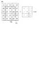
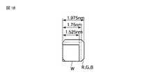
ここで、図13の実施例のWRGBのカラーフィルタ111の4×4画素配列P141を図14に示す。図15はこの縦方向の画素列WGWGにおけるセンサ部11の断面図、図16はこのWRGBの画素フィルタの分光特性を示す。図15において、カラーフィルタ111の前面にはレンズ18aの代わりにマイクロレンズ18bが画素ごとに設けられ、フィルタ111を通過した光は半導体基板であるSi基板150の表面領域に形成された画素ごとのフォトダイオードPDW,PDGの受光面に焦点を結んで入射される。 FIG. 14 shows a 4 × 4 pixel array P141 of the
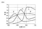
図16に示すように、Wの色フィルタは透明(白)なため、他のRGBフィルタより光強度のピークが高く、すべての成分を含むため、ダイオードPDWからはRGBの全領域の信号を得ることができる。しかし、Si基板150内で光電変換した信号電荷が拡散することで他の色の画素へ混入し混色が発生する。しかもW画素無しのRGBの分光特性に対して、信号レベルが持ち上がっている。この混色の影響で色が薄くなる。このため、色再現性を改善するためにカラーマトリックス係数を大きくすることで、色再現性を改善する。しかし、このマトリックス係数が大きいとS/Nが大きく劣化する。一般的に自分の信号から他の色の信号を減算するため、信号Sが小さくなり、ランダムノイズNが小さくならないためS/Nが劣化する。また、W画素の信号は、G画素の信号に対して約2倍得られる。そのため、W画素が飽和しない感度設定にすると、RGB信号は従来の1/2と小さくなるため、光ショットノイズで3dB劣化する課題がある。なお、Wの透明な色フィルタをグレー化することで感度を小さくできる。この結果、W画素からの混色を低減する方法がある。しかし、この方法はW画素を使った高感度のメリットが無くなるという問題を派生する。 As shown in FIG. 16, since the W color filter is transparent (white), it has a higher light intensity peak than other RGB filters and includes all components, so that signals of the entire RGB region are obtained from the diode PDW. be able to. However, the signal charges photoelectrically converted in the
<第5の実施形態>
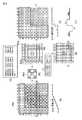
図17に、この問題を解決できる実施例のWRGBカラーフィルタの4×4画素配列P171を示す。この画素配列は、図18に示すように、市松状に配置したW画素の面積を小さくし、他のR,G,Bの面積を相対的に大きくしている。図19に水平方向に配列されたWGWG画素に対応するセンサ部11cの断面図を示す。PDW,PDGの受光面の面積は画素WRGBに対してすべて同じ面積になっている。この面積は、標準的な色温度を想定した場合に発生する信号電荷量に応じてサイズを最適化して良い。図17の平面図に示した画素Wに対応して、図19に示すように、マイクロレンズ18cと色フィルタWの面積を、色フィルタGのそれら(マイクロレンズ18c1,18c2と色フィルタGの面積)より小さく設定している。即ち、感度の高いW画素の面積を小さくし、W画素より感度の小さいGもしくはR,Bの面積を大きくしている。このように面積を異ならせることで、標準的な色温度例えば5500Kの時のW画素とG画素の信号量を同等にしている。W画素の高感度化のメリットをW画素に入射する面積を小さくし、他のR,G,B画素の面積を大きくすることで高感度化を実現できる。<Fifth Embodiment>
FIG. 17 shows a 4 × 4 pixel array P171 of WRGB color filters of an embodiment that can solve this problem. In this pixel arrangement, as shown in FIG. 18, the area of W pixels arranged in a checkered pattern is reduced, and the areas of other R, G, and B are relatively increased. FIG. 19 is a cross-sectional view of the
マイクロレンズの曲率は、面積が大きいR,G,B画素に対応するマイクロレンズ18c1,18c2を大きくし、面積が小さいW画素のマイクロレンズ18cの曲率を小さくしている。マイクロレンズの曲率を変えるには、例えば、マイクロレンズの形成をW画素では1回の塗布プロセスで形成し、面積の大きいR,G,B画素の部分では2回以上の塗布プロセスで形成することで実現できる。即ち、W画素でのマイクロレンズは1層からなり、R,G,B画素でのマイクロレンズは2層以上からなる。ここでは、W画素(画素面積小)が1層、R,G,B画素(画素面積大)が2層以上で説明しているが、R,G,B画素のマイクロレンズを形成する層がW画素のマイクロレンズを形成する層より多くの層によって形成されていればよい。図20に分光特性を示す。W画素の信号レベルを小さくし、その分R,G,B画素の信号が増加していることが分かる。入射するW画素の信号量が減少するため、波長550nm以上のR,Gの信号の裾野のレベル浮き(混色)が低減している。この結果、色再現性を改善するためのカラーマトリックス係数を小さくすることができ、S/Nの劣化を低減している。 As for the curvature of the microlens, the microlenses 18c1 and 18c2 corresponding to the R, G, and B pixels having a large area are enlarged, and the curvature of the
このように、高感度化のために用いる透明(白)の色フィルタはG信号の約2倍の感度を有する。よって、信号のバランスが崩れる問題や、W画素からのリークにより混色が大きくなり色再現性改善のためのカラーマトリックス係数が大きくなるためS/Nが劣化する問題が有ったが、本実施例は、高感度のW画素の面積を小さくし、その分を他のRGB色画素の面積を大きくすることで色信号のS/Nを改善するとともにWとG画素の信号レベルが同じになるように調整することができる。その結果、カラーマトリックス係数を小さくできるためS/Nの劣化を回避することができる。 Thus, the transparent (white) color filter used for high sensitivity has a sensitivity about twice that of the G signal. Therefore, there is a problem that the balance of signals is lost, and there is a problem that S / N deteriorates because color mixture increases due to leakage from W pixels and a color matrix coefficient for improving color reproducibility increases. Reduces the area of high-sensitivity W pixels and increases the area of other RGB color pixels accordingly, so that the S / N of the color signal is improved and the signal levels of the W and G pixels are the same. Can be adjusted. As a result, since the color matrix coefficient can be reduced, S / N degradation can be avoided.
即ち、W画素を小さくすることで、シリコン(Si)基板150内で発生する混色を低減できるためカラーマトリックス処理によるS/N劣化を低減できる。さらに、他のRGB画素の実効的な光の入射する面積を大きくすることにより、感度が高くなるためS/Nが改善できる。 That is, by reducing the W pixel, the color mixture generated in the silicon (Si)
図21(A)〜図21(C)に、この発明の実施に用いるレンズ構成の例を示す。図21(A)はレンズ開口絞りがF2.8の場合の一般的な焦点面の結像状態を示している。図21(B)に開口絞りがF2.0と小さくした場合を示す。一般に、F値を小さくすると焦点位置における入射光と光軸との角度が大きくなるため、焦点深度が狭くなるため焦点が合う被写体の距離が狭くなる。図21(C)に特に本発明の実施に好適な焦点深度を深くしたレンズの例を示す。レンズの球面収差を利用している。図21(C)では、F2.8のレンズ開口エリアよりF2.0を使ったときに広がる開口エリアの領域で中央エリアより焦点距離を長く設定することで焦点深度を深くしている。すなわちレンズの色収差とさらに球面収差を利用している。球面収差はレンズ形成時にリング状または上下もしくは左右で焦点距離を異ならせて形成することで実現できる。通常、開口F値を小さくすると焦点範囲が狭くなる、このため色収差をさらに低減するようにレンズ設計をすると、レンズ枚数が増加していた。図21(C)のレンズでは、逆に色収差を大きくすることで、焦点深度を深くすることができ、色収差を低減しなくて良いためレンズ枚数を少なくできる。レンズ枚数が少なくなることでカメラモジュールの高さも低くすることができる。更にレンズ絞りF2.0とすることでF2.8に対して約2倍の光量が得られるため(F値の2乗比で増加)高感度化が実現できる。 FIG. 21A to FIG. 21C show examples of lens configurations used in the practice of the present invention. FIG. 21A shows a general focal plane imaging state when the lens aperture stop is F2.8. FIG. 21B shows a case where the aperture stop is made as small as F2.0. In general, when the F value is decreased, the angle between the incident light and the optical axis at the focal position is increased, so that the depth of focus is reduced, and the distance of the subject in focus is reduced. FIG. 21C shows an example of a lens having a deep focal depth that is particularly suitable for implementing the present invention. It uses the spherical aberration of the lens. In FIG. 21C, the focal depth is deepened by setting the focal length longer than the central area in the area of the aperture area that is widened when using F2.0 than the lens aperture area of F2.8. In other words, the lens uses chromatic aberration and spherical aberration. Spherical aberration can be realized by forming a lens in a ring shape or by changing the focal length vertically or horizontally. Usually, when the aperture F value is decreased, the focal range is narrowed. For this reason, when the lens is designed to further reduce chromatic aberration, the number of lenses increases. In the lens of FIG. 21C, conversely, by increasing the chromatic aberration, the depth of focus can be increased and the number of lenses can be reduced because it is not necessary to reduce the chromatic aberration. By reducing the number of lenses, the height of the camera module can be reduced. Further, by setting the lens aperture to F2.0, approximately twice the amount of light can be obtained as compared to F2.8 (increasing with the square ratio of the F value), and high sensitivity can be realized.
ここで、図22(A),図22(B)を参照してこの発明に用いられるレンズの材料について述べる。図22(A)は代表的な色消しレンズの構成を示す。この色消しレンズは1733年にイギリスの数学者ホールが、低屈折率低分散のレンズL1を高屈折率高分散のレンズL2と組み合わせることで、焦点位置での色収差低減を実現する方法として発明された。ここで、高分散とは、波長の違いによる屈折率の差が大きいことを意味し、低分散とは波長の違いによる屈折率の差が小さいことを意味している。 Here, the lens material used in the present invention will be described with reference to FIGS. 22 (A) and 22 (B). FIG. 22A shows a structure of a typical achromatic lens. This achromatic lens was invented in 1733 by a British mathematician Hall as a method of reducing chromatic aberration at the focal position by combining a low-refractive index, low-dispersion lens L1 with a high-refractive index, high-dispersion lens L2. It was. Here, high dispersion means that the difference in refractive index due to the difference in wavelength is large, and low dispersion means that the difference in refractive index due to the difference in wavelength is small.
色収差を大きくするためには、図22(B)に示すように、2枚のレンズ材料を同じものを用いることで色収差を発生させることができる。例えば、高屈折率高分散の材料を使って二つのレンズL1,L2を形成することで、このL1,L2組み合わせレンズからの焦点位置を短くすることができ、色収差も大きくできる。材料も1種類なため材料のコスト低下にも寄与できる。 In order to increase the chromatic aberration, as shown in FIG. 22B, chromatic aberration can be generated by using the same two lens materials. For example, by forming the two lenses L1 and L2 using a material having a high refractive index and high dispersion, the focal position from the L1 and L2 combination lens can be shortened, and chromatic aberration can be increased. Since there is only one kind of material, it can contribute to cost reduction of the material.
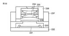
図23にこの発明を携帯電話などに使われているカメラモジュールに適用した一例の断面図を示す。センサチップ231は、ガラスエポキシなどの基板232上に接着剤で固定されている。センサチップ231のPADからワイヤ233で基板232の端子に接続されている。図示しないが、基板232では基板232の側面もしくは、底面に接続端子を引き出している。センサチップ231の上部には、赤外カット(IRcut)ガラスの2枚の光学レンズ234と、2枚のレンズ234間に絞り235を配置し、レンズバレル236上にプラスチックの樹脂で固定している。このレンズバレル236はレンズホルダ238上に固定されている。なお、センサチップ231とレンズ234との間に必要に応じてIRカットガラス板238を挿入してもよい。一般にレンズ234の枚数は、画素数が増加するにしたがって枚数が多くなっている。例えば3.2M画素では3枚レンズが多く使われている。また、センサチップ231は例えば図1の第1実施形態で説明した破線で囲んで示したCMOSイメージセンサであり、あるいは図9、10、13の実施例のイメージセンサであり、更にイメージセンサに他の機能を付加したセンサチップであってもよい。 FIG. 23 shows a sectional view of an example in which the present invention is applied to a camera module used in a mobile phone or the like. The
また、前述した各実施形態はそれぞれ、単独で実施できるばかりでなく、適宜組み合わせて実施することも可能である。さらに、前述した各実施形態には種々の段階の発明が含まれており、各実施形態において開示した複数の構成要件の適宜な組み合わせにより、種々の段階の発明を抽出することも可能である。 In addition, each of the above-described embodiments can be implemented not only independently but also in an appropriate combination. Furthermore, the above-described embodiments include inventions at various stages, and the inventions at various stages can be extracted by appropriately combining a plurality of constituent elements disclosed in the embodiments.
11,11b,11c…センサ部、12…ラインメモリ、13,13b…色相関RGB生成回路、14…信号処理部、15…システムタイミング発生回路、16…コマンドデコーダ、17…シリアルインタフェース、18,18a…レンズ、18b,18c,18c1,18c2…マイクロレンズ、111,111a…画素部、112…カラム型アナログデジタルコンバータ、130…G補間・輪郭処理部、130W…補間回路、131…第1の加算部、132…平均比率算出部、133…RGB生成部、134…エッジ処理部、135…信号合成部、136…バンドパスフィルタ、137…振幅強調部、139…輪郭信号抽出部、139S…合成回路、139W…輪郭回路、140…ボケ補正回路、141…スイッチ素子、150…シリコン基板。 DESCRIPTION OF
Claims (2)
Translated fromJapanese前記波長分離手段は、光の波長を分離するための色フィルタ層もしくは光の波長を分離しない透明フィルタ層と、前記色フィルタ層及び前記透明フィルタ層の上部に配置された1画素単位で光を集光するためのマイクロレンズとを有し、
前記画素の基本配列内において、画素数の半分に、光の波長を分離しない前記透明フィルタを有する画素が配置され、
光の波長を分離しない前記透明フィルタ層上のマイクロレンズは、前記色フィルタ層上のマイクロレンズより小さく形成され、
前記マイクロレンズのうち、面積が小さいマイクロレンズは少なくとも1層からなり、面積が大きいマイクロレンズは、前記面積が小さいマイクロレンズよりさらに、一層以上加えた層からなることを特徴とする撮像装置。2-color the optical signal by the sensor unit pixels arrangedwavelength separating meanson the front is arranged in a two-dimensional photoelectric conversion element for converting an optical signal focused on electrons by an optical lens for condensing light An image pickup apparatus including a signal processing unit that processes a signal generated by separating the wavelength component and a signal generated without wavelength separation,
The wavelength separation means includesa color filter layer for separating light wavelengths or a transparent filter layer that does not separate light wavelengths, and light in units of one pixeldisposed on the color filter layer and the transparent filter layer. A microlens for condensing,
In the basic array of pixels, a pixel having the transparent filter that does not separate the wavelength of light is arranged in half of the number of pixels,
The microlens on the transparent filter layer that does not separate the wavelength of light is formed smallerthan the microlens on the color filter layer,
Among the microlenses, the microlens having a small area is composed of at least one layer, and the microlens having a large area is composed of layers further added to the microlens having a small area .
Priority Applications (1)
| Application Number | Priority Date | Filing Date | Title |
|---|---|---|---|
| JP2008150983AJP5106256B2 (en) | 2007-06-07 | 2008-06-09 | Imaging device |
Applications Claiming Priority (3)
| Application Number | Priority Date | Filing Date | Title |
|---|---|---|---|
| JP2007151745 | 2007-06-07 | ||
| JP2007151745 | 2007-06-07 | ||
| JP2008150983AJP5106256B2 (en) | 2007-06-07 | 2008-06-09 | Imaging device |
Publications (2)
| Publication Number | Publication Date |
|---|---|
| JP2009017544A JP2009017544A (en) | 2009-01-22 |
| JP5106256B2true JP5106256B2 (en) | 2012-12-26 |
Family
ID=40095505
Family Applications (1)
| Application Number | Title | Priority Date | Filing Date |
|---|---|---|---|
| JP2008150983AExpired - Fee RelatedJP5106256B2 (en) | 2007-06-07 | 2008-06-09 | Imaging device |
Country Status (4)
| Country | Link |
|---|---|
| US (2) | US8013928B2 (en) |
| JP (1) | JP5106256B2 (en) |
| KR (1) | KR100976284B1 (en) |
| CN (1) | CN101321295B (en) |
Cited By (1)
| Publication number | Priority date | Publication date | Assignee | Title |
|---|---|---|---|---|
| US9548336B2 (en) | 2014-04-24 | 2017-01-17 | Samsung Electronics Co., Ltd. | Image sensors and electronic devices including the same |
Families Citing this family (68)
| Publication number | Priority date | Publication date | Assignee | Title |
|---|---|---|---|---|
| US6834807B2 (en)* | 2001-07-13 | 2004-12-28 | Hand Held Products, Inc. | Optical reader having a color imager |
| JP4960309B2 (en)* | 2008-06-17 | 2012-06-27 | 株式会社東芝 | Solid-state imaging device |
| WO2010036248A1 (en)* | 2008-09-24 | 2010-04-01 | Nikon Corporation | Automatic illuminant estimation and white balance adjustment based on color gamut unions |
| JP5075795B2 (en)* | 2008-11-14 | 2012-11-21 | 株式会社東芝 | Solid-state imaging device |
| US8587639B2 (en)* | 2008-12-11 | 2013-11-19 | Alcatel Lucent | Method of improved three dimensional display technique |
| JP5419749B2 (en)* | 2009-06-03 | 2014-02-19 | キヤノン株式会社 | Image processing apparatus, image processing method, and program |
| JP2010288150A (en)* | 2009-06-12 | 2010-12-24 | Toshiba Corp | Solid-state imaging device |
| JP5159715B2 (en)* | 2009-06-30 | 2013-03-13 | 株式会社東芝 | Image processing device |
| JP5059065B2 (en)* | 2009-08-07 | 2012-10-24 | シャープ株式会社 | Imaging module, imaging lens, and code reading method |
| JP5326943B2 (en)* | 2009-08-31 | 2013-10-30 | ソニー株式会社 | Image processing apparatus, image processing method, and program |
| US8248511B2 (en)* | 2009-09-30 | 2012-08-21 | Ricoh Co., Ltd. | Dual-mode extended depth-of-field imaging systems |
| JP4886016B2 (en)* | 2009-10-08 | 2012-02-29 | シャープ株式会社 | Imaging lens, imaging module, imaging lens manufacturing method, and imaging module manufacturing method |
| JP5454075B2 (en)* | 2009-10-20 | 2014-03-26 | ソニー株式会社 | Image processing apparatus, image processing method, and program |
| JP5308375B2 (en)* | 2010-02-25 | 2013-10-09 | シャープ株式会社 | Signal processing device, solid-state imaging device, electronic information device, signal processing method, control program, and recording medium |
| JP5724185B2 (en) | 2010-03-04 | 2015-05-27 | ソニー株式会社 | Image processing apparatus, image processing method, and program |
| BRPI1014549A2 (en)* | 2010-03-25 | 2016-04-05 | Fujifilm Corp | image processing method and apparatus, image processing program and storage media of this program |
| US8947584B2 (en) | 2010-12-01 | 2015-02-03 | Blackberry Limited | Apparatus, and associated method, for a camera module of electronic device |
| JP5423697B2 (en)* | 2011-02-09 | 2014-02-19 | 株式会社ニコン | Image processing apparatus, imaging apparatus, image processing program, and image processing method |
| US10046716B2 (en) | 2011-02-10 | 2018-08-14 | Denso Corporation | In-vehicle camera and vehicle control system |
| JP2012220590A (en) | 2011-04-05 | 2012-11-12 | Sharp Corp | Imaging lens and imaging module |
| JP6176028B2 (en)* | 2013-09-26 | 2017-08-09 | 株式会社デンソー | Vehicle control system, image sensor |
| US9690997B2 (en) | 2011-06-06 | 2017-06-27 | Denso Corporation | Recognition object detecting apparatus |
| EP2733944B1 (en)* | 2011-07-13 | 2016-08-03 | FUJIFILM Corporation | Image pickup apparatus and signal value correction method |
| JP5816015B2 (en) | 2011-07-15 | 2015-11-17 | 株式会社東芝 | Solid-state imaging device and camera module |
| CN102510447B (en)* | 2011-09-28 | 2016-08-10 | 上海华虹宏力半导体制造有限公司 | Imageing sensor |
| JP5901935B2 (en) | 2011-10-24 | 2016-04-13 | 株式会社東芝 | Solid-state imaging device and camera module |
| TWI514869B (en)* | 2011-12-27 | 2015-12-21 | Hon Hai Prec Ind Co Ltd | Autofocus imaging module and imaging method |
| EP2806643A1 (en)* | 2012-01-16 | 2014-11-26 | Sony Corporation | Solid-state image sensor and camera system |
| JP5743918B2 (en)* | 2012-01-31 | 2015-07-01 | 株式会社東芝 | Image processing device |
| US9568606B2 (en)* | 2012-03-29 | 2017-02-14 | Canon Kabushiki Kaisha | Imaging apparatus for distance detection using high and low sensitivity sensors with inverted positional relations |
| CN104471929B (en)* | 2012-07-06 | 2016-04-06 | 富士胶片株式会社 | Color imaging element and imaging device |
| JP6195055B2 (en)* | 2012-08-06 | 2017-09-13 | 株式会社リコー | Imaging apparatus and imaging method |
| US9143673B2 (en) | 2012-09-19 | 2015-09-22 | Google Inc. | Imaging device with a plurality of pixel arrays |
| KR101977711B1 (en)* | 2012-10-12 | 2019-05-13 | 삼성전자주식회사 | Depth sensor, image capturing method thereof and image processing system having the depth sensor |
| KR101954193B1 (en)* | 2012-11-26 | 2019-03-05 | 엘지전자 주식회사 | Array camera, electrical device, and method for operating the same |
| KR102025184B1 (en)* | 2013-07-31 | 2019-09-25 | 엘지디스플레이 주식회사 | Apparatus for converting data and display apparatus using the same |
| JP5775918B2 (en)* | 2013-09-27 | 2015-09-09 | オリンパス株式会社 | Imaging apparatus, image processing method, and image processing program |
| US9822460B2 (en) | 2014-01-21 | 2017-11-21 | Lam Research Corporation | Methods and apparatuses for electroplating and seed layer detection |
| KR102276434B1 (en) | 2014-07-03 | 2021-07-09 | 삼성전자주식회사 | Image sensor including color separation element and image pickup apparatus including the image sensor |
| US10677944B2 (en) | 2014-08-23 | 2020-06-09 | Trimble Inc. | Earthquake and displacement early warning system |
| DE102014112648A1 (en)* | 2014-08-29 | 2016-03-03 | Carl Zeiss Ag | Image pickup device and method for image acquisition |
| JP6369233B2 (en)* | 2014-09-01 | 2018-08-08 | ソニー株式会社 | Solid-state imaging device, signal processing method thereof, and electronic device |
| CN105611123B (en)* | 2015-12-18 | 2017-05-24 | 广东欧珀移动通信有限公司 | imaging method, image sensor, imaging device and electronic device |
| CN105635702B (en)* | 2015-12-18 | 2017-06-13 | 广东欧珀移动通信有限公司 | Imaging method, imaging device and electronic installation |
| CN105578072A (en)* | 2015-12-18 | 2016-05-11 | 广东欧珀移动通信有限公司 | Imaging method, imaging device and electronic device |
| CN105554485B (en)* | 2015-12-18 | 2019-04-12 | Oppo广东移动通信有限公司 | Imaging method, imaging device and electronic device |
| CN105578066B (en)* | 2015-12-18 | 2018-01-19 | 广东欧珀移动通信有限公司 | Imaging method, imaging device and electronic installation |
| CN105578080B (en)* | 2015-12-18 | 2019-02-05 | Oppo广东移动通信有限公司 | Imaging method, imaging device, and electronic device |
| CN105554419B (en)* | 2015-12-18 | 2018-04-10 | 广东欧珀移动通信有限公司 | Image sensor and terminal with same |
| CN105611122B (en)* | 2015-12-18 | 2019-03-01 | Oppo广东移动通信有限公司 | Imaging sensor and output method, phase focusing method, imaging device and terminal |
| CN105430361B (en)* | 2015-12-18 | 2018-03-20 | 广东欧珀移动通信有限公司 | Imaging method, imaging sensor, imaging device and electronic installation |
| CN105635532B (en)* | 2015-12-18 | 2017-05-24 | 广东欧珀移动通信有限公司 | imaging method, image sensor, imaging device and electronic device |
| CN105472266A (en)* | 2015-12-18 | 2016-04-06 | 广东欧珀移动通信有限公司 | High dynamic range image generation method, photographing device and terminal |
| CN105516700B (en)* | 2015-12-18 | 2018-01-19 | 广东欧珀移动通信有限公司 | Imaging method, imaging device and the electronic installation of imaging sensor |
| CN105516697B (en)* | 2015-12-18 | 2018-04-17 | 广东欧珀移动通信有限公司 | Image sensor, imaging device, mobile terminal and imaging method |
| US9735035B1 (en) | 2016-01-29 | 2017-08-15 | Lam Research Corporation | Methods and apparatuses for estimating on-wafer oxide layer reduction effectiveness via color sensing |
| JP6758859B2 (en)* | 2016-03-01 | 2020-09-23 | キヤノン株式会社 | Imaging equipment, imaging system, and image processing methods |
| EP3339821B1 (en)* | 2016-12-23 | 2025-04-16 | IMEC vzw | An imaging sensor |
| CN110326284B (en)* | 2017-03-27 | 2021-11-30 | 株式会社尼康 | Image pickup device and image pickup element |
| JP7091053B2 (en)* | 2017-10-27 | 2022-06-27 | キヤノン株式会社 | Imaging device and focus detection method |
| CN107846537B (en) | 2017-11-08 | 2019-11-26 | 维沃移动通信有限公司 | A kind of CCD camera assembly, image acquiring method and mobile terminal |
| KR102025012B1 (en)* | 2018-05-08 | 2019-09-24 | 재단법인 다차원 스마트 아이티 융합시스템 연구단 | Multi pixel micro lens pixel array and camera system for solving color mix and operating method thereof |
| US11172142B2 (en)* | 2018-09-25 | 2021-11-09 | Taiwan Semiconductor Manufacturing Co., Ltd. | Image sensor for sensing LED light with reduced flickering |
| CN113518574B (en)* | 2019-03-05 | 2024-06-18 | 奥林巴斯株式会社 | Endoscope apparatus and image processing method |
| US11640645B2 (en)* | 2019-10-25 | 2023-05-02 | Samsung Electronics Co., Ltd. | Apparatus and method of acquiring image by employing color separation lens array |
| US11128796B1 (en)* | 2020-03-03 | 2021-09-21 | Semiconductor Components Industries, Llc | High dynamic range image sensor with a neutral density filter |
| CN111385543B (en)* | 2020-03-13 | 2022-02-18 | Oppo广东移动通信有限公司 | Image sensor, camera assembly, mobile terminal and image acquisition method |
| CN112312032B (en)* | 2020-10-21 | 2022-03-25 | Tcl通讯(宁波)有限公司 | Method and device for shooting by using off-screen camera, storage medium and mobile terminal |
Family Cites Families (33)
| Publication number | Priority date | Publication date | Assignee | Title |
|---|---|---|---|---|
| JPS61252786A (en)* | 1985-05-02 | 1986-11-10 | Hitachi Ltd | solid-state imaging device |
| JP2733859B2 (en)* | 1989-09-28 | 1998-03-30 | キヤノン株式会社 | Color imaging device |
| JPH04235472A (en) | 1991-01-09 | 1992-08-24 | Canon Inc | Image pickup device |
| JP2951461B2 (en) | 1991-12-16 | 1999-09-20 | 日本電気ホームエレクトロニクス株式会社 | Color video camera |
| JPH08288482A (en)* | 1995-04-14 | 1996-11-01 | Matsushita Electron Corp | Solid-state image pickup device and its manufacture |
| JPH1126737A (en)* | 1997-06-30 | 1999-01-29 | Victor Co Of Japan Ltd | Solid-state imaging device |
| JPH11122626A (en)* | 1997-10-17 | 1999-04-30 | Nikon Corp | Image processing method and apparatus, and recording medium storing image processing program |
| GB9828166D0 (en)* | 1998-12-22 | 1999-02-17 | Eev Ltd | Imaging apparatus |
| JP2000260968A (en)* | 1999-03-04 | 2000-09-22 | Toppan Printing Co Ltd | Solid-state imaging device and method of manufacturing the same |
| JP2001245307A (en)* | 2000-03-01 | 2001-09-07 | Matsushita Electric Ind Co Ltd | Imaging device |
| EP1968054A3 (en)* | 2000-05-12 | 2012-03-07 | Konica Minolta Opto, Inc. | Optical pick-up apparatus |
| JP4210021B2 (en) | 2000-06-21 | 2009-01-14 | 富士フイルム株式会社 | Image signal processing apparatus and image signal processing method |
| JP4517493B2 (en) | 2000-10-18 | 2010-08-04 | ソニー株式会社 | Solid-state imaging device and signal processing method thereof |
| JP3942861B2 (en)* | 2001-10-23 | 2007-07-11 | 独立行政法人科学技術振興機構 | Imaging optical device |
| JP4167200B2 (en)* | 2004-04-13 | 2008-10-15 | 富士フイルム株式会社 | Signal processing apparatus, signal processing method, and digital camera |
| JP2006049636A (en) | 2004-08-05 | 2006-02-16 | Matsushita Electric Ind Co Ltd | Solid-state imaging device and manufacturing method thereof |
| JP4546797B2 (en)* | 2004-09-24 | 2010-09-15 | パナソニック株式会社 | Solid-state imaging device, manufacturing method thereof, and camera |
| WO2006064564A1 (en)* | 2004-12-16 | 2006-06-22 | Fujitsu Limited | Imaging device, imaging element, and image processing method |
| GB0501149D0 (en)* | 2005-01-20 | 2005-02-23 | Andor Technology Plc | Automatic calibration of electron multiplying CCds |
| KR101265358B1 (en)* | 2005-03-07 | 2013-05-21 | 디엑스오 랩스 | Method of controlling an action, such as a sharpness modification, using a colour digital image |
| JP2006254175A (en) | 2005-03-11 | 2006-09-21 | Matsushita Electric Ind Co Ltd | Color misregistration video signal contour correction circuit and method |
| GB2424758A (en)* | 2005-03-31 | 2006-10-04 | E2V Tech | CCD device |
| US7808063B2 (en)* | 2005-05-26 | 2010-10-05 | Micron Technology, Inc. | Structure and method for FPN reduction in imaging devices |
| JP2007047228A (en)* | 2005-08-05 | 2007-02-22 | Olympus Corp | Image forming optical apparatus and optical unit |
| JP4622790B2 (en)* | 2005-10-03 | 2011-02-02 | コニカミノルタホールディングス株式会社 | Imaging device and imaging apparatus |
| JP4782532B2 (en)* | 2005-10-14 | 2011-09-28 | 富士フイルム株式会社 | Solid-state imaging device and solid-state imaging device drive control method |
| JP5106870B2 (en) | 2006-06-14 | 2012-12-26 | 株式会社東芝 | Solid-state image sensor |
| JP2008078922A (en) | 2006-09-20 | 2008-04-03 | Toshiba Corp | Solid-state imaging device |
| JP5085140B2 (en) | 2007-01-05 | 2012-11-28 | 株式会社東芝 | Solid-state imaging device |
| JP4966035B2 (en) | 2007-01-26 | 2012-07-04 | 株式会社東芝 | Solid-state imaging device |
| JP5019204B2 (en) | 2007-01-26 | 2012-09-05 | 株式会社東芝 | Gamma correction circuit, gamma correction method and image processing apparatus |
| JP5075795B2 (en) | 2008-11-14 | 2012-11-21 | 株式会社東芝 | Solid-state imaging device |
| JP2010288150A (en) | 2009-06-12 | 2010-12-24 | Toshiba Corp | Solid-state imaging device |
- 2008
- 2008-06-04KRKR1020080052486Apatent/KR100976284B1/ennot_activeExpired - Fee Related
- 2008-06-06USUS12/134,680patent/US8013928B2/ennot_activeExpired - Fee Related
- 2008-06-06CNCN2008100986797Apatent/CN101321295B/ennot_activeExpired - Fee Related
- 2008-06-09JPJP2008150983Apatent/JP5106256B2/ennot_activeExpired - Fee Related
- 2011
- 2011-07-21USUS13/187,725patent/US8547472B2/ennot_activeExpired - Fee Related
Cited By (1)
| Publication number | Priority date | Publication date | Assignee | Title |
|---|---|---|---|---|
| US9548336B2 (en) | 2014-04-24 | 2017-01-17 | Samsung Electronics Co., Ltd. | Image sensors and electronic devices including the same |
Also Published As
| Publication number | Publication date |
|---|---|
| US20110273596A1 (en) | 2011-11-10 |
| US8013928B2 (en) | 2011-09-06 |
| KR100976284B1 (en) | 2010-08-16 |
| CN101321295A (en) | 2008-12-10 |
| US8547472B2 (en) | 2013-10-01 |
| CN101321295B (en) | 2011-07-13 |
| KR20080108019A (en) | 2008-12-11 |
| JP2009017544A (en) | 2009-01-22 |
| US20080303919A1 (en) | 2008-12-11 |
Similar Documents
| Publication | Publication Date | Title |
|---|---|---|
| JP5106256B2 (en) | Imaging device | |
| JP5713816B2 (en) | Solid-state imaging device and camera module | |
| JP5055643B2 (en) | Image pickup device and image pickup apparatus | |
| JP5075795B2 (en) | Solid-state imaging device | |
| JP4966035B2 (en) | Solid-state imaging device | |
| US8094209B2 (en) | Imaging signal processing apparatus | |
| JP4603011B2 (en) | Image capturing apparatus and operation method thereof | |
| KR20070115243A (en) | Image Imaging Apparatus, and Operation Method thereof | |
| KR20120127903A (en) | Image pickup device, digital photographing apparatus using the device, auto-focusing method, and computer-readable storage medium for performing the method | |
| WO2012026051A1 (en) | Solid-state image pickup element and image pickup apparatus | |
| JP2010288150A (en) | Solid-state imaging device | |
| JP5600814B2 (en) | Image processing apparatus and method, and imaging apparatus | |
| JP2008011532A (en) | Method and apparatus for restoring image | |
| JP2007074635A (en) | Image input device and solid-state imaging device | |
| CN104041021B (en) | Image processing device and method, and imaging device | |
| JP2006332732A (en) | Apparatus for suppressing color shift noise |
Legal Events
| Date | Code | Title | Description |
|---|---|---|---|
| A621 | Written request for application examination | Free format text:JAPANESE INTERMEDIATE CODE: A621 Effective date:20100803 | |
| A977 | Report on retrieval | Free format text:JAPANESE INTERMEDIATE CODE: A971007 Effective date:20120126 | |
| A131 | Notification of reasons for refusal | Free format text:JAPANESE INTERMEDIATE CODE: A131 Effective date:20120228 | |
| A521 | Request for written amendment filed | Free format text:JAPANESE INTERMEDIATE CODE: A523 Effective date:20120501 | |
| TRDD | Decision of grant or rejection written | ||
| A01 | Written decision to grant a patent or to grant a registration (utility model) | Free format text:JAPANESE INTERMEDIATE CODE: A01 Effective date:20120904 | |
| A01 | Written decision to grant a patent or to grant a registration (utility model) | Free format text:JAPANESE INTERMEDIATE CODE: A01 | |
| A61 | First payment of annual fees (during grant procedure) | Free format text:JAPANESE INTERMEDIATE CODE: A61 Effective date:20121002 | |
| FPAY | Renewal fee payment (event date is renewal date of database) | Free format text:PAYMENT UNTIL: 20151012 Year of fee payment:3 | |
| LAPS | Cancellation because of no payment of annual fees |