JP5101103B2 - Plasma processing method and computer storage medium - Google Patents
Plasma processing method and computer storage mediumDownload PDFInfo
- Publication number
- JP5101103B2 JP5101103B2JP2006510687AJP2006510687AJP5101103B2JP 5101103 B2JP5101103 B2JP 5101103B2JP 2006510687 AJP2006510687 AJP 2006510687AJP 2006510687 AJP2006510687 AJP 2006510687AJP 5101103 B2JP5101103 B2JP 5101103B2
- Authority
- JP
- Japan
- Prior art keywords
- plasma
- nitriding
- supply
- substrate
- microwave
- Prior art date
- Legal status (The legal status is an assumption and is not a legal conclusion. Google has not performed a legal analysis and makes no representation as to the accuracy of the status listed.)
- Expired - Fee Related
Links
Images


Classifications
- C—CHEMISTRY; METALLURGY
- C23—COATING METALLIC MATERIAL; COATING MATERIAL WITH METALLIC MATERIAL; CHEMICAL SURFACE TREATMENT; DIFFUSION TREATMENT OF METALLIC MATERIAL; COATING BY VACUUM EVAPORATION, BY SPUTTERING, BY ION IMPLANTATION OR BY CHEMICAL VAPOUR DEPOSITION, IN GENERAL; INHIBITING CORROSION OF METALLIC MATERIAL OR INCRUSTATION IN GENERAL
- C23C—COATING METALLIC MATERIAL; COATING MATERIAL WITH METALLIC MATERIAL; SURFACE TREATMENT OF METALLIC MATERIAL BY DIFFUSION INTO THE SURFACE, BY CHEMICAL CONVERSION OR SUBSTITUTION; COATING BY VACUUM EVAPORATION, BY SPUTTERING, BY ION IMPLANTATION OR BY CHEMICAL VAPOUR DEPOSITION, IN GENERAL
- C23C8/00—Solid state diffusion of only non-metal elements into metallic material surfaces; Chemical surface treatment of metallic material by reaction of the surface with a reactive gas, leaving reaction products of surface material in the coating, e.g. conversion coatings, passivation of metals
- C23C8/06—Solid state diffusion of only non-metal elements into metallic material surfaces; Chemical surface treatment of metallic material by reaction of the surface with a reactive gas, leaving reaction products of surface material in the coating, e.g. conversion coatings, passivation of metals using gases
- C23C8/36—Solid state diffusion of only non-metal elements into metallic material surfaces; Chemical surface treatment of metallic material by reaction of the surface with a reactive gas, leaving reaction products of surface material in the coating, e.g. conversion coatings, passivation of metals using gases using ionised gases, e.g. ionitriding
- H—ELECTRICITY
- H01—ELECTRIC ELEMENTS
- H01J—ELECTRIC DISCHARGE TUBES OR DISCHARGE LAMPS
- H01J37/00—Discharge tubes with provision for introducing objects or material to be exposed to the discharge, e.g. for the purpose of examination or processing thereof
- H01J37/32—Gas-filled discharge tubes
- H01J37/32009—Arrangements for generation of plasma specially adapted for examination or treatment of objects, e.g. plasma sources
- H01J37/32192—Microwave generated discharge
- H—ELECTRICITY
- H01—ELECTRIC ELEMENTS
- H01L—SEMICONDUCTOR DEVICES NOT COVERED BY CLASS H10
- H01L21/00—Processes or apparatus adapted for the manufacture or treatment of semiconductor or solid state devices or of parts thereof
- H01L21/02—Manufacture or treatment of semiconductor devices or of parts thereof
- H01L21/02104—Forming layers
- H01L21/02107—Forming insulating materials on a substrate
- H01L21/02296—Forming insulating materials on a substrate characterised by the treatment performed before or after the formation of the layer
- H01L21/02318—Forming insulating materials on a substrate characterised by the treatment performed before or after the formation of the layer post-treatment
- H01L21/02321—Forming insulating materials on a substrate characterised by the treatment performed before or after the formation of the layer post-treatment introduction of substances into an already existing insulating layer
- H01L21/02329—Forming insulating materials on a substrate characterised by the treatment performed before or after the formation of the layer post-treatment introduction of substances into an already existing insulating layer introduction of nitrogen
- H01L21/02332—Forming insulating materials on a substrate characterised by the treatment performed before or after the formation of the layer post-treatment introduction of substances into an already existing insulating layer introduction of nitrogen into an oxide layer, e.g. changing SiO to SiON
- H—ELECTRICITY
- H01—ELECTRIC ELEMENTS
- H01L—SEMICONDUCTOR DEVICES NOT COVERED BY CLASS H10
- H01L21/00—Processes or apparatus adapted for the manufacture or treatment of semiconductor or solid state devices or of parts thereof
- H01L21/02—Manufacture or treatment of semiconductor devices or of parts thereof
- H01L21/02104—Forming layers
- H01L21/02107—Forming insulating materials on a substrate
- H01L21/02296—Forming insulating materials on a substrate characterised by the treatment performed before or after the formation of the layer
- H01L21/02318—Forming insulating materials on a substrate characterised by the treatment performed before or after the formation of the layer post-treatment
- H01L21/02337—Forming insulating materials on a substrate characterised by the treatment performed before or after the formation of the layer post-treatment treatment by exposure to a gas or vapour
- H01L21/0234—Forming insulating materials on a substrate characterised by the treatment performed before or after the formation of the layer post-treatment treatment by exposure to a gas or vapour treatment by exposure to a plasma
- H—ELECTRICITY
- H01—ELECTRIC ELEMENTS
- H01L—SEMICONDUCTOR DEVICES NOT COVERED BY CLASS H10
- H01L21/00—Processes or apparatus adapted for the manufacture or treatment of semiconductor or solid state devices or of parts thereof
- H01L21/02—Manufacture or treatment of semiconductor devices or of parts thereof
- H01L21/04—Manufacture or treatment of semiconductor devices or of parts thereof the devices having potential barriers, e.g. a PN junction, depletion layer or carrier concentration layer
- H01L21/18—Manufacture or treatment of semiconductor devices or of parts thereof the devices having potential barriers, e.g. a PN junction, depletion layer or carrier concentration layer the devices having semiconductor bodies comprising elements of Group IV of the Periodic Table or AIIIBV compounds with or without impurities, e.g. doping materials
- H01L21/28—Manufacture of electrodes on semiconductor bodies using processes or apparatus not provided for in groups H01L21/20 - H01L21/268
- H01L21/28008—Making conductor-insulator-semiconductor electrodes
- H01L21/28017—Making conductor-insulator-semiconductor electrodes the insulator being formed after the semiconductor body, the semiconductor being silicon
- H01L21/28158—Making the insulator
- H01L21/28167—Making the insulator on single crystalline silicon, e.g. using a liquid, i.e. chemical oxidation
- H01L21/28202—Making the insulator on single crystalline silicon, e.g. using a liquid, i.e. chemical oxidation in a nitrogen-containing ambient, e.g. nitride deposition, growth, oxynitridation, NH3 nitridation, N2O oxidation, thermal nitridation, RTN, plasma nitridation, RPN
- H—ELECTRICITY
- H10—SEMICONDUCTOR DEVICES; ELECTRIC SOLID-STATE DEVICES NOT OTHERWISE PROVIDED FOR
- H10D—INORGANIC ELECTRIC SEMICONDUCTOR DEVICES
- H10D64/00—Electrodes of devices having potential barriers
- H10D64/60—Electrodes characterised by their materials
- H10D64/66—Electrodes having a conductor capacitively coupled to a semiconductor by an insulator, e.g. MIS electrodes
- H10D64/68—Electrodes having a conductor capacitively coupled to a semiconductor by an insulator, e.g. MIS electrodes characterised by the insulator, e.g. by the gate insulator
- H10D64/693—Electrodes having a conductor capacitively coupled to a semiconductor by an insulator, e.g. MIS electrodes characterised by the insulator, e.g. by the gate insulator the insulator comprising nitrogen, e.g. nitrides, oxynitrides or nitrogen-doped materials
- H—ELECTRICITY
- H01—ELECTRIC ELEMENTS
- H01L—SEMICONDUCTOR DEVICES NOT COVERED BY CLASS H10
- H01L21/00—Processes or apparatus adapted for the manufacture or treatment of semiconductor or solid state devices or of parts thereof
- H01L21/02—Manufacture or treatment of semiconductor devices or of parts thereof
- H01L21/02104—Forming layers
- H01L21/02107—Forming insulating materials on a substrate
- H01L21/02109—Forming insulating materials on a substrate characterised by the type of layer, e.g. type of material, porous/non-porous, pre-cursors, mixtures or laminates
- H01L21/02112—Forming insulating materials on a substrate characterised by the type of layer, e.g. type of material, porous/non-porous, pre-cursors, mixtures or laminates characterised by the material of the layer
- H01L21/02123—Forming insulating materials on a substrate characterised by the type of layer, e.g. type of material, porous/non-porous, pre-cursors, mixtures or laminates characterised by the material of the layer the material containing silicon
- H01L21/02126—Forming insulating materials on a substrate characterised by the type of layer, e.g. type of material, porous/non-porous, pre-cursors, mixtures or laminates characterised by the material of the layer the material containing silicon the material containing Si, O, and at least one of H, N, C, F, or other non-metal elements, e.g. SiOC, SiOC:H or SiONC
- H01L21/0214—Forming insulating materials on a substrate characterised by the type of layer, e.g. type of material, porous/non-porous, pre-cursors, mixtures or laminates characterised by the material of the layer the material containing silicon the material containing Si, O, and at least one of H, N, C, F, or other non-metal elements, e.g. SiOC, SiOC:H or SiONC the material being a silicon oxynitride, e.g. SiON or SiON:H
- H—ELECTRICITY
- H01—ELECTRIC ELEMENTS
- H01L—SEMICONDUCTOR DEVICES NOT COVERED BY CLASS H10
- H01L21/00—Processes or apparatus adapted for the manufacture or treatment of semiconductor or solid state devices or of parts thereof
- H01L21/02—Manufacture or treatment of semiconductor devices or of parts thereof
- H01L21/02104—Forming layers
- H01L21/02107—Forming insulating materials on a substrate
- H01L21/02225—Forming insulating materials on a substrate characterised by the process for the formation of the insulating layer
- H01L21/02227—Forming insulating materials on a substrate characterised by the process for the formation of the insulating layer formation by a process other than a deposition process
- H01L21/02252—Forming insulating materials on a substrate characterised by the process for the formation of the insulating layer formation by a process other than a deposition process formation by plasma treatment, e.g. plasma oxidation of the substrate
Landscapes
- Engineering & Computer Science (AREA)
- Chemical & Material Sciences (AREA)
- Physics & Mathematics (AREA)
- Power Engineering (AREA)
- General Physics & Mathematics (AREA)
- Microelectronics & Electronic Packaging (AREA)
- Computer Hardware Design (AREA)
- Manufacturing & Machinery (AREA)
- Condensed Matter Physics & Semiconductors (AREA)
- Chemical Kinetics & Catalysis (AREA)
- Plasma & Fusion (AREA)
- Metallurgy (AREA)
- Organic Chemistry (AREA)
- Analytical Chemistry (AREA)
- Mechanical Engineering (AREA)
- Materials Engineering (AREA)
- Crystallography & Structural Chemistry (AREA)
- General Chemical & Material Sciences (AREA)
- Formation Of Insulating Films (AREA)
- Insulated Gate Type Field-Effect Transistor (AREA)
Description
Translated fromJapanese本発明は,プラズマ処理方法及びコンピュータ記憶媒体に関するものである。 The present invention relates to a plasma processing method and a computer storage medium.
最近の半導体デバイスにおいては,動作速度を向上させるためゲート絶縁膜の厚さを薄くすることが必要である。しかしながら従前の例えばシリコン酸化膜では,膜厚を薄くするとリーク電流が増大し,かつ電極材料に含まれるホウ素(Boron)が絶縁膜を突き抜けると言う問題があり,好ましくない。そこで薄い膜厚でも所定の絶縁性を確保しつつ,しかもホウ素の拡散を抑制できる酸窒化膜を採用することが考えられている。 In recent semiconductor devices, it is necessary to reduce the thickness of the gate insulating film in order to improve the operation speed. However, the conventional silicon oxide film, for example, is not preferable because there is a problem that when the film thickness is reduced, leakage current increases and boron contained in the electrode material penetrates the insulating film. In view of this, it is considered to employ an oxynitride film capable of ensuring a predetermined insulating property even with a thin film thickness and suppressing diffusion of boron.
酸窒化膜の形成にあたっては,酸化膜を形成した後,マイクロ波を利用したプラズマ処理装置によって当該酸化膜に対してプラズマ窒化処理を行うことで酸窒化膜を形成することが提案されている(特許文献1)。かかる場合,マイクロ波は連続供給してプラズマを発生させている。 In forming an oxynitride film, it is proposed to form an oxynitride film by forming the oxide film and then subjecting the oxide film to plasma nitridation by a plasma processing apparatus using microwaves ( Patent Document 1). In such a case, microwaves are continuously supplied to generate plasma.
かかるプラズマ窒化処理による酸窒化膜の形成方法によれば,窒素分布を電極(表面)側に偏在させることができるため,熱酸化膜と同程度のフラットバンド電圧を得ることができ,かつ上記の理由により不純物の拡散を表面側で止め易い等のプラズマの利点が得られている。
プラズマ窒化処理した際には,その際のプラズマによるダメージがあるため,その後にアニール処理を行っている。従前のこの種のアニール処理は,ほぼ大気圧雰囲気で,31〜60秒間,基板を約1100℃〜1200℃で加熱するいわゆる「強いアニール処理」が採用されている。しかしながらそのような強いアニール処理を実施すると,当該アニール処理によって酸素が拡散して膜厚が増大して,誘電率が低下し,動作速度が遅くなったり,特にPMOSFETにおいて顕著であるNBTI(Negative Bias Temperature Instability:PMOSFETのゲートに負電圧を印加し,100℃程度の温度ストレスを継続して与えた場合に,経時的にソース・ドレイン間のON電流の劣化,若しくはしきい値の負方向へのシフトを発生させる現象(負電圧高温ストレス時の不安定性))特性が劣化するおそれがあった。そこで,低い電子温度のマイクロ波プラズマの利点を利用しつつ,そのようなプラズマ窒化処理を行っても,その後の強いアニール処理を不要とする技術が待たれている。
また従来は,ゲート酸化膜に窒素を導入したトランジスタの静特性(ゲートリーク電流,ソースドレインON電流)とNBTIの両者を向上させることが難しかった。When plasma nitriding is performed, there is damage due to plasma at that time, and annealing is then performed. The conventional annealing process of this type employs a so-called “strong annealing process” in which the substrate is heated at approximately 1100 ° C. to 1200 ° C. for approximately 31 to 60 seconds in an atmosphere of almost atmospheric pressure. However, when such a strong annealing process is performed, oxygen is diffused by the annealing process, the film thickness is increased, the dielectric constant is decreased, the operation speed is decreased, and NBTI (Negative Bias, which is particularly remarkable in the PMOSFET). Temperature Instability: When a negative voltage is applied to the gate of the PMOSFET and a temperature stress of about 100 ° C is continuously applied, the ON current between the source and drain deteriorates over time, or the threshold value decreases in the negative direction. There is a risk that the phenomenon that causes a shift (instability during negative voltage high temperature stress)) characteristics deteriorate. Therefore, there is a need for a technique that does not require the subsequent strong annealing process even if such a plasma nitriding process is performed while taking advantage of the microwave plasma having a low electron temperature.
Conventionally, it has been difficult to improve both the static characteristics (gate leakage current, source / drain ON current) and NBTI of a transistor in which nitrogen is introduced into the gate oxide film.
本発明は,かかる点に鑑みてなされたものであり,酸化膜形成後の基板に対して,マイクロ波によって発生させたプラズマによって窒化処理するにあたり,窒化時のダメージを抑えてその後のアニール処理を不要としたり,あるいはアニール処理を行ってもごく弱いアニール処理で済み,結果的に酸窒化膜の膜質を向上させて半導体デバイスのリーク電流の低下,動作速度の向上,並びにNBTI耐性の向上,静特性の向上を図ることを目的としている。 The present invention has been made in view of the above points, and in nitriding a substrate after forming an oxide film with plasma generated by microwaves, a subsequent annealing process is performed while suppressing damage during nitriding. Even if an annealing process is not required, an extremely weak annealing process is sufficient, and as a result, the film quality of the oxynitride film is improved to reduce the leakage current of the semiconductor device, the operation speed, the NBTI resistance, the static The purpose is to improve the characteristics.
前記目的を達成するため,本発明のプラズマ処理方法は,酸化膜形成後の基板に対して,マイクロ波によって発生させたプラズマによって窒化処理するにあたり,前記プラズマによる窒化処理の前に,減圧Arガス雰囲気内で基板を予め加熱し、次いで、Arガス雰囲気内において、前記プラズマによる窒化処理時の圧力よりも高い圧力でプラズマを着火する。そして、前記マイクロ波の供給を断続的に行ってプラズマ窒化処理を行い,前記断続的な供給におけるマイクロ波の供給ON時間を5〜100μsとし、前記断続的な供給におけるマイクロ波の供給OFF時間を5〜100μsとし、前記断続的な供給におけるマイクロ波の供給・停止の繰り返し周期を5kHz〜100kHzとし、前記断続的な供給におけるマイクロ波のパルス状波形のONデューティー比を30〜83%とし、前記窒化処理した後の,前記酸化膜中の窒素濃度を1〜20原子%に制御することで,ON電流特性とNBTI耐性の双方を、マイクロ波を連続供給して窒化処理した場合と比較して向上させることを特徴としている。例えば,いわばパルス状にマイクロ波を供給して,プラズマ窒化させるようにしている。In order to achieve the above object, the plasma processing method of the present invention uses alow pressure Ar gas before nitriding with plasma when nitriding the substrate after oxide film formation with plasma generated by microwaves.The substrate is preheated in an atmosphere, and then the plasma is ignited in an Ar gas atmosphere at a pressure higher than the pressure at the time of nitriding with the plasma. Then, thehave rows plasma nitriding performed intermittently supplyingmicrowaves, the supply ON time of the microwaves in the intermittent supply and 5~100Myuesu, supply OFF time of the microwaves in the
発明者らの知見によれば,これまでのようにマイクロ波を連続供給してプラズマ窒化処理を行っていた場合と比べると,マイクロ波の供給を断続的に行ってプラズマ窒化処理した場合には,マイクロ波の供給OFF時間においてプラズマの電子温度が下がり,酸化膜表面へのイオン衝撃を抑えることにより,酸化膜における窒素活性種の拡散速度が低下すると考えられる。その結果例えばシリコン基板と酸窒化絶縁膜との界面中に窒素が集中してその濃度が高くなることを抑えることができる。その結果,膜厚(酸化膜換算膜厚:EOT)を厚くすることなくリーク電流を抑え,しかもNBTI特性が向上した質のよい酸窒化膜が形成できる。発明者らの検証によれば,従来よりも2〜10倍,NBTI耐性が向上している。 According to the knowledge of the inventors, compared with the case where plasma nitriding is performed by continuously supplying microwaves as in the past, when the plasma nitriding is performed by intermittently supplying microwaves, It is considered that the diffusion rate of nitrogen active species in the oxide film is reduced by reducing the electron temperature of the plasma during the microwave supply OFF time and suppressing ion bombardment on the oxide film surface. As a result, for example, concentration of nitrogen in the interface between the silicon substrate and the oxynitride insulating film can be prevented from increasing. As a result, it is possible to form a high-quality oxynitride film that suppresses the leakage current without increasing the film thickness (equivalent oxide film thickness: EOT) and has improved NBTI characteristics. According to the inventors' verification, the NBTI resistance is improved by 2 to 10 times as compared with the prior art.
またさらに発明者らの検証によれば,少なくとも前記断続的な供給におけるマイクロ波の供給,停止の繰り返し周期又はマイクロ波の供給ON時間とOFF時間の比(デューティー比)を変化させることで,従来の膜中の窒素濃度を変更してもトレードオフの関係にあったMOSFETにおけるON電流特性とNBTI耐性について,その双方とも向上させられることが判明した。したがって前記したようにマイクロ波の供給を断続的に行う場合に,少なくとも繰り返し周期又はマイクロ波の供給ON時間とOFF時間の比を変化させることでON電流特性とNBTI耐性の双方を向上させ,かかる点から評価される膜質を向上させることが可能になった。 Further, according to the verification by the inventors, at least the microwave supply, the repetition cycle of the stop in the intermittent supply, or the ratio (duty ratio) of the microwave supply ON time to the OFF time is changed. It was found that both the ON current characteristics and the NBTI resistance of the MOSFET that were in a trade-off relationship could be improved even if the nitrogen concentration in the film was changed. Therefore, when the microwave supply is intermittently performed as described above, both the ON current characteristics and the NBTI resistance are improved by changing at least the repetition period or the ratio of the microwave supply ON time to the OFF time. It became possible to improve the film quality evaluated from the point.
断続的な供給は,マイクロ波の供給のON−OFFに拠ってもよいし,供給するパルス波によって変調させてもよい。
Cross-sustaining supply may be Depending on the ON-OFF of the supply of microwaves, it may be modulated by a supplied pulse wave.
また前記窒化処理した後の,酸化膜中の窒素濃度は,5〜15(原子%),好ましくは9〜13(原子%)であることが好ましい。この範囲の濃度に制御することで,リーク電流,ON電流,NBTI耐性を向上させることができる。また窒化処理の際の処理容器内の圧力は,1mTorr〜10T(0.133Pa〜1330Pa)程度が好ましい。より好ましくは,10mTorr〜1T(1.33Pa〜133.3Pa)がよい。 The nitrogen concentration in the oxide film after the nitriding treatment is preferably 5 to 15 (atomic%), preferably 9 to 13 (atomic%). By controlling the concentration within this range, leakage current, ON current, and NBTI resistance can be improved. Further, the pressure in the processing vessel at the time of nitriding is preferably about 1 mTorr to 10 T (0.133 Pa to 1330 Pa). More preferably, it is 10 mTorr to 1 T (1.33 Pa to 133.3 Pa).
このような本発明のプラズマ処理を実行する場合,次のような構成のプラズマ処理装置を用いて行われることが好ましい。すなわち,処理容器内で基板を載置する載置台と,処理容器の上方に配置され,処理空間にマイクロ波を導入してマイクロ波を発生させるため誘電体と,前記処理容器内の上方に処理ガスを供給するガス供給部と,前記ガス供給部のガス供給口よりも下方で載置台上の基板よりも上方と配置され,多数の透孔を有し,かつ少なくとも前記基板を覆う形態の誘電体板とを備えたプラズマ処理装置を用いてプラズマ窒化処理を行うと,多数の透孔を有する誘電体板によって,高エネルギーイオンが当該誘電体によって遮蔽され,窒化膜に対するダメージを軽減させることができ,プラズマ窒化処理に伴うプラズマダメージを抑えることができる。それによって,ダメージの回復を計るために実施されるその後のアニール処理を,より短時間の弱いアニール処理で済ませることができ,アニール処理による膜厚の増大を抑えることができる。 When performing such plasma processing of the present invention, it is preferable to use a plasma processing apparatus having the following configuration. That is, a mounting table on which a substrate is placed in a processing container, a dielectric that is disposed above the processing container, introduces microwaves into the processing space, and generates microwaves, and a process above the processing container. A gas supply unit configured to supply a gas; and a dielectric member configured to be disposed below the gas supply port of the gas supply unit and above the substrate on the mounting table, having a plurality of through holes, and covering at least the substrate. When plasma nitriding is performed using a plasma processing apparatus having a body plate, high-energy ions are shielded by the dielectric material by a dielectric plate having a large number of through holes, thereby reducing damage to the nitride film. And plasma damage associated with plasma nitriding can be suppressed. As a result, the subsequent annealing process performed to measure the recovery of damage can be completed by a weak annealing process for a shorter time, and an increase in film thickness due to the annealing process can be suppressed.
前記したように,プラズマ窒化処理した後は,アニール処理を行うことが必要になる場合があるが,本発明では,基板に対して減圧雰囲気でアニール処理を行うことがより好ましい。例えば,減圧容器内において,20Pa〜100000Paの減圧度で行われることがよい。また時間も1秒〜30秒間,基板を900℃〜1200℃の温度に加熱して行われる,「弱いアニール処理」でよい。 As described above, it may be necessary to perform an annealing process after the plasma nitriding process, but in the present invention, it is more preferable to perform the annealing process on the substrate in a reduced pressure atmosphere. For example, it may be performed at a reduced pressure of 20 Pa to 100000 Pa in a vacuum container. The time may also be “weak annealing” performed by heating the substrate to a temperature of 900 ° C. to 1200 ° C. for 1 second to 30 seconds.
本発明によれば,酸化膜形成後の基板に対して,マイクロ波によって発生させたプラズマによって窒化処理するにあたり,プラズマ窒化時のダメージを抑えてその後のアニール処理を不要としたり,あるいはアニール処理を行ってもごく弱いアニール処理で済ますことができる。それによって酸窒化膜の膜質を向上させて,製品化される半導体デバイスのリーク電流を抑え,動作速度の向上,並びにNBTI耐性の向上を図ることが可能である。 According to the present invention, when the substrate after the oxide film is formed by nitriding with plasma generated by microwaves, damage during plasma nitriding is suppressed, and subsequent annealing is not required, or annealing is performed. Even if it goes, it can be done with a very weak annealing treatment. Thereby, the film quality of the oxynitride film can be improved, the leakage current of the semiconductor device to be manufactured can be suppressed, the operation speed can be improved, and the NBTI resistance can be improved.
1 プラズマ処理装置
2 処理容器
3 サセプタ
5 側壁
20 透過窓
36 マイクロ波供給装置
38 パルス発振器
41 シャワープレート
51 アニール装置DESCRIPTION OF
以下,本発明の実施の形態について説明する。図1は,本実施の形態にかかるプラズマ処理方法を実施するためのプラズマ処理装置1の縦断面の様子を示しており,このプラズマ処理装置1は例えばアルミニウムからなる,上部が開口した有底円筒状の処理容器2を備えている。処理容器2は接地されている。この処理容器2の底部には,基板として例えば半導体ウエハ(以下ウエハという)Wを載置するための載置台としてのサセプタ3が設けられている。このサセプタ3は例えばアルミニウムからなり,その内部には,外部電源4からの電力の供給によって発熱するヒータ4aが設けられている。これによって,サセプタ3上のウエハWを所定温度に加熱することが可能である。 Hereinafter, embodiments of the present invention will be described. FIG. 1 shows a state of a longitudinal section of a
処理容器2の底部には,真空ポンプなどの排気装置11によって処理容器2内の雰囲気を排気するための排気管12が設けられている。また処理容器2の側壁には,処理ガス供給源からの処理ガスを供給するためのガス導入部13が設けられている。ガス導入部13には例えばガスノズルを用いることができる。本実施の形態においては,処理ガス供給源として,アルゴンガス供給源15,窒素ガス供給源16が用意され,各々バルブ15a,16a,マスフローコントローラ15b,16b,そしてバルブ15c,16cを介して,ガス導入部13に接続されている。 An
処理容器2の上部開口には,気密性を確保するためのOリングなどのシール材14を介して,たとえば誘電体の石英部材からなる透過窓20が設けられている。石英部材に代えて,他の誘電体材料,たとえばAl2O3,AlN等のセラミックスを使用してもよい。この透過窓20によって,処理容器2内に,処理空間Sが形成される。透過窓20は,平面形態が円形である。The upper opening of the
透過窓20の上方には,平面状のアンテナ部材,例えば円板状のラジアルラインスロットアンテナ30が設けられており,さらにこのラジアルラインスロットアンテナ30の上面には遅波板31が配置され,この遅波板31には,さらに遅波板31を覆う導電性のカバー32が設けられている。カバー32には冷却部が設けられ,カバー32と透過窓20を冷却するようになっている。ラジアルラインスロットアンテナ30は,導電性を有する材質,たとえばAg,Au等でメッキやコーティングされた銅の薄い円板からなり,多数のスリット33が,例えば渦巻状や同心円状に整列して形成されている。 A planar antenna member, for example, a disc-shaped radial
カバー32には同軸導波管35が接続されており,この同軸導波管35は,内側導体35aと外管35bとによって構成されている。内側導体35aは,ラジアルラインスロットアンテナ30と接続されている。内側導体35aのラジアルラインスロットアンテナ30側は円錐形を有し,ラジアルラインスロットアンテナ30に対してマイクロ波を効率よく伝播するようになっている。同軸導波管35は,マイクロ波供給装置36で発生させた,たとえば2.45GHzのマイクロ波を,矩形導波管37a,モード変換器37,同軸導波管35,遅波板31,ラジアルラインスロットアンテナ30を介して,透過窓20に伝播させる。そしてそのマイクロ波エネルギーによって透過窓20の下面に電磁界が形成されて,ガス導入部13によって処理容器2内に供給された処理ガスをプラズマ化し,サセプタ3上のウエハWに対して,プラズマ処理が行われる。そして前記マイクロ波供給装置36には,マイクロ波の供給をON−OFFするためのパルス発振器38が付設されており,このパルス発振器38の作動により,マイクロ波はパルス変調されて,断続的に供給可能である。 A
処理容器2の側壁5の上方であって,前記ガス導入部13の下方には,シャワープレート41が水平に配置されている。このシャワープレート41は,誘電体,例えば石英材によって構成され,多数の透孔42が面内均一に形成されている。このシャワープレート41によって,処理容器2内の処理空間は,上方処理空間S1,下方処理空間S2に仕切られている。このシャワープレート41によって,上方処理空間S1で発生したイオンをトラップしてラジカルのみを通過させることができる。これによりイオンダメージを抑制することができる。 A
ガス導入部13より下方の処理容器2の内壁表面には,石英ライナー42が設けられており,処理容器2内にプラズマが発生した際にスパッタリングによって処理容器2内壁表面からメタルコンタミネーションが発生するのが防止されている。 A
上記構成を有するプラズマ処理装置1は,制御装置71によって制御されている。制御装置71は,中央処理装置72,支持回路73,及び関連した制御ソフトウエアを含む記憶媒体74を有している。この制御装置71は,例えばガス導入部13からのガスの供給,停止,流量調整,ヒータ14aの温度調節,排気装置11の排気,さらにはマイクロ波供給装置36,パルス発振器38などを制御し,プラズマ処理装置1においてプラズマ処理が実施される各プロセスにおける必要な制御を行っている。 The
制御装置71の中央処理装置72は,汎用コンピュータのプロセッサを用いることができる。記憶媒体74は,例えばRAM,ROM,フレキシブルディスク,ハードディスクをはじめとした各種の形式の記憶媒体を用いることができる。また支持回路73は,各種の方法でプロセッサを支持するために中央処理装置72と接続されている。 The
プラズマ処理装置1は以上の構成を有しており,例えば熱酸化処理,あるいはプラズマ酸化処理によって表面にシリコン酸化膜が形成されたウエハWに対して,プラズマ窒化処理する際には,処理容器2内のサセプタ3上にウエハWを載置し,ガス導入部13から所定の処理ガス,例えばAr/N2の混合ガスを,例えば1000/40sccmの流量で処理容器2内に供給しつつ,排気管12から排気することで,処理空間S内を所定の圧力,例えば1.3Pa〜133.3Pa,好ましくは6.7Pa〜126.6Paにする。ここでは6.7Paにする。そしてマイクロ波供給装置36によって高周波のマイクロ波を発生させて,パルス発振器38による変調によってマイクロ波の供給を断続的に行い,同軸導波管35,遅波板31を介し,ラジアルラインスロットアンテナ30へマイクロ波を均一に伝播させる。このときのマイクロ波のパワーは,平均800W,繰り返し周期は,ON:50μs,OFF:50μsである。それによってラジアルラインスロットアンテナ30のスリット33から透過窓20に対して電磁波の供給が断続的に行われる。The
これによって,透過窓20の下面に電界が形成され,上方処理空間S1において,前記処理ガスがプラズマ化される。そして窒素ラジカルがシャワープレート41の透孔42を通過して,ウエハWの表面に均一に供給され,酸化膜に対して窒化処理が行われる。この際のプラズマの密度は,1×1010〜5×10¹²/cm3であり,プラズマの電子温度は0.1〜1eVに低く制御されるので,高密度でイオンのエネルギーを低くでき,低ダメージのプラズマ処理が可能である。As a result, an electric field is formed on the lower surface of the
このときマイクロ波の供給は断続的に行われるので,平均的窒素イオン照射エネルギーが低下すると共に,供給OFF時間においてウエハWの表面温度が下がり,酸化膜における窒化種の拡散速度が低下し,ダメージの少ないプラズマ窒化処理が行われる。しかも前記プラズマ処理装置1では,シャワープレート41を介してプラズマ窒化処理が行われるので,高エネルギーイオンの直射がシャワープレート41によって遮蔽されるので,かかる点からも,ウエハWの酸化膜に対してダメージの少ないプラズマ窒化処理が行われる。 At this time, since the microwave supply is intermittently performed, the average nitrogen ion irradiation energy decreases, the surface temperature of the wafer W decreases during the supply OFF time, the diffusion rate of nitride species in the oxide film decreases, and damage occurs. A plasma nitriding process with a small amount is performed. Moreover, in the
マイクロ波の断続的な供給ON時間は,1周期あたり,5〜100μsであることが好ましい。またマイクロ波の供給,停止の繰り返し周期は,5kHz〜100kHzであることが好ましい。また断続的な供給におけるマイクロ波の供給ON時間とOFF時間の比は,0.10〜5:1,すなわち,供給されるマイクロ波をパルス状波形とみたとき,ONデューティー比は,9〜90%であることが好ましい。より好ましくは30〜83%,さらに好ましくは50%である。 The intermittent supply ON time of the microwave is preferably 5 to 100 μs per cycle. Further, the repetition cycle of the supply and stop of the microwave is preferably 5 kHz to 100 kHz. Further, the ratio of the microwave ON time and the OFF time in intermittent supply is 0.10 to 5: 1, that is, when the supplied microwave is regarded as a pulse waveform, the ON duty ratio is 9 to 90. % Is preferred. More preferably, it is 30 to 83%, and still more preferably 50%.
そのようにしてプラズマ窒化処理されたウエハWは,次にアニール処理されてもよい。アニール処理は,種々のアニール装置が使用できるが,例えば図2に示したランプアニール方式のアニール装置51を使用することができる。 The wafer W thus plasma-nitrided may then be annealed. For the annealing treatment, various annealing apparatuses can be used. For example, a lamp annealing
このアニール装置51は,処理容器52の内部上方に,透明な石英板53が水平に渡され,蓋部54と石英板53との間の空間には,加熱源として例えばランプ54が配置されている。処理容器52の底部は,真空排気手段(図示せず)に通ずる排気口55が形成されている。処理容器2の側壁における石英板53の下方には,ガス供給口56が設けられている。ウエハWは,処理容器2の底部に設置された支持ピン57上に載置される。 In this
かかるアニール装置51において,プラズマ窒化処理後のウエハWに対して,アニール処理が行われる。処理条件としては,例えばガス供給口56からN2/O2の混合ガスが供給され,また処理容器2内は例えば133Pa(1Torr)程度に減圧され,ウエハWは1000℃程度に加熱される。なお処理ガスとしては,その他に,例えば少なくとも酸素を含むガスであり,酸素分圧を下げるためたとえば窒素ガスで希釈して用いるのがよい。さらにはアンモニア,水素を添加して使用できる。このような加熱条件の下,ウエハWは,例えば1〜30秒,より好ましくは5〜10秒の,弱いアニール処理に付される。従来の窒化処理後のアニール処理と比べると,このような減圧雰囲気における短時間のアニール処理が好ましい。これによって酸窒化膜の膜厚をさほど増大させることなく,酸窒化膜の膜質,すなわちNBTI耐性,ON電流特性をさらに向上させると共に,プラズマ処理後の酸窒化膜中及び界面のダメージを回復させることができる。In the
上記実施例にかかるプラズマ処理方法によって,例えばP−MOSFETのゲート絶縁膜を形成した際の効果について説明する。図3は,P−MOSFET61の構造を概略的に示しており,N型半導体基板62にP型半導体63,64が各々形成され,各々ドレイン電極67,ソース電極68が引き出される。そしてその間にゲート絶縁膜65が形成され,その上にゲート電極66が形成され,さらにゲート引き出し電極69が形成されている。そしてこのゲート絶縁膜65に,前記したプラズマ窒化処理された酸窒化膜が採用されている。なおN−MOSFETはN型半導体基板62とP型半導体63,64を逆に形成することで構成される。 The effect when, for example, a gate insulating film of a P-MOSFET is formed by the plasma processing method according to the above embodiment will be described. FIG. 3 schematically shows the structure of the P-
本実施の形態によってプラズマ窒化された酸窒化膜をゲート絶縁膜65に採用した場合,N型半導体基板62とのゲート絶縁膜65における界面側には,窒素の濃度が従来のプラズマ窒化処理された酸窒化膜よりも抑えて制御されおり,その結果NBTI耐性が向上している。次にその他の特性と共にこれをより詳述する。 When the oxynitride film plasma-nitrided according to the present embodiment is used for the
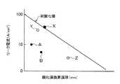
図4は,酸化膜換算膜厚とリーク電流との関係において,酸化膜(X)に対して「従来のプラズマ窒化処理」(Y)と「従来のプラズマ窒化処理+従前のアニール処理」(Z)を施した場合と,本実施の形態による処理,すなわち「マイクロ波の断続供給によるプラズマ窒化処理」(A)と,「マイクロ波の断続供給によるプラズマ窒化処理+本発明のアニール処理(弱いアニール処理)」(B)を施した場合とを各々示している。 FIG. 4 shows the relationship between the oxide equivalent film thickness and the leakage current with respect to the oxide film (X) “conventional plasma nitridation process” (Y) and “conventional plasma nitridation process + previous annealing process” (Z ) And the processing according to the present embodiment, that is, “plasma nitriding by intermittent supply of microwaves” (A) and “plasma nitriding by intermittent supply of microwaves + annealing of the present invention (weak annealing) (Process) ”(B) is shown.
図4に示したN−MOSFETよれば,「従来のプラズマ窒化処理」(Y)よりも,実施の形態にかかる「マイクロ波の断続供給によるプラズマ窒化処理」(A)の方が,ゲート絶縁膜間のリーク電流のさらなる低減が図られており,しかも膜厚が薄い。そしてこれにさらにアニール処理を施した場合,「従来のプラズマ窒化処理+従前のアニール処理」(Z)では,リーク電流は確かに低減されるが,膜厚がかなり増大し,高速動作性が劣化してしまう。これに対し,「マイクロ波の断続供給によるプラズマ窒化処理+本発明のアニール処理(弱いアニール処理)」(B)では,リーク電流の値自体は,従来型よりも多少劣るが,膜厚の増大は僅かであり,高速動作性が確保されている。 According to the N-MOSFET shown in FIG. 4, the “plasma nitriding treatment by intermittent microwave supply” (A) according to the embodiment is more suitable than the “conventional plasma nitriding treatment” (Y). The leakage current is further reduced, and the film thickness is thin. When this is further annealed, the leak current is certainly reduced in the “conventional plasma nitriding process + conventional annealing process” (Z), but the film thickness increases considerably and high-speed operability deteriorates. Resulting in. On the other hand, in “plasma nitriding treatment by intermittent supply of microwaves + annealing treatment of the present invention (weak annealing treatment)” (B), the leakage current value is somewhat inferior to that of the conventional type, but the film thickness is increased. Are few, and high-speed operation is ensured.
次に酸化膜換算膜厚とソース−ドレイン間のN−MOSFETのON電流特性について調べると,図5に示したように,実施の形態の方が,「マイクロ波の断続供給によるプラズマ窒化処理」(A)と,「マイクロ波の断続供給によるプラズマ窒化処理+本発明のアニール処理(弱いアニール処理)」(B)のいずれの場合も,従来より高いON電流値が得られている。 Next, when the equivalent oxide thickness and the ON-current characteristics of the N-MOSFET between the source and the drain are examined, as shown in FIG. 5, the embodiment is “plasma nitriding by intermittent microwave supply”. In both cases (A) and “plasma nitridation by intermittent supply of microwaves + annealing of the present invention (weak annealing)” (B), a higher ON current value is obtained than in the prior art.
なお図5において,(C)は,プラズマ処理装置1において,シャワープレート41を外した図6のプラズマ処理装置81を用いて,同様なマイクロ波の断続供給によるプラズマ窒化処理した場合を示している。すなわち,図6のプラズマ処理装置81は,図1に示したプラズマ処理装置81におけるシャワープレート41を取り外した構成を有しており,その他の構成は,図1のプラズマ処理装置1と同一の構成を有するものである。 In FIG. 5, (C) shows a case where the plasma nitriding process by the intermittent supply of microwaves is performed in the
図5に示した結果をみると,プラズマ窒化処理する際,図1に示したシャワープレート41を有するプラズマ処理装置1によってプラズマ窒化処理した方が,さらに高いMOSFETのON電流値が得られることが判明した。これは,シャワープレート41による入射イオン量の低減効果と,マイクロ波の断続供給による電子温度低下に伴う,さらなる入射イオンエネルギーの低下効果とが相乗して,さらに良好な結果が得られたものと考える。 When the results shown in FIG. 5 are seen, when plasma nitriding is performed, the plasma nitriding treatment using the
次にN−MOSFETのON電流とNBTI(負電圧高温ストレス印加時の信頼性:例えばしきい値電圧シフト量,ON電流値が許容範囲を超えるまでの寿命若しくはそれらのシフト量,劣化度合いが指標となっている)耐性について調べた。図7に示したように,実施の形態にかかるプラズマ窒化処理の方が,はるかに高いNBTI耐性が得られている。また(D)は,前記したプラズマ窒化処理後に行うアニール処理について,「弱いアニール処理」に代えて,従来のこの種の「強いアニール処理」を施した場合を示しているが,本発明にかかるプラズマ窒化処理を行えば,たとえその後に従前の「強いアニール処理」を行っても,依然として従来よりも高いNBTI耐性を示している。 Next, N-MOSFET ON current and NBTI (reliability when negative voltage high temperature stress is applied: for example, threshold voltage shift amount, life until ON current value exceeds allowable range, shift amount thereof, and deterioration degree are indicators. The resistance was examined. As shown in FIG. 7, the plasma nitriding process according to the embodiment has much higher NBTI resistance. Further, (D) shows the case where the conventional “strong annealing process” of this kind is performed instead of the “weak annealing process” for the annealing process performed after the plasma nitriding process. If the plasma nitriding process is performed, even if the subsequent “strong annealing process” is performed, the NBTI resistance is still higher than the conventional one.
次に前出プラズマ処理装置1を使用して,各種のプラズマ条件を変化させてP−MOSFETのゲート絶縁膜を構成する酸化膜に対してプラズマ窒化処理を行い,それによって形成された酸窒化膜を有するPMOSのON電流特性を横軸に,NBTI耐性を縦軸にとった結果を図8に示した。このときのプラズマ窒化条件は,次の通りである。 Next, plasma nitriding treatment is performed on the oxide film constituting the gate insulating film of the P-MOSFET by changing various plasma conditions using the
ベース酸化膜の膜厚が1.0nm,処理容器内の圧力は,50mTorr(6.65Pa),パワーは,1500Wである。またプラズマ窒化処理する際のガスは,アルゴンガス/窒素ガスの流量比が,1000sccm/40sccmである。プラズマ窒化処理時間は,5,10,20,40秒として,そのときのゲート酸化膜中の窒素濃度が,各々5原子%,9原子%,11原子%,15原子%となる。 The thickness of the base oxide film is 1.0 nm, the pressure in the processing container is 50 mTorr (6.65 Pa), and the power is 1500 W. The gas used for the plasma nitriding treatment has an argon gas / nitrogen gas flow ratio of 1000 sccm / 40 sccm. The plasma nitriding time is 5, 10, 20, and 40 seconds, and the nitrogen concentrations in the gate oxide film at that time are 5 atomic%, 9 atomic%, 11 atomic%, and 15 atomic%, respectively.
図8において,各パルス条件は,
パルス条件1は,ON時間/OFF時間が50μS/50μS(ONデューティー50%,繰返し周期10kHz),
パルス条件2は,ON時間/OFF時間が50μS/10μS(ONデューティー83%,繰返し周期17kHz),
パルス条件3は,ON時間/OFF時間が10μS/10μS(ONデューティー50%,繰返し周期50kHz),
パルス条件4は,ON時間/OFF時間が200μS/500μS(ONデューティー29%,繰返し周期1kHz)
である。
なお図中,CWは,連続波の場合を示している。In FIG. 8, each pulse condition is
Pulse condition 4 is ON time / OFF time 200μS / 500μS (ON duty 29%, repetition period 1kHz)
It is.
In the figure, CW indicates the case of a continuous wave.
これによれば,パルス条件4の場合は連続波と変わりがないが,パルス条件3からパルス条件1に変えるにつれて,PMOSのON電流特性とNBTI耐性が共に向上することが確認できた。すなわち従来の連続波では,ON電流特性とNBTI耐性とがトレードオフの関係にあり,膜中の窒素濃度を変更していずれか一方を向上させると,他方が低下していたが,本実施例のように,ON時間/OFF時間(デューティー比と繰返し周期)を変更することによって,ON電流特性とNBTI耐性の双方を向上させることが可能であることが確認できた。すなわち,膜中の窒素濃度が5原子%のときには,NBTI耐性の方がより高く向上し,この傾向は窒素濃度が9原子%のときにもほぼ同様な傾向である。そして窒素濃度が11原子%のときには,NBTI耐性,ON電流特性の双方ともほぼ同程度に向上させることができ,窒素濃度が15原子%のときには,ON電流特性の方をより向上させることができる。窒素濃度はこの範囲に限られず,好ましい範囲は,1〜20原子%,より好ましくは5〜15原子%,さらに好ましくは9〜13原子%がよい。いずれにしても,ON電流特性とNBTI耐性の双方を従来よりも向上させることができる。 According to this, although the pulse condition 4 is not different from the continuous wave, it was confirmed that as the
さらにプラズマ処理装置1を用いたプラズマ窒化処理の工程の一例を説明する。 Further, an example of a plasma nitriding process using the
まず表面に酸化膜が形成されたウエハWを処理容器2内に搬入し,サセプタ上にウエハWを載置する。そして処理容器2内にArガスを,例えば2000sccmの流量で供給しつつ,排気装置11によって処理容器2内の雰囲気を排気し,処理容器2内の圧力を126.66Paの減圧度に維持する。このときヒータ4aによってウエハWを例えば400℃に加熱する。このようにウエハWを事前に十分に加熱し,また処理容器2内を減圧することで,ウエハWに付着していた水分を効果的に除去でき,またArガスを供給しつつ処理容器2内を排気しているので,前記ウエハWから除去した水分や,処理容器2内の残留雰囲気を効果的にパージすることができる。これによってプラズマ窒化処理の際にN原子を基板に均一に,かつ効果的に導入できる。このようないわばプリヒート工程は,例えば70秒間行われる。 First, a wafer W having an oxide film formed on the surface is carried into the
次いでプラズマ着火工程が行われる。このとき処理容器2内には,例えば2000sccmの流量でArガスが供給され続け,処理容器2内の圧力は,126.66Paの減圧度に維持される。このように本来のプラズマ窒化処理時の圧力よりも高く処理容器2内の圧力を設定することで,いわゆるプラズマ着火がしやすい。なおプラズマ着火の際のマイクロ波供給装置36の出力は2000Wであり,またこのようなプラズマ着火工程は,例えば5秒間行われる。 Next, a plasma ignition process is performed. At this time, Ar gas is continuously supplied into the
次いでプラズマ窒化処理を安定にするため,処理容器2内をさらに減圧してその圧力を6.7Paにする。このときArガスの供給流量は1000sccmに落とされ,またマイクロ波供給装置36の出力も1500Wに落とされ,処理容器2内の圧力,マイクロ波供給装置36の出力とも,プラズマ窒化処理時の圧力,出力に設定される。このようないわば準備,調整工程は例えば5秒間行われる。 Next, in order to stabilize the plasma nitriding treatment, the inside of the
次いで,処理容器2内の圧力が6.7Pa,マイクロ波供給装置36の出力が1500W,Arガスの供給流量が1000sccmに各々維持されたまま,処理容器2内に窒素ガスが,たとえば40sccmの流量で供給され,ウエハWの酸化膜に対してプラズマ窒化処理がなされる。このプラズマ窒化処理の時間は,例えば5〜40秒間である。 Next, while maintaining the pressure in the
所定のプラズマ窒化処理が終了すると,マイクロ波供給装置36を停止し,プラズマを消失させる(いわゆるプラズマOFF)。このとき窒素ガスは40sccm,Arガスは1000sccmの供給流量が維持され,処理容器2内の圧力も6.7Paに維持される。このようなプラズマ消失の工程が例えば3秒間行われる。 When the predetermined plasma nitriding process is completed, the
次いで窒素ガス,Arガスの供給が停止され,例えばプラズマ処理装置1と接続されているロードロック室のような予備室と同じ圧力まで,処理容器内の圧力が高められた後,ウエハWは処理容器2から搬出される。 Next, the supply of nitrogen gas and Ar gas is stopped, and the wafer W is processed after the pressure in the processing chamber is increased to the same pressure as that of a spare chamber such as a load lock chamber connected to the
このような工程でプラズマ窒化処理を行うことで,低プラズマダメージで窒素を均一に酸化膜表面側に導入することができ,NBTI耐性,ON電流特性を向上させることができる。 By performing plasma nitriding in such a process, nitrogen can be uniformly introduced into the oxide film surface side with low plasma damage, and NBTI resistance and ON current characteristics can be improved.
以上のプラズマ処理にあたっては,プラズマ源として平面アンテナを用いたマイクロ波プラズマを使用したが,その他のプラズマ源として平行平板型(容量型)プラズマ,誘導結合型プラズマ(ICP),ECRプラズマ,表面波プラズマ,マグネトロン型プラズマ等が適用可能である。 In the above plasma processing, microwave plasma using a planar antenna was used as a plasma source, but parallel plate type (capacitive type) plasma, inductively coupled plasma (ICP), ECR plasma, surface wave were used as other plasma sources. Plasma, magnetron type plasma, etc. are applicable.
本発明は,リーク電流を増大させることなく半導体デバイスの絶縁膜を薄くすることができ,特に動作速度が高速の半導体デバイスの製造に有用である。 INDUSTRIAL APPLICABILITY The present invention can reduce the insulating film of a semiconductor device without increasing leakage current, and is particularly useful for manufacturing a semiconductor device having a high operating speed.
Claims (8)
Translated fromJapanese次いで、Arガス雰囲気内において、前記プラズマによる窒化処理時の圧力よりも高い圧力でプラズマを着火し、
前記プラズマによる窒化処理は,マイクロ波の供給を断続的に行って発生させたプラズマによって行い,
前記断続的な供給におけるマイクロ波の供給ON時間を5〜100μsとし、
前記断続的な供給におけるマイクロ波の供給OFF時間を5〜100μsとし、
前記断続的な供給におけるマイクロ波の供給・停止の繰り返し周期を5kHz〜100kHzとし、
前記断続的な供給におけるマイクロ波のパルス状波形のONデューティー比を30〜83%とし、
前記窒化処理した後の,酸化膜中の窒素濃度を1〜20原子%に制御することで,当該窒化処理した後の、酸化膜のON電流特性とNBTI耐性の双方を、マイクロ波を連続供給して窒化処理した場合と比較して向上させる。A plasma processing method for nitriding a substrate after oxide film formation with plasma generated by microwaves,wherein the substrate is preheated in a reduced pressure Ar gas atmosphere before nitriding with the plasma,
Next, in an Ar gas atmosphere, the plasma is ignited at a pressure higher than the pressure at the time of nitriding with the plasma,
The nitriding treatment by the plasma is performed by plasma generated by intermittently supplying a microwave,
The microwave supply ON time in the intermittent supply is set to 5 to 100 μs,
The microwave supply OFF time in the intermittent supply is set to 5 to 100 μs,
The repetition cycle of microwave supply / stop in the intermittent supply is 5 kHz to 100 kHz,
The ON duty ratio of the pulse waveform of the microwave in the intermittent supply is 30 to 83%,
By controlling the nitrogen concentration in the oxide film after the nitriding process to 1 to 20 atomic%, both the ON current characteristics and the NBTI resistance of the oxide film after the nitriding processare continuously supplied with microwaves. Thus, it is improved ascompared with the case of nitriding treatment .
前記酸化膜中の窒素濃度は5〜15原子%である。The nitrogen concentration in the oxide film is 5 to 15 atomic%.
前記プラズマ窒化処理は,プラズマ処理装置を用いて行われ,The plasma nitriding process is performed using a plasma processing apparatus,
前記プラズマ処理装置は,The plasma processing apparatus includes:
処理容器内で基板を載置する載置台と,A mounting table for mounting a substrate in a processing container;
処理容器の上方に配置され,処理空間にマイクロ波を導入してマイクロ波を発生させるため誘電体と,A dielectric material disposed above the processing vessel for introducing microwaves into the processing space to generate microwaves;
前記処理容器内の上方に処理ガスを供給するガス供給部と,A gas supply unit for supplying a processing gas to the upper side of the processing container;
前記ガス供給部のガス供給口よりも下方で載置台上の基板よりも上方に配置され,多数の透孔を有し,かつ少なくとも前記基板を覆う形態の誘電体板とを備えている。A dielectric plate disposed below the gas supply port of the gas supply unit and above the substrate on the mounting table, having a plurality of through holes and covering at least the substrate;
前記プラズマ窒化処理の後,さらに前記基板に対して減圧雰囲気でアニール処理を行う工程を有する。After the plasma nitriding process, the substrate further includes a step of annealing the substrate in a reduced pressure atmosphere.
前記アニール処理は,減圧容器内において,20〜100000Paの減圧度で行われる。The annealing treatment is performed at a reduced pressure of 20 to 100,000 Pa in a reduced pressure container.
前記アニール処理は,1秒〜30秒間,基板を900℃〜1200℃の温度に加熱して行われる。The annealing process is performed by heating the substrate to a temperature of 900 ° C. to 1200 ° C. for 1 second to 30 seconds.
前記アニール処理は,少なくとも酸素を含むガスを減圧容器内に導入し,この減圧容器内において行われる。The annealing process is performed in this decompression vessel by introducing a gas containing at least oxygen into the decompression vessel.
前記プラズマ処理方法は,マイクロ波の断続的な供給によって発生させたプラズマにより,酸化膜形成後の基板に対して窒化処理するプラズマ処理方法であって,前記プラズマによる窒化処理の前に,減圧Arガス雰囲気内で基板を予め加熱し、The plasma processing method is a plasma processing method for nitriding the substrate after the oxide film is formed by plasma generated by intermittent supply of microwaves, and the reduced pressure Ar is applied before the nitriding processing by the plasma. Pre-heating the substrate in a gas atmosphere,
次いで、Arガス雰囲気内において、前記プラズマによる窒化処理時の圧力よりも高い圧力でプラズマを着火し、Next, in an Ar gas atmosphere, the plasma is ignited at a pressure higher than the pressure at the time of nitriding with the plasma,
前記プラズマによる窒化処理において,In the nitriding treatment by the plasma,
前記断続的な供給におけるマイクロ波の供給ON時間を5〜100μsとし、The microwave supply ON time in the intermittent supply is set to 5 to 100 μs,
前記断続的な供給におけるマイクロ波の供給OFF時間を5〜100μsとし、The microwave supply OFF time in the intermittent supply is set to 5 to 100 μs,
前記断続的な供給におけるマイクロ波の供給・停止の繰り返し周期を5kHz〜100kHzとし、The repetition cycle of microwave supply / stop in the intermittent supply is 5 kHz to 100 kHz,
前記断続的な供給におけるマイクロ波のパルス状波形のONデューティー比を30〜83%とし、The ON duty ratio of the pulse waveform of the microwave in the intermittent supply is 30 to 83%,
前記窒化処理した後の,前記酸化膜中の窒素濃度を1〜20原子%に制御することで,ON電流特性とNBTI耐性の双方を、マイクロ波を連続供給して窒化処理した場合と比較して向上させる。By controlling the nitrogen concentration in the oxide film after the nitriding treatment to 1 to 20 atomic%, both the ON current characteristics and the NBTI resistance are compared with the case where the nitriding treatment is performed by continuously supplying microwaves. Improve.
Priority Applications (1)
| Application Number | Priority Date | Filing Date | Title |
|---|---|---|---|
| JP2006510687AJP5101103B2 (en) | 2004-03-03 | 2005-03-02 | Plasma processing method and computer storage medium |
Applications Claiming Priority (6)
| Application Number | Priority Date | Filing Date | Title |
|---|---|---|---|
| JP2004058945 | 2004-03-03 | ||
| JP2004058945 | 2004-03-03 | ||
| JP2004268236 | 2004-09-15 | ||
| JP2004268236 | 2004-09-15 | ||
| JP2006510687AJP5101103B2 (en) | 2004-03-03 | 2005-03-02 | Plasma processing method and computer storage medium |
| PCT/JP2005/003488WO2005086215A1 (en) | 2004-03-03 | 2005-03-02 | Plasma processing method and computer storing medium |
Publications (2)
| Publication Number | Publication Date |
|---|---|
| JPWO2005086215A1 JPWO2005086215A1 (en) | 2008-01-24 |
| JP5101103B2true JP5101103B2 (en) | 2012-12-19 |
Family
ID=34921660
Family Applications (1)
| Application Number | Title | Priority Date | Filing Date |
|---|---|---|---|
| JP2006510687AExpired - Fee RelatedJP5101103B2 (en) | 2004-03-03 | 2005-03-02 | Plasma processing method and computer storage medium |
Country Status (7)
| Country | Link |
|---|---|
| US (3) | US7723241B2 (en) |
| EP (1) | EP1722406A1 (en) |
| JP (1) | JP5101103B2 (en) |
| KR (2) | KR100956467B1 (en) |
| CN (2) | CN1926670B (en) |
| TW (1) | TW200540992A (en) |
| WO (1) | WO2005086215A1 (en) |
Families Citing this family (13)
| Publication number | Priority date | Publication date | Assignee | Title |
|---|---|---|---|---|
| TW200511430A (en)* | 2003-05-29 | 2005-03-16 | Tokyo Electron Ltd | Plasma processing apparatus and plasma processing method |
| KR100956467B1 (en) | 2004-03-03 | 2010-05-07 | 도쿄엘렉트론가부시키가이샤 | Plasma Treatment Method |
| JPWO2008081724A1 (en)* | 2006-12-28 | 2010-04-30 | 東京エレクトロン株式会社 | Method for forming insulating film and method for manufacturing semiconductor device |
| KR20090094033A (en)* | 2006-12-28 | 2009-09-02 | 도쿄엘렉트론가부시키가이샤 | Method for forming insulating film and method for manufacturing semiconductor device |
| CN101681836B (en)* | 2007-05-29 | 2011-11-16 | 东京毅力科创株式会社 | Method for pretreating inner space of chamber in plasma nitridation, plasma processing method and plasma processing apparatus |
| JP5520455B2 (en)* | 2008-06-11 | 2014-06-11 | 東京エレクトロン株式会社 | Plasma processing equipment |
| JP5357486B2 (en)* | 2008-09-30 | 2013-12-04 | 東京エレクトロン株式会社 | Plasma processing equipment |
| JP5490087B2 (en)* | 2011-12-28 | 2014-05-14 | 東京エレクトロン株式会社 | Microwave heat treatment apparatus and treatment method |
| KR101851199B1 (en) | 2011-12-28 | 2018-04-25 | 삼성전자주식회사 | Semiconductor device having a nitride gate insulating layer and method of fabricating the same |
| CN106159036A (en)* | 2015-04-13 | 2016-11-23 | 中兴通讯股份有限公司 | A kind of preparation method of silicon based opto-electronics subsystem |
| JP2019009305A (en)* | 2017-06-26 | 2019-01-17 | 東京エレクトロン株式会社 | Plasma processing apparatus |
| CN112864007B (en)* | 2019-11-28 | 2022-04-12 | 长鑫存储技术有限公司 | Method for forming semiconductor structure |
| TWI793744B (en)* | 2020-09-09 | 2023-02-21 | 日商國際電氣股份有限公司 | Manufacturing method and program of substrate processing apparatus and semiconductor device |
Citations (8)
| Publication number | Priority date | Publication date | Assignee | Title |
|---|---|---|---|---|
| JPH02141576A (en)* | 1988-11-18 | 1990-05-30 | Sumitomo Metal Ind Ltd | plasma process equipment |
| JPH08288271A (en)* | 1995-04-18 | 1996-11-01 | Sony Corp | Method and apparatus for film deposition |
| JP2002222941A (en)* | 2001-01-24 | 2002-08-09 | Sony Corp | MIS type semiconductor device and method of manufacturing the same |
| JP2003078132A (en)* | 2001-08-31 | 2003-03-14 | Toshiba Corp | Method for manufacturing semiconductor device |
| JP2003077915A (en)* | 2001-09-04 | 2003-03-14 | Matsushita Electric Ind Co Ltd | Method and apparatus for forming insulating film |
| JP2003282565A (en)* | 2002-01-18 | 2003-10-03 | Arieesu Gijutsu Kenkyu Kk | Film deposition method, film deposition apparatus, and semiconductor device |
| JP2004022902A (en)* | 2002-06-18 | 2004-01-22 | Fujitsu Ltd | Method for manufacturing semiconductor device |
| JP2004048001A (en)* | 2002-07-01 | 2004-02-12 | Internatl Business Mach Corp <Ibm> | Method of forming silicon nitride oxide gate insulating film |
Family Cites Families (12)
| Publication number | Priority date | Publication date | Assignee | Title |
|---|---|---|---|---|
| KR100537679B1 (en)* | 1996-07-12 | 2006-04-06 | 동경 엘렉트론 주식회사 | Film deposition apparatus and film formation method |
| US6143081A (en)* | 1996-07-12 | 2000-11-07 | Tokyo Electron Limited | Film forming apparatus and method, and film modifying apparatus and method |
| KR200156080Y1 (en) | 1996-08-22 | 1999-09-01 | 유창근 | Control valve of chair oil-pressure cylinder |
| KR100745495B1 (en)* | 1999-03-10 | 2007-08-03 | 동경 엘렉트론 주식회사 | Semiconductor manufacturing method and semiconductor manufacturing apparatus |
| JP2002208593A (en) | 2001-01-11 | 2002-07-26 | Tokyo Electron Ltd | Method for formation of silicon oxynitride film |
| TWI225668B (en)* | 2002-05-13 | 2004-12-21 | Tokyo Electron Ltd | Substrate processing method |
| WO2003098678A1 (en) | 2002-05-16 | 2003-11-27 | Tokyo Electron Limited | Method of treating substrate |
| US7179754B2 (en)* | 2003-05-28 | 2007-02-20 | Applied Materials, Inc. | Method and apparatus for plasma nitridation of gate dielectrics using amplitude modulated radio-frequency energy |
| KR100956467B1 (en)* | 2004-03-03 | 2010-05-07 | 도쿄엘렉트론가부시키가이샤 | Plasma Treatment Method |
| US7163877B2 (en)* | 2004-08-18 | 2007-01-16 | Tokyo Electron Limited | Method and system for modifying a gate dielectric stack containing a high-k layer using plasma processing |
| WO2006046634A1 (en)* | 2004-10-28 | 2006-05-04 | Tokyo Electron Limited | Method for forming gate insulating film, semiconductor device and computer recording medium |
| US20070049048A1 (en)* | 2005-08-31 | 2007-03-01 | Shahid Rauf | Method and apparatus for improving nitrogen profile during plasma nitridation |
- 2005
- 2005-03-02KRKR1020087019543Apatent/KR100956467B1/ennot_activeExpired - Fee Related
- 2005-03-02CNCN2005800068658Apatent/CN1926670B/ennot_activeExpired - Fee Related
- 2005-03-02EPEP05719803Apatent/EP1722406A1/ennot_activeWithdrawn
- 2005-03-02WOPCT/JP2005/003488patent/WO2005086215A1/ennot_activeApplication Discontinuation
- 2005-03-02CNCN2011100759456Apatent/CN102181819A/enactivePending
- 2005-03-02JPJP2006510687Apatent/JP5101103B2/ennot_activeExpired - Fee Related
- 2005-03-02KRKR1020067017788Apatent/KR100956466B1/ennot_activeExpired - Fee Related
- 2005-03-03TWTW094106460Apatent/TW200540992A/ennot_activeIP Right Cessation
- 2006
- 2006-09-01USUS11/514,236patent/US7723241B2/ennot_activeExpired - Fee Related
- 2010
- 2010-04-09USUS12/757,802patent/US7897518B2/ennot_activeExpired - Fee Related
- 2011
- 2011-02-01USUS13/019,093patent/US8183165B2/ennot_activeExpired - Fee Related
Patent Citations (8)
| Publication number | Priority date | Publication date | Assignee | Title |
|---|---|---|---|---|
| JPH02141576A (en)* | 1988-11-18 | 1990-05-30 | Sumitomo Metal Ind Ltd | plasma process equipment |
| JPH08288271A (en)* | 1995-04-18 | 1996-11-01 | Sony Corp | Method and apparatus for film deposition |
| JP2002222941A (en)* | 2001-01-24 | 2002-08-09 | Sony Corp | MIS type semiconductor device and method of manufacturing the same |
| JP2003078132A (en)* | 2001-08-31 | 2003-03-14 | Toshiba Corp | Method for manufacturing semiconductor device |
| JP2003077915A (en)* | 2001-09-04 | 2003-03-14 | Matsushita Electric Ind Co Ltd | Method and apparatus for forming insulating film |
| JP2003282565A (en)* | 2002-01-18 | 2003-10-03 | Arieesu Gijutsu Kenkyu Kk | Film deposition method, film deposition apparatus, and semiconductor device |
| JP2004022902A (en)* | 2002-06-18 | 2004-01-22 | Fujitsu Ltd | Method for manufacturing semiconductor device |
| JP2004048001A (en)* | 2002-07-01 | 2004-02-12 | Internatl Business Mach Corp <Ibm> | Method of forming silicon nitride oxide gate insulating film |
Also Published As
| Publication number | Publication date |
|---|---|
| KR20080079339A (en) | 2008-08-29 |
| TWI368945B (en) | 2012-07-21 |
| US7723241B2 (en) | 2010-05-25 |
| US20110124202A1 (en) | 2011-05-26 |
| CN1926670A (en) | 2007-03-07 |
| JPWO2005086215A1 (en) | 2008-01-24 |
| CN1926670B (en) | 2011-05-18 |
| KR100956467B1 (en) | 2010-05-07 |
| EP1722406A1 (en) | 2006-11-15 |
| CN102181819A (en) | 2011-09-14 |
| KR20060116030A (en) | 2006-11-13 |
| TW200540992A (en) | 2005-12-16 |
| US20070059944A1 (en) | 2007-03-15 |
| KR100956466B1 (en) | 2010-05-07 |
| WO2005086215A1 (en) | 2005-09-15 |
| US20100196627A1 (en) | 2010-08-05 |
| US7897518B2 (en) | 2011-03-01 |
| US8183165B2 (en) | 2012-05-22 |
Similar Documents
| Publication | Publication Date | Title |
|---|---|---|
| US7723241B2 (en) | Plasma processing method and computer storage medium | |
| KR102009923B1 (en) | Processing method of silicon nitride film and forming method of silicon nitride film | |
| KR100980528B1 (en) | Decarbonation treatment method, film formation method, and semiconductor device manufacturing method | |
| TWI478224B (en) | Substrate processing apparatus and method of manufacturing semiconductor device | |
| KR101244590B1 (en) | Plasma cvd method, method for forming silicon nitride film and method for manufacturing semiconductor device | |
| US7915177B2 (en) | Method of forming gate insulation film, semiconductor device, and computer recording medium | |
| CN101681836B (en) | Method for pretreating inner space of chamber in plasma nitridation, plasma processing method and plasma processing apparatus | |
| JP2008288620A (en) | Substrate processing method | |
| KR20110055707A (en) | Method and apparatus for forming silicon oxide film | |
| US8133820B2 (en) | Substrate processing method and substrate processing apparatus | |
| JP2007324185A (en) | Plasma processing method | |
| JP4965849B2 (en) | Insulating film forming method and computer recording medium |
Legal Events
| Date | Code | Title | Description |
|---|---|---|---|
| A621 | Written request for application examination | Free format text:JAPANESE INTERMEDIATE CODE: A621 Effective date:20080204 | |
| A131 | Notification of reasons for refusal | Free format text:JAPANESE INTERMEDIATE CODE: A131 Effective date:20110104 | |
| A521 | Request for written amendment filed | Free format text:JAPANESE INTERMEDIATE CODE: A523 Effective date:20110302 | |
| A131 | Notification of reasons for refusal | Free format text:JAPANESE INTERMEDIATE CODE: A131 Effective date:20111025 | |
| A521 | Request for written amendment filed | Free format text:JAPANESE INTERMEDIATE CODE: A523 Effective date:20111226 | |
| TRDD | Decision of grant or rejection written | ||
| A01 | Written decision to grant a patent or to grant a registration (utility model) | Free format text:JAPANESE INTERMEDIATE CODE: A01 Effective date:20120925 | |
| A01 | Written decision to grant a patent or to grant a registration (utility model) | Free format text:JAPANESE INTERMEDIATE CODE: A01 | |
| A61 | First payment of annual fees (during grant procedure) | Free format text:JAPANESE INTERMEDIATE CODE: A61 Effective date:20120926 | |
| FPAY | Renewal fee payment (event date is renewal date of database) | Free format text:PAYMENT UNTIL: 20151005 Year of fee payment:3 | |
| R150 | Certificate of patent or registration of utility model | Free format text:JAPANESE INTERMEDIATE CODE: R150 | |
| LAPS | Cancellation because of no payment of annual fees |