JP5097294B2 - Spectroscopic module - Google Patents
Spectroscopic moduleDownload PDFInfo
- Publication number
- JP5097294B2 JP5097294B2JP2011251704AJP2011251704AJP5097294B2JP 5097294 B2JP5097294 B2JP 5097294B2JP 2011251704 AJP2011251704 AJP 2011251704AJP 2011251704 AJP2011251704 AJP 2011251704AJP 5097294 B2JP5097294 B2JP 5097294B2
- Authority
- JP
- Japan
- Prior art keywords
- light
- spectroscopic
- transmitting member
- main body
- wiring
- Prior art date
- Legal status (The legal status is an assumption and is not a legal conclusion. Google has not performed a legal analysis and makes no representation as to the accuracy of the status listed.)
- Active
Links
Images


Landscapes
- Spectrometry And Color Measurement (AREA)
- Optical Elements Other Than Lenses (AREA)
- Diffracting Gratings Or Hologram Optical Elements (AREA)
- Light Receiving Elements (AREA)
Description
Translated fromJapanese本発明は、光を分光して検出する分光モジュールに関する。 The present invention relates to a spectroscopic module that spectrally detects light.
従来の分光モジュールとして、例えば特許文献1には、光を透過させる支持体と、支持体に光を入射させる入射スリット部と、支持体に入射した光を分光して反射する凹面回折格子と、凹面回折格子によって分光されて反射された光を検出するダイオードと、を備えるものが開示されている。 As a conventional spectroscopic module, for example,
しかしながら、上述したような分光モジュールにあっては、入射スリット部及びダイオードが支持体に取り付けられるに際し、入射スリット部とダイオードとの相対的な位置関係にずれが生じ、分光モジュールの信頼性が低下するおそれがある。 However, in the spectral module as described above, when the incident slit portion and the diode are attached to the support, the relative positional relationship between the incident slit portion and the diode is shifted, and the reliability of the spectral module is reduced. There is a risk.
そこで、本発明は、このような事情に鑑みてなされたものであり、信頼性の高い分光モジュールを提供することを目的とする。 Therefore, the present invention has been made in view of such circumstances, and an object thereof is to provide a highly reliable spectral module.
上記目的を達成するために、本発明に係る分光モジュールは、光を透過させる本体部と、本体部の所定の面から本体部に入射した光を分光して所定の面側に反射する分光部と、所定の面上に支持され、分光部によって分光されて反射された光を検出する光検出素子と、所定の面に形成され、光検出素子と電気的に接続された配線と、を備え、本体部は、所定の面を有する第1の光透過部材、及び分光部が設けられた第2の光透過部材を有する。To achieve the above object, a spectroscopic module according to the present invention includes a main body that transmits light, and a spectroscopic unit that splits light incident on the main body from a predetermined surface of the main body and reflects the light to a predetermined surface. If, being supported on a predetermined plane, a light detecting element for detecting the light dispersed and reflected by the spectroscopic unit, formed on the predetermined surface, and electrically connected tothe wiringand the light detectingelement, theprovided, the main body portion, thathaving a second light transmitting member first light transmitting member, and the spectroscopic portion is provided with a predetermined plane.
また、光検出素子の外部端子は、配線が有するパッド部にフリップチップボンディングによって電気的に接続されていてもよい。In addition,the external terminal of the light detection element may beelectrically connected to thepad portion of the wiring by flip chip bonding .
また、配線は、所定の面側に光反射防止層を有していてもよい。 Moreover, the wiring may have a light reflection preventing layer on a predetermined surface side.
また、第1の光透過部材は、板状に形成されていてもよい。The first light transmission member may be formed in a plate shape.
また、第2の光透過部材は、曲面部分を有し、分光部は、曲面部分の外側表面に形成された回折層、及び回折層の外側表面に形成された反射層を有していてもよい。The second light transmission member may have a curved surface portion, and the spectroscopic portion may have a diffraction layer formed on the outer surface of the curved surface portion and a reflection layer formed on the outer surface of the diffraction layer. Good.
本発明によれば、信頼性を向上させることが可能となる。 According to the present invention, reliability can be improved.
以下、本発明の好適な実施形態について、図面を参照して詳細に説明する。なお、各図において同一又は相当部分には同一符号を付し、重複する説明を省略する。
[第1の実施形態]DESCRIPTION OF EMBODIMENTS Hereinafter, preferred embodiments of the present invention will be described in detail with reference to the drawings. In addition, in each figure, the same code | symbol is attached | subjected to the same or an equivalent part, and the overlapping description is abbreviate | omitted.
[First Embodiment]
図1及び2に示されるように、分光モジュール1は、光を透過させる本体部2と、本体部2の前面(所定の面)2aから本体部2に入射した光L1を分光して前面2a側に反射する分光部3と、前面2a上に支持され、分光部3によって分光されて反射された光L2を検出する光検出素子4と、を備えている。分光モジュール1は、光L1を分光部3で複数の光L2に分光し、その光L2を光検出素子4で検出することにより、光L1の波長分布や特定波長成分の強度等を測定するものである。 As shown in FIGS. 1 and 2, the
本体部2は、前面2aと略直交する方向に積層された光透過部材(第1の光透過部材)21、光透過部材22及び光透過部材(第2の光透過部材)23を有している。光透過部材21,22は、BK7、パイレックス(登録商標)、石英等の光透過性ガラス等によって長方形薄板状に形成されている。光透過部材23は、光透過部材21,22と同一の材料、光透過性樹脂、光透過性の無機・有機ハイブリッド材料、或いはレプリカ成型用の光透過性低融点ガラス等によって半球状に形成されており、例えば、光透過部材21,22と同一の材料からなる場合には、光学樹脂やダイレクトボンディングによって光透過部材22に貼り合わされている。光透過部材23は、分光部3によって分光されて反射された光L2を光検出素子4の光検出部4aに結像するレンズとして機能する。
分光部3は、光透過部材23の外側表面に形成された回折層14、及び回折層14の外側表面に形成された反射層5を有する反射型グレーティングである。回折層14は、鋸歯状断面のブレーズドグレーティング、矩形状断面のバイナリグレーティング、正弦波状断面のホログラフィックグレーティング等であって、例えば、光透過部材23の外側表面に感光性樹脂を塗布し、石英等からなる光透過性モールド(グレーティングの鋳型)を用いて感光性樹脂をUV硬化させることで形成される。回折層14は、UV硬化後に加熱キュアすると、より一層安定した素材となる。反射層5は、膜状であって、例えば、回折層14の外側表面にAlやAu等を蒸着することで形成される。なお、回折層14の材料は、感光性樹脂に限定されず、感光性ガラス、感光性の無機・有機ハイブリッド材料、或いは熱で変形するような樹脂、ガラス若しくは無機・有機ハイブリッド材料等であってもよい。
光検出素子4は、長尺状のフォトダイオードがその長手方向と略直交する方向に一次元配列されてなる光検出部4aを有するフォトダイオードアレイである。光検出素子4は、フォトダイオードの一次元配列方向が光透過部材21,22の長手方向と略一致し且つ光検出部4aが本体部2の前面2a側を向くように配置されている。なお、光検出素子4は、フォトダイオードアレイに限定されず、C−MOSイメージセンサやCCDイメージセンサ等であってもよい。The
本体部2の前面2a(すなわち、光透過部材21の前面)には、分光部3に進行する光L1が通過する光通過孔(第1の光通過孔)6a、及び光検出素子4の光検出部4aに進行する光L2が通過する光通過孔(第2の光通過孔)6bを有する光吸収層(第1の光吸収層)6が形成されている。光通過孔6aは、光透過部材21,22の長手方向と略直交する方向に延在するスリットである。光吸収層6は、光通過孔6a,6bを有するようにパターニングされて、CrO、CrOを含む積層膜、或いはブラックレジスト等によって一体成形される。The
本体部2の前面2aと略直交する方向において隣り合う光透過部材21,22間には、分光部3に進行する光L1が通過する光通過孔(第3の光通過孔)7a、及び光検出素子4の光検出部4aに進行する光L2が通過する光通過孔(第4の光通過孔)7bを有する光吸収層(第2の光吸収層)7が形成されている。光吸収層7は、光透過部材21の後面に形成されており、光吸収層7が形成された光透過部材21と光透過部材22とは、界面で反射を起こさないように屈折率を合わせた光学樹脂8によって貼り合わされている。光吸収層7は、光通過孔7a,7bを有するようにパターニングされて、CrO、CrOを含む積層膜、或いはブラックレジスト等によって一体成形される。Between the
光吸収層6の前面は粗面とされており、その前面には、AlやAu等の単層膜、或いはTi−Pt−Au、Ti−Ni−Au、Cr−Au等の積層膜からなる配線9が形成されている。配線9は、光通過孔6bの周囲に配置された複数のパッド部(第1のパッド部)9a、光透過部材21,22の長手方向における端部に配置された複数のパッド部(第2のパッド部)9b、対応するパッド部9aとパッド部9bとを接続する複数の接続部9cを有している。パッド部9aには、光検出素子4の外部端子がフリップチップボンディングによって電気的に接続されており、パッド部9bには、光検出素子4の出力信号を外部に取り出すためのフレキシブルプリント基板11がワイヤボンディングによって電気的に接続されている。光検出素子4は、光検出部4aが光吸収層6の光通過孔6bと対向した状態で本体部2の前面2a上に支持されており、光検出部4aと前面2aとの間には、アンダーフィル樹脂として界面で反射を起こさないように屈折率を合わせた光学樹脂12が充填されている。The front surface of the
なお、光吸収層6と配線9との間には、SiO2、SiN、或いはSiON等によって電気絶縁層が膜状に形成されていることが好ましい。光吸収層6がブラックレジストからなる場合には、光吸収層6にカーボンが含まれるため、熱等の影響によってブラックレジストが変質して導電性を有し、電気絶縁層が形成されていないと、ショートするおそれがあるからである。In addition, it is preferable that an electrical insulating layer is formed in a film shape between the
以上のように構成された分光モジュール1においては、光L1は、光吸収層6の光通過孔6aを介して本体部2の前面2aから入射し、光透過部材21、光吸収層7の光通過孔7a、光透過部材22,23を進行して分光部3に到達し、分光部3によって複数の光L2に分光される。分光された光L2は、分光部3によって本体部2の前面2a側に反射され、光透過部材23,22、光吸収層7の光通過孔7b、光透過部材21、光吸収層6の光通過孔6bを進行して光検出素子4の光検出部4aに到達し、光検出素子4によって検出される。In the
以上説明したように、分光モジュール1では、分光部3に進行する光L1が通過する光通過孔6a、及び光検出素子4の光検出部4aに進行する光L2が通過する光通過孔6bを有する光吸収層6がパターニングによって一体成形される。そのため、光通過孔6aと光通過孔6bとの相対的な位置関係にずれが生じるのを防止することができる。しかも、光吸収層6によって、迷光の発生が抑制され、また、迷光が吸収されるため、光検出素子4の光検出部4aに迷光が入射するのを抑制することができる。従って、分光モジュール1によれば、信頼性を向上させることが可能となる。 As described above, in the
また、本体部2は、その前面2aと略直交する方向に積層された光透過部材21〜23を有しており、更に、前面2aを有する光透過部材21は、板状に形成されている。これにより、本体部2に対する光吸収層6の形成や光検出素子4の実装を容易化することができる。The
また、本体部2の前面2aと略直交する方向において隣り合う光透過部材21,22間には、分光部3に進行する光L1が通過する光通過孔7a、及び光検出素子4の光検出部4aに進行する光L2が通過する光通過孔7bを有する光吸収層7が形成されている。これにより、広がりながら本体部2を進行する光L1,L2を、所望の領域に到達するように制限することができると共に、光検出素子4に迷光が入射するのをより一層効果的に抑制することができる。Further, between the
また、光吸収層6の前面(すなわち、本体部2の前面2aの反対側の面)には、光検出素子4と電気的に接続された配線9が形成されている。これにより、配線9による迷光の乱反射等を防止することができる。
[第2の実施形態]A
[Second Embodiment]
第2の実施形態の分光モジュール1は、配線9が本体部2の前面2aに形成されている点で、上述した第1の実施形態の分光モジュール1と異なっている。 The
すなわち、図3に示されるように、配線9は、本体部2の前面2aに形成されており、配線9の接続部9cは光吸収層6に覆われ、配線9のパッド部9a,9bは光吸収層6から露出している。これにより、本体部2に対する配線9の密着性が高くなるため、配線9の断線等を防止することができる。 That is, as shown in FIG. 3, the
また、配線9は、CrO等の単層膜、或いはCr−CrO等の積層膜からなる光反射防止層13を本体部2の前面2a側に有している。これにより、配線9による迷光の乱反射等を防止することができる。 Further, the
本発明は、上述した第1及び第2の実施形態に限定されるものではない。 The present invention is not limited to the first and second embodiments described above.
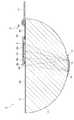
例えば、図4に示されるように、本体部2は、半球状のレンズがその平面部分と略直交し且つ互いに略平行な2つの平面で切り落とされた形状であってもよい。この場合には、半球状のレンズの平面部分が本体部2の前面2aとされ、半球状のレンズの曲面部分に分光部3が形成される。 For example, as shown in FIG. 4, the
また、図5に示されるように、本体部2は、半球状のレンズがその平面部分と略直交し且つ互いに略平行な2つの面で切り落とされた形状の光透過部材22の平面部分に、長方形薄板状の光透過部材21が光学樹脂やダイレクトボンディングによって貼り合わされたものであってもよい。この場合には、光透過部材21の前面が本体部2の前面2aとされ、光透過部材22の曲面部分に分光部3が形成される。Further, as shown in FIG. 5, the
また、図6に示されるように、レンズとして機能する光透過部材23と回折層14とは、例えば、レプリカ成型用の光透過性低融点ガラス等によって一体的に形成されていてもよい。これにより、製造工程を簡略化することができると共に、光透過部材23と回折層14との相対的な位置関係にずれが生じるのを防止することができる。Further, as shown in FIG. 6, the
1…分光モジュール、2…本体部、2a…前面(所定の面)、21…光透過部材(第1の光透過部材)、22…光透過部材、23…光透過部材(第2の光透過部材)、3…分光部、4…光検出素子、5…反射層、6…光吸収層(第1の光吸収層)、6a…光通過孔(第1の光通過孔)、6b…光通過孔(第2の光通過孔)、7…光吸収層(第2の光吸収層)、7a…光通過孔(第3の光通過孔)、7b…光通過孔(第4の光通過孔)、9…配線、9a…パッド部(第1のパッド部)、9b…パッド部(第2のパッド部)、9c…接続部、13…光反射防止層、14…回折層。DESCRIPTION OF
Claims (5)
Translated fromJapanese前記本体部の所定の面から前記本体部に入射した光を分光して前記所定の面側に反射する分光部と、
前記所定の面上に支持され、前記分光部によって分光されて反射された光を検出する光検出素子と、
前記所定の面に形成され、前記光検出素子と電気的に接続された配線と、を備え、
前記本体部は、前記所定の面を有する第1の光透過部材、及び前記分光部が設けられた第2の光透過部材を有することを特徴とする分光モジュール。A main body that transmits light;
A spectroscopic unit that splits light incident on the main body from a predetermined surface of the main body and reflects the light to the predetermined surface;
A light detecting element that is supported on the predetermined surface and detects light reflected and reflected by the spectroscopic unit;
Wherein formed on the predetermined surface, andawiring which is electricallyconnected to the light detectingelement,
Said body portion, the spectral module according to claim Rukototo having a second light transmitting member first light transmitting member, and that the spectroscopic portion is provided with the predetermined surface.
前記分光部は、前記曲面部分の外側表面に形成された回折層、及び前記回折層の外側表面に形成された反射層を有することを特徴とする請求項1〜4のいずれか一項記載の分光モジュール。BeforeStories second light transmitting member has a curved surface portion,
The spectroscopic unit, the diffraction layer formed on the outer surface of the curved portion, and any one of claims1 to4, wherein a reflective layer formed on the outer surface of the diffracting layer Spectroscopic module.
Priority Applications (1)
| Application Number | Priority Date | Filing Date | Title |
|---|---|---|---|
| JP2011251704AJP5097294B2 (en) | 2011-11-17 | 2011-11-17 | Spectroscopic module |
Applications Claiming Priority (1)
| Application Number | Priority Date | Filing Date | Title |
|---|---|---|---|
| JP2011251704AJP5097294B2 (en) | 2011-11-17 | 2011-11-17 | Spectroscopic module |
Related Parent Applications (1)
| Application Number | Title | Priority Date | Filing Date |
|---|---|---|---|
| JP2007153014ADivisionJP4887221B2 (en) | 2007-06-08 | 2007-06-08 | Spectroscopic module |
Publications (3)
| Publication Number | Publication Date |
|---|---|
| JP2012053067A JP2012053067A (en) | 2012-03-15 |
| JP2012053067A5 JP2012053067A5 (en) | 2012-06-07 |
| JP5097294B2true JP5097294B2 (en) | 2012-12-12 |
Family
ID=45906496
Family Applications (1)
| Application Number | Title | Priority Date | Filing Date |
|---|---|---|---|
| JP2011251704AActiveJP5097294B2 (en) | 2011-11-17 | 2011-11-17 | Spectroscopic module |
Country Status (1)
| Country | Link |
|---|---|
| JP (1) | JP5097294B2 (en) |
Family Cites Families (8)
| Publication number | Priority date | Publication date | Assignee | Title |
|---|---|---|---|---|
| JPS626126A (en)* | 1985-07-03 | 1987-01-13 | Shimadzu Corp | Sensor for optical spectrum analysis |
| DE4038638A1 (en)* | 1990-12-04 | 1992-06-11 | Zeiss Carl Fa | DIODE LINE SPECTROMETER |
| EP0942267B1 (en)* | 1998-03-11 | 2006-08-30 | Gretag-Macbeth AG | Spectrometer |
| US6885107B2 (en)* | 2002-08-29 | 2005-04-26 | Micron Technology, Inc. | Flip-chip image sensor packages and methods of fabrication |
| JP2004191246A (en)* | 2002-12-12 | 2004-07-08 | Matsushita Electric Ind Co Ltd | Unevenness detection sensor |
| JP2004309146A (en)* | 2003-04-02 | 2004-11-04 | Olympus Corp | Spectrophotometer |
| JP4409860B2 (en)* | 2003-05-28 | 2010-02-03 | 浜松ホトニクス株式会社 | Spectrometer using photodetector |
| JP4627410B2 (en)* | 2004-04-20 | 2011-02-09 | 浜松ホトニクス株式会社 | Measuring device using a spectrometer |
- 2011
- 2011-11-17JPJP2011251704Apatent/JP5097294B2/enactiveActive
Also Published As
| Publication number | Publication date |
|---|---|
| JP2012053067A (en) | 2012-03-15 |
Similar Documents
| Publication | Publication Date | Title |
|---|---|---|
| JP4887221B2 (en) | Spectroscopic module | |
| JP4891841B2 (en) | Spectroscopic module | |
| JP5325829B2 (en) | Spectroscopic module | |
| KR101735131B1 (en) | Spectroscopy module and manufacturing method therefor | |
| TWI451072B (en) | Spectral module | |
| US8045155B2 (en) | Spectroscopic module | |
| JP4891840B2 (en) | Spectroscopic module | |
| JP5335729B2 (en) | Spectroscopic module | |
| JP5512961B2 (en) | Spectroscopic module and manufacturing method thereof | |
| JP5205240B2 (en) | Spectroscopic module manufacturing method and spectroscopic module | |
| KR20100017082A (en) | Spectroscopic module | |
| WO2009139315A1 (en) | Spectral module | |
| JP4887251B2 (en) | Spectroscopic module | |
| JP4887250B2 (en) | Spectroscopic module | |
| WO2011027747A1 (en) | Spectral module | |
| JP5097294B2 (en) | Spectroscopic module | |
| JP5113947B2 (en) | Spectroscopic module | |
| JP4980184B2 (en) | Spectroscopic module | |
| JP5825880B2 (en) | Spectroscopic module |
Legal Events
| Date | Code | Title | Description |
|---|---|---|---|
| A521 | Request for written amendment filed | Free format text:JAPANESE INTERMEDIATE CODE: A523 Effective date:20120418 | |
| A871 | Explanation of circumstances concerning accelerated examination | Free format text:JAPANESE INTERMEDIATE CODE: A871 Effective date:20120824 | |
| TRDD | Decision of grant or rejection written | ||
| A975 | Report on accelerated examination | Free format text:JAPANESE INTERMEDIATE CODE: A971005 Effective date:20120910 | |
| A01 | Written decision to grant a patent or to grant a registration (utility model) | Free format text:JAPANESE INTERMEDIATE CODE: A01 Effective date:20120918 | |
| A01 | Written decision to grant a patent or to grant a registration (utility model) | Free format text:JAPANESE INTERMEDIATE CODE: A01 | |
| A61 | First payment of annual fees (during grant procedure) | Free format text:JAPANESE INTERMEDIATE CODE: A61 Effective date:20120921 | |
| R150 | Certificate of patent or registration of utility model | Ref document number:5097294 Country of ref document:JP Free format text:JAPANESE INTERMEDIATE CODE: R150 Free format text:JAPANESE INTERMEDIATE CODE: R150 | |
| FPAY | Renewal fee payment (event date is renewal date of database) | Free format text:PAYMENT UNTIL: 20150928 Year of fee payment:3 | |
| R250 | Receipt of annual fees | Free format text:JAPANESE INTERMEDIATE CODE: R250 | |
| R250 | Receipt of annual fees | Free format text:JAPANESE INTERMEDIATE CODE: R250 |