JP5087792B2 - Position detection device - Google Patents
Position detection deviceDownload PDFInfo
- Publication number
- JP5087792B2 JP5087792B2JP2008282399AJP2008282399AJP5087792B2JP 5087792 B2JP5087792 B2JP 5087792B2JP 2008282399 AJP2008282399 AJP 2008282399AJP 2008282399 AJP2008282399 AJP 2008282399AJP 5087792 B2JP5087792 B2JP 5087792B2
- Authority
- JP
- Japan
- Prior art keywords
- position detection
- unit
- display
- electrode
- indicator
- Prior art date
- Legal status (The legal status is an assumption and is not a legal conclusion. Google has not performed a legal analysis and makes no representation as to the accuracy of the status listed.)
- Active
Links
Images


Classifications
- G—PHYSICS
- G06—COMPUTING OR CALCULATING; COUNTING
- G06F—ELECTRIC DIGITAL DATA PROCESSING
- G06F3/00—Input arrangements for transferring data to be processed into a form capable of being handled by the computer; Output arrangements for transferring data from processing unit to output unit, e.g. interface arrangements
- G06F3/01—Input arrangements or combined input and output arrangements for interaction between user and computer
- G06F3/03—Arrangements for converting the position or the displacement of a member into a coded form
- G06F3/041—Digitisers, e.g. for touch screens or touch pads, characterised by the transducing means
- G06F3/0412—Digitisers structurally integrated in a display
- G—PHYSICS
- G06—COMPUTING OR CALCULATING; COUNTING
- G06F—ELECTRIC DIGITAL DATA PROCESSING
- G06F3/00—Input arrangements for transferring data to be processed into a form capable of being handled by the computer; Output arrangements for transferring data from processing unit to output unit, e.g. interface arrangements
- G06F3/01—Input arrangements or combined input and output arrangements for interaction between user and computer
- G06F3/03—Arrangements for converting the position or the displacement of a member into a coded form
- G06F3/033—Pointing devices displaced or positioned by the user, e.g. mice, trackballs, pens or joysticks; Accessories therefor
- G06F3/0354—Pointing devices displaced or positioned by the user, e.g. mice, trackballs, pens or joysticks; Accessories therefor with detection of 2D relative movements between the device, or an operating part thereof, and a plane or surface, e.g. 2D mice, trackballs, pens or pucks
- G—PHYSICS
- G06—COMPUTING OR CALCULATING; COUNTING
- G06F—ELECTRIC DIGITAL DATA PROCESSING
- G06F3/00—Input arrangements for transferring data to be processed into a form capable of being handled by the computer; Output arrangements for transferring data from processing unit to output unit, e.g. interface arrangements
- G06F3/01—Input arrangements or combined input and output arrangements for interaction between user and computer
- G06F3/03—Arrangements for converting the position or the displacement of a member into a coded form
- G06F3/041—Digitisers, e.g. for touch screens or touch pads, characterised by the transducing means
- G06F3/0416—Control or interface arrangements specially adapted for digitisers
- G06F3/04166—Details of scanning methods, e.g. sampling time, grouping of sub areas or time sharing with display driving
- G—PHYSICS
- G06—COMPUTING OR CALCULATING; COUNTING
- G06F—ELECTRIC DIGITAL DATA PROCESSING
- G06F3/00—Input arrangements for transferring data to be processed into a form capable of being handled by the computer; Output arrangements for transferring data from processing unit to output unit, e.g. interface arrangements
- G06F3/01—Input arrangements or combined input and output arrangements for interaction between user and computer
- G06F3/03—Arrangements for converting the position or the displacement of a member into a coded form
- G06F3/041—Digitisers, e.g. for touch screens or touch pads, characterised by the transducing means
- G06F3/0416—Control or interface arrangements specially adapted for digitisers
- G06F3/0418—Control or interface arrangements specially adapted for digitisers for error correction or compensation, e.g. based on parallax, calibration or alignment
- G06F3/04184—Synchronisation with the driving of the display or the backlighting unit to avoid interferences generated internally
- G—PHYSICS
- G06—COMPUTING OR CALCULATING; COUNTING
- G06F—ELECTRIC DIGITAL DATA PROCESSING
- G06F3/00—Input arrangements for transferring data to be processed into a form capable of being handled by the computer; Output arrangements for transferring data from processing unit to output unit, e.g. interface arrangements
- G06F3/01—Input arrangements or combined input and output arrangements for interaction between user and computer
- G06F3/03—Arrangements for converting the position or the displacement of a member into a coded form
- G06F3/041—Digitisers, e.g. for touch screens or touch pads, characterised by the transducing means
- G06F3/044—Digitisers, e.g. for touch screens or touch pads, characterised by the transducing means by capacitive means
- G—PHYSICS
- G06—COMPUTING OR CALCULATING; COUNTING
- G06F—ELECTRIC DIGITAL DATA PROCESSING
- G06F3/00—Input arrangements for transferring data to be processed into a form capable of being handled by the computer; Output arrangements for transferring data from processing unit to output unit, e.g. interface arrangements
- G06F3/01—Input arrangements or combined input and output arrangements for interaction between user and computer
- G06F3/03—Arrangements for converting the position or the displacement of a member into a coded form
- G06F3/041—Digitisers, e.g. for touch screens or touch pads, characterised by the transducing means
- G06F3/045—Digitisers, e.g. for touch screens or touch pads, characterised by the transducing means using resistive elements, e.g. a single continuous surface or two parallel surfaces put in contact
- G—PHYSICS
- G09—EDUCATION; CRYPTOGRAPHY; DISPLAY; ADVERTISING; SEALS
- G09G—ARRANGEMENTS OR CIRCUITS FOR CONTROL OF INDICATING DEVICES USING STATIC MEANS TO PRESENT VARIABLE INFORMATION
- G09G3/00—Control arrangements or circuits, of interest only in connection with visual indicators other than cathode-ray tubes
- G09G3/20—Control arrangements or circuits, of interest only in connection with visual indicators other than cathode-ray tubes for presentation of an assembly of a number of characters, e.g. a page, by composing the assembly by combination of individual elements arranged in a matrix no fixed position being assigned to or needed to be assigned to the individual characters or partial characters
- G09G3/34—Control arrangements or circuits, of interest only in connection with visual indicators other than cathode-ray tubes for presentation of an assembly of a number of characters, e.g. a page, by composing the assembly by combination of individual elements arranged in a matrix no fixed position being assigned to or needed to be assigned to the individual characters or partial characters by control of light from an independent source
- G09G3/3433—Control arrangements or circuits, of interest only in connection with visual indicators other than cathode-ray tubes for presentation of an assembly of a number of characters, e.g. a page, by composing the assembly by combination of individual elements arranged in a matrix no fixed position being assigned to or needed to be assigned to the individual characters or partial characters by control of light from an independent source using light modulating elements actuated by an electric field and being other than liquid crystal devices and electrochromic devices
- G09G3/3453—Control arrangements or circuits, of interest only in connection with visual indicators other than cathode-ray tubes for presentation of an assembly of a number of characters, e.g. a page, by composing the assembly by combination of individual elements arranged in a matrix no fixed position being assigned to or needed to be assigned to the individual characters or partial characters by control of light from an independent source using light modulating elements actuated by an electric field and being other than liquid crystal devices and electrochromic devices based on rotating particles or microelements
- G—PHYSICS
- G06—COMPUTING OR CALCULATING; COUNTING
- G06F—ELECTRIC DIGITAL DATA PROCESSING
- G06F3/00—Input arrangements for transferring data to be processed into a form capable of being handled by the computer; Output arrangements for transferring data from processing unit to output unit, e.g. interface arrangements
- G06F3/01—Input arrangements or combined input and output arrangements for interaction between user and computer
- G06F3/03—Arrangements for converting the position or the displacement of a member into a coded form
- G06F3/041—Digitisers, e.g. for touch screens or touch pads, characterised by the transducing means
- G06F3/044—Digitisers, e.g. for touch screens or touch pads, characterised by the transducing means by capacitive means
- G06F3/0444—Digitisers, e.g. for touch screens or touch pads, characterised by the transducing means by capacitive means using a single conductive element covering the whole sensing surface, e.g. by sensing the electrical current flowing at the corners
- G—PHYSICS
- G09—EDUCATION; CRYPTOGRAPHY; DISPLAY; ADVERTISING; SEALS
- G09G—ARRANGEMENTS OR CIRCUITS FOR CONTROL OF INDICATING DEVICES USING STATIC MEANS TO PRESENT VARIABLE INFORMATION
- G09G2300/00—Aspects of the constitution of display devices
- G09G2300/08—Active matrix structure, i.e. with use of active elements, inclusive of non-linear two terminal elements, in the pixels together with light emitting or modulating elements
Landscapes
- Engineering & Computer Science (AREA)
- Theoretical Computer Science (AREA)
- General Engineering & Computer Science (AREA)
- Physics & Mathematics (AREA)
- General Physics & Mathematics (AREA)
- Human Computer Interaction (AREA)
- Computer Hardware Design (AREA)
- Position Input By Displaying (AREA)
- Control Of Indicators Other Than Cathode Ray Tubes (AREA)
- Measurement Of Length, Angles, Or The Like Using Electric Or Magnetic Means (AREA)
Description
Translated fromJapanese 本発明は、位置検出装置に適用して好適な技術に関する。
より詳細には、透過性を損なうことなく表示機能を付加した新規な位置検出装置の技術に関する。The present invention relates to a technique suitable for application to a position detection device.
More specifically, the present invention relates to a technique for a novel position detection device to which a display function is added without impairing transparency.
コンピュータに位置情報を与える入力装置には、様々なものがある。その中で、例えば、タッチパネルと呼ばれる、位置情報入力装置がある。
タッチパネルは、例えば、液晶表示装置の表示エリアに指示位置を検出する位置検出装置を重ね合わせたもので、指や専用のペン等の位置指示器で表示画面に触れることで、コンピュータ等の操作を行なう入力装置である。指やペンが触れた位置を検知して画面上の位置を指定し、コンピュータに指示を与えるものである。
このタッチパネルは、PDA(Personal Digital Assistant)や銀行のATM(Automated Teller Machine)、駅の券売機等で広く利用されている。There are various input devices that provide position information to a computer. Among them, for example, there is a position information input device called a touch panel.
A touch panel is, for example, an overlay of a position detection device that detects an indicated position on the display area of a liquid crystal display device. By touching the display screen with a position indicator such as a finger or a dedicated pen, the touch panel can be operated. The input device to perform. A position touched by a finger or pen is detected, a position on the screen is designated, and an instruction is given to the computer.
This touch panel is widely used in personal digital assistants (PDAs), ATMs (Automated Teller Machines) of banks, ticket machines at stations, and the like.
このタッチパネルに採用される位置情報検出技術には、様々なものがある。例えば、圧力の変化で位置検出を行う抵抗膜方式や検出平面の表面の膜の静電容量の変化で位置検出を行う静電容量方式等がある。 There are various position information detection techniques employed in this touch panel. For example, there are a resistance film method that detects a position by a change in pressure, a capacitance method that detects a position by a change in capacitance of a film on the surface of a detection plane, and the like.
なお、本出願人の発明に係る従来技術を、特許文献1に示す。 The prior art relating to the applicant's invention is shown in Patent Document 1.
前述のタッチパネルに組み合わせられる位置検出装置は、特に指で指示した位置を検出する場合は、静電容量方式が採用されることが多い。静電容量方式の位置検出装置を表示装置に組み込む際には、表示装置の上に位置検出装置を重ね合わせることとなる。 The position detection device combined with the touch panel described above often employs a capacitance method particularly when detecting a position designated by a finger. When a capacitive position detection device is incorporated in a display device, the position detection device is overlaid on the display device.
近年、新しい表示装置の一形態として、電子ペーパーと呼ばれる表示装置が注目されている。この電子ペーパーは、帯電した着色粉体に電圧を印加することで、白黒等の濃淡や色を表示するものである。この電子ペーパーは、広く表示装置として使用されている液晶表示装置等に比べて消費電力が少なく、大幅な薄型化を実現できるので、静止画像やテキスト等を表示する用途を中心に普及しつつある。 In recent years, a display device called electronic paper has attracted attention as one form of a new display device. This electronic paper displays a shade and color such as black and white by applying a voltage to a charged colored powder. Since this electronic paper consumes less power than a liquid crystal display device or the like that is widely used as a display device and can realize a significant reduction in thickness, it is becoming increasingly popular mainly for displaying still images and text. .
ところで、かかる特徴を有する電子ペーパーにさらなる機能を追加したい、という要望がある。例えば、この電子ペーパーを通常の紙のように、メモを書いたり印や付箋を付けられるようにする、というものである。そこで、この電子ペーパーに、従来のタッチパネル装置と同様に、例えば、静電容量方式の位置検出装置を重ね合わせることで、かかる機能を付加することが考えられる。 By the way, there is a desire to add further functions to electronic paper having such characteristics. For example, this electronic paper can be written on a memo, a sticker or a sticky note, like ordinary paper. Therefore, it is conceivable to add such a function to this electronic paper, for example, by superimposing a capacitive position detection device on the electronic paper as in the conventional touch panel device.
ところが、静電容量方式等の位置検出装置を表示装置に搭載する場合には、その表示エリアに位置検出装置を重ねて合わせるので、表示エリアには複数の透明な部材を重ね合わさることになる。その結果、表示エリアの透過性が悪化する、という問題が発生する。さらに、複数の部材を重ね合わせているので、かかる機能を搭載しない表示装置よりも厚みが増してしまい、電子ペーパーの特徴である薄さを損なってしまうという問題も発生する。 However, when a position detection device such as a capacitance type is mounted on a display device, the position detection device is overlapped with the display area, and thus a plurality of transparent members are overlapped with the display area. As a result, there arises a problem that the transparency of the display area is deteriorated. Furthermore, since a plurality of members are superposed, the thickness is increased as compared with a display device not equipped with such a function, and there is a problem that the thinness that is characteristic of electronic paper is impaired.
本発明はかかる点に鑑みてなされたものであり、その目的は、透過性や薄さを損なうことなく表示機能を搭載した位置検出装置を提供することをである。 The present invention has been made in view of the above points, and an object of the present invention is to provide a position detection device equipped with a display function without impairing transparency and thinness.
上記課題を解決するために、本発明の位置検出装置は、第一の電極と、第二の電極と、第一の電極と第二の電極との間に介在配置された表示材料を備え、第一の電極と第二の電極との間への駆動電源の供給が停止した後も表示材料が表示状態を保持可能な表示部を備える。さらに、入力信号の供給に対応して表示部の表示駆動を行う表示駆動部と、この表示部が備える第一の電極を指示体による指示位置に共用して指示体による指示位置を検出する位置検出部と、入力信号の供給及び指示体の位置指示のそれぞれの有無に基づいて表示駆動部と位置検出部とを時分割動作させる際の駆動時間を制御する制御部とを備えている。In order to solve the above problems, a position detecting device of the present inventionincludes afirst electrode, a second electrode,the intervening arranged display material betweenthe firstelectrode andthe second electrode, also comprises a display unit capable of holding thedisplay material is a display state after the supply of the drive powerto betweenthe firstelectrode andthe second electrodestops. Furthermore, a display driving unit that performs display driving ofthe display unitin response to supply of aninput signal, and aposition that detects the indication position by the indicator by sharing the first electrode provided in the display unit with the indication position by the indicator A detection unit, anda control unit that controls a driving time when the display driving unit and the position detection unit are operated in a time-sharing manner based on the presence or absence of the supply of theinput signal and the position indication of the indicator.
本発明により、透過性を損なうことなく位置検出装置を搭載した表示装置を提供することができる。 According to the present invention, a display device equipped with a position detection device can be provided without impairing the transparency.
以下、本発明の実施の形態例について、図1〜図12を参照して説明する。Hereinafter,theimplementation of embodimentsof the present invention will be described with reference to FIGS. 1-12.
まず、本発明の実施形態例である位置検出装置の動作原理を図1及び図2を参照して、表示部である電子ペーパーの動作原理を図3及び図4を参照して、それぞれ簡単に説明する。First, the operation principleof the position detectiondevice according to theembodiment of thepresent invention will be briefly described with reference to FIGS. 1 and 2, and the operation principle of electronic paper as a display unit will be simply described with reference to FIGS. explain.
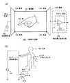
図1(a)は位置検出装置101の動作原理を説明する模式図であり、図1(b)は図1(a)の等価回路図である。位置検出装置101は、透明導電膜である電極膜102、接点104a〜104d、配線105a、105b、交流電圧源106、電流電圧変換回路108等を備えて構成される。
電極膜102は、例えば、酸化インジウムスズ(Indium Tin Oxide)よりなるITO膜や、酸化錫にアンチモンを添加したATO膜、酸化亜鉛にアルミニウムを添加したAZO膜などの透明導電性材料の膜である。この電極膜102の表面には図示しない薄い絶縁膜が貼付され、この絶縁膜を介して電極膜102の上を指103で触れるようになっている。そして、この電極膜102の四隅に接点104a、104b、104c及び104dが設けられている。この接点104aと104b、接点104cと104d同士はそれぞれ配線105a及び105bによって接続されている。
この配線105aは交流電圧源106に、配線105bはオペアンプ107aと抵抗R108bとからなる電流電圧変換回路108にそれぞれ接続されている。FIG. 1A is a schematic diagram for explaining the operation principle of the position detection apparatus 101, and FIG. 1B is an equivalent circuit diagram of FIG. The position detectiondevice 101 includes an
The
The
人体109は数pFのコンデンサと等価であるとみなすことができるので、この図1(b)中では、この等価なコンデンサを人体コンデンサC110として表している。一方、オペアンプ107aと抵抗R107bからなる電流電圧変換回路108の入力端子は、周知のイマジナルショート現象により等価的に導通しているとみなすことができる。そのため、交流電圧源106から発される交流電流は、電極膜102が形成する電極膜抵抗R111へ流れる電流と、電極膜102の途中に接触する人体コンデンサC110へ流れる電流との二手に分かれる。 Since the human body 109 can be regarded as equivalent to a capacitor of several pF, the equivalent capacitor is represented as a human body capacitor C110 in FIG. On the other hand, the input terminal of the current-
ここで、交流電圧源106が位置検出部101の配線105aに接続された場合と、配線105bに接続された場合とを図2を参照して説明する。なお、図2(a)は位置検出装置の動作原理を説明する模式図であり、図2(b)は図2(a)の等価回路である。また、図2(c)は位置検出装置の動作原理を説明する模式図であり、図2(d)は図2(c)の等価回路である。ここで、図2(a)と図2(c)との差異は、交流電圧源106とオペアンプ107が接続される配線が逆である点である。 Here, a case where the
図2(b)及び図2(d)に示した等価回路を比較すると、交流電圧源106から見たときの人体の指103が触れる位置は異なっている。このため、図2(b)と図2(d)とでは、電極膜102の抵抗R111と人体コンデンサC110とによって形成される合成インピーダンスが異なるので、電流電圧変換回路108で検出される電流が異なることになる。この電流の差を演算することで、指103が電極膜102上の左右方向の位置を検出することができるようになっている。Comparing the equivalent circuits shown in FIG. 2B and FIG. 2D, the positions touched by the
図2(a)及び(c)では、電極膜102の左右方向について指103の位置を検出したが、電極膜102の上下方向についても同様に、指103の位置を検出することができる。すなわち、上下方向の位置を検出するときには、電極膜102の四隅の接点の上側同士、すなわち接点104aと104cと、下側同士、すなわち接点104bと104dとをそれぞれ接続して、同様の処理を行う。 In FIGS. 2A and 2C, the position of the
以上のように、透明電極膜を用いた静電方式の位置検出装置は、透明電極膜の「上」「下」「左」「右」に交流電圧を印加し、それぞれで検出した電流の差を演算することで、透明電極膜上の指の位置を検出する。As describedabove, the position detecting device of an electrostatic method using atransparency electrode film, the AC voltage is applied to the "up", "down", "left", "right" of the transparent electrode film, the current detected by the respective The position of the finger on the transparent electrode film is detected by calculating the difference.
なお、人体の指103が電極膜102に接触することによって生じる影響を効果的に検出するために、位置検出装置では幾つかの技術的工夫を施している。例えば、交流電圧源106の周波数には、例えば、人体が最も吸収しやすいといわれる200kHz近辺を用いている。 In order to effectively detect the influence caused by the
次に、電子ペーパーの動作原理について、図3及び図4を参照して説明する。ここで、図3は電子ペーパーの原理を説明する模式図であり、図4は図3の等価回路である。なお、図3は電子ペーパーの模式的斜視図でもあり、図4は図3の模式的構成を真横から見たものと解釈することもできる。
電子ペーパー301は、マトリクス状に配置された複数の水平電圧線302及び垂直制御線305、水平選択スイッチ303等を備えている。水平電圧線302は水平選択スイッチ303を介して選択的に直流電圧源304に接続される。水平電圧線302と垂直制御線305との交点部分には、FET306が接続されている。FET306のドレインが水平電圧線302に、FET306のゲートが垂直制御線305にそれぞれ接続される。Next, the operation principle of electronic paper will be described with reference to FIGS. Here, FIG. 3 is a schematic diagram illustrating the principle of electronic paper, and FIG. 4 is an equivalent circuit of FIG. 3 is also a schematic perspective view of the electronic paper, and FIG. 4 can also be interpreted as a schematic configuration of FIG. 3 viewed from the side.
The electronic paper 301 includes a plurality of horizontal voltage lines 302, vertical control lines305 , a
各垂直制御線305は、それぞれカウンタ307に接続されている。各々のカウンタ307にはレジスタ308が接続されている。このレジスタ308に設定された計数値がカウンタ307に与えられると、カウンタ307はクロック生成器309から入力されるクロックを計数する。このクロックの計数値がレジスタ308から設定された計数値に達すると、出力を高レベル(H)から低レベル(L)に落とす。つまり、レジスタ308を通じてカウンタ307に設定された計数値は、FET306のオン時間である。
したがって、図3のカウンタ307は、図4の点線で囲んでいるスイッチ402と抵抗R403に相当し、スイッチのオン時間は、カウンタ307がHを出力する時間に相当する。Each vertical control line 305 is connected to a
Therefore, the
FET306のソースには、小さな電極プレート310が接続されている。この電極プレート310に対向して、接地された電極膜102が設けられている。この電極プレート310と電極膜102との間には、帯電した微粒子が封入された小さなビーズ311が挟まれている。 A
このビーズ311内には、黒色の微粒子と白色の微粒子が封入されている。このビーズ311内に封入された黒色の微粒子はマイナスに帯電され、白色の微粒子はプラスに帯電されている。そして、このビーズ311の一方の半球側に黒色の微粒子が、他方の半球側には白色の微粒子がそれぞれ封入され、一つのビーズ311を構成する。
そして、かかる構成を備えたビーズ311に電圧を印加すると、ビーズ311の中に封入された微粒子の電荷によりビーズが回転する。このビーズ311の回転は、電圧を印加する時間によって異なる。つまり、ドット毎の白黒の濃淡を、ビーズ311に対する電圧印加時間で制御することができる。In the
When a voltage is applied to the
なお、各ドット毎に白黒を表現するので、水平電圧線302に印加する電圧は、直流電圧源304のプラスだけでなく、マイナスも接続してビーズ311を回転させ、白から黒へ、黒から白へと変化させるようになっている。 In addition, since black and white are expressed for each dot, the voltage applied to the horizontal voltage line 302 is connected not only to the plus of the
以上のように、電子ペーパー301は、ビーズ311に電圧を印加した後、その電圧の印加を止めても、ビーズ311の向きが回転後の状態で保たれるので、表示内容が保持される。このように、電子ペーパー301は、一度駆動を行った後は電圧を印加し続けなくても表示状態を保持できるので、一般的な液晶ディスプレイ(LCD)等と比べると、消費電力の面で優れている。 As described above, the electronic paper 301 retains the display content because the orientation of the
ところで、位置検出装置101と電子ペーパー301とは、それぞれ電極膜102を有している、という共通点がある。そこで、本発明は、この電極膜102を位置検出装置101と電子ペーパー301の双方で時分割にて排他的に共有するようにしている。By the way, the position detection apparatus 101 and the electronic paper 301 have a common point that each has the
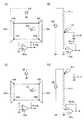
次に、本発明の第一の実施の形態例における位置検出装置501を図5に従って説明する。この図5は、位置検出装置501の概略ブロック図である。
位置検出装置501は、表示駆動部502と、位置検出部503と、マトリクスゲート504と、表示部505とから構成されている。
表示駆動部502は、表示部505を駆動するものである。表示部505は、例えば、ITO膜等の透明導電膜からなる電極膜102と、マトリクスゲート504とからなり、表示駆動部502により表示駆動されて、外部から入力されたビデオ信号に基づき画像やテキスト等を表示する。
位置検出部503は、表示部505の電極膜102上を指等の指示体により指示した位置を検出する回路部である。ここで、表示駆動部502と位置検出部503とは排他的に電極膜102を占有するため、その排他制御は表示駆動部502が行う。Next,the position detection device 501in the first embodiment ofthe present invention will be described with reference to FIG. FIG. 5 is a schematic block diagram of the position detection device 501.
The position detection device 501 includes a
The
The
表示駆動部502は、ビデオ信号に基づく表示駆動を行う際に、位置検出部503に対して制御信号を出力するようになっている。この制御信号は、表示駆動を開始するときに、「これから電子ペーパーの表示駆動を行う」旨を示す、表示更新信号である。同様に、位置検出部503は、表示駆動部502に対して二種類の制御信号を出力するようになっている。この制御信号は、「指の検出処理を完了した」旨を示す、検出完了信号と、「現在電極膜上には指が存在する/しない」旨を示す指存在信号である。 The
マトリクスゲート504は、図3にて示した水平電圧線302と、垂直制御線305と、水平電圧線302と垂直制御線305との各交点に存在するFET306と、電極プレート310とから構成される。この図5では図示はしていないが、マトリクスゲート504と電極膜102との間にはビーズ311が介在して設けられている。このマトリクスゲート504と電極膜102と、図示しないビーズ311とで、表示部505は構成されている。 The
表示駆動部502は、例えば、パソコン等の上位装置からビデオ信号が入力されると、マトリクスゲート504を通じて、マトリクスゲート504と電極膜102との間に介在しているビーズ311を電圧駆動する。このビデオ信号に基づく表示駆動を開始するときに、表示駆動部502は位置検出部503に対して表示更新信号を出力する。 For example, when a video signal is input from a host device such as a personal computer, the
位置検出部503は、電極膜102に「上」「下」「左」「右」に交流電圧を印加し、電流を検出することで指の存在の有無を検出し、指が存在する際にはその位置を検出する。この指の検出処理を行った後、位置検出部503は表示駆動部502に対して検出完了信号を出力する。また、位置検出部503は、電極膜102上に指103が存在しているか否かを、指存在信号にて出力する。 The
次に、図5に示した表示駆動部502と位置検出部503と表示部505との接続関係を図6に従って詳述する。この図6は、図5に示した位置検出装置501のうち電極膜102の周囲の構成をより詳細に説明するためのブロック図である。
電極膜102の四隅には、モード切替スイッチ602a、602b、602c及び602dが設けられている。このモード切替スイッチ602a、602b、602c及び602dの一方の端子は、表示駆動部502に接続されている。これら端子は電極膜102に共通の電位を与えるためのものである。このため、これら端子同士も接続されている。
モード切替スイッチ602a、602b、602c及び602dの他方の端子は、位置検出部503に接続されている。これら端子は、前述したように、電極膜102の「上」「下」「左」「右」に交流電圧を順番に印加し、電流を検出するため、位置検出部503に接続されている。なお、このモード切替スイッチ602a、602b、602c及び602dの切替制御は、表示駆動部502によって行われる。Next, the connection relationship among the
At the four corners of the
The other terminals of the
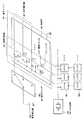
次に、図5に示した表示駆動部502と位置検出部503とを図7及び図8に従って詳述する。ここで、図7は、表示駆動部502及び位置検出部503の内部の構成ブロックを詳細に説明するための図、図8は位置検出部503の詳細ブロック図である。主に図7の信号処理部702の内部を詳述する図である。
図7に示すように、上位装置が出力したビデオ信号は、表示駆動部502に入力される。このビデオ信号は、表示駆動部502内の信号処理部702でビデオデータに変換される。このビデオデータはフレーム毎に第一フレームメモリ703に格納される。
ここで、表示駆動部502は、第一フレームメモリ703と同一容量の第二フレームメモリ704を備えており、この第二フレームメモリ704は、表示部505を構成する各々のビーズ311の表示状態を記憶している。
差分抽出部705は、第一フレームメモリ703と第二フレームメモリ704との間の差分データを作成して、表示駆動制御部706に送る。
このマイコンよりなる表示駆動制御部706は、差分データに基づいてマトリクスゲート504の駆動制御を行う。そして、表示駆動制御部706は、マトリクスゲート504の駆動制御を行った後、その結果を第二フレームメモリ704に反映させる。Next, the
As shown in FIG. 7, the video signal output from the host device is input to the
Here, the
The
The display
さらに、表示駆動制御部706は、位置検出部503との時分割制御を実現するために、位置検出部503内の位置算出及び制御部712に表示更新信号を送信すると共に、位置算出及び制御部712から検出完了信号及び指存在信号を受信する。
ここで、表示駆動部502は、位置検出部503が位置検出動作を実行している期間は表示駆動ができない。そこで、表示駆動制御部706は、表示駆動制御を行わないときには、第二フレームメモリ704の更新作業を停止する。これが表示駆動制御部706から第二フレームメモリ704に供給される更新制御信号である。Further, the display
Here, the
電極膜102の四隅に接続されているモード切替スイッチ602a、602b、602c及び602dは、表示更新信号と検出完了信号とが入力されるANDゲート707の出力信号によって切替制御が行われる。この表示更新信号と検出完了信号とが共に論理の真(H)であるときには、モード切替スイッチ602a、602b、602c及び602dは表示駆動部502側に接続される。 The mode change-over
この電極膜102の四隅に接続されているモード切替スイッチ602a、602b、602c及び602dの端子は、それぞれ四つの入出力切替スイッチ802a、802b、802c及び802dに接続される。この入出力切替スイッチ802a、802b、802c及び802dは、交流電圧源であるサイン波生成部803の出力と電流電圧変換回路を構成するオペアンプ107の反転入力とを選択的に切り換える。
この四つの入出力切替スイッチ802a、802b、802c及び802dを切替制御することで、電極膜102の「上」「下」「左」「右」に交流電圧を順番に印加し、電流を検出することができる。The terminals of the
By switching and controlling the four input /
オペアンプ107の出力信号は、ノイズ除去のためのバンドパスフィルタ804に入力される。なお、このバンドパスフィルタ804の中心周波数は、サイン波生成部803が生成する信号の周波数と同一に設定されている。
バンドパスフィルタ804の出力信号は、サイン波生成部803が生成する交流電圧信号と共に、アナログ乗算器からなる同期検波部805に入力される。
この同期検波部805の出力信号は、積分器806に入力されて、積分処理が行われる。なお、積分処理は積分器806の後段に接続されたA/D変換器807がA/D変換処理を完了したらリセットしなければならないので、リセット信号が位置算出及び制御部712から入力されるようになっている。The output signal of the
The output signal of the
The output signal of the
A/D変換器807は、積分器806の出力信号をデジタルデータに変換し、マイコンからなる位置算出及び制御部712に出力する。この位置算出及び制御部712は、入出力切替スイッチ802a、802b、802c及び802dの切替制御、サイン波生成部803のサイン波出力タイミングの制御、積分器806に出力するリセット信号の生成及びA/D変換器807の変換トリガ信号の生成を行う。そして、A/D変換器807から得られるデジタルデータから、指の有無の検出と指の位置のデータを演算して出力する。 The A /
ところで、位置検出部503による指示体の指示位置の検出は、常時行われていることが望ましい。位置検出部503は指等の指示体による位置指示がいつ開始されるかは分からないので、検出を停止している時間が長いと追従性が損なわれてしまうからである。
通常、マウス等のポインティングデバイスの要求仕様は、位置指示体(ポインタ)の位置をおよそ10msec間隔で取得できることといわれる。上述の位置検出部503による指示体の検出動作は、電極膜102の「上」「下」「左」「右」に交流電圧を順番に印加し、電流を検出することにより行う。したがって、位置検出部503のみを行うのであれば、2.5msec間隔で「上」「下」「左」「右」に交流電圧を順番に印加すればよいことになる。
しかしながら、本実施形態では、表示駆動部502と位置検出部503とが一の電極膜102を排他的に利用している。つまり、表示駆動部502が表示制御をしているときは、位置検出部503は位置検出を行うことができない。
そこで、表示させる内容に変化がない限り、位置検出部503による検出動作を優先し、表示させる内容の変化が生じたら、表示駆動部502の動作を位置検出部503の検出動作の間に割り込ませるようにしている。By the way, it is desirable that the
Usually, it is said that the required specification of a pointing device such as a mouse can acquire the position of a position indicator (pointer) at intervals of about 10 msec. The indicator detection operation by the
However, in the present embodiment, the
Therefore, as long as there is no change in the content to be displayed, the detection operation by the
図9は、表示駆動部502及び位置検出部503の動作状態を説明する状態遷移図である。各状態S901〜S904中、グラフで示したイラストはANDゲート707の出力の反転信号を示している。これは、論理の真の時に指の検出動作を行う、という説明をするために設けている。 FIG. 9 is a state transition diagram illustrating operation states of the
上位装置から表示駆動部502にビデオ信号が入力されておらず、かつ指示体も検出されていない状態であるときは、表示駆動部502は表示駆動を行う必要がないので、位置検出部503は常時、位置検出動作を行う(S901)。
そして、位置検出部503が位置検出動作を行った結果、指の存在を検出したときは、上位装置からビデオ信号の入力がない場合には、状態S901と同様に、位置検出部503が常時位置検出動作を継続する(S902)。When no video signal is input from the host device to the
When the
状態S901において、上位装置から表示駆動部502にビデオ信号が入力されると、位置検出部503の動作は指の存在を検出する最低限の動作に留め、駆動時間の大半を表示駆動部502に割り当てる(S903)。In a state S901, when a video signal is input from the host device to the
また、状態S902において、上位装置から表示駆動部502にビデオ信号が入力されると、表示駆動部502が表示制御を行いつつ、位置検出部503は指示位置を検出するために、表示駆動部502の動作よりも位置検出部503による指示体の検出を優先するために、駆動時間を表示駆動部502よりも位置検出部503へ長めに割り当てる(S904)。
同様に、状態S903において、位置検出部503が指示体による位置指示を検出すると、指示体の動きをしっかりトレースするために、状態S904に移行する。In a state S902, when a video signal is input from the host device to the
Similarly, when the
以上、図9を参照して説明したように、特定の状態(S904)のときは、表示駆動部502と位置検出部503とはそれぞれ交互に動作しなければならないので、位置検出部503の動作時間を制限する必要がある。なお、位置検出部503の位置検出動作の1サイクルは、10msecを下回らなければならない。更に言うならば、表示駆動部502とその占有時間を折半できることが望ましい。電子ペーパーである表示駆動部502の表示処理は、高速に動作し難いからである。具体的には、一例として、表示駆動部は5〜6msec、位置検出部503は4〜5msecを1サイクルとして動作し得ることが望ましい。この仕様では、電極膜102の「上」「下」「左」「右」に交流電圧を順番に印加し、電流を検出する4段階のサイクルは、各段階が1msecで完結することが望ましい。 As described above with reference to FIG. 9, in the specific state (S904), the
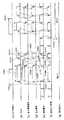
次に、表示駆動部502及び位置検出部503から出力される各種制御信号について図10を参照して説明する。この図10(a)、(b)、(c)、(d)、(e)、(f)及び(g)は、表示駆動部502及び位置検出部503の、各種信号及び状態のタイミングチャートである。
ここで、図10(a)はビデオ信号を示している。上位装置からビデオ信号が来ると、その期間を論理の真で模式的に表している。
図10(b)はタイマが出力する論理値を示す。このタイマは表示駆動制御部706の内部に、プログラムによって実現される。
図10(c)は表示更新信号を示す。この信号は、表示駆動部502が位置検出部503に対して表示動作を行いたい、との意思を伝える信号である。
図10(d)は表示駆動部が表示動作を行っている状態を示す。この仮想的な信号波形は、論理の真の時に表示駆動部が表示動作を行っていることを示す。
図10(e)は位置検出部503が位置検出動作を行っている状態を示す。この仮想的な信号波形は、論理の真の時に位置検出部503が位置検出動作を行っていることを示す。
図10(f)は検出完了信号を示す。この信号は、位置検出部503が表示駆動部502に対して指の位置検出動作を完了したことを報告する信号である。表示駆動部502は、表示更新信号を真に設定してから、この信号が真になったことを受けて、表示動作を実行する。
図10(g)は指存在信号を示す。この信号は、位置検出部503が指の存在を検出したことを示す信号である。Next, various control signals output from the
Here, FIG. 10A shows a video signal. When a video signal comes from the host device, the period is schematically represented by a logical truth.
FIG. 10B shows logical values output by the timer. This timer is realized in the display
FIG. 10C shows a display update signal. This signal is a signal that informs the
FIG. 10D shows a state in which the displaydriving unit is performing a display operation. This virtual signal waveform indicates that the displaydrive unit is performing a display operation when the logic is true.
FIG. 10E shows a state where the
FIG. 10F shows a detection completion signal. This signal is a signal for reporting that the
FIG. 10G shows a finger presence signal. This signal is a signal indicating that the
表示駆動制御部706は、上位装置からビデオ信号が入力され、ビーズ311による表示内容を変更する必要が生じたことを、差分抽出部705を通じて検知すると、位置算出及び制御部712に「表示駆動要求」を通知すべく、表示更新信号を論理の「偽」から「真」に転換する。しかし、このときは殆どの場合、位置検出部503は指の検出動作の途中である(S1001)。そこで、位置算出及び制御部712は、表示更新信号が真になってから直後の検出動作の終了を待った後、検出完了信号を「偽」から「真」に転換させると共に、指の検出動作を一時停止する(S1002)。 When the display
表示駆動制御部706は、検出完了信号が「真」になったことを検出すると、内部のタイマをオン動作させる(S1003)。このタイマは、表示駆動部502が表示駆動動作を行う時間を規定する。つまり、タイマが「真」を示している間だけ、表示駆動部502が表示駆動動作を行う(S1004)。これは、表示駆動制御部706は、タイマが規定する時間内に表示更新作業を完遂できていない場合でも、時間切れで表示更新作業を中断することを意味する。 When the display
表示駆動制御部706は、タイマが所定時間を計測すると、表示更新信号を「真」から「偽」に転換させると共に(S1005)、表示動作を停止する(S1006)。
位置算出及び制御部712は、表示更新信号が「真」から「偽」に転換したことを検出すると(S1007)、検出完了信号を「真」から「偽」に転換させると共に(S1008)、指検出動作を再開する(S1009)。When the timer measures a predetermined time, the display
Upon detecting that the display update signal has changed from “true” to “false” (S1007), the position calculation and
表示駆動制御部706は、上位装置からビデオ信号が与えられていなくても、直前の表示更新作業がタイマによる時間切れで中断されたことにより、未だビーズ311による表示内容を変更する必要があることを、差分抽出部705を通じて検知すると、再度、位置算出及び制御部712に「表示駆動要求」を通知すべく、表示更新信号を論理の「偽」から「真」に転換する。しかし、このときは殆どの場合、位置検出部503は指の検出動作の途中である(S1010)。そこで、位置算出及び制御部712は表示更新信号が真になってから直後の検出動作の終了を待つと、検出完了信号を「偽」から「真」に転換させると共に、指の検出動作を一時停止する(S1011)。 Even if no video signal is given from the host device, the display
表示駆動制御部706は、検出完了信号が「真」になったことを検出すると、内部のタイマをオン動作させる(S1012)。タイマが「真」を示している間だけ、表示駆動部502は表示駆動動作を行う(S1013)。
表示駆動動作が一通り完遂すると、第一フレームメモリ703の内容と第二フレームメモリ704の内容とが完全に一致する。つまり、表示更新作業が不要になる。表示駆動部は、このことを差分抽出部705から検知すると、表示動作を止めて、タイマをリセットさせる(S1014)。When the display
When the display drive operation is completed, the contents of the
タイマがリセットされると、タイマの出力は、論理の「真」から「偽」に転換する。表示更新信号はこれを受けて、論理の「真」から「偽」に転換する(S1015)。
位置算出及び制御部712は、表示更新信号が「真」から「偽」に転換したことを検出すると(S1016)、検出完了信号を「真」から「偽」に転換させると共に(S1017)、指検出動作を再開する(S1018)。When the timer is reset, the output of the timer changes from logic "true" to "false". In response to this, the display update signal changes from logic “true” to “false” (S1015).
Upon detecting that the display update signal has changed from “true” to “false” (S1016), the position calculation and
表示駆動制御部706は、指存在信号(図10(g))の論理状態に応じて、タイマの計時時間を切替える。このため、表示駆動制御部706が指の存在を検出した後(S1019)の、タイマの計時時間(T1021)は、指の存在を検出していない時の計時時間(T1020)よりも短い。The display
以上説明したように、本発明の第一の実施の形態例における位置検出装置501においては、電極膜102を表示駆動部502と位置検出部503との双方で時分割にて排他的に共有する、という技術的思想を開示した。この電極膜102を表示駆動部502と位置検出部503との双方で共有する方法としては、時分割の他に、周波数領域で分けて共有する方法もある。
以下、この技術思想に基づく本発明の第二の実施の形態例を、図11及び図12を参照して説明する。ここで、図11は、本発明の第二の実施の形態例における位置検出装置1011の概略ブロック図である。
この本発明の第二の実施の形態例における位置検出装置1011と、第一の実施の形態の例における位置検出装置501との相違点は、表示駆動部502と位置検出部1103との間で、表示更新信号、検出完了信号、指存在信号のやりとりを行わない点である。その他の点に関しては、第一の実施の形態例と同一なので、詳細な説明は省略する。As described above, in the position detection device 501 according to the first embodiment of the present invention, the
Hereinafter, a second embodiment of the present invention based on this technical concept will be described with reference to FIGS. Here, FIG. 11 is a schematic block diagram of the position detection apparatus 1011 in the second embodiment of the present invention.
The difference between the position detection device1011 in the second embodiment of the present invention and the position detection device 501 in the first embodiment is that the
ここで、本発明の第二の実施の形態例における位置検出部1103について、図12を参照して詳述する。この図12は、本発明の第二の実施の形態例における位置検出部1103の詳細ブロック図である。
この第二の実施の形態例においては、電極膜102の四隅には、第一の実施の形態例におけるモード切替スイッチ602a、602b、602c及び602dの代わりに、電流検出回路1202a、1202b、1202c及び1202dが設けられている。
この電流検出回路1202a、1202b、1202c及び1202dは、サイン波スイッチ1203a、1203b、1203c及び1203d及び電流検出スイッチ1204a、1204b、1204c及び1204dに接続されている。Here, the
In the second embodiment, at the four corners of the
The
この電流検出回路1202a、1202b、1202c及び1202dは、オペアンプ1217及び抵抗R1218からなる電流電圧変換回路と、オペアンプ1217の正極側入力端子にオフセット電圧を与えるための抵抗R1214及びR1215と、サイン波電圧信号を印加するコンデンサC1216とからなる。
オフセット電圧を与えるための抵抗R1214及びR1215は、表示駆動部502に対し、電極膜102を表示部505の一部として動作させるために設けられている。つまり、オペアンプ1217のイマジナルショート現象を利用して、電極膜102に一定の基準電圧を印加している。
サイン波生成部803から生じるサイン波電圧信号は、サイン波スイッチ1203aとコンデンサC1216とを通じて、オペアンプ1217の正極側入力端子に印加される。つまり、オペアンプ1217のイマジナルショート現象を利用して、電極膜102に交流電圧を印加する。The
Resistors R1214 and R1215 for providing an offset voltage are provided for causing the
The sine wave voltage signal generated from the
このサイン波スイッチ1203aは、サイン波生成部803と接続されているときは、電流検出スイッチ1204aがオフになり、逆に、サイン波スイッチ1203aがサイン波生成部803と接続されていないときは、電流検出スイッチ1204aはオンとなる。
そして、電流検出回路1202a、1202b、1202c及び1202dから電流検出スイッチ1204a、1204b、1204c及び1204dを通じて得られる出力信号は、バンドパスフィルタ804に入力される。このバンドパスフィルタ804以降の信号処理は、第一の実施形態と同じであるので、詳細な説明は省略する。When the
Output signals obtained from the
以上、本発明の実施形態例について説明したが、本発明は上記実施形態例に限定されるものではなく、特許請求の範囲に記載した本発明の要旨を逸脱しない限りにおいて、他の変形例、応用例を含む。 The embodiment of the present invention has been described above. However, the present invention is not limited to the above-described embodiment, and other modifications may be made without departing from the gist of the present invention described in the claims. Includes application examples.
例えば、上記第一及び第二の実施の形態例においては、指示体の例として人の指を例示しているが、本発明はこれに限定されるものではない。すなわち、電子ペーパー301を構成する電極膜102に、例えば、マトリクス状に複数の電極を設けた電極膜を採用した場合、すなわち、既存の電磁誘導方式の位置検出装置や静電結合方式の位置検出装置と、この電子ペーパーとを組み合わせてもよい。これらの場合には、それぞれの位置検出装置専用の指示体、すなわち、所定の周波数で共振する共振回路を搭載する位置指示器(ペン)や、静電結合ペンを用いることができる。 For example, in the first and second embodiments, a human finger is illustrated as an example of the indicator, but the present invention is not limited to this. That is, for example, when an electrode film provided with a plurality of electrodes in a matrix is used as the
102…電極膜、103…指、104a、104b、104c、104d…接点、105a、105b…配線、106…交流電圧源、107a…オペアンプ、R107b…抵抗、108…電圧電流変換回路、109…人体、C110…人体コンデンサ、R111…電極膜抵抗、302…水平電圧線、303…水平選択スイッチ、304…直流電圧源、305…垂直制御線、306…FET、307…カウンタ、308…レジスタ、310…電極プレート、311…ビーズ、501…位置検出装置、502…表示駆動部、503…位置検出部503、504…マトリクスゲート、505…表示部、602a、602b、602c、602d…モード切替スイッチ、702…信号処理部、703…第一フレームメモリ、704…第二フレームメモリ、705…差分抽出部、706…表示駆動制御部、707…ANDゲート、712…位置算出、制御部、802a、802b、802c、802d…入出力切替スイッチ、803…サイン波生成部、804…バンドパスフィルタ、805…同期検波部、806…積分器、807…A/D変換器、1011…位置検出装置、1202a、1202b、1202c、1202d…電流検出回路、1203a、1203b、1203c、1203d…サイン波スイッチ、1204a、1204b、1204c、1204d…電流検出スイッチ、1217…オペアンプ、R1214、R1215、R1218…抵抗、C1216…コンデンサ DESCRIPTION OF
Claims (7)
Translated fromJapanese入力信号の供給に対応して前記表示部の表示駆動を行う表示駆動部と、
前記表示部が備える前記第一の電極を指示体による指示位置に共用して前記指示体による指示位置を検出する位置検出部と、
前記入力信号の供給及び前記指示体の位置指示のそれぞれの有無に基づいて前記表示駆動部と前記位置検出部とを時分割動作させる際の駆動時間を制御する制御部と、
を備えたことを特徴とする位置検出装置。Afirst electrode, a second electrode,with an intervening arranged display materialbetween saidfirst electrode and said second electrode,between thefirst electrode and the second electrode A display unit capable of maintaining the display state of thedisplay material even after the supplyof drive power tois stopped,
A display driving unit that performs display driving of the display unitin response to supply of an input signal ;
A position detection unitfor detecting an indication position by the indicator by sharing the first electrode provided in the display unit with an indication position by the indicator ;
A control unit that controls a driving time when the display driving unit and the position detection unit are operated in a time-sharing manner based on the presence of each of the input signal supply and the position indication of the indicator;
A position detection device comprising:
Priority Applications (5)
| Application Number | Priority Date | Filing Date | Title |
|---|---|---|---|
| JP2008282399AJP5087792B2 (en) | 2008-10-31 | 2008-10-31 | Position detection device |
| US12/581,069US8780056B2 (en) | 2008-10-31 | 2009-10-16 | Position detecting device including display function |
| KR1020090103889AKR101531420B1 (en) | 2008-10-31 | 2009-10-30 | Position detecting device |
| EP09013715.9AEP2182426B1 (en) | 2008-10-31 | 2009-10-30 | Position detecting device |
| CN200910209225.7ACN101727241B (en) | 2008-10-31 | 2009-11-02 | Position detecting device |
Applications Claiming Priority (1)
| Application Number | Priority Date | Filing Date | Title |
|---|---|---|---|
| JP2008282399AJP5087792B2 (en) | 2008-10-31 | 2008-10-31 | Position detection device |
Publications (3)
| Publication Number | Publication Date |
|---|---|
| JP2010108428A JP2010108428A (en) | 2010-05-13 |
| JP2010108428A5 JP2010108428A5 (en) | 2011-11-24 |
| JP5087792B2true JP5087792B2 (en) | 2012-12-05 |
Family
ID=41566283
Family Applications (1)
| Application Number | Title | Priority Date | Filing Date |
|---|---|---|---|
| JP2008282399AActiveJP5087792B2 (en) | 2008-10-31 | 2008-10-31 | Position detection device |
Country Status (5)
| Country | Link |
|---|---|
| US (1) | US8780056B2 (en) |
| EP (1) | EP2182426B1 (en) |
| JP (1) | JP5087792B2 (en) |
| KR (1) | KR101531420B1 (en) |
| CN (1) | CN101727241B (en) |
Families Citing this family (14)
| Publication number | Priority date | Publication date | Assignee | Title |
|---|---|---|---|---|
| US9703411B2 (en) | 2009-04-30 | 2017-07-11 | Synaptics Incorporated | Reduction in latency between user input and visual feedback |
| TWI395126B (en)* | 2009-07-20 | 2013-05-01 | Mstar Semiconductor Inc | Sensing apparatus and method applied to touch screen |
| JP5430339B2 (en) | 2009-10-19 | 2014-02-26 | 株式会社ワコム | Position detecting device and position indicator |
| JP5528926B2 (en)* | 2010-07-09 | 2014-06-25 | 株式会社ジャパンディスプレイ | Detection device and display device |
| JP5358528B2 (en)* | 2010-07-21 | 2013-12-04 | 信越ポリマー株式会社 | Capacitive sensor sheet |
| CN102346048A (en)* | 2010-08-02 | 2012-02-08 | 纬创资通股份有限公司 | Sensing device and sensing method for saving electric energy |
| CN102156565B (en)* | 2010-12-31 | 2014-11-05 | 深圳超多维光电子有限公司 | Display equipment and method, and naked eye three-dimensional display device |
| CN102129324B (en)* | 2011-03-17 | 2012-05-02 | 汉王科技股份有限公司 | Touch device, control method thereof and electronic equipment with touch device |
| CN102880371B (en)* | 2011-07-15 | 2015-11-25 | 深圳市比亚迪电子部品件有限公司 | A kind of waken system of resistive touch screen |
| JP5925896B2 (en)* | 2011-09-07 | 2016-05-25 | シナプティクス インコーポレイテッド | Capacitive detection during hidden update time |
| CN103941939B (en)* | 2013-12-27 | 2018-02-06 | 上海天马微电子有限公司 | Touch screen, liquid crystal display device and scanning method thereof |
| WO2016186191A1 (en)* | 2015-05-21 | 2016-11-24 | 株式会社ワコム | Active stylus |
| TWI560680B (en)* | 2015-07-07 | 2016-12-01 | E Ink Holdings Inc | Electronic paper display apparatus and detection method thereof |
| US10146379B2 (en)* | 2015-11-23 | 2018-12-04 | Himax Technologies Limited | Touch screen capable of detecting touch pressure and a system of controlling the same |
Family Cites Families (17)
| Publication number | Priority date | Publication date | Assignee | Title |
|---|---|---|---|---|
| JPS5994736A (en)* | 1982-11-22 | 1984-05-31 | Toshiba Corp | Liquid crystal display device |
| US5194852A (en)* | 1986-12-01 | 1993-03-16 | More Edward S | Electro-optic slate for direct entry and display and/or storage of hand-entered textual and graphic information |
| US5392058A (en)* | 1991-05-15 | 1995-02-21 | Sharp Kabushiki Kaisha | Display-integrated type tablet device |
| US5610629A (en)* | 1991-12-06 | 1997-03-11 | Ncr Corporation | Pen input to liquid crystal display |
| JP2626595B2 (en)* | 1994-11-17 | 1997-07-02 | 日本電気株式会社 | Active matrix type liquid crystal display integrated tablet and driving method thereof |
| JPH08297267A (en)* | 1995-04-25 | 1996-11-12 | Alps Electric Co Ltd | Liquid crystal display device with tablet |
| JP3434415B2 (en) | 1996-07-05 | 2003-08-11 | アルプス電気株式会社 | Coordinate input device |
| US6323989B1 (en)* | 1996-07-19 | 2001-11-27 | E Ink Corporation | Electrophoretic displays using nanoparticles |
| JPH09138385A (en)* | 1996-09-17 | 1997-05-27 | Seiko Precision Kk | Ferroelectric liquid crystal touch panel device |
| TWI245252B (en)* | 2002-07-18 | 2005-12-11 | Gigno Technology Co Ltd | LCD and the touch-control method thereof |
| JP2007206845A (en)* | 2006-01-31 | 2007-08-16 | Wacom Co Ltd | Information processor |
| JP2007225875A (en)* | 2006-02-23 | 2007-09-06 | Bridgestone Corp | Information display device |
| US8144115B2 (en)* | 2006-03-17 | 2012-03-27 | Konicek Jeffrey C | Flat panel display screen operable for touch position determination system and methods |
| KR101274034B1 (en)* | 2006-08-25 | 2013-06-12 | 삼성디스플레이 주식회사 | Touch screen display device and method of manufacturing the same |
| US8125456B2 (en)* | 2007-01-03 | 2012-02-28 | Apple Inc. | Multi-touch auto scanning |
| GB2447983A (en)* | 2007-03-30 | 2008-10-01 | Seiko Epson Corp | Electrochromic display apparatus and method for operating said display apparatus |
| US8040326B2 (en)* | 2007-06-13 | 2011-10-18 | Apple Inc. | Integrated in-plane switching display and touch sensor |
- 2008
- 2008-10-31JPJP2008282399Apatent/JP5087792B2/enactiveActive
- 2009
- 2009-10-16USUS12/581,069patent/US8780056B2/enactiveActive
- 2009-10-30EPEP09013715.9Apatent/EP2182426B1/ennot_activeNot-in-force
- 2009-10-30KRKR1020090103889Apatent/KR101531420B1/ennot_activeExpired - Fee Related
- 2009-11-02CNCN200910209225.7Apatent/CN101727241B/enactiveActive
Also Published As
| Publication number | Publication date |
|---|---|
| KR101531420B1 (en) | 2015-07-06 |
| JP2010108428A (en) | 2010-05-13 |
| EP2182426B1 (en) | 2018-10-03 |
| CN101727241B (en) | 2015-04-01 |
| EP2182426A1 (en) | 2010-05-05 |
| US8780056B2 (en) | 2014-07-15 |
| US20100110029A1 (en) | 2010-05-06 |
| CN101727241A (en) | 2010-06-09 |
| KR20100048923A (en) | 2010-05-11 |
Similar Documents
| Publication | Publication Date | Title |
|---|---|---|
| JP5087792B2 (en) | Position detection device | |
| EP3040828B1 (en) | Touch panel and display device including the same | |
| JP2010108428A5 (en) | ||
| CN103577008B (en) | Display device with touch screen and method of driving the same | |
| CN103513845B (en) | There is the display device of input system and drive the method for this display device | |
| JP6156948B2 (en) | Demodulation changes to prevent interference | |
| JP5067763B2 (en) | Contact detection device, display device, and contact detection method | |
| CN103257769B (en) | A kind of electric capacity In-cell touch panel and display device | |
| CN103309495B (en) | There is the display device of integrated touch screen | |
| US10345966B2 (en) | Touch integrated circuit using time-division and touch screen display device including the same | |
| JP4408431B2 (en) | Input device | |
| GB2518018A (en) | Touch integrated circuit and display device integrated with touch screen using the same | |
| TW201030572A (en) | Multi-touch tracking | |
| CN105549251A (en) | Touch type liquid crystal display device and electronic device | |
| CN102439536A (en) | Glove and touch screen for reading information by touch | |
| KR20160110737A (en) | Tiled display device and syncronizing method thereof | |
| JP2013235359A (en) | Information processor and input device | |
| CN203217536U (en) | A kind of capacitive built-in touch screen and display device | |
| KR20150062714A (en) | Touchscreen apparatus | |
| TWI549042B (en) | Display and touch-sensing method and device therefor | |
| JP2015099407A (en) | Input device | |
| JP5797950B2 (en) | Multi touch panel device | |
| JP2009204981A (en) | Liquid crystal device | |
| CN101477420A (en) | Touch control type display panel | |
| WO2020049649A1 (en) | Touch panel device and method for detecting contact position in touch panel device |
Legal Events
| Date | Code | Title | Description |
|---|---|---|---|
| A521 | Request for written amendment filed | Free format text:JAPANESE INTERMEDIATE CODE: A523 Effective date:20111011 | |
| A621 | Written request for application examination | Free format text:JAPANESE INTERMEDIATE CODE: A621 Effective date:20111011 | |
| TRDD | Decision of grant or rejection written | ||
| A01 | Written decision to grant a patent or to grant a registration (utility model) | Free format text:JAPANESE INTERMEDIATE CODE: A01 Effective date:20120814 | |
| A01 | Written decision to grant a patent or to grant a registration (utility model) | Free format text:JAPANESE INTERMEDIATE CODE: A01 | |
| A977 | Report on retrieval | Free format text:JAPANESE INTERMEDIATE CODE: A971007 Effective date:20120815 | |
| A61 | First payment of annual fees (during grant procedure) | Free format text:JAPANESE INTERMEDIATE CODE: A61 Effective date:20120820 | |
| FPAY | Renewal fee payment (event date is renewal date of database) | Free format text:PAYMENT UNTIL: 20150921 Year of fee payment:3 | |
| R150 | Certificate of patent or registration of utility model | Free format text:JAPANESE INTERMEDIATE CODE: R150 Ref document number:5087792 Country of ref document:JP Free format text:JAPANESE INTERMEDIATE CODE: R150 | |
| R250 | Receipt of annual fees | Free format text:JAPANESE INTERMEDIATE CODE: R250 | |
| R250 | Receipt of annual fees | Free format text:JAPANESE INTERMEDIATE CODE: R250 | |
| R250 | Receipt of annual fees | Free format text:JAPANESE INTERMEDIATE CODE: R250 | |
| R250 | Receipt of annual fees | Free format text:JAPANESE INTERMEDIATE CODE: R250 | |
| R250 | Receipt of annual fees | Free format text:JAPANESE INTERMEDIATE CODE: R250 | |
| R250 | Receipt of annual fees | Free format text:JAPANESE INTERMEDIATE CODE: R250 | |
| R250 | Receipt of annual fees | Free format text:JAPANESE INTERMEDIATE CODE: R250 | |
| R250 | Receipt of annual fees | Free format text:JAPANESE INTERMEDIATE CODE: R250 | |
| R250 | Receipt of annual fees | Free format text:JAPANESE INTERMEDIATE CODE: R250 | |
| R250 | Receipt of annual fees | Free format text:JAPANESE INTERMEDIATE CODE: R250 | |
| R250 | Receipt of annual fees | Free format text:JAPANESE INTERMEDIATE CODE: R250 |