JP5080833B2 - Memory device and manufacturing method thereof - Google Patents
Memory device and manufacturing method thereofDownload PDFInfo
- Publication number
- JP5080833B2 JP5080833B2JP2007068312AJP2007068312AJP5080833B2JP 5080833 B2JP5080833 B2JP 5080833B2JP 2007068312 AJP2007068312 AJP 2007068312AJP 2007068312 AJP2007068312 AJP 2007068312AJP 5080833 B2JP5080833 B2JP 5080833B2
- Authority
- JP
- Japan
- Prior art keywords
- memory
- data
- signal
- memory device
- case
- Prior art date
- Legal status (The legal status is an assumption and is not a legal conclusion. Google has not performed a legal analysis and makes no representation as to the accuracy of the status listed.)
- Expired - Fee Related
Links
Images


Landscapes
- Storage Device Security (AREA)
Description
Translated fromJapanese本発明は、コンピュータのインターフェイス用コネクタに接続可能なコネクタを外部に出してケースにメモリを収容したメモリ装置及びその製造方法に関する。 The present invention relates to a memory device in which a connector connectable to an interface connector of a computer is provided outside and a memory is accommodated in a case, and a method for manufacturing the same.
現在、USB(Universal Serial Bus)規格のコネクタをケースから外部へ突出させたコンパクトタイプの携帯可能なUSBメモリがパーソナルコンピュータのUSBコネクタに接続されて使用されている。このようなUSBメモリとして、USBコネクタとフラッシュメモリとUSB制御器とを有するUSBフラッシュメモリ装置が特表2002−541554号公報に開示されている。また、特表2003−524842号公報には、ユーザがデータをフラッシュメモリに書き込むことのできる第1の位置とデータがフラッシュメモリに書込まれることを阻止する第2の位置との間で可動な手動スイッチを有するポータブルUSBメモリが記載されている。従って、USBメモリのユーザは、手動スイッチを操作してフラッシュメモリのデータを書き換えることができる。 Currently, a compact type portable USB memory having a USB (Universal Serial Bus) standard connector protruding from a case is connected to a USB connector of a personal computer. As such a USB memory, a USB flash memory device having a USB connector, a flash memory, and a USB controller is disclosed in JP-T-2002-541554. Japanese Patent Application Publication No. 2003-524842 discloses a movable position between a first position where a user can write data to the flash memory and a second position where data is prevented from being written to the flash memory. A portable USB memory with a manual switch is described. Therefore, the user of the USB memory can rewrite the data in the flash memory by operating the manual switch.
近年、USBメモリに高容量の半導体メモリが内蔵されるようになっている。そこで、半導体メモリに動画や音声やソフトウェア等のコンテンツを記録した状態でUSBメモリを供給することが考えられる。
上述したコンテンツは、ユーザに書き換えられないようにされるのが望ましい。従って、特表2003−524842号公報に記載の手動スイッチは無い方がよい。ここで、USBメモリにデータの書き換えのできないROMを用いることにすると、コンテンツを記録したUSBメモリの製品を開発する段階ではフラッシュメモリを実装したプリント回路板を用い、製造の際にフラッシュメモリをROMに置き換える必要がある。しかし、フラッシュメモリとROMとは端子の配置が異なるため、ROM実装用のプリント配線板を別途設計する必要があり、USBメモリの価格アップに繋がる。 It is desirable that the content described above is not rewritten by the user. Therefore, it is better not to have the manual switch described in JP-T-2003-524842. Here, if a ROM in which data cannot be rewritten is used for the USB memory, a printed circuit board on which the flash memory is mounted is used at the stage of developing a USB memory product in which content is recorded, and the flash memory is stored in the ROM during manufacture. It is necessary to replace with. However, since the flash memory and the ROM have different terminal arrangements, it is necessary to separately design a printed wiring board for mounting the ROM, which leads to an increase in the price of the USB memory.
本発明は、不揮発性メモリのデータを書き換え不可にさせることが容易なメモリ装置及びその製造方法の提供を目的とする。SUMMARY OF THE INVENTIONAn object of the present invention isto provide a memory device and a method for manufacturing the samethat can easily make data in anonvolatile memory unrewritable .
上記目的を達成するため、本発明は、コンピュータのインターフェイス用コネクタに接続可能なコネクタを外部に出してケースにメモリを収容したメモリ装置であって、
前記メモリは、データを書き込み可能であるとともに書き込みの可否を表す信号を入力して該信号が書き込み不可の状態である時にデータを書き込み不可になる不揮発性メモリとされ、
前記ケースは、開いて前記不揮発性メモリを入れた状態から閉じることにより前記書き込みの可否を表す信号が書き込み可の状態から書き込み不可の状態になる構造を有し、
前記不揮発性メモリは、入力される前記書き込みの可否を表す信号が前記構造により書き込み不可の状態にされて前記ケースに収容されていることを特徴とする。In order to achieve the above object, the present invention is a memory device in which a connector that can be connected to a connector for a computer interface is provided outside and a memory is accommodated in a case.
The memory is a non-volatile memory in which data is writable and a signal indicating whether data can be written is input and data is not writable when the signal is in a writable state.
The case has a structure in which a signal indicating whether the writing is possible or not can be changed from a writable state to a non-writable state by closing from a state where the nonvolatile memory is opened.
The nonvolatile memory is characterized in thatan input signal indicating whether or not writing is possible is made in a state in which writing is impossibleby the structure and accommodated in the case.
また、本発明は、コンピュータのインターフェイス用コネクタに接続可能なコネクタを外部に出してケースにメモリを収容したメモリ装置の製造方法であって、
前記メモリにデータを書き込み可能であるとともに書き込みの可否を表す信号を入力して該信号が書き込み不可の状態である時にデータを書き込み不可になる不揮発性メモリを用い、開いて前記不揮発性メモリを入れた前記ケースを閉じることにより前記不揮発性メモリに入力する前記書き込みの可否を表す信号を書き込み可の状態から書き込み不可の状態にしてメモリ装置を製造することを特徴とする。Further, the present invention is a method for manufacturing a memory device in which a connector that can be connected to an interface connector of a computer is provided outside and a memory is accommodated in a case.
Use a non-volatile memory that can write data to the memory and input a signal indicating whether or not data can be written and cannot write data when the signal is not writable, andopen the non-volatile memory. It was characterized by producing amemory devicein a state of non-writablefrom the state oftheenable write a signal representing whether or not said write input to the non-volatile memoryby closing the case.
不揮発性メモリがケースに収容されている状態でコンピュータからデータを書き込み不可にされているので、ユーザ側でコンテンツ等の情報を書き換えることができない。また、不揮発性メモリがケースに収容されていない状態でコンピュータからデータを書き込み可能としておけば、不揮発性メモリに情報が容易に記録され、メモリ装置の製品開発時と生産時とでプリント配線板を別々に設計する必要が無い。 Since data cannot be written from the computer while the nonvolatile memory is accommodated in the case, information such as content cannot be rewritten on the user side. In addition, if data can be written from a computer when the nonvolatile memory is not housed in the case, information can be easily recorded in the nonvolatile memory, and the printed wiring board can be used during product development and production of the memory device. There is no need to design separately.
上記不揮発性メモリには、フラッシュメモリ等の不揮発性半導体メモリが含まれる。 The nonvolatile memory includes a nonvolatile semiconductor memory such as a flash memory.
請求項1に係る発明によれば、不揮発性メモリのデータを書き換え不可にさせることが容易なメモリ装置を提供することができる。
請求項2に係る発明では、メモリ装置の使用状況に応じて情報が消去されるので、情報を書き換え不可にしたメモリ装置の利便性を向上させることができる。According to the first aspect of the present invention, it ispossible to providea memory device thatmakes it easy to make non-rewritable data in anonvolatile memory.
In the invention according toclaim 2 , since the information is erased according to the usage state of the memory device, the convenience of the memory device in which the information cannot be rewritten can be improved.
請求項3に係る発明では、現在の年月日及び時刻の少なくとも一部に応じて情報が消去されるので、情報を書き換え不可にしたメモリ装置の利便性をさらに向上させることができる。
請求項4に係る発明では、通電回数に応じて情報が消去されるので、情報を書き換え不可にしたメモリ装置の利便性をさらに向上させることができる。
請求項5に係る発明では、不揮発性メモリのデータを書き換え不可にさせることがさらに容易になるので、さらに安価なメモリ装置を提供することができる。In the invention according toclaim 3 , since the information is erased in accordance with at least a part of the current date and time, the convenience of the memory device in which the information cannot be rewritten can be further improved.
In the invention according toclaim 4 , since the information is erased according to the number of energizations, the convenience of the memory device in which the information cannot be rewritten can be further improved.
In the invention according toclaim 5 , since it becomes easier to make the data of the nonvolatile memory non-rewritable, a more inexpensive memory device can be provided.
請求項6に係る発明では、不揮発性メモリのデータを書き換え不可にさせることがさらに容易になるので、さらに安価なメモリ装置を提供することができる。
請求項7に係る発明では、不揮発性メモリのデータを書き換え不可にさせることが容易で利便性の高い安価なメモリ装置を提供することができる。
請求項8に係る発明では、不揮発性メモリのデータを書き換え不可にさせることが容易なメモリ装置の製造方法を提供することができる。In the invention according toclaim 6 , since it becomes easier to make the data of the nonvolatile memory non-rewritable, a more inexpensive memory device can be provided.
In the invention according toclaim 7 , it ispossible to provide an inexpensive memory devicethat is easy to make the data in the nonvolatile memory non-rewritable and highly convenient.
In the invention according toclaim 8 , it ispossible to provide a method of manufacturinga memory devicethat makes it easy to make non-rewritable data in the nonvolatile memory .
(1)メモリ装置の構成:
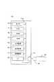
図1は本発明の一実施形態に係るメモリ装置100を接続可能なパーソナルコンピュータPCのハードウェア構成をメモリ装置100ともに示すブロック図、図2と図3はメモリ装置100を示す図、図4は表ケース12の内側の構造を示す斜視図、図5はプリント回路板20の実装面22aを示す平面図、図6はプリント回路板20に形成された回路を示す回路図である。(1) Configuration of memory device:
FIG. 1 is a block diagram showing a hardware configuration of a personal computer PC to which a
本発明を適用可能なメモリ装置は、コンピュータのインターフェイス用コネクタに接続可能なコネクタを外部に出してケースにメモリを収容したメモリ装置であればよく、汎用のUSB規格やシリアルSCSI(Serial Small Computer System Interface)規格等のシリアルインターフェイス規格のメモリ装置でもよいし、汎用のSCSI規格等のパラレルインターフェイス規格のメモリ装置でもよい。また、本メモリ装置は、コンパクトタイプの携帯可能な小型装置であると好適であり、ケースからケーブルを介してコネクタを有する装置でもよいが、ケースから直接コネクタが突出した装置であると好適である。さらに、本メモリ装置は、コンピュータから供給される電力で動作する装置であると、好適である。
本メモリ装置を接続可能なコンピュータには、パーソナルコンピュータやPDA(Personal Digital Assistant)等の端末等が用いられる。The memory device to which the present invention can be applied may be a memory device in which a connector that can be connected to an interface connector of a computer is provided outside and the memory is accommodated in a case, such as a general-purpose USB standard or serial SCSI (Serial Small Computer System). It may be a memory device of a serial interface standard such as an interface standard, or a memory device of a parallel interface standard such as a general-purpose SCSI standard. In addition, the memory device is preferably a compact and portable small device, and may be a device having a connector from the case via a cable, but is preferably a device in which the connector protrudes directly from the case. Further, the memory device is preferably a device that operates with power supplied from a computer.
A computer such as a personal computer or a PDA (Personal Digital Assistant) is used as a computer to which the memory device can be connected.
図1に示すように、PCでは、CPU P1、半導体メモリP2,P3、タイマ回路P4、ポインティングデバイスやキーボードといった入力装置P5、ディスプレイや音声出力装置といった出力装置P6、ハードディスクドライブや光ディスクドライブといった記憶装置P7、インターフェイス(I/F)P8、等が、所定のシステムバスP1aに接続され、互いに情報を入出力可能とされている。I/F P8には、メモリ装置のコネクタ30を嵌合可能なインターフェイス用コネクタP9が接続されている。タイマ回路P4は、現在の日時を計時する。CPU P1は、ROM P2に書き込まれた制御プログラムに従って、適宜、OS(Operating System)及びI/F制御プログラム等のアプリケーションプログラム(APL)並びに各種情報を記憶装置P7からRAM P3へ読み出して制御プログラムを実行する処理を行い、PC全体の動作を制御している。
I/F P8には、汎用のUSB規格やシリアルSCSI規格等のシリアルインターフェイス、汎用のSCSI規格等のパラレルインターフェイス、等を用いることができる。I/F P8にUSBインターフェイスが用いられる場合、コネクタP9にはUSB用のコネクタが用いられる。PCは、メモリ装置100からデータを読み出す時、データのアドレスを指定しながらデータの読み出し要求をメモリ装置100に出力する。なお、メモリ装置の製品開発時、すなわち、ケース10にプリント回路板20が収容されていない時、PCは、書き込むアドレスを指定しながらデータの書き込み要求をメモリ装置100に出力することにより、データをメモリ装置100に書き込むことができる。As shown in FIG. 1, in a PC, a CPU P1, semiconductor memories P2 and P3, a timer circuit P4, an input device P5 such as a pointing device and a keyboard, an output device P6 such as a display and an audio output device, and a storage device such as a hard disk drive and an optical disk drive P7, interface (I / F) P8, and the like are connected to a predetermined system bus P1a so that information can be input and output with each other. An interface connector P9 capable of fitting the
For the I / F P8, a serial interface such as a general-purpose USB standard or a serial SCSI standard, a parallel interface such as a general-purpose SCSI standard, or the like can be used. When a USB interface is used for the I / F P8, a USB connector is used for the connector P9. When reading data from the
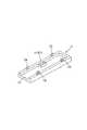
図3に示すように、メモリ装置100は、コネクタ30やメモリ40やコントロールIC52等を実装したプリント回路板20を表ケース12と裏ケース14とで挟み込んで形成される。ここで、メモリ40は、データを書き込み可能な不揮発性メモリとされ、ライトプロテクト信号(書き込みの可否を表す信号)を入力して該信号が書き込み不可の状態である時にデータを書き込み不可になる不揮発性メモリとされている。不揮発性メモリ40は、フラッシュメモリ等の半導体メモリが用いられ、例えば動画や音声やソフトウェア等のコンテンツ等が予め書き込まれる。図2に示すように表ケース12と裏ケース14とからなるケース10に不揮発性メモリ40が収容されている時、不揮発性メモリ40に入力されるライトプロテクト信号が書き込み不可の状態にされ、PCから不揮発性メモリ40にデータを書き込むことができない。従って、本メモリ装置100は、メモリ40に入力されるライトプロテクト信号が書き込み不可の状態にされてケース10に収容されているメモリ装置といえる。
また、本メモリ装置100は、メモリ40がケース10に収容される時にコンピュータPCからデータを書き込み不可にされたメモリ装置とされている。As shown in FIG. 3, the
The
表裏ケース12,14は、例えば、樹脂成形材料等を射出成形等により成形することにより、形成することができる。ケース10の材質は、絶縁材料が好ましい。むろん、プリント回路板20に形成される回路から絶縁されていれば、板金等の金属をプレス加工等により成形してケース10を形成してもよい。
図3と図4に示すように、ケース12,14は、プリント回路板20を収容するための溝12a,14aが形成されている。また、表ケース12には裏ケース14に向けて突出した係止用突起12bが複数形成され、裏ケース14には係止用穴14bが各突起12bに対応して形成されている。従って、各突起12bを各穴14bに挿入して裏ケース14に係止させると、表裏ケース12,14が互いに固定される。The front and
As shown in FIGS. 3 and 4, the
また、ケース10は、開状態(開いた状態)で不揮発性メモリ40を入れて閉じることによりプリント回路板20の被切断部24を切断する切断構造ST1を有している。この切断構造ST1は、プリント回路板の被切断部24の位置に合わせて表ケースの溝12aに形成した凹部13と、前記被切断部24の位置に合わせて裏ケースの溝14aに形成した凸部15とから構成されている。この凸部15は、凹部13よりも若干小さく形成されている。図5に示すように信号線25が被切断部24を通っているため、ケーシング時に切断構造ST1が信号線25を切断する。 The
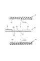
図5に示すように、プリント回路板20は、プリント基板とされた基板部22にコネクタ30や不揮発性メモリ40やコントロールIC52等の電子部品が実装されて形成されている。プリント回路板20に形成されたプリント回路は、コンピュータPCに対する信号の送受及び不揮発性メモリ40に対するデータの読み書きを制御する制御回路50を有している。また、プリント回路板20には、ケース10が閉じる動作をした時に制御回路50から物理的に切断される被切断部24が形成されている。図5に示す被切断部24は、プリント回路板20の下側縁部20aに形成され、該下側縁部からの切れ込みが予め左右の縁部に形成され、上側縁部24aが切断され易くされている。 As shown in FIG. 5, the printed
コネクタ30には、上述した汎用のUSB規格やシリアルSCSI規格等のシリアルインターフェイス、汎用のSCSI規格等のパラレルインターフェイス、等を用いることができる。コネクタ30は、コンピュータPC側のコネクタP9と嵌合して電気的に接続される。例えば、USB規格のコネクタでは、図6に示すように、電源端子V、グランド端子GND、信号端子D+,D−が設けられる。本メモリ装置100は、コネクタP9,30が接続されるとPCから通電され、コネクタ30のV端子に供給される電力をメモリ40や制御回路に供給する。 The
不揮発性メモリ40には、例えば、書き込みの可否を表すライトプロテクト信号(WP信号)を入力するライトプロテクト端子WPを有するフラッシュメモリを用いることができる。WP信号は、例えば、メモリ40への書き込み許可がH(High)レベルの電位で表され、メモリ40への書き込み不可がL(Low)レベルの電位で表される負論理の信号とされる。従って、メモリ40は、WP端子42がH(書き込み可の状態)である時にデータを書き込み可能になり、WP端子42がL(書き込み不可の状態)の状態であるときにデータを書き込み不可になる。むろん、メモリ40は、正論理のWP信号で動作するメモリ、すなわち、WP端子がLの状態である時に書き込み可能になり、WP端子がHの状態である時に書き込み不可になるメモリでもよい。この場合、WP信号には、メモリ40への書き込み不可がHで表される信号を使用すればよい。
メモリ40には、上記WP端子以外に、例えば、電源端子V、グランド端子GND、ライトイネーブル端子WE、リードイネーブル端子RE、アドレス端子An、データ端子Dn、等の端子を有する半導体メモリを用いることができる。As the
In addition to the WP terminal, for example, a semiconductor memory having terminals such as a power supply terminal V, a ground terminal GND, a write enable terminal WE, a read enable terminal RE, an address terminal An, and a data terminal Dn is used as the
制御回路50は、コントロールIC52及びその周辺回路から構成され、コネクタ30を介してコンピュータPCとデータを送受しながらメモリ40に対してデータの読み書きを行う。コントロールIC52には、例えば、コネクタ30の各端子V,GND,D+,D−に接続される端子V,GND,D+,D−、メモリ40の各端子WP,WE,RE,An,Dnに接続される端子WP,WE,RE,An,Dn、等の端子を有する半導体集積回路を用いることができる。ここで、コントロールICのWP端子54とメモリのWP端子42とを繋ぐWP信号線25は、図5に示す被切断部24を通り、該被切断部よりもメモリ40側で高抵抗R1の一端が接続されている。高抵抗R1の他端は、グランドラインGNDに接続されている。従って、信号線25が導通している時にはコントロールICのWP端子54の出力がメモリのWP端子42に入力され、信号線25が切断された時にはメモリのWP端子42の入力電位がLレベルになる。
なお、メモリのWP端子に接続されるコントロールICの端子は、信号出力用のI/O端子とされてもよい。The
Note that the terminal of the control IC connected to the WP terminal of the memory may be an I / O terminal for signal output.
コントロールIC52は、概略、図10に示すステップS102−S104の処理を行い、コンピュータPCと信号を送受しながらメモリ40からデータを読み出す。すなわち、コントロールIC52は、コネクタ30を介してコンピュータPCからデータの読み出し要求を入力すると、WP端子54からLレベルのWP信号を出力しながら前記読み出し要求に含まれるアドレスのデータをメモリ40から読み出し、該データを信号端子からPCに対して出力する。また、プリント回路板20がケース10に収容される前には図10に示すステップS106,S110の処理を行い、コンピュータPCと信号を送受しながらメモリ40にデータを書き込むことが可能である。すなわち、コントロールIC52は、コネクタ30を介してコンピュータPCからデータの書き込み要求を入力すると、WP端子54からHレベルのWP信号を出力しながら前記書き込み要求に含まれるアドレスに対して該書き込み要求に含まれるデータを書き込む。なお、コントロールIC52には、論理回路を組み合わせた集積回路を用いることができ、CPUやROMやRAMを有するマイコンを用いてもよい。 The
(2)メモリ装置の製造方法並びに作用及び効果:
図3と図7は、メモリ装置100を製造する様子を示している。
メモリ装置100を製造するには、まず、表裏の各ケース12,14を形成し、不揮発性メモリ40を実装し制御回路50を形成したプリント回路板20を形成する。次に、プリント回路板20の裏面22bを裏ケース14に向けてプリント回路板20を裏ケースの溝14aに入れ、プリント回路板の実装面22a側を表ケースの溝12aに入れて、開状態のケース10を閉じていく。そして、各係止用突起12bが各係止用穴14bに挿入して裏ケース14に係止すると、表裏ケース12,14が互いに固定され、ケース10内の収容空間SP1にプリント回路板20が収容されて、メモリ装置100が形成される。このときの状態が、図2の斜視図と図8の垂直断面図に示されている。(2) Memory device manufacturing method, operation and effect:
3 and 7 show how the
To manufacture the
ここで、ケース10に切断構造13,15が形成されているので、図8に示すように、裏ケースの凸部15が被切断部24を凹部13内に押し込んで切断する。すなわち、プリント回路板を入れたケース10が閉じる動作をした時にWP信号線25が切断され、メモリのWP端子42に入力されるWP信号が常時Lレベル(書き込み不可の状態)にされる。これにより、不揮発性メモリ40は、コンピュータPCからデータを書き込み不可とされる。
以上より、本発明には、メモリにデータを書き込み可能な不揮発性メモリを用い、該不揮発性メモリをケースに収容する時にコンピュータから該不揮発性メモリへデータを書き込むことができないようにしてメモリ装置を製造するメモリ装置の製造方法が含まれる。また、本発明には、メモリがデータを書き込み可能な不揮発性メモリとされ、該不揮発性メモリがケースに収容される時にコンピュータからデータを書き込み不可にされたメモリ装置が含まれる。Here, since the cutting
As described above, the present invention uses a nonvolatile memory capable of writing data to the memory, and prevents the memory device from being written to the nonvolatile memory when the nonvolatile memory is accommodated in the case. A method of manufacturing a memory device to be manufactured is included. Further, the present invention includes a memory device in which the memory is a nonvolatile memory into which data can be written, and data cannot be written from a computer when the nonvolatile memory is accommodated in a case.
不揮発性メモリがケースに収容されている状態でコンピュータからデータを書き込み不可にされているので、メモリ装置のユーザがコンテンツ等の情報を書き換えることができない。また、ケースに不揮発性メモリが収容される前にはコンピュータからデータを書き込み可能であるので、不揮発性メモリにデータが容易に記録され、メモリ装置の製品開発時と製造時とでプリント回路板を別々に設計する必要が無い。従って、ユーザ側でメモリの情報を書き換えることができないようにしたメモリ装置を安価に製造することができる。
また、ケースを閉じるだけで信号線が切断されるので、容易にコンピュータから不揮発性メモリへのデータの書き込みを不可能にさせることができる。従って、メモリ装置の製造コストをさらに低減させることができる。Since data cannot be written from the computer while the nonvolatile memory is housed in the case, the user of the memory device cannot rewrite information such as contents. In addition, since data can be written from a computer before the nonvolatile memory is accommodated in the case, the data can be easily recorded in the nonvolatile memory, and the printed circuit board can be used at the time of product development and manufacturing of the memory device. There is no need to design separately. Therefore, it is possible to manufacture a memory device that prevents the user from rewriting memory information at low cost.
Further, since the signal line is disconnected simply by closing the case, it is possible to easily make it impossible to write data from the computer to the nonvolatile memory. Therefore, the manufacturing cost of the memory device can be further reduced.
さらに、切断された被切断部24が表ケースの凹部13内に隔離されるので、ケース10内に被切断部24が残されても問題が生じない。加えて、被切断部24があった部分に凸部15が入るので、プリント回路板20が凸部15で位置決めされて固定される利点もある。なお、上述したような凸部を表ケースに形成して上述したような凹部を裏ケースに形成しても同様の作用、効果が得られるが、裏ケース14に凸部15を形成し表ケース12に凹部13を形成するとケース10内の狭い空間を有効利用することができる点で好適である。 Furthermore, since the
(3)変形例:
コンピュータから不揮発性メモリがデータを書き込み不可にされることには、メモリ装置内の制御回路がコンピュータからのデータの書き込みを禁止しながら不揮発性メモリのデータを書き換え可能であることも含まれる。
図9−図11には、一定の条件が成立した時にコントロールIC52が不揮発性メモリ40のデータを消す処理を行うメモリ装置を示している。本変形例の制御回路(データ消去手段)50は、本メモリ装置の使用状況を表す情報に基づいて不揮発性メモリのデータを消す条件が成立したか否かを判断し、条件成立時にWP信号を書き込み可の状態にして不揮発性メモリ40のデータを消す。これにより、メモリ装置の使用状況に応じて情報が消去されるので、情報を書き換え不可にしたメモリ装置の利便性を向上させることができる。(3) Modification:
Making the nonvolatile memory incapable of writing data from the computer includes that the control circuit in the memory device can rewrite the data in the nonvolatile memory while prohibiting writing of data from the computer.
9 to 11 show a memory device in which the
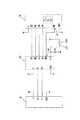
本コントロールIC52は、信号入力用のI/O端子を有する集積回路(マイコンを含む)とされている。このI/O端子は、信号線26でグランドに接続されている。信号線26は、被切断部24を通り、該被切断部よりもI/O端子側で高抵抗R2の一端が接続されている。高抵抗R2の他端は、電源ラインVに接続されている。従って、信号線26が導通している時にはI/O端子の入力電位がLレベルとなり、信号線26が切断された時にはI/O端子の入力電位がHレベルになる。一方、コントロールICのWP端子54とメモリのWP端子42とは、被切断部24を通らないWP信号線25で接続されている。不揮発性メモリのデータを消す条件が成立していない時、コントロールIC52は、WP端子54から常時Lレベル(書き込み不可の状態)のWP信号を出力する。また、不揮発性メモリ40は、フラッシュメモリ等の半導体メモリとされ、メモリ40のデータを消す日時を表す情報(有効期限Ts)が記憶されている。
一方、コンピュータPCは、メモリ装置100から日時情報の出力要求を入手した時にタイマ回路P4から現在の日時を表す情報Tnを入手してメモリ装置100に対して出力する機能を有するものとする。The
On the other hand, the computer PC has a function of obtaining information Tn indicating the current date and time from the timer circuit P4 and outputting the information to the
コントロールIC52は、図10に示すメモリ管理処理をメモリ装置の製品開発時及び生産時に行う。本処理は、コンピュータからメモリ装置に電力が供給されている間、繰り返し行われる。
処理を開始すると、コントロールIC52は、まず、コネクタ30を介してコンピュータPCからデータの読み出し要求が入力されたか否かを判断する(ステップS102。以下、「ステップ」の記載を省略)。条件不成立時、S106に進む。条件成立時、WP端子54からLレベル(書き込み不可の状態)のWP信号を出力しながら前記読み出し要求に含まれるアドレスのデータをメモリ40から読み出し、該データを信号端子からPCに対して出力する(S104)。The
When the process is started, the
S106では、コネクタ30を介してコンピュータPCからデータの書き込み要求が入力されたか否かを判断する。条件不成立時、本処理を終了する。条件成立時、I/O端子の入力電位がHレベル(切断状態)か否かを判断する(S108)。被切断部24が切断されていない製品開発時には信号線26が導通してI/O端子がLレベルとなっているため、S110でWP端子54からHレベル(書き込み可の状態)のWP信号を出力しながら前記書き込み要求に含まれるアドレスに対して該書き込み要求に含まれるデータを書き込み、本処理を終了する。一方、被切断部24が切断された生産後には信号線26が切断されてI/O端子がHレベルとなっているため、S110の処理を行わずに本処理を終了する。
以上より、メモリ装置のユーザ側は不揮発性メモリに書き込まれた情報を書き換えることができない。
なお、信号線26が導通している時にI/O端子の入力電位がHレベルとされ、信号線26が切断された時にI/O端子の入力電位がLレベルとされてもよい。この場合、S108ではI/O端子の入力電位がLレベルか否かを判断すればよい。In S <b> 106, it is determined whether a data write request is input from the computer PC via the
As described above, the user side of the memory device cannot rewrite information written in the nonvolatile memory.
Note that the input potential of the I / O terminal may be H level when the
また、コントロールIC52は、図11に示すように、現在の日付及び時刻を表す日時情報(メモリ装置の使用状況を表す情報)Tnに基づいて不揮発性メモリのデータを消す条件成立の可否を判断する。同図に示す有効期限管理処理は、コンピュータからメモリ装置に電力が供給されている間、上記メモリ管理処理と並列して繰り返し行われる。
処理を開始すると、コントロールIC52は、まず、PCに対して日時情報の出力要求を出力し、PCから現在の日時を表す情報Tnを入手する(S202)。次に、メモリ40から有効期限Tsを読み出す(S204)。むろん、S204の処理はS202の処理前に行われてもよい。そして、両情報Tn,Tsを対比し、現在の日時Tnが有効期限Tsを過ぎたか否かを判断する(S206)。なお、Tn,Tsを日時が後になるほど大きくなる数値情報にすると、Tn>Tsであるか否かを判断すればよい。現在の日時Tnが有効期限Tsを過ぎていない場合、不揮発性メモリのデータを消す条件が成立していないため、本処理を終了する。一方、現在の日時Tnが有効期限Tsを過ぎた場合、不揮発性メモリのデータを消す条件が成立したことになり、Lレベル(書き込み不可の状態)であったWP端子54からHレベル(書き込み可の状態)のWP信号を出力し、この状態で不揮発性メモリ40に記憶されているデータを消去し(S208)、本処理を終了する。Further, as shown in FIG. 11, the
When the process is started, the
不揮発性メモリに書き込まれる情報には、著作権等の関係で有効期限を設定したい情報もある。本メモリ装置では、このような情報が不揮発性メモリに書き込まれても有効期限Ts後に消去されるので、利便性が向上する。 Information written to the nonvolatile memory includes information for which an expiration date is desired to be set due to copyrights and the like. In the present memory device, even if such information is written in the nonvolatile memory, it is deleted after the expiration date Ts, so that convenience is improved.
なお、コントロールICがPCに対して日時情報の出力要求を出力する機能を有していない場合、メモリ装置を接続したPCが一定時間毎に現在の日時Tnをメモリ装置に対して出力すれば、コントロールICはPCから現在の日時Tnが入力された時点で有効期限管理処理を開始して有効期限後に不揮発性メモリのデータを消去することができる。
また、PCから現在の日時Tnを入手すればメモリ装置にタイマ回路を設けなくてよい点で好適であるものの、メモリ装置にタイマ回路を設けて該タイマ回路から現在の日時Tnを入手して有効期限管理処理を行ってもよい。If the control IC does not have a function of outputting a date / time information output request to the PC, if the PC connected to the memory device outputs the current date / time Tn to the memory device at regular intervals, The control IC can start the expiration date management process when the current date and time Tn is input from the PC and can erase the data in the nonvolatile memory after the expiration date.
In addition, it is preferable that the current date and time Tn is obtained from the PC because it is not necessary to provide a timer circuit in the memory device. However, it is effective to obtain a current date and time Tn from the timer circuit by providing a timer circuit in the memory device. You may perform a term management process.
さらに、不揮発性メモリに有効期限Tsを書き込むと有効期限Tsの違いによってコントロールICを別々に用意しなくてよい点で好適であるものの、コントロールICに有効期限Tsを保持させて該有効期限Tsを読み出して有効期限管理処理を行ってもよい。
さらに、情報Tn,Tsは、年月日及び時刻の少なくとも一部を表す情報であればよく、年を表す年情報でも、月を表す月情報でも、日付を表す日付情報でも、時刻を表す時刻情報でも、これらを組み合わせた情報でもよい。Furthermore, although writing the expiration date Ts in the non-volatile memory is preferable in that it is not necessary to prepare a separate control IC depending on the difference in the expiration date Ts, the control IC holds the expiration date Ts and sets the expiration date Ts. You may read and perform an expiration date management process.
Further, the information Tn, Ts may be information representing at least a part of the year, month, day, and time. The time representing the time, whether the year information representing the year, the month information representing the month, or the date information representing the date. Information or a combination of these may be used.
さらに、現在の年月日及び時刻の少なくとも一部を表す情報Tnと不揮発性メモリのデータを消す年月日及び時刻の少なくとも一部を表す情報Tsとを対比してデータを消す条件成立の可否を判断する以外にも、メモリ装置への通電時間Teを計測し該通電時間Teに基づいてデータを消す条件成立の可否を判断してもよい。 Further, whether or not a condition for erasing data is established by comparing information Tn representing at least part of the current date and time with information Ts representing at least part of the date and time of erasing data in the nonvolatile memory. In addition to determining whether or not the condition for erasing data is measured based on the energization time Te of the memory device and data is erased may be determined.
また、図12に示す変形例は、本メモリ装置の使用状況を表す情報として本メモリ装置に通電された回数Ceを用いる有効回数管理処理を示している。コントロールIC52は、メモリ装置100への通電が開始された時に本処理を行う。なお、図9に示す回路がプリント回路板20に形成され、図10に示すメモリ管理処理がコントロールIC52で繰り返し行われるものとする。また、不揮発性メモリ40は、フラッシュメモリ等の半導体メモリとされ、メモリ40のデータを消す通電回数を表す情報(図9に示す有効回数Cs)を記憶しているものとする。さらに、不揮発性メモリ40は、通電回数を表すカウンタCeを有し、ケース10にプリント回路板20が収容された時点でカウンタCeが0にされているものとする。 Further, the modification shown in FIG. 12 shows the effective number management process using the number Ce of energization of the memory device as information indicating the usage status of the memory device. The
処理を開始すると、コントロールIC52は、まず、WP端子54からHレベル(書き込み可の状態)のWP信号を出力し、この状態でカウンタCeの値を1だけ増加させる(S302)。これにより、本メモリ装置に通電された回数Ceがカウントされる。その後、WP端子54からLレベル(書き込み不可の状態)のWP信号を出力しておく。次に、メモリ40から有効回数Csを読み出す(S304)。むろん、S304の処理はS302の処理前に行われてもよい。そして、両情報Ce,Csを対比し、現在の通電回数Ceが有効回数Csを超えたか否かを判断する(S306)。現在の通電回数Ceが有効回数Csを超えていない場合、不揮発性メモリのデータを消す条件が成立していないため、本処理を終了する。一方、現在の通電回数Ceが有効回数Csを超えた場合、不揮発性メモリのデータを消す条件が成立したことになり、Lレベル(書き込み不可の状態)であったWP端子54からHレベル(書き込み可の状態)のWP信号を出力し、この状態で不揮発性メモリ40に記憶されているデータを消去し(S308)、本処理を終了する。 When the process is started, the
不揮発性メモリに書き込まれる情報には、著作権等の関係で有効な通電回数を設定したい情報もある。本メモリ装置では、このような情報が不揮発性メモリに書き込まれても有効回数Cs後に消去されるので、利便性が向上する。 Some information written in the non-volatile memory includes information for which an effective number of energizations is to be set due to copyrights and the like. In this memory device, even if such information is written in the nonvolatile memory, the information is erased after the effective number of times Cs, so that convenience is improved.
上述した各種の実施形態において、プリント回路板に被切断部24を設ける代わりに、図13に示すようなワイヤ125をプリント回路板120に設けてもよい。本プリント回路板120に形成されたプリント回路は、コンピュータPCに対する信号の送受及び不揮発性メモリ40に対するデータの読み書きを制御する制御回路150を有している。また、プリント回路板120の下側縁部20aには、上記被切断部24に相当する位置に切欠124が形成されている。この切欠124には、ケース10が閉じる動作をした時に裏ケースの凸部15が挿入される。ここで、コントロールIC52のWP端子54とメモリのWP端子42とを繋ぐWP信号線の一部がワイヤ125とされ、このワイヤ125の両端が切欠124を跨いで基板部22に接続されている。このワイヤ125は、ケース10が閉じる動作をした時に切断機構13,15で切断されるようにされている。 In the various embodiments described above, a
開状態の表裏ケース12,14にメモリ40を入れて両ケース12,14を閉じると、裏ケースの凸部15がワイヤ125の一部を凹部13内に押し込んで切断する。すなわち、プリント回路板を入れたケース10が閉じる動作をした時にWP信号線が切断され、メモリのWP端子42に入力されるWP信号が常時Lレベル(書き込み不可の状態)にされる。これにより、不揮発性メモリ40は、コンピュータPCからデータを書き込み不可とされる。
このように、ケースを閉じるだけで信号線が切断されるので、容易にコンピュータから不揮発性メモリへのデータの書き込みを不可能にさせることができる。従って、ユーザ側でメモリの情報を書き換えることができないようにしたメモリ装置を安価に製造することができる。When the
As described above, since the signal line is disconnected only by closing the case, it is possible to easily make it impossible to write data from the computer to the nonvolatile memory. Therefore, it is possible to manufacture a memory device that prevents the user from rewriting memory information at low cost.
また、上記被切断部24や上記ワイヤ125を切断する処理を行った後にケースを閉じても、入力されるWP信号が書き込み不可の状態にされて不揮発性メモリがケースに収容されているメモリ装置が形成される。
さらに、不揮発性メモリにデータを書き込む時には切断されている信号線を導電性の治具で挟んで導電させておき、ケーシング時に治具を外して信号線を断ち切ることによりWP信号を常時書き込み不可の状態にしてもよい。Further, even if the case is closed after performing the process of cutting the
Furthermore, when writing data to the non-volatile memory, the signal line that has been cut is made conductive by sandwiching it with a conductive jig, and the WP signal cannot be written at all times by removing the jig when the casing is cut and cutting the signal line. It may be in a state.
さらに、図14−図16に示すメモリ装置300のように、ケーシング時に信号線を導通させる導通構造213をケース210に設けてもよい。本変形例のプリント回路板220には、上記被切断部24に相当する位置にプッシュスイッチ224が実装されている。一方、表ケース212には、開状態で半導体メモリ40を入れて閉じることにより信号線225を導通させる導通構造213を有している。この導通構造213は、プリント回路板のスイッチ224の位置に合わせて表ケース212の溝12aに形成した凸部とされている。なお、裏ケース214に上記凸部15は形成されていない。 Further, as in the
コントロールIC52のI/O端子は、スイッチ224を介して信号線225でグランドに接続されている。信号線225は、スイッチ224よりもI/O端子側で高抵抗R3の一端が接続されている。高抵抗R3の他端は、グランドに接続されている。従って、スイッチ224が押されず信号線225が導通していない時にはI/O端子の入力電位がLレベルとなり、スイッチ224が押され信号線225が導通した時にはI/O端子の入力電位がHレベルになる。コントロールIC52は、I/O端子の入力電位がLレベル(スイッチオフ状態)の時にはWP端子54から出力するWP信号を適宜Lレベル又はHレベルに切り替え、I/O端子の入力電位がHレベル(スイッチオン状態)の時にはメモリ40のデータを消す条件が成立しない限りWP端子54から常時Lレベル(書き込み不可の状態)のWP信号を出力する。
なお、有効期限Tsを過ぎたり有効回数Csを超えたりした時にメモリ40のデータを消す場合には、図11で示した有効期限管理処理や図12で示した有効回数管理処理をコントロールIC52で行えばよい。The I / O terminal of the
When the data in the
本変形例では、ケースを閉じるだけで信号線が導通してWP信号が書き込み不可の状態になるので、容易にコンピュータから不揮発性メモリへのデータの書き込みを不可能にさせることができる。従って、ユーザ側でメモリの情報を書き換えることができないようにしたメモリ装置を安価に製造することができる。
なお、プリント回路板220の裏面22bにプッシュスイッチを設けて裏ケース214に導通機構を設けても同様の作用、効果が得られるが、プリント回路板220の実装面22aにプッシュスイッチを設けて表ケース212に導通機構を設けるとケース210内の狭い空間を有効利用することができる点で好適である。In the present modification, the signal line becomes conductive and the WP signal cannot be written by simply closing the case, so that it is easy to make it impossible to write data from the computer to the nonvolatile memory. Therefore, it is possible to manufacture a memory device that prevents the user from rewriting memory information at low cost.
Although the same operation and effect can be obtained by providing a push switch on the
また、上記凸部213の代わりに導電スポンジといった導電体を表ケース212の溝12aに取り付け、切断されている信号線をケーシング時に導電体で導電させてWP信号を書き込み不可の状態にしてもよい。
さらに、信号線を導通させる処理を行った後にケースを閉じても、入力されるWP信号が書き込み不可の状態にされて不揮発性メモリがケースに収容されているメモリ装置が形成される。Alternatively, a conductor such as a conductive sponge may be attached to the
Further, even if the case is closed after conducting the process of making the signal line conductive, the input WP signal is made unwritable and a memory device in which the nonvolatile memory is accommodated in the case is formed.
上述した各種の実施形態において、分離された表裏ケースからなるケースを用いる代わりに、表部分と裏部分とが開閉可能に繋がったケースを用いてもよい。このようなケースには、表部分と裏部分とがヒンジ機構で一体的に繋がったケース等が考えられる。
上述した各種の実施形態において、不揮発性メモリに入力されるWP信号が書き込み不可の状態にされて不揮発性メモリがコンピュータからデータを書き込み不可にされる以外にも、例えば、不揮発性メモリに入力されるライトイネーブル信号WEが書き込み不可の状態にされて不揮発性メモリがコンピュータからデータを書き込み不可にされてもよい。後者の場合、WE信号が書き込みの可否を表す信号となる。In the various embodiments described above, a case in which the front portion and the back portion are connected so as to be openable and closable may be used instead of using a case composed of the separated front and back cases. As such a case, a case in which a front portion and a back portion are integrally connected by a hinge mechanism is conceivable.
In the various embodiments described above, in addition to the WP signal input to the nonvolatile memory being made unwritable and the nonvolatile memory being made unwritable by the computer, for example, the WP signal is inputted to the nonvolatile memory. The write enable signal WE may be disabled, and the nonvolatile memory may be disabled to write data from the computer. In the latter case, the WE signal is a signal indicating whether or not writing is possible.
上述した被切断部24、ワイヤ125、プッシュスイッチ224は、プリント回路上で不揮発性メモリ40とコントロールIC52との間に設けられる以外にも、コントロールIC52とコネクタ30との間に設けられてもよい。
図17は被切断部324をコントロールIC52とコネクタ30との間に形成したプリント回路板320を示す平面図であり、図18はプリント回路板320に形成された回路を示す回路図である。被切断部324は、上述した被切断部24と同様、プリント回路板320の下側縁部20aからの切れ込みが予め左右の縁部に形成され、上側縁部324aが切断され易くされている。コントロールIC52のI/O端子は、信号線324でグランドに接続されている。信号線325は、被切断部324を通り、該被切断部よりもI/O端子側で高抵抗R4の一端が接続されている。高抵抗R4の他端は、電源ラインVに接続されている。また、コントロールICのWP端子(又は出力用のI/O端子)54とメモリのWP端子42とは、被切断部324を通らないWP信号線で接続されている。The
FIG. 17 is a plan view showing a printed
被切断部324が切断されていない製品開発時には信号線325が導通してI/O端子の入力電位がLレベルとなり、WP端子54からHレベル(書き込み可の状態)のWP信号を出力して不揮発性メモリ40へのデータの書き込みを可能にする。一方、被切断部324が切断された生産後には信号線325が切断されてI/O端子の入力電位がHレベルとなり、WP端子54からLレベル(書き込み不可の状態)のWP信号を出力して不揮発性メモリ40へのデータの書き込みを不可能にする。これにより、不揮発性メモリがケースに収容されている状態でコンピュータからデータを書き込み不可にされるので、安価にてユーザ側でコンテンツ等の情報を書き換えることができないようにすることができる。 When developing the product in which the
なお、本発明は、上述した実施形態や変形例に限られず、上述した実施形態及び変形例の中で開示した各構成を相互に置換したり組み合わせを変更したりした構成、公知技術並びに上述した実施形態及び変形例の中で開示した各構成を相互に置換したり組み合わせを変更したりした構成、等も含まれる。 Note that the present invention is not limited to the above-described embodiments and modifications, and the configurations disclosed in the above-described embodiments and modifications are mutually replaced or the combination is changed, the known technology, and the above-described configurations. Configurations in which the respective configurations disclosed in the embodiment and the modified examples are mutually replaced or combinations are changed are also included.
10,210…ケース、
12…表ケース、12a…溝、12b…係止用突起、13…凹部、
14…裏ケース、14a…溝、14b…係止用穴、15…凸部、
20,120,220,320…プリント回路板、
22…基板部、22a…実装面、
24,324…被切断部、25,26,325…信号線、
30…コネクタ、
40…フラッシュメモリ(不揮発性メモリ)、
42…ライトプロテクト端子、
50…制御回路(データ消去手段)、
52…コントロールIC、54…ライトプロテクト端子、
100,300…メモリ装置、
124…切欠、125…ワイヤ、
213…凸部(導通構造)、224…プッシュスイッチ、
P8…インターフェイス、P9…インターフェイス用コネクタ、
PC…コンピュータ、
SP1…収容空間、ST1…切断構造、10, 210 ... case,
12 ... front case, 12a ... groove, 12b ... locking projection, 13 ... recess,
14 ... Back case, 14a ... Groove, 14b ... Locking hole, 15 ... Projection,
20, 120, 220, 320 ... printed circuit board,
22 ... Board part, 22a ... Mounting surface,
24, 324 ... cut parts, 25, 26, 325 ... signal lines,
30 ... Connector,
40: Flash memory (nonvolatile memory),
42: Write protect terminal,
50... Control circuit (data erasing means)
52 ... Control IC, 54 ... Write protect terminal,
100, 300 ... Memory device,
124 ... notch, 125 ... wire,
213 ... convex part (conduction structure), 224 ... push switch,
P8 ... interface, P9 ... interface connector,
PC ... computer,
SP1 ... accommodating space, ST1 ... cutting structure,
Claims (8)
Translated fromJapanese前記メモリは、データを書き込み可能であるとともに書き込みの可否を表す信号を入力して該信号が書き込み不可の状態である時にデータを書き込み不可になる不揮発性メモリとされ、
前記ケースは、開いて前記不揮発性メモリを入れた状態から閉じることにより前記書き込みの可否を表す信号が書き込み可の状態から書き込み不可の状態になる構造を有し、
前記不揮発性メモリは、入力される前記書き込みの可否を表す信号が前記構造により書き込み不可の状態にされて前記ケースに収容されていることを特徴とするメモリ装置。A memory device in which a connector that can be connected to an interface connector of a computer is taken out and a memory is accommodated in a case,
The memory is a non-volatile memory in which data is writable and a signal indicating whether data can be written is input and data is not writable when the signal is in a writable state.
The case has a structure in which a signal indicating whether the writing is possible or not can be changed from a writable state to a non-writable state by closing from a state where the nonvolatile memory is opened.
The non-volatile memory is a memory device characterized in that an input signal indicating whether or not writing is possible is made in a state in which writing is impossibleby the structure and is housed in the case.
前記データ消去手段は、前記コンピュータから現在の年月日及び時刻の少なくとも一部を表す情報を入手し、該情報に基づいて前記不揮発性メモリのデータを消す条件が成立したか否かを判断して条件成立時に前記信号を書き込み可の状態にして前記不揮発性メモリのデータを消すことを特徴とする請求項2に記載のメモリ装置。The information representing the usage status is information representing at least part of the current date and time,
The data erasing means obtains information representing at least a part of the current date and time from the computer, and determines whether or not a condition for erasing data in the nonvolatile memory is satisfied based on the information.3. The memory device according toclaim 2 , wherein when the condition is satisfied, the signal is made writable and data in the nonvolatile memory is erased.
前記データ消去手段は、本メモリ装置に通電された回数をカウントし、前記不揮発性メモリのデータを消す通電回数と前記カウントした回数とを対比して前記不揮発性メモリのデータを消す条件が成立したか否かを判断して条件成立時に前記信号を書き込み可の状態にして前記不揮発性メモリのデータを消すことを特徴とする請求項2に記載のメモリ装置。The information indicating the usage status is the number of times the memory device is energized,
The data erasing means counts the number of times the memory device is energized, and the condition for erasing the data in the nonvolatile memory is established by comparing the number of energizations to erase the data in the nonvolatile memory and the counted number.3. The memory device according toclaim 2 , wherein when the condition is satisfied, the signal is made writable and data in the nonvolatile memory is erased. 4.
前記ケースの構造は、開いた状態で前記半導体メモリを入れて閉じることにより信号線を切断する構造とされ、
前記半導体メモリを入れた前記ケースが閉じる動作をした時に前記信号線が切断されて前記端子に入力される信号が書き込み不可の状態にされたことを特徴とする請求項1〜請求項4のいずれか一項に記載のメモリ装置。The nonvolatile memory is a semiconductor memory that has a terminal for inputting a signal indicating whether the writing is possible and cannot write data when the signal is in a non-writable state.
Structure of the caseis a structure in the opened state to cut the signal line by closing put the semiconductor memory,
5. The signal input to the terminal is made unwritable by cutting the signal line when the case containing the semiconductor memory is closed.5 . A memory device according to claim 1.
前記ケースの構造は、開いた状態で前記半導体メモリを入れて閉じることにより信号線を導通させる構造とされ、
前記半導体メモリを入れた前記ケースが閉じる動作をした時に前記信号線が導通して前記端子に入力される信号が書き込み不可の状態にされたことを特徴とする請求項1〜請求項4のいずれか一項に記載のメモリ装置。The nonvolatile memory is a semiconductor memory that has a terminal for inputting a signal indicating whether the writing is possible and cannot write data when the signal is in a non-writable state.
Structure of the caseis a structure for conducting the signal line by in a state of open close putting the semiconductor memory,
5. The signal according toclaim 1 , wherein when the case containing the semiconductor memory is closed, the signal line is turned on and a signal input to the terminal cannot be written. A memory device according to claim 1.
前記メモリを実装したプリント回路板が前記ケースに収容されるとともに、前記コネクタを介して前記コンピュータとデータを送受しながら前記メモリに対してデータの読み書きを行う制御回路が前記プリント回路板に形成され、
前記メモリは、書き込みの可否を表すライトプロテクト信号を入力するライトプロテクト端子を有して該ライトプロテクト信号が書き込み不可の状態である時にデータを書き込み不可になるフラッシュメモリとされ、
前記ケースは、前記フラッシュメモリを実装し前記制御回路を形成したプリント回路板を入れて開状態から閉じることにより該プリント回路板を収容し信号線を切断する構造を有し、
前記プリント回路板を入れた前記ケースが閉じる動作をした時に前記信号線が切断されて前記ライトプロテクト端子に入力される信号が書き込み可の状態から書き込み不可の状態にされることにより前記フラッシュメモリが前記コンピュータからデータを書き込み不可にされ、
前記制御回路は、前記コンピュータから現在の年月日及び時刻の少なくとも一部を表す情報を入手し、該情報に基づいて前記フラッシュメモリのデータを消す条件が成立したか否かを判断して条件成立時に前記ライトプロテクト信号を書き込み可の状態にして前記フラッシュメモリのデータを消すことを特徴とするメモリ装置。A memory device in which a connector that can be connected to an interface connector of a computer is taken out and a memory is accommodated in a case,
A printed circuit board on which the memory is mounted is housed in the case, and a control circuit that reads / writes data from / to the memory while sending / receiving data to / from the computer via the connector is formed on the printed circuit board. ,
The memory has a write protect terminal for inputting a write protect signal indicating whether or not writing is possible, and is a flash memory in which data cannot be written when the write protect signal is in a write disable state.
The case has a structure for receiving the printed circuit board and cutting the signal line by closing the open circuit state by inserting a printed circuit board on which the flash memory is mounted and forming the control circuit.
When the case in which the printed circuit board is inserted is closed, the signal line is cut and the signal input to the write protect terminal ischanged from a writablestate to a non-writable state. Data is not writable from the computer,
The control circuit obtains information representing at least a part of the current date and time from the computer, and determines whether or not a condition for erasing the data in the flash memory is satisfied based on the information. A memory device characterized in that, when established, the write protect signal is set in a writable state to erase data in the flash memory.
前記メモリにデータを書き込み可能であるとともに書き込みの可否を表す信号を入力して該信号が書き込み不可の状態である時にデータを書き込み不可になる不揮発性メモリを用い、開いて前記不揮発性メモリを入れた前記ケースを閉じることにより前記不揮発性メモリに入力する前記書き込みの可否を表す信号を書き込み可の状態から書き込み不可の状態にしてメモリ装置を製造することを特徴とするメモリ装置の製造方法。A method of manufacturing a memory device in which a connector that can be connected to an interface connector of a computer is provided outside and a memory is accommodated in a case,
Use a non-volatile memory that can write data to the memory and input a signal indicating whether or not data can be written and cannot write data when the signal is not writable, andopen the non-volatile memory. a method of manufacturing the memory device characterized by manufacturing amemory deviceandthe state of the enable write a signal to the state of non-writable representing whether or not said write input tothe non-volatile memoryby closing the case was.
Priority Applications (1)
| Application Number | Priority Date | Filing Date | Title |
|---|---|---|---|
| JP2007068312AJP5080833B2 (en) | 2007-03-16 | 2007-03-16 | Memory device and manufacturing method thereof |
Applications Claiming Priority (1)
| Application Number | Priority Date | Filing Date | Title |
|---|---|---|---|
| JP2007068312AJP5080833B2 (en) | 2007-03-16 | 2007-03-16 | Memory device and manufacturing method thereof |
Publications (2)
| Publication Number | Publication Date |
|---|---|
| JP2008233972A JP2008233972A (en) | 2008-10-02 |
| JP5080833B2true JP5080833B2 (en) | 2012-11-21 |
Family
ID=39906724
Family Applications (1)
| Application Number | Title | Priority Date | Filing Date |
|---|---|---|---|
| JP2007068312AExpired - Fee RelatedJP5080833B2 (en) | 2007-03-16 | 2007-03-16 | Memory device and manufacturing method thereof |
Country Status (1)
| Country | Link |
|---|---|
| JP (1) | JP5080833B2 (en) |
Families Citing this family (4)
| Publication number | Priority date | Publication date | Assignee | Title |
|---|---|---|---|---|
| JP5297761B2 (en)* | 2008-10-28 | 2013-09-25 | 株式会社ワイ・イー・データ | Write prevention adapter device for USB memory |
| JP6619269B2 (en)* | 2016-03-22 | 2019-12-11 | キオクシア株式会社 | USB device and manufacturing method thereof |
| CN106779025B (en)* | 2016-12-09 | 2024-04-19 | 杭州佩安科技有限公司 | Novel nonvolatile anti-rewriting memory |
| CN112823351B (en)* | 2018-10-12 | 2024-06-25 | 里米奇公司 | Automatic storage unit publisher |
Family Cites Families (4)
| Publication number | Priority date | Publication date | Assignee | Title |
|---|---|---|---|---|
| JPS62108099A (en)* | 1985-11-06 | 1987-05-19 | 富士通株式会社 | Integrated circuit card |
| JPH05314011A (en)* | 1992-05-08 | 1993-11-26 | Sharp Corp | Ic card |
| JP3689213B2 (en)* | 1997-01-21 | 2005-08-31 | ローム株式会社 | Non-contact IC card |
| JP2006018499A (en)* | 2004-06-30 | 2006-01-19 | Sony Corp | Data storage device, data providing system, and data providing method |
- 2007
- 2007-03-16JPJP2007068312Apatent/JP5080833B2/ennot_activeExpired - Fee Related
Also Published As
| Publication number | Publication date |
|---|---|
| JP2008233972A (en) | 2008-10-02 |
Similar Documents
| Publication | Publication Date | Title |
|---|---|---|
| US6754548B1 (en) | Reproducing device having reproducing limiting function, apparatus for rewriting reproducing limitation information, reproducing limiting method, method of rewriting reproducing limitation information and program storage medium | |
| US7443690B2 (en) | Adapter device, memory device and integrated circuit chip | |
| US7062585B2 (en) | Memory card for integrating the USB interface and an adaptor for the memory card | |
| JP5080833B2 (en) | Memory device and manufacturing method thereof | |
| US6786417B1 (en) | Memory card with write protection switch | |
| JP2004213574A (en) | Data storage | |
| TW525178B (en) | Nonvolatile semiconductor memory device and method of manufacturing the same | |
| JP3114800U (en) | Flash memory encryption device | |
| KR100897601B1 (en) | Non-volatile memory module and system with same to prevent malfunction of system | |
| US20050262398A1 (en) | Recovery apparatus for BIOS chip in a computer system | |
| US20070276978A1 (en) | Universal Serial Bus (USB) memory system and control method thereof | |
| KR20080018070A (en) | Read-only memory card | |
| US6266720B1 (en) | Circuit card capable of switching between at least an N-bit mode of operation and an M-bit mode of operation | |
| US20080244179A1 (en) | Memory device with a built-in memory array and a connector for a removable memory device | |
| KR100972458B1 (en) | Storage medium loading mechanism and storage medium driving device | |
| US20120179858A1 (en) | Memory device | |
| US7710762B2 (en) | Device for protecting SRAM data | |
| US20020157036A1 (en) | Portable device | |
| KR100859539B1 (en) | Flash Memory Loss Prevention Method and Flash Memory with Loss Prevention Function | |
| CN221690099U (en) | Electronic cigarette with audio broadcasting function | |
| US9104322B2 (en) | Method for announcing a memory configuration | |
| KR100741002B1 (en) | Data storage card for universal serial bus standard electronic apparatus | |
| KR200368523Y1 (en) | Potable Disk for Memory Card | |
| JP3826131B2 (en) | Semiconductor memory device | |
| US20020101768A1 (en) | Enhanced compact memory card with write protaction |
Legal Events
| Date | Code | Title | Description |
|---|---|---|---|
| A621 | Written request for application examination | Free format text:JAPANESE INTERMEDIATE CODE: A621 Effective date:20100316 | |
| A977 | Report on retrieval | Free format text:JAPANESE INTERMEDIATE CODE: A971007 Effective date:20120411 | |
| A131 | Notification of reasons for refusal | Free format text:JAPANESE INTERMEDIATE CODE: A131 Effective date:20120424 | |
| A521 | Request for written amendment filed | Free format text:JAPANESE INTERMEDIATE CODE: A523 Effective date:20120608 | |
| TRDD | Decision of grant or rejection written | ||
| A01 | Written decision to grant a patent or to grant a registration (utility model) | Free format text:JAPANESE INTERMEDIATE CODE: A01 Effective date:20120828 | |
| A01 | Written decision to grant a patent or to grant a registration (utility model) | Free format text:JAPANESE INTERMEDIATE CODE: A01 | |
| A61 | First payment of annual fees (during grant procedure) | Free format text:JAPANESE INTERMEDIATE CODE: A61 Effective date:20120831 | |
| FPAY | Renewal fee payment (event date is renewal date of database) | Free format text:PAYMENT UNTIL: 20150907 Year of fee payment:3 | |
| R150 | Certificate of patent or registration of utility model | Ref document number:5080833 Country of ref document:JP Free format text:JAPANESE INTERMEDIATE CODE: R150 Free format text:JAPANESE INTERMEDIATE CODE: R150 | |
| R250 | Receipt of annual fees | Free format text:JAPANESE INTERMEDIATE CODE: R250 | |
| R250 | Receipt of annual fees | Free format text:JAPANESE INTERMEDIATE CODE: R250 | |
| R250 | Receipt of annual fees | Free format text:JAPANESE INTERMEDIATE CODE: R250 | |
| R250 | Receipt of annual fees | Free format text:JAPANESE INTERMEDIATE CODE: R250 | |
| LAPS | Cancellation because of no payment of annual fees |