JP5071498B2 - Power converter and power conditioner - Google Patents
Power converter and power conditionerDownload PDFInfo
- Publication number
- JP5071498B2 JP5071498B2JP2010052761AJP2010052761AJP5071498B2JP 5071498 B2JP5071498 B2JP 5071498B2JP 2010052761 AJP2010052761 AJP 2010052761AJP 2010052761 AJP2010052761 AJP 2010052761AJP 5071498 B2JP5071498 B2JP 5071498B2
- Authority
- JP
- Japan
- Prior art keywords
- voltage
- capacitor
- circuit
- switch elements
- wave voltage
- Prior art date
- Legal status (The legal status is an assumption and is not a legal conclusion. Google has not performed a legal analysis and makes no representation as to the accuracy of the status listed.)
- Active
Links
Images


Classifications
- H—ELECTRICITY
- H02—GENERATION; CONVERSION OR DISTRIBUTION OF ELECTRIC POWER
- H02M—APPARATUS FOR CONVERSION BETWEEN AC AND AC, BETWEEN AC AND DC, OR BETWEEN DC AND DC, AND FOR USE WITH MAINS OR SIMILAR POWER SUPPLY SYSTEMS; CONVERSION OF DC OR AC INPUT POWER INTO SURGE OUTPUT POWER; CONTROL OR REGULATION THEREOF
- H02M1/00—Details of apparatus for conversion
- H02M1/42—Circuits or arrangements for compensating for or adjusting power factor in converters or inverters
- H—ELECTRICITY
- H02—GENERATION; CONVERSION OR DISTRIBUTION OF ELECTRIC POWER
- H02J—CIRCUIT ARRANGEMENTS OR SYSTEMS FOR SUPPLYING OR DISTRIBUTING ELECTRIC POWER; SYSTEMS FOR STORING ELECTRIC ENERGY
- H02J3/00—Circuit arrangements for AC mains or AC distribution networks
- H02J3/38—Arrangements for parallely feeding a single network by two or more generators, converters or transformers
- H—ELECTRICITY
- H02—GENERATION; CONVERSION OR DISTRIBUTION OF ELECTRIC POWER
- H02M—APPARATUS FOR CONVERSION BETWEEN AC AND AC, BETWEEN AC AND DC, OR BETWEEN DC AND DC, AND FOR USE WITH MAINS OR SIMILAR POWER SUPPLY SYSTEMS; CONVERSION OF DC OR AC INPUT POWER INTO SURGE OUTPUT POWER; CONTROL OR REGULATION THEREOF
- H02M1/00—Details of apparatus for conversion
- H02M1/0095—Hybrid converter topologies, e.g. NPC mixed with flying capacitor, thyristor converter mixed with MMC or charge pump mixed with buck
- H—ELECTRICITY
- H02—GENERATION; CONVERSION OR DISTRIBUTION OF ELECTRIC POWER
- H02M—APPARATUS FOR CONVERSION BETWEEN AC AND AC, BETWEEN AC AND DC, OR BETWEEN DC AND DC, AND FOR USE WITH MAINS OR SIMILAR POWER SUPPLY SYSTEMS; CONVERSION OF DC OR AC INPUT POWER INTO SURGE OUTPUT POWER; CONTROL OR REGULATION THEREOF
- H02M3/00—Conversion of DC power input into DC power output
- H02M3/22—Conversion of DC power input into DC power output with intermediate conversion into AC
- H02M3/24—Conversion of DC power input into DC power output with intermediate conversion into AC by static converters
- H02M3/28—Conversion of DC power input into DC power output with intermediate conversion into AC by static converters using discharge tubes with control electrode or semiconductor devices with control electrode to produce the intermediate AC
- H—ELECTRICITY
- H02—GENERATION; CONVERSION OR DISTRIBUTION OF ELECTRIC POWER
- H02M—APPARATUS FOR CONVERSION BETWEEN AC AND AC, BETWEEN AC AND DC, OR BETWEEN DC AND DC, AND FOR USE WITH MAINS OR SIMILAR POWER SUPPLY SYSTEMS; CONVERSION OF DC OR AC INPUT POWER INTO SURGE OUTPUT POWER; CONTROL OR REGULATION THEREOF
- H02M7/00—Conversion of AC power input into DC power output; Conversion of DC power input into AC power output
- H02M7/42—Conversion of DC power input into AC power output without possibility of reversal
- H02M7/44—Conversion of DC power input into AC power output without possibility of reversal by static converters
- H02M7/48—Conversion of DC power input into AC power output without possibility of reversal by static converters using discharge tubes with control electrode or semiconductor devices with control electrode
- H02M7/483—Converters with outputs that each can have more than two voltages levels
- H02M7/4835—Converters with outputs that each can have more than two voltages levels comprising two or more cells, each including a switchable capacitor, the capacitors having a nominal charge voltage which corresponds to a given fraction of the input voltage, and the capacitors being selectively connected in series to determine the instantaneous output voltage
- H—ELECTRICITY
- H02—GENERATION; CONVERSION OR DISTRIBUTION OF ELECTRIC POWER
- H02M—APPARATUS FOR CONVERSION BETWEEN AC AND AC, BETWEEN AC AND DC, OR BETWEEN DC AND DC, AND FOR USE WITH MAINS OR SIMILAR POWER SUPPLY SYSTEMS; CONVERSION OF DC OR AC INPUT POWER INTO SURGE OUTPUT POWER; CONTROL OR REGULATION THEREOF
- H02M7/00—Conversion of AC power input into DC power output; Conversion of DC power input into AC power output
- H02M7/42—Conversion of DC power input into AC power output without possibility of reversal
- H02M7/44—Conversion of DC power input into AC power output without possibility of reversal by static converters
- H02M7/48—Conversion of DC power input into AC power output without possibility of reversal by static converters using discharge tubes with control electrode or semiconductor devices with control electrode
- H02M7/483—Converters with outputs that each can have more than two voltages levels
- H02M7/49—Combination of the output voltage waveforms of a plurality of converters
- H—ELECTRICITY
- H02—GENERATION; CONVERSION OR DISTRIBUTION OF ELECTRIC POWER
- H02M—APPARATUS FOR CONVERSION BETWEEN AC AND AC, BETWEEN AC AND DC, OR BETWEEN DC AND DC, AND FOR USE WITH MAINS OR SIMILAR POWER SUPPLY SYSTEMS; CONVERSION OF DC OR AC INPUT POWER INTO SURGE OUTPUT POWER; CONTROL OR REGULATION THEREOF
- H02M1/00—Details of apparatus for conversion
- H02M1/0048—Circuits or arrangements for reducing losses
- Y—GENERAL TAGGING OF NEW TECHNOLOGICAL DEVELOPMENTS; GENERAL TAGGING OF CROSS-SECTIONAL TECHNOLOGIES SPANNING OVER SEVERAL SECTIONS OF THE IPC; TECHNICAL SUBJECTS COVERED BY FORMER USPC CROSS-REFERENCE ART COLLECTIONS [XRACs] AND DIGESTS
- Y02—TECHNOLOGIES OR APPLICATIONS FOR MITIGATION OR ADAPTATION AGAINST CLIMATE CHANGE
- Y02B—CLIMATE CHANGE MITIGATION TECHNOLOGIES RELATED TO BUILDINGS, e.g. HOUSING, HOUSE APPLIANCES OR RELATED END-USER APPLICATIONS
- Y02B70/00—Technologies for an efficient end-user side electric power management and consumption
- Y02B70/10—Technologies improving the efficiency by using switched-mode power supplies [SMPS], i.e. efficient power electronics conversion e.g. power factor correction or reduction of losses in power supplies or efficient standby modes
- Y—GENERAL TAGGING OF NEW TECHNOLOGICAL DEVELOPMENTS; GENERAL TAGGING OF CROSS-SECTIONAL TECHNOLOGIES SPANNING OVER SEVERAL SECTIONS OF THE IPC; TECHNICAL SUBJECTS COVERED BY FORMER USPC CROSS-REFERENCE ART COLLECTIONS [XRACs] AND DIGESTS
- Y02—TECHNOLOGIES OR APPLICATIONS FOR MITIGATION OR ADAPTATION AGAINST CLIMATE CHANGE
- Y02E—REDUCTION OF GREENHOUSE GAS [GHG] EMISSIONS, RELATED TO ENERGY GENERATION, TRANSMISSION OR DISTRIBUTION
- Y02E10/00—Energy generation through renewable energy sources
- Y02E10/50—Photovoltaic [PV] energy
- Y02E10/56—Power conversion systems, e.g. maximum power point trackers
Landscapes
- Engineering & Computer Science (AREA)
- Power Engineering (AREA)
- Inverter Devices (AREA)
- Supply And Distribution Of Alternating Current (AREA)
Description
Translated fromJapanese本発明は、直流電力をチョッピングして交流電力に変換するチョッパ式の電力変換装置およびそれを用いたパワーコンディショナに関するものである。 The present invention relates to a chopper-type power converter that chops DC power and converts it into AC power, and a power conditioner using the same.
特に、本発明は、太陽電池や燃料電池などの直流電力源で発電される直流電力を系統に連系した交流電力に変換するのに好適な電力変換装置およびそれを用いたパワーコンディショナに関するものである。 In particular, the present invention relates to a power converter suitable for converting DC power generated by a DC power source such as a solar cell or a fuel cell into AC power connected to a system, and a power conditioner using the same. It is.
近年、地球環境保護の観点から、環境への影響が少ない太陽電池、燃料電池、等による発電システムの開発が活発に進められている。 In recent years, from the viewpoint of protecting the global environment, the development of power generation systems using solar cells, fuel cells, and the like that have little impact on the environment has been actively promoted.
かかる発電システムでは、太陽電池等の発電を行なう直流電力源からの直流電力を、パワーコンディショナによって系統に連系した商用周波数の交流電力に変換すると共に、変換後の交流電力を、商用電力系統に接続されている家庭内負荷に供給する一方で、そうした電力源が発生する電力が家庭内負荷の消費電力を上回る場合には余剰電力を系統側へ逆潮流するようにしたものがある。 In such a power generation system, DC power from a DC power source that generates power, such as a solar cell, is converted into AC power of a commercial frequency linked to the system by a power conditioner, and the converted AC power is converted into a commercial power system. While the power supplied to the household load connected to the power source is higher than the power consumed by the household load, the surplus power is allowed to flow backward to the grid side.
そうした発電システムに用いるパワーコンディショナは、一般には、太陽電池等で発電した直流電力を交流電力に変換するインバータと、系統連系のための保護装置と、を備えている。そして、かかるパワーコンディショナには、絶縁トランスによって直流部と交流部とを電気的に絶縁した絶縁型と、絶縁トランスを用いない非絶縁型とがある。これら両型を比較すると、後者の非絶縁型の方が、前者よりも、電力変換効率に優れていることから、より多用されている。(例えば、特許文献1参照。) A power conditioner used in such a power generation system generally includes an inverter that converts DC power generated by a solar cell or the like into AC power, and a protection device for grid connection. Such power conditioners are classified into an insulation type in which a direct current part and an alternating current part are electrically insulated by an insulation transformer, and a non-insulation type in which no insulation transformer is used. When these two types are compared, the latter non-insulated type is more frequently used because it has better power conversion efficiency than the former type. (For example, refer to Patent Document 1.)
図18に、非絶縁型のパワーコンディショナを備えた太陽光発電システムの構成例を示す。 FIG. 18 shows a configuration example of a photovoltaic power generation system provided with a non-insulated power conditioner.
このパワーコンディショナ36は、商用電源2と連系運転するようになっている。 The
パワーコンディショナ36は、太陽電池パネル1からの発電出力を平滑化する平滑コンデンサ33と、PWM制御のインバータ34と、リアクトルとコンデンサとからなるフィルタ35と、図示しない制御回路と、を備えている。 The
このパワーコンディショナ36においては、平滑コンデンサ33で太陽電池パネル1からの発電出力を平滑化する。インバータ34はダイオードを逆並列に接続した4個のMOSFET等からなるスイッチ素子37〜40によって構成されている。そして、パワーコンディショナ36においては、インバータ34内のスイッチ素子37〜40を18kHz前後といった高い周波数でのON/OFFさせるスイッチング制御により、平滑コンデンサ33で平滑化した太陽電池パネル1の発電出力を商用電力系統に同期した交流電力に変換出力する。そしてパワーコンディショナ36は、こうして変換した交流電力を、フィルタ35を介して図示しない負荷に供給したり、あるいは、系統側に逆潮流したりする。 In the
かかるパワーコンディショナ36が備えるPWM制御のインバータ34は、太陽電池パネル1からの、例えば800V程度の高い直流電力を、上記した18kHz前後といった高い周波数でスイッチ素子37〜40をスイッチング動作させて交流電力に変換する必要がある。そのため、従来のパワーコンディショナ36を備えた電力変換装置においては、パワーコンディショナ36内における電力変換に際して大きなスイッチング損失が発生する構成であり、その結果として、電力の変換効率が低いという課題がある。 The
本発明は、上述のような点に鑑みて為されたものであって、直流電力から交流電力への変換効率を高めた電力変換装置およびそれを用いたパワーコンディショナを提供することを目的とする。 The present invention has been made in view of the above-described points, and an object thereof is to provide a power conversion device with improved conversion efficiency from DC power to AC power and a power conditioner using the same. To do.
(1)本発明の電力変換装置は、
直流電圧を第1周波数でチョッピングして、電圧レベルが第1基準電位に対して正側に変化する複数の方形波電圧からなる第1方形波電圧列を、生成する第1手段と、
前記第1方形波電圧列の電位を第2基準電位とし、前記第1手段の出力を前記第1周波数より高い第2周波数でチョッピングして電圧レベルが前記正側の第1方形波電圧列より低電圧で前記第2基準電位に対して負側に変化する複数の方形波電圧からなる第2方形波電圧列を生成すると共に、前記第1、第2方形波電圧列を加算することでそれらが前記第1基準電位に対してその正負両側に交互に正弦波的に変化する第3方形波電圧列を形成する第2手段と、
前記第3方形波電圧列を正弦波電圧との差分の正負に応じたタイミングで定まる第3周波数でチョッピングして充放電出力する第3手段と、
前記第3手段の充放電出力を、前記第3方形波電圧列と前記正弦波電圧との差分を補正するように、前記第3周波数よりも高いPWM周波数でPWM制御すると共に、前記第3方形波電圧列と前記PWM出力とで前記第1基準電位に対して正負両側に連続して変化する正弦波電圧を得る第4手段とを具備し、
前記第1手段は、2つの第1、第2スイッチ素子を直列接続してなる第1スイッチ回路を含み、前記第1スイッチ回路は、直流電力源の正負両極間に接続された第1コンデンサに並列接続され、
前記第2手段は、第2コンデンサと第2スイッチ回路との並列接続回路を含み、前記並列接続回路の並列接続一方側が、前記第1、第2スイッチ素子の直列接続部に接続され、前記第2スイッチ回路は、2つの第3、第4スイッチ素子を直列接続してなり、
前記第3手段は、第3スイッチ回路と第3コンデンサとの並列接続回路を含み、前記第3スイッチ回路は、2つの第5、第6スイッチ素子を直列接続してなり、前記第5、第6スイッチ素子の直列接続部が、前記第3、第4スイッチ素子の直列接続部に接続され、
前記第4手段は、第3手段の前記並列接続回路に並列に接続された第4スイッチ回路を含み、前記第4スイッチ回路は、2つの第7、第8スイッチ素子を直列接続してなり、
前記第1コンデンサ、前記第2コンデンサ、および、前記第3コンデンサの各両端電圧をそれぞれ計測する各計測回路と、
前記各計測回路の計測値に基づいて、前記第1〜第8の各スイッチ素子を制御する制御手段と、
前記各計測回路のゲインを校正するゲイン校正手段と、
を具備している。(1) The power converter of the present invention is
First means for chopping a DC voltage at a first frequency to generate a first square-wave voltage string composed of a plurality of square-wave voltages whose voltage level changes to the positive side with respect to the first reference potential;
The potential of the first square wave voltage string is set as a second reference potential, and the output of the first means is chopped at a second frequency higher than the first frequency, so that the voltage level is higher than the first square wave voltage string having the positive side. Generating a second square wave voltage string composed of a plurality of square wave voltages that change to the negative side with respect to the second reference potential at a low voltage, and adding the first and second square wave voltage strings to add them A second means for forming a third square wave voltage train that alternately changes sinusoidally on both positive and negative sides with respect to the first reference potential;
Third means for chopping the third square wave voltage train at a third frequency determined at a timing corresponding to the sign of the difference from the sine wave voltage, and charging and discharging,
The charge / discharge output of the third means is PWM controlled at a PWM frequency higher than the third frequency so as to correct the difference between the third square wave voltage train and the sine wave voltage, and the third square shape A fourth means for obtaining a sinusoidal voltage that continuously changes on both positive and negative sides with respect to the first reference potential by a wave voltage train and the PWM output;
The first means includes a first switch circuit formed by connecting two first and second switch elements in series, and the first switch circuit is connected to a first capacitor connected between the positive and negative electrodes of a DC power source. Connected in parallel,
The second means includes a parallel connection circuit of a second capacitor and a second switch circuit, wherein one side of the parallel connection circuit connected in parallel is connected to a series connection portion of the first and second switch elements, and A two-switch circuit is formed by connecting two third and fourth switch elements in series,
The third means includes a parallel connection circuit of a third switch circuit and a third capacitor, and the third switch circuit is formed by connecting two fifth and sixth switch elements in series, and the fifth, sixth, A serial connection of 6 switch elements is connected to the serial connection of the third and fourth switch elements;
The fourth means includes a fourth switch circuit connected in parallel to the parallel connection circuit of the third means, and the fourth switch circuit is formed by connecting two seventh and eighth switch elements in series,
Each measurement circuit for measuring the voltage across each of the first capacitor, the second capacitor, and the third capacitor,
Control means for controlling the first to eighth switch elements based on the measurement values of the measurement circuits;
Gain calibration means for calibrating the gain of each measurement circuit;
It has.
本発明の電力変換装置によると、第1手段では、第1周波数の正側に変化する第1方形波電圧列を生成する。第2手段では、第1周波数よりも高い第2周波数の負側に変化する第2方形波電圧列を生成すると共に、第1、第2方形波電圧列を加算することで正弦波的に交互に正負両側に変化する第3方形波電圧列を生成する。第3手段では、第3方形波電圧列と正弦波電圧との差分の正負に応じたタイミングで定まる第3周波数で充放電させる。 According to the power converter of the present invention, the first means generates the first square wave voltage string that changes to the positive side of the first frequency. The second means generates a second square wave voltage string that changes to the negative side of the second frequency that is higher than the first frequency, and adds the first and second square wave voltage strings to alternate sinusoidally. To generate a third square wave voltage train that changes on both the positive and negative sides. In the third means, charging / discharging is performed at a third frequency determined at a timing corresponding to the positive / negative of the difference between the third square wave voltage train and the sine wave voltage.
これにより、第1〜第3手段のチョッピングの周波数である第1〜第3周波数は、正弦波の正または負の半周期内で多数の方形波電圧列を生成する従来のPWM制御のインバータのスイッチング周波数よりもはるかに低くすることが可能となる。 As a result, the first to third frequencies, which are the chopping frequencies of the first to third means, are the same as those of the conventional PWM-controlled inverter that generates a number of square wave voltage trains within the positive or negative half cycle of the sine wave. It becomes possible to make it much lower than the switching frequency.
その結果、本発明では、スイッチング回数を低減できるとともに、スイッチ素子としてスイッチング損失が多少大きくなっても導通損失の少ない素子を選択することができる。 As a result, according to the present invention, the number of times of switching can be reduced, and an element having a small conduction loss can be selected as a switching element even if the switching loss is somewhat increased.
また、第4手段では、第3方形波電圧列と正弦波電圧との差分の電圧をPWM制御するので、従来のPWM制御のインバータでスイッチングする電圧に比べて、低い電圧でスイッチングすることができる。この点から、本発明では、スイッチング損失を低減できる。 Further, in the fourth means, the voltage of the difference between the third square wave voltage string and the sine wave voltage is PWM controlled, so that switching can be performed at a voltage lower than the voltage switched by the conventional PWM control inverter. . From this point, the present invention can reduce the switching loss.
以上から本発明では、従来のインバータに比べて、電力変換効率を向上させることができる。 As described above, in the present invention, the power conversion efficiency can be improved as compared with the conventional inverter.
更に、第1〜第3手段の第1〜第3コンデンサの両端電圧を各計測回路で計測し、その計測値に基づいて、制御手段は、第1〜第8の各スイッチ素子をON/OFF制御するのであるが、本発明では、第1〜第3コンデンサの両端電圧を計測する各計測回路のゲインをゲイン校正手段によって校正するので、各計測回路を構成する部品のバラツキなどに起因して、同一の電圧に対して計測値が異なるといった誤差が生じることがなく、これによって、制御手段による第1〜第8の各スイッチ素子のON/OFFの切換えの瞬間に、前記誤差に起因して出力電圧にスパイク状のノイズが生じるといったことを防止することができる。 Further, the voltage across the first to third capacitors of the first to third means is measured by each measurement circuit, and based on the measured value, the control means turns on / off the first to eighth switch elements. In the present invention, the gain of each measurement circuit that measures the voltage between both ends of the first to third capacitors is calibrated by the gain calibration means, so that it is caused by variations in the components that constitute each measurement circuit. The measurement value does not differ with respect to the same voltage, so that at the moment when the first to eighth switch elements are switched ON / OFF by the control means, the error is caused by the error. It is possible to prevent spike noise from occurring in the output voltage.
(2)本発明の電力変換装置の一つの実施態様では、前記制御手段は、前記第1コンデンサ、前記第2コンデンサおよび第3コンデンサの内の二つのコンデンサの両端に同一の電圧が印加されるように、前記第4手段の出力を短絡するとともに、前記第1〜第8の各スイッチ素子を制御し、
前記ゲイン校正手段は、前記同一の電圧が印加された二つのコンデンサにそれぞれ対応する二つの計測回路の計測値に基づいて、ゲインを校正するようにしてもよい。(2) In one embodiment of the power conversion device of the present invention, the control means applies the same voltage across the two capacitors of the first capacitor, the second capacitor, and the third capacitor. And short-circuiting the output of the fourth means, and controlling the first to eighth switch elements,
The gain calibration means may calibrate the gain based on the measurement values of two measurement circuits respectively corresponding to the two capacitors to which the same voltage is applied.
この実施態様によると、制御手段によって二つのコンデンサに同一の電圧が印加されるように制御し、ゲイン校正手段は、二つのコンデンサに対応する二つの計測回路のゲインを校正することができ、自動的にゲインの校正を行うといったことが可能となる。 According to this embodiment, the control means controls so that the same voltage is applied to the two capacitors, and the gain calibration means can calibrate the gains of the two measurement circuits corresponding to the two capacitors. For example, gain calibration can be performed.
(3)上記(2)の実施態様では、前記制御手段は、前記第1コンデンサ、前記第2コンデンサおよび第3コンデンサの内の一つのコンデンサを基準とし、この基準のコンデンサを含む二つのコンデンサ毎に、それらの両端に同一の電圧が印加されるように制御し、
前記ゲイン校正手段は、前記同一の電圧が印加される前記基準のコンデンサに対応する計測回路の計測値を基準として他の二つの計測回路のゲインを校正するようにしてもよい。(3) In the embodiment of the above (2), the control means uses one of the first capacitor, the second capacitor and the third capacitor as a reference, and each of the two capacitors including the reference capacitor. And control so that the same voltage is applied across them,
The gain calibration means may calibrate the gains of the other two measurement circuits based on the measurement value of the measurement circuit corresponding to the reference capacitor to which the same voltage is applied.
この実施態様によると、一つのコンデンサ、例えば、第1コンデンサと第2コンデンサとに同一の電圧を印加し、第1コンデンサに対応する計測回路の計測値を基準として、第2コンデンサに対応する計測回路のゲインを校正し、更に、第1コンデンサと第3コンデンサとに同一の電圧を印加し、第1コンデンサに対応する計測回路の計測値を基準として、第3コンデンサに対応する計測回路のゲインを校正することができる。 According to this embodiment, the same voltage is applied to one capacitor, for example, the first capacitor and the second capacitor, and the measurement corresponding to the second capacitor is performed based on the measurement value of the measurement circuit corresponding to the first capacitor. The circuit gain is calibrated, the same voltage is applied to the first capacitor and the third capacitor, and the gain of the measurement circuit corresponding to the third capacitor is set with reference to the measurement value of the measurement circuit corresponding to the first capacitor. Can be calibrated.
(4)本発明のパワーコンディショナは、
直流電力源からの直流電力を、商用電源に系統連系した交流電力に変換するパワーコンディショナにおいて、
前記直流電力源からの直流電圧を、系統周波数である第1周波数でチョッピングして電圧レベルが第1基準電位に対して正側に変化する複数の方形波電圧からなる第1方形波電圧列を、生成する第1手段と、
前記第1方形波電圧列の電位を第2基準電位とし、前記第1手段の出力を前記第1周波数より所定倍高い第2周波数でチョッピングして電圧レベルが前記正側の第1方形波電圧列より低電圧で前記第2基準電位に対して負側に変化する複数の方形波電圧からなる第2方形波電圧列を生成すると共に、前記第1、第2方形波電圧列を加算することでそれらが前記第1基準電位に対してその正負両側に交互に正弦波的に変化する第3方形波電圧列を形成する第2手段と、
前記第3方形波電圧列を正弦波電圧との差分の正負に応じたタイミングで定まる第3周波数でチョッピングして充放電出力させる第3手段と、
前記第3手段の充放電出力を、前記第3方形波電圧列と前記正弦波電圧との差分を補正するように、前記第3周波数よりも高いPWM周波数でPWM制御すると共に、前記第3方形波電圧列と前記PWM出力とで前記第1基準電位に対して正負両側に連続して変化する正弦波電圧を得ると共に、この正弦波電圧を負荷側に出力する第4手段とを具備し、
前記第1手段は、2つの第1、第2スイッチ素子を直列接続してなる第1スイッチ回路を含み、前記第1スイッチ回路は、直流電力源の正負両極間に接続された第1コンデンサに並列接続され、
前記第2手段は、第2コンデンサと第2スイッチ回路との並列接続回路を含み、前記並列接続回路の並列接続一方側が、前記第1、第2スイッチ素子の直列接続部に接続され、前記第2スイッチ回路は、2つの第3、第4スイッチ素子を直列接続してなり、
前記第3手段は、第3スイッチ回路と第3コンデンサとの並列接続回路を含み、前記第3スイッチ回路は、2つの第5、第6スイッチ素子を直列接続してなり、前記第5、第6スイッチ素子の直列接続部が、前記第3、第4スイッチ素子の直列接続部に接続され、
前記第4手段は、第3手段の前記並列接続回路に並列に接続された第4スイッチ回路を含み、前記第4スイッチ回路は、2つの第7、第8スイッチ素子を直列接続してなり、
前記第1コンデンサ、前記第2コンデンサ、および、前記第3コンデンサの各両端電圧をそれぞれ計測する各計測回路と、
前記各計測回路の計測値に基づいて、前記第1〜第8の各スイッチ素子を制御する制御手段と、
前記各計測回路のゲインを校正するゲイン校正手段と、
を具備している。(4) The power conditioner of the present invention is
In a power conditioner that converts DC power from a DC power source into AC power grid-connected to a commercial power source,
A DC voltage from the DC power source is chopped at a first frequency, which is a system frequency, and a first square wave voltage string including a plurality of square wave voltages whose voltage level changes to the positive side with respect to the first reference potential is obtained. First means for generating;
The potential of the first square wave voltage train is set as a second reference potential, and the output of the first means is chopped at a second frequency that is a predetermined multiple higher than the first frequency, and the voltage level is the first square wave voltage on the positive side. Generating a second square-wave voltage sequence composed of a plurality of square-wave voltages that are lower than the sequence and change negatively with respect to the second reference potential, and adding the first and second square-wave voltage sequences And a second means for forming a third square wave voltage train that alternately changes sinusoidally on both positive and negative sides with respect to the first reference potential;
A third means for chopping the third square wave voltage train at a third frequency determined at a timing corresponding to the positive or negative of the difference from the sine wave voltage, and charging and discharging;
The charge / discharge output of the third means is PWM controlled at a PWM frequency higher than the third frequency so as to correct the difference between the third square wave voltage train and the sine wave voltage, and the third square shape A sine wave voltage continuously changing on both positive and negative sides with respect to the first reference potential by a wave voltage train and the PWM output, and a fourth means for outputting the sine wave voltage to the load side,
The first means includes a first switch circuit formed by connecting two first and second switch elements in series, and the first switch circuit is connected to a first capacitor connected between the positive and negative electrodes of a DC power source. Connected in parallel,
The second means includes a parallel connection circuit of a second capacitor and a second switch circuit, wherein one side of the parallel connection circuit connected in parallel is connected to a series connection portion of the first and second switch elements, and A two-switch circuit is formed by connecting two third and fourth switch elements in series,
The third means includes a parallel connection circuit of a third switch circuit and a third capacitor, and the third switch circuit is formed by connecting two fifth and sixth switch elements in series, and the fifth, sixth, A serial connection of 6 switch elements is connected to the serial connection of the third and fourth switch elements;
The fourth means includes a fourth switch circuit connected in parallel to the parallel connection circuit of the third means, and the fourth switch circuit is formed by connecting two seventh and eighth switch elements in series,
Each measurement circuit for measuring the voltage across each of the first capacitor, the second capacitor, and the third capacitor,
Control means for controlling the first to eighth switch elements based on the measurement values of the measurement circuits;
Gain calibration means for calibrating the gain of each measurement circuit;
It has.
本発明のパワーコンディショナによると、第1〜第3手段によって、正負両側に交互に正弦波的に変化する第3方形波電圧列を生成すると共に、第3方形波電圧列と正弦波電圧との差分の正負に応じて充放電させるようになっている。 According to the power conditioner of the present invention, the first to third means generate a third square wave voltage string that alternately changes in a sine wave manner on both the positive and negative sides, and the third square wave voltage string and the sine wave voltage. Charging / discharging is performed according to the positive / negative of the difference.
これにより、第1〜第3手段のチョッピングの周波数、すなわち、スイッチ素子のスイッチング周波数は、正弦波の正または負の半周期内で多数の方形波電圧列を生成する従来のPWM制御のインバータのスイッチング周波数よりもはるかに低くすることが可能となっている。 As a result, the chopping frequency of the first to third means, that is, the switching frequency of the switch element, is the same as that of the conventional PWM control inverter that generates a large number of square wave voltage trains in the positive or negative half cycle of the sine wave. It can be made much lower than the switching frequency.
その結果、本発明では、スイッチング損失を低減できるとともに、スイッチ素子として導通損失の少ない素子を選択することができる。加えて、第4手段では、正負両側に交互に変化する方形波電圧列と正弦波電圧との差分の電圧をPWM制御するようになっている。これにより、従来のPWM制御のインバータでスイッチングする電圧に比べて、低い電圧でのスイッチングとなり、スイッチング損失を低減できる。 As a result, in the present invention, switching loss can be reduced, and an element with low conduction loss can be selected as a switching element. In addition, in the fourth means, the voltage of the difference between the square wave voltage string and the sine wave voltage that alternately change on both the positive and negative sides is subjected to PWM control. Thereby, compared with the voltage switched by the inverter of the conventional PWM control, it becomes switching with a low voltage and can reduce a switching loss.
以上から、本発明では、従来のパワーコンディショナに比べて、電力変換効率を向上させることができる。 As described above, in the present invention, the power conversion efficiency can be improved as compared with the conventional power conditioner.
更に、第1〜第3手段の第1〜第3コンデンサの両端電圧を各計測回路で計測し、その計測値に基づいて、制御手段は、第1〜第8の各スイッチ素子をON/OFF制御するのであるが、本発明では、第1〜第3コンデンサの両端電圧を計測する各計測回路のゲインをゲイン校正手段によって校正するので、各計測回路を構成する部品のバラツキなどに起因して、同一の電圧に対して計測値が異なるといった誤差が生じることがなく、これによって、制御手段による第1〜第8の各スイッチ素子のON/OFFの切換えの瞬間に、前記誤差に起因して出力電圧にスパイク状のノイズが生じるといったことを防止することができる。 Further, the voltage across the first to third capacitors of the first to third means is measured by each measurement circuit, and based on the measured value, the control means turns on / off the first to eighth switch elements. In the present invention, the gain of each measurement circuit that measures the voltage between both ends of the first to third capacitors is calibrated by the gain calibration means, so that it is caused by variations in the components that constitute each measurement circuit. The measurement value does not differ with respect to the same voltage, so that at the moment when the first to eighth switch elements are switched ON / OFF by the control means, the error is caused by the error. It is possible to prevent spike noise from occurring in the output voltage.
本発明によれば、直流電圧をチョッピングすることによって、正負両側に交互に正弦波的に変化する方形波電圧列を生成するようになっている。これにより、かかる方形波電圧列を生成するためのチョッピングの周波数、すなわち、スイッチ素子のスイッチング周波数は、正弦波の正または負の半周期内で多数の方形波電圧列を生成する従来のPWM制御のインバータのスイッチング周波数よりもはるかに低くすることが可能となっている。 According to the present invention, a DC voltage is chopped to generate a square wave voltage string that alternately and sinusoidally changes on both positive and negative sides. As a result, the chopping frequency for generating such a square wave voltage string, that is, the switching frequency of the switching element is the conventional PWM control that generates a number of square wave voltage strings within the positive or negative half cycle of the sine wave. It is possible to make it much lower than the switching frequency of the inverter.
その結果、本発明では、スイッチング損失を大幅に低減することができるとともに、スイッチ素子として導通損失の少ない素子を選択することができる。加えて、本発明では、正負両側に交互に変化する方形波電圧列と正弦波電圧との差分の電圧をPWM制御するようになっているので、従来のPWM制御のインバータでスイッチングする電圧と比較した場合、より低電圧でのスイッチングとなっている。その点からも本発明では、スイッチング損失を低減できる。以上から本発明では、電力変換効率を、従来例に比べて、格段に高めることができる。 As a result, according to the present invention, switching loss can be greatly reduced, and an element with low conduction loss can be selected as a switching element. In addition, according to the present invention, the voltage of the difference between the square wave voltage string and the sine wave voltage alternately changing between the positive and negative sides is PWM controlled, so that it is compared with the voltage switched by the conventional PWM control inverter. In this case, switching is performed at a lower voltage. From this point as well, the present invention can reduce the switching loss. From the above, in the present invention, the power conversion efficiency can be significantly increased as compared with the conventional example.
更に、第1〜第3手段の第1〜第3コンデンサの両端電圧を計測する各計測回路のゲインを校正するので、各計測回路を構成する部品のバラツキなどに起因して、計測値に誤差が生じることがなく、これによって、各計測回路の計測値に基づいて、第1〜第8の各スイッチ素子のON/OFFを制御する制御手段によるON/OFFの切換えの瞬間に、誤差に起因して出力電圧にスパイク状のノイズが生じるといったことを防止することができる。 In addition, since the gain of each measurement circuit that measures the voltage across the first to third capacitors of the first to third means is calibrated, an error may occur in the measurement value due to variations in the parts that constitute each measurement circuit. As a result, no error occurs at the moment of ON / OFF switching by the control means for controlling ON / OFF of each of the first to eighth switch elements based on the measurement value of each measurement circuit. Thus, it is possible to prevent spike noise from occurring in the output voltage.
以下、図面によって本発明の実施の形態について詳細に説明する。 Hereinafter, embodiments of the present invention will be described in detail with reference to the drawings.
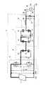
図1は、本発明の一つの実施の形態に係る太陽光発電システムの構成図であり、単相2線の場合の構成を示している。 FIG. 1 is a configuration diagram of a photovoltaic power generation system according to an embodiment of the present invention, and shows a configuration in the case of a single-phase two-wire.
この実施形態の太陽光発電システムは、太陽電池パネル1と、太陽電池パネル1からの直流電力を交流電力に変換し、商用電源2と連系運転するパワーコンディショナ3とを備えている。 The solar power generation system of this embodiment includes a solar cell panel 1 and a
太陽電池パネル1は、複数の太陽電池モジュールを直列、並列に接続して所要の発電電力を得られるように構成されている。 The solar cell panel 1 is configured to obtain a required generated power by connecting a plurality of solar cell modules in series and in parallel.
この実施形態の太陽電池パネル1は、アモルファスシリコン製の薄膜太陽電池から構成されている。 The solar cell panel 1 of this embodiment is composed of a thin film solar cell made of amorphous silicon.
この実施形態のパワーコンディショナ3は、絶縁トランスを備えていない非絶縁型(トランスレス)のパワーコンディショナである。 The
このパワーコンディショナ3は、平滑コンデンサである第1コンデンサ4と、第1〜第3チョッパ回路5〜7と、ノイズフィルタ8と、各部を制御する制御回路9とを備えており、この制御回路9は、第1〜第3チョッパ回路5〜7を制御するためのゲート信号を出力するとともに、後述のように計測回路のゲインを校正する制御部9aと、各部の電圧および出力電流を計測する計測部9bとを備えている。 The
第1〜第3チョッパ回路5〜7および制御回路9は、太陽電池パネル1に対してカスケード接続されたチョッパコンバータを構成する。 First to
太陽電池パネル1の負極側はグランドされている。図中で示す(a)点はグランドであり、このグランドの電圧はゼロである。(b)点は、太陽電池パネル1の正極側である。 The negative electrode side of the solar cell panel 1 is grounded. The point (a) shown in the figure is the ground, and the voltage of this ground is zero. The point (b) is the positive electrode side of the solar cell panel 1.
太陽電池パネル1の正負両極間に、第1コンデンサ4が並列に接続されている。 A first capacitor 4 is connected in parallel between the positive and negative electrodes of the solar cell panel 1.
第1チョッパ回路5は、第1コンデンサ4に並列に接続されている。 The
第1チョッパ回路5は、直列接続した2つの第1、第2スイッチ素子10、11を含む。第1、第2スイッチ素子10、11にはダイオードが各々逆並列に接続されている。第1チョッパ回路5は、これら2つの第1、第2スイッチ素子10、11により第1スイッチ回路を構成している。 The
第1チョッパ回路5において、第1、第2スイッチ素子10、11は、制御回路9からのゲート信号によって、系統周波数、例えば50Hzと同じ第1周波数f1で交互にON/OFF制御される。これら第1、第2スイッチ素子10、11は、第2、第3チョッパ回路6、7のスイッチ素子12〜17と同様に、例えば、NチャンネルMOSFETで構成されている。なお、スイッチ素子は、MOSFETに限らず、IGBT、トランジスタ等の他のスイッチ素子であってもよい。In the
第2チョッパ回路6は、第2コンデンサ18と、ダイオードを逆並列に接続した2つの第3、第4スイッチ素子12、13を直列接続してなる第2スイッチ回路と、を含む。第2コンデンサ18と第2スイッチ回路とは互いに並列接続されている。第3、第4スイッチ素子12、13は、制御回路9からのゲート信号によって、第1周波数f1の2倍の周波数である第2周波数f2、例えば、100Hzで交互にON/OFF制御される。The
この第2チョッパ回路6において第2コンデンサ18と第2スイッチ回路との並列接続一端側は、第1チョッパ回路5において第1、第2スイッチ素子10、11の直列接続部に接続されている。その接続点を図中(c)で示す。図中(c)(d)は第2コンデンサ18の両コンデンサ電極側に該当する。 In the
第3チョッパ回路7は、ダイオードを逆並列に接続した2つの第5、第6スイッチ素子14、15を直列接続してなる第3スイッチ回路と、第3コンデンサ19と、ダイオードを逆並列に接続した2つの第7、第8スイッチ素子16、17を直列接続してなる第4スイッチ回路とを含む。第3チョッパ回路7において、これら第3スイッチ回路、第3コンデンサ19および第4スイッチ回路は互いに並列接続されている。これら回路の並列接続一端側と他端側とをそれぞれ図中(f)(g)で示す。第3コンデンサ19の両コンデンサ電極側はこの(f)(g)に該当する。 The third chopper circuit 7 includes a third switch circuit in which two fifth and
第5、第6スイッチ素子14、15は、制御回路9からのゲート信号によって、第1周波数f1の3倍の周波数である第3周波数f3、例えば、150Hzで交互にON/OFF制御される。The fifth and
第7、第8スイッチ素子16、17は、制御回路9からのゲート信号によって、高周波数f4、例えば、18kHzでPWM制御される。 The seventh and
第3チョッパ回路7の第5、第6スイッチ素子14、15の直列接続部は、第2チョッパ回路6の第3、第4スイッチ素子12、13の直列接続部に接続されている。その接続点を図中(e)で示す。 The series connection of the fifth and
また、第3チョッパ回路7の第7、第8スイッチ素子16、17の直列接続部に、リアクトル20と第4コンデンサ21とからなるノイズフィルタ8が接続されている。その接続点を図中(h)で示す。 In addition, a
このノイズフィルタ8には、図示しない負荷および商用電源2が接続されている。 The
制御回路9は、系統電圧Vsおよび系統電流Isを、計測部9bの図示しない差動増幅回路等を介して計測し、従来と同様に商用電源2の系統周波数に同期した正弦波状の目標電圧の指令値V*を算出するとともに、第1〜第3コンデンサ4、18、19の両端の電圧Vd1、Vd2、Vd3を計測部9bの計測回路を介して計測して、各チョッパ回路5〜7を制御するためのゲート信号を生成する。The control circuit 9 measures the system voltage Vs and the system current Is via a differential amplifier circuit (not shown) of the measuring
前記電圧Vd1は、グランドである(a)点電圧を基準として(b)点に現れる太陽電池パネル1の直流出力電圧である。 The voltage Vd1 is a DC output voltage of the solar cell panel 1 that appears at point (b) with reference to the voltage at point (a) that is ground.
電圧Vd2は、第2チョッパ回路6の第2コンデンサ18の一方のコンデンサ電極点(d)を基準とした他方のコンデンサ電極点(c)での充電電圧である。 The voltage Vd2 is a charging voltage at the other capacitor electrode point (c) with the one capacitor electrode point (d) of the
電圧Vd3は、第3チョッパ回路7の第3コンデンサ19の一方のコンデンサ電極点(f)を基準とした他方のコンデンサ電極点(g)での充電電圧である。 The voltage Vd3 is a charging voltage at the other capacitor electrode point (g) with reference to one capacitor electrode point (f) of the
図2は、この実施形態の各チョッパ回路5〜7の動作の概略を説明するための図であり、同図(A)は図1の要部の構成図、同図(B)〜(D)は、同図(A)中の電圧V1、V2、V3をそれぞれ示しており、同図(B),(C)には、上述の系統に同期した正弦波状の目標電圧の指令値V*の波形を細い実線で示している。FIG. 2 is a diagram for explaining the outline of the operation of each of the
前記電圧V1は、グランドである(a)点の電位を第1基準電位とした第1チョッパ回路5の第1、第2スイッチ素子10、11の直列接続部である(c)点の電圧である。 The voltage V1 is a voltage at a point (c) which is a series connection portion of the first and
電圧V2は、前記(c)点の電位を第2基準電位とした第2チョッパ回路6の第3、第4スイッチ素子12、13の直列接続部である(e)点の電圧である。 The voltage V2 is a voltage at a point (e) which is a series connection portion of the third and
電圧V3は、第3チョッパ回路7の第5、第6のスイッチ素子14、15の直列接続部である(e)点を基準とした第7、第8のスイッチ素子16、17の直列接続部である(h)点の電圧である。 The voltage V3 is a series connection part of the seventh and
第1チョッパ回路5では、商用電源2の系統周波数と同じ50Hzの場合、系統周波数と同じ50Hzの第1周波数f1で第1、第2スイッチ素子10、11を交互にON/OFF制御する。In the
これにより、第1、第2スイッチ素子10、11の直列接続部である(c)点の電圧V1は、同図(B)に示すように、正側に立ち上がる複数の方形波電圧からなる第1方形波電圧列となる。この電圧V1の方形波の電圧レベルは、太陽電池パネル1の直流出力電圧Vd1となる。 As a result, the voltage V1 at the point (c), which is the series connection portion of the first and
第2チョッパ回路6では、第1周波数f1の2倍の周波数である100Hzの第2周波数f2で第3,第4スイッチ素子12、13を交互にON/OFF制御する。In the
これにより、第3、第4スイッチ素子12、13の直列接続部である(e)点の電圧V2は、同図(C)に示すように、第1、第2スイッチ素子10、11の直列接続部である(c)点を基準として、負側に立ち下がる複数の方形波電圧からなる第2方形波電圧列となる。 As a result, the voltage V2 at the point (e), which is the series connection portion of the third and
この電圧V2の方形波の電圧レベルは、直流出力電圧Vd1の1/2となるように制御される。 The voltage level of the square wave of the voltage V2 is controlled to be ½ of the DC output voltage Vd1.
この第2チョッパ回路6の第3、第4スイッチ素子12、13の直列接続部である(e)点の電圧V2は、グランドである(a)点を基準とした場合、すなわち、第1基準電位を基準とした場合は、後述の図4(D)に示すように、(a)−(c)点間の電圧V1と、(c)−(e)点間電圧V2とを合計した正負に交互に変化する正弦波状に対応した階段状波形の電圧V1+V2となる。この階段状の電圧V1+V2は、図4(D)に細い実線で示される上述の正弦波状の目標電圧の指令値V*と同期して正負に交互に変化する。The voltage V2 at the point (e) that is the series connection portion of the third and
第3チョッパ回路7では、この階段状波形の電圧V1+V2と、正弦波状の目標電圧の指令値V*との差電圧を補償するように第5、第6スイッチ素子14、15を、第1周波数f1の3倍の周波数である150Hzの第3周波数f3で交互にON/OFF制御し、また、第7、第8スイッチ素子16、17を、18kHzの周波数f4でPWM制御する。In the third chopper circuit 7, the fifth and
これによって、図2(A)の第3チョッパ回路7の第7、第8のスイッチ素子16、17の直列接続部である(h)点の電圧V3は、第5、第6のスイッチ素子14、15の直列接続部である(e)点を基準としてPWMの平均値で示すと、図2(D)に示すように、階段状波形の電圧V1+V2(図4(D))と、正弦波状の目標電圧の指令値V*との差電圧に対応したものとなる。As a result, the voltage V3 at the point (h), which is the series connection portion of the seventh and
したがって、第3チョッパ回路6の第7、第8スイッチ素子16、17の直列接続部である(h)点の電圧V3は、グランドである(a)点の第1基準電位を基準とした場合には、商用電源2に同期した目標電圧の指令値V*に対応した正弦波状の電圧となる。Accordingly, the voltage V3 at the point (h) that is the series connection portion of the seventh and
以下、第1〜第3チョッパ回路5〜7の動作原理を更に詳細に説明する。 Hereinafter, the operation principle of the first to
図3は、第1チョッパ回路5の動作原理を説明するための図であり、同図(A)は太陽電池パネル1、第1コンデンサ4および第1チョッパ回路5を、同図(B)は(a)−(c)間電圧V1をそれぞれ示している。特に、同図(B)には、正弦波状の目標電圧の指令値V*を細い実線で示している。FIG. 3 is a diagram for explaining the operation principle of the
太陽電池パネル1の正極側である(b)点には、グランドである(a)点の電位を第1基準電位として第1コンデンサ4で平滑化された太陽電池パネル1の直流出力電圧Vd1が現れる。 At the point (b) on the positive electrode side of the solar cell panel 1, the DC output voltage Vd1 of the solar cell panel 1 smoothed by the first capacitor 4 with the potential at the point (a) as the ground as the first reference potential is appear.
第1チョッパ回路5において、直流出力電圧Vd1は、50Hzの第1周波数f1で交互にON/OFF制御される第1、第2スイッチ素子10、11によってチョッピングされる。In the
第1スイッチ素子10がON、第2スイッチ素子11がOFFのときは、(b)点電圧である第1コンデンサ4の充電電圧Vd1が、第1チョッパ回路5の第1、第2スイッチ素子10、11の直列接続部である(c)点に現れる。 When the
第1スイッチ素子10がOFF、第2スイッチ素子11がONのときは、(a)点のグランド電圧が、第1チョッパ回路5の第1、第2スイッチ素子10、11の直列接続部である(c)点に現れる。 When the
したがって、上述のように、第1、第2スイッチ素子10、11の直列接続部である(c)点の電圧V1は、同図(B)に示すように、グランド電位を第1基準電位として正側に立ち上がる複数の方形波電圧からなる第1方形波電圧列となる。この電圧V1は、(a)点を基準とした第1、第2スイッチ素子10、11の直列接続部である(c)点の電圧であり、方形波の電圧レベルは、太陽電池パネル1の直流出力電圧Vd1、例えば、800Vとなる。 Therefore, as described above, the voltage V1 at the point (c), which is the serial connection portion of the first and
この第1チョッパ回路5では、系統の電圧と位相が一致した方形波電圧列を生成するので、有効電力を出力することができる。 Since the
図4は、第2チョッパ回路6の動作原理を説明するための図であり、同図(A)は第1チョッパ回路5および第2チョッパ回路6を、同図(B)は電圧V1を、同図(C)は電圧V2を、同図(D)は電圧V1+V2をそれぞれ示しており、同図(B)〜(D)は、正弦波状の目標電圧の指令値V*を細い実線で併せて示している。FIG. 4 is a diagram for explaining the operation principle of the
第2チョッパ回路6において、同図(B)に示される(c)点の電圧V1は、100Hzの第2周波数f2で交互にON/OFF制御される第3,第4スイッチ素子12、13により、チョッピングされる。In the
第3スイッチ素子12がON、第4スイッチ素子13がOFFのときは、第3、第4スイッチ素子12、13の直列接続部である(e)点は、第1チョッパ回路5の第1、第2スイッチ素子10、11の直列接続部である(c)点と同電位となり、第3スイッチ素子12がOFF、第4スイッチ素子13がONのときは、第3、第4スイッチ素子12、13の直列接続部である(e)点の電位は、(c)点の電位よりもマイナスとなる。したがって、第3、第4スイッチ素子12、13の直列接続部である(e)点の電圧V2は、上述のように、第1、第2スイッチ素子10、11の直列接続部である(c)点の電位を第2基準電位として同図(C)に示すように、負側に立ち下がる複数の方形波電圧からなる第2方形波電圧列となる。 When the
なお、第1チョッパ回路5の第1スイッチ素子10がON、第2スイッチ素子11がOFFしたときに、第2チョッパ回路6の第3スイッチ素子12がOFF、第4スイッチ素子13がONすることによって、第2コンデンサ18が充電される。また、第1チョッパ回路5の第1スイッチ素子10がOFF、第2スイッチ素子11がONしているときに、第2チョッパ回路6の第3スイッチ素子12がOFF、第4スイッチ素子13がONすることによって、第2コンデンサ18の充電電荷はそれらONしているスイッチ素子11,13を介して放電される。このように第2コンデンサ18は、図4(C)に示すように、充電期間T1に亘る充電と、放電期間T2に亘る放電とを交互に繰り返し、(c)点の第2基準電位を基準にして負側に立ち下がる方形波電圧が生成される。この方形波の電圧レベルVd2は、太陽電池パネル1の直流出力電圧Vd1の1/2(Vd2=−Vd1/2)、例えば、400Vである。 When the
前記電圧V2は、第1、第2スイッチ素子10、11の直列接続部である(c)点を基準とした第3、第4スイッチ素子12、13の直列接続部である(e)点の電圧である。したがって、第2チョッパ回路6では、グランドである(a)点の電位を第1基準電位として(e)点には、同図(B)の(a)−(c)点間電圧V1と、同図(C)の(c)−(e)点間電圧V2とを合計した、同図(D)に示す正弦波状の目標電圧の指令値V*の変化に対応して交互に正負に変化する階段状波形の電圧V1+V2が現れることになる。The voltage V2 is a series connection portion of the third and
この第2チョッパ回路6では、負側に立ち下がる方形波電圧列を生成するので、偶数次の高調波を除去することができ、また、等しい電力で充電と放電とを繰り返すので原理的な有効電力は、ゼロとなる。 The
また、充放電は,後述の図9(C)の系統電流Isが第2コンデンサ18を流れることで行われる。図9(C)の系統電流Isが正のとき図4(C)のT1の期間第2コンデンサ18は正弦波電流で充電される。このため、実際の動作ではT1期間徐々にV2は減少する。同様に、図9(C)の系統電流Isが負のとき図4(C)のT2の期間第2コンデンサ18は正弦波電流で放電される。このため、実際の動作ではT2期間徐々にV2は増加する。 Charging / discharging is performed when a system current Is shown in FIG. 9C described later flows through the
図5は、第3チョッパ回路7の動作原理を説明するための図であり、図6(A)は前記階段状波形の電圧V1+V2を、同図(B)は、第5、第6のスイッチ素子14、15の直列接続部である(e)点を基準として、第7、第8スイッチ素子16、17の直列接続部である(h)点の電圧V3をPWMの平均値で示したものであり、図6(A)には、正弦波状の目標電圧の指令値V*を細い実線で併せて示している。FIG. 5 is a diagram for explaining the operation principle of the third chopper circuit 7. FIG. 6A shows the voltage V1 + V2 having the stepped waveform, and FIG. 5B shows the fifth and sixth switches. The voltage V3 at the point (h) that is the series connection part of the seventh and
第5,第6スイッチ素子14、15は、図6(A)に示す(e)点の階段状波形の電圧V1+V2と正弦波状の目標電圧の指令値V*との差電圧の正負に応じたタイミングでON/OFF制御される。その結果、上記電圧V1+V2は、そのON/OFF制御のタイミングで第3コンデンサ19に充放電される。The fifth and
換言すれば、電圧V1+V2>正弦波状の目標電圧の指令値V*の関係式が成立するときは、差電圧は正であり、第5スイッチ素子14がON、第6スイッチ素子15がOFFに制御される結果、電圧V1+V2は第3コンデンサ19に充電される。In other words, when the relational expression of voltage V1 + V2> command value V* of the sine wave target voltage is established, the differential voltage is positive, and the fifth switch element 14 is controlled to be ON and the
一方、電圧V1+V2<正弦波状の目標電圧の指令値V*の関係式が成立するときは、差電圧は負であり、第5スイッチ素子14がOFF、第6スイッチ素子15がONに制御される結果、第3コンデンサ19に充電された電圧は放電される。On the other hand, when the relational expression V1 + V2 <sinusoidal target voltage command value V* is satisfied, the differential voltage is negative, and the fifth switch element 14 is controlled to be OFF and the
上記差電圧の大小関係の周期は、第3周波数f3である150Hzであり、結果として、第5,第6スイッチ素子14、15は、その第3周波数f3で交互にON/OFF制御される。Period of the magnitude relationship of the difference voltage is the third is a frequency f3 150 Hz, as a result, the fifth and
更に、第3チョッパ回路7では、電圧V1+V2と正弦波状の目標電圧の指令値V*との差電圧を補正するデューティで、第1周波数f1よりも数百倍高い周波数である18kHzの第4周波数f4で第7、第8スイッチ素子16、17をPWM制御する。これによって、第7,第8スイッチ素子16、17の直列接続部である(h)点には、図6(B)に示すように、階段状波形の電圧V1+V2と正弦波状の目標電圧の指令値V*との差電圧に対応する電圧V3が現れる。この電圧V3は、PWMの平均値を示しており、この電圧V3は、第5、第6のスイッチ素子14、15の直列接続部である(e)点を基準とした第7、第8のスイッチ素子16、17の直列接続部である(h)点の電圧である。Further, in the third chopper circuit 7, at a duty for correcting the difference voltage between the command value V* of the voltage V1 + V2 and the sine-wave target voltage, which is a several hundred times higher frequency than the
したがって、第3チョッパ回路7では、グランドである(a)点の第1基準電位を基準として、第7、第8のスイッチ素子16、17の直列接続部である(h)点には、図6(A)に示される(a)−(e)点間電圧V1+V2と、図6(B)に示される(e)−(h)点間電圧V3とを合計した、図6(A)の細い実線で示される電力系統周波数の変化と同相の正弦波状の目標電圧の指令値V*が現れることになる。Therefore, in the third chopper circuit 7, the point (h), which is the series connection portion of the seventh and
この第3チョッパ回路7では、系統周波数の3倍の周波数でチョッピングするとともに、正弦波電圧との差分をなくしているので、第3次以上の高調波を抑制することができる。 Since the third chopper circuit 7 chops at a frequency three times the system frequency and eliminates the difference from the sine wave voltage, third and higher harmonics can be suppressed.
次に、図1の制御回路9による各チョッパ回路5〜7のチョッパ制御について、更に詳細に説明する。 Next, chopper control of the
制御回路9は、第1チョッパ回路5の第1、第2スイッチ素子10、11に対するゲート信号によって、上述の図3(B)の正側に立ち上がる複数の方形波電圧のパルス幅を制御する。 The control circuit 9 controls the pulse widths of the plurality of square wave voltages that rise to the positive side in FIG. 3B described above, according to the gate signals for the first and
すなわち、第1チョッパ回路5の出力電圧の基本波成分を、系統電源の基本波電圧と一致させるように制御するものであり、方形波電圧のパルス幅δが、例えば、次式で算出される値になるように制御する。 That is, the fundamental wave component of the output voltage of the
δ=sin-1[(√2πV)/(2Vd1)]
ここで、Vは、系統電源の電圧Vsの実効値である。δ = sin−1 [(√2πV) / (2Vd1)]
Here, V is an effective value of the voltage Vs of the system power supply.
このパルス幅δを、Δδ1だけ調整すると、基本波電圧を増減することができ、このΔδ1を、計測した上述の電圧Vd3とその目標値Vd3*との誤差に係数を乗じて算出する。When the pulse width δ is adjusted by Δδ1 , the fundamental wave voltage can be increased or decreased, and Δδ1 is calculated by multiplying the error between the measured voltage Vd3 and the target value Vd3* by a coefficient.
制御回路9は、第2チョッパ回路6の第3、第4スイッチ素子12、13に対するゲート信号によって、上述の図4(C)に示される電圧Vd2が、第1チョッパ回路5の電圧Vd1の1/2になるように制御する。 The control circuit 9 uses the gate signal for the third and
すなわち、第2チョッパ回路6の第3、第4スイッチ素子12、13がゲート信号によってON/OFF制御されると、上述のように第2コンデンサ18が充電と放電とを繰り返し、図4(C)に示す負側に立ち下がる複数の方形波電圧列を生成するのであるが、充電期間T1、すなわち、充電に対応する方形波のパルス幅は、第1チョッパ回路5から出力される方形波のパルス幅と同じであり、放電期間T2、すなわち、放電に対応する方形波のパルス幅は、充電に対応する方形波のパルス幅を、Δδ2だけ微調整したものである。That is, when the third and
このΔδ2は、計測した電圧Vd2と目標とする電圧Vd2*との誤差に係数値を乗じて算出する。この目標とする電圧Vd2*を、計測した電圧Vd1の1/2の電圧としている。This Δδ2 is calculated by multiplying the error between the measured voltage Vd2 and the target voltage Vd2* by a coefficient value. This target voltage Vd2* is set to a half voltage of the measured voltage Vd1.
制御回路9は、太陽電池パネル1の発電出力の変動に応じて、方形波電圧のパルス幅を上述のように制御する。 The control circuit 9 controls the pulse width of the square wave voltage as described above according to the fluctuation of the power generation output of the solar cell panel 1.
図7および図8に、太陽電池パネル1からの入力電圧Vd1が変動した場合の正側および負側の方形波電圧V1,V2のシミュレーション波形を示す。図7は、入力電圧Vd1が800Vの場合を、図8は、入力電圧Vd1が520Vである場合をそれぞれ示している。 7 and 8 show simulation waveforms of the positive and negative square wave voltages V1, V2 when the input voltage Vd1 from the solar cell panel 1 fluctuates. FIG. 7 shows a case where the input voltage Vd1 is 800V, and FIG. 8 shows a case where the input voltage Vd1 is 520V.
図7(A)、図8(A)は正弦波状の目標電圧の指令値V*を示す。図7(B)、図8(B)は第1チョッパ回路5による正側の電圧V1を示す。図7(C)、図8(C)は第2チョッパ回路6による負側の電圧V2を示す。7A and 8A show the command value V* of the sine wave target voltage. FIGS. 7B and 8B show the positive side voltage V <b> 1 by the
入力電圧Vd1が低くなると、図8(B)に示す正側の方形波および図8(C)に示す負側の方形波のいずれのパルス幅も、図7に比べて広くなるように制御することが分かる。 When the input voltage Vd1 is lowered, the pulse widths of both the positive side square wave shown in FIG. 8B and the negative side square wave shown in FIG. 8C are controlled to be wider than those in FIG. I understand that.
また、制御回路9は、上述の図6(A)に示す階段波状の電圧V1+V2と、正弦波状の目標電圧の指令値V*との差電圧の正負に応じてタイミングで、第3チョッパ回路7の第5、第6スイッチ素子14、15を交互にON/OFF制御し、更に、前記差電圧を補正するようなデューティで、第7、第8スイッチ素子16、17を高周波数でPWM制御し、上述のように目標電圧の指令値V*の正弦波電圧を生成する。The control circuit 9 also controls the third chopper circuit 7 at the timing according to the positive or negative of the difference voltage between the stepped wave voltage V1 + V2 shown in FIG. 6A and the command value V* of the sine wave target voltage. The fifth and
図9は、図1の各部のシミュレーション波形を示すものであり、いずれもグランドを基準としている。 FIG. 9 shows a simulation waveform of each part of FIG. 1, and all are based on the ground.
図9(A)は系統電圧Vs、図9(B)は第3チョッパ回路7の出力電圧V、図9(C)は系統電流Is、図9(D)は電圧V1およびV2(破線)、図9(E)は電圧V3、図9(F)は電圧Vd2およびVd3(破線)である。 9A shows the system voltage Vs, FIG. 9B shows the output voltage V of the third chopper circuit 7, FIG. 9C shows the system current Is, FIG. 9D shows the voltages V1 and V2 (broken lines), FIG. 9E shows the voltage V3, and FIG. 9F shows the voltages Vd2 and Vd3 (broken lines).
この実施形態では、上述のように、第1チョッパ回路5の第1、第2スイッチ素子10、11は、例えば、800Vの電圧を50Hzの第1周波数f1でスイッチングし、第2チョッパ回路6の第3、第4スイッチ素子12、13は、例えば、400Vの電圧を100Hzの第2周波数f2でスイッチングし、第3チョッパ回路7の第5、第6スイッチ素子14、15は、例えば、260Vの電圧を150Hzの第3周波数f3でスイッチングしている。すなわち、これらスイッチ素子10〜15は、従来のパワーコンディショナのPWM制御のインバータのPWM周波数に比べて、はるかに低い周波数でスイッチングしている。In this embodiment, as described above, the first and
また、第3チョッパ回路7の第7、第8スイッチ素子16、17は、階段波状の電圧V1+V2と、正弦波状の目標電圧の指令値V*との差電圧である260V程度の電圧を18kHzの高い周波数でPWM制御している。すなわち、第7、第8スイッチ素子16、17では、従来のパワーコンディショナのPWM制御のインバータに比べて、低い電圧をスイッチングしている。The seventh and
このように、第1〜第3チョッパ回路5〜7の第1〜6スイッチ素子10〜15では、従来のPWM制御に比べて、はるかに低い周波数でスイッチングしているので、スイッチング損失を低減できるとともに、導通損失の低いスイッチ素子や安価なスイッチ素子を選択することができる一方、第3チョッパ回路7の第7、第8スイッチ素子16、17では、従来のPWM制御に比べて低い電圧をスイッチングするので、スイッチング損失を低減することが可能となる。 As described above, since the first to
これによって、パワーコンディショナ3の電力変換効率を、従来例のパワーコンディショナに比べて向上させることができる。 Thereby, the power conversion efficiency of the
なお、方形波電圧生成手段は、第1チョッパ回路5、第2チョッパ回路6、第3チョッパ回路7の第5、第6スイッチ素子14、15および第3コンデンサ19、並びに、それらを制御する制御回路9を含み、正弦波電圧生成手段は、第3チョッパ回路7の第7、第8スイッチ素子16、17およびそれらを制御する制御回路9を含む。 The square wave voltage generating means includes the
この実施形態では、太陽電池パネル1は、上述のようにアモルファスシリコン製の薄膜太陽電池から構成されている。 In this embodiment, the solar cell panel 1 is composed of a thin-film solar cell made of amorphous silicon as described above.
かかるアモルファスシリコン製の太陽電池では、その負極側電位がグランド電位より低くなると、経年劣化を起こすことが知られており、その対策のため、その負極側をグランド電位にする必要がある。 In such an amorphous silicon solar cell, it is known that when the negative electrode side potential becomes lower than the ground potential, the aging deterioration occurs, and the negative electrode side needs to be set to the ground potential as a countermeasure.
しかしながら、上述の図18に示される非絶縁型のパワーコンディショナ36では、直流側と交流側とでは、基準電位のレベルが異なるために、パワーコンディショナ36の入力側である太陽電池の負極側をグランド電位にすることができない。これに対して、本発明では、直流側と交流側との基準電位のレベルが同じであるので、太陽電池の負極側をグランド電位にすることが可能となる。 However, in the
上述の実施形態では、単相2線の場合に適用して説明したけれども、本発明の他の実施形態として、図10に示すように単相3線、図11に示すように三相3線、あるいは、図12に示すように三相4線に適用してもよい。 In the above-described embodiment, the description is applied to the case of single-phase two-wire. However, as another embodiment of the present invention, single-phase three-wire as shown in FIG. 10, three-phase three-wire as shown in FIG. Alternatively, it may be applied to a three-phase four-wire as shown in FIG.
図13は、図15に示す三相4線の場合の本実施形態と、図14に示される従来方式との特性を比較して示すものであり、横軸は出力電力(W)を、縦軸は効率(%)を示している。同図において、実線は、本実施形態の特性を示し、太い実線はSJ(スーパージャンクション)MOSFETを、細い実線はIGBTを、スイッチ素子としてそれぞれ使用した場合の特性を示しており、破線は、従来方式の特性を示している。 FIG. 13 shows a comparison of the characteristics of the present embodiment in the case of the three-phase four-wire shown in FIG. 15 and the conventional method shown in FIG. The axis indicates efficiency (%). In the figure, the solid line shows the characteristics of this embodiment, the thick solid line shows the characteristics when using an SJ (Super Junction) MOSFET, the thin solid line shows the characteristics when using the IGBT as a switching element, and the broken line shows the conventional characteristics. The characteristics of the method are shown.
なお、この図13は、系統線間電圧400V、入力電圧570Vの場合を示している。また、従来方式は、図14に示すように、リアクトル28、ダイオード29、IGBT30およびスイッチ31を含む昇圧回路32、平滑コンデンサ41およびPWM制御のインバータ42を備える非絶縁型のパワーコンディショナである。 FIG. 13 shows a case where the system line voltage is 400V and the input voltage is 570V. As shown in FIG. 14, the conventional system is a non-insulated power conditioner including a
この図13に示すように、本実施形態では、従来方式に比べて、効率が向上していることが分かる。 As shown in FIG. 13, it can be seen that the efficiency is improved in the present embodiment as compared with the conventional method.
更に、この実施形態では、出力電圧にスパイク状のノイズ等が生じないように次のようにしている。 Furthermore, in this embodiment, the following is performed so that spike noise or the like does not occur in the output voltage.
正弦波状の目標電圧の指令値V*は、上述のように、計測した電圧Vd1、Vd2、Vd3を参照して算出されるものである。The sine wave target voltage command value V* is calculated with reference to the measured voltages Vd1, Vd2, and Vd3 as described above.
ここで、電圧Vd1、Vd2、Vd3は、制御回路9の計測部9bにおいて、対応する各計測回路を用いて計測するのであるが、各計測回路を構成する部品のバラツキなどに起因して、同じ電圧であるにも拘らず、計測値が異なる場合があり、特に、温度の低い場所や高い場所では、計測値の相違が大きくなる。 Here, the voltages Vd1, Vd2, and Vd3 are measured using the corresponding measurement circuits in the
このように電圧Vd1、Vd2、Vd3をそれぞれ計測する各計測回路に誤差が生じると、上述のように正弦波状の目標電圧の指令値V*に誤差が生じ、スイッチ素子のON/OFFの切換えの瞬間に、誤差の分だけずれた電圧を生成してスパイク状のノイズが生じることになる。As described above, when an error occurs in each measurement circuit that measures the voltages Vd1, Vd2, and Vd3, an error occurs in the command value V* of the sine wave target voltage as described above, and switching of the switch element ON / OFF is performed. At a moment, a voltage shifted by an error is generated, and spike-like noise is generated.
このため、この実施形態では、同じ計測電圧に対して、各計測回路の計測値が一致するように、各計測回路のゲインを自動校正するようにしている。 For this reason, in this embodiment, the gain of each measurement circuit is automatically calibrated so that the measurement value of each measurement circuit matches the same measurement voltage.
この実施形態では、電圧Vd1の計測回路を基準として、電圧Vd2、Vd3の計測回路のゲインを校正するようにしている。 In this embodiment, the gains of the measurement circuits for the voltages Vd2 and Vd3 are calibrated using the measurement circuit for the voltage Vd1 as a reference.
図16は、電圧Vd1の計測回路を基準として、電圧Vd2の計測回路を校正する場合の構成図であり、上述の図1に対応する部分には、同一の参照符号を付す。 FIG. 16 is a configuration diagram in the case where the measurement circuit for the voltage Vd2 is calibrated with reference to the measurement circuit for the voltage Vd1, and parts corresponding to those in FIG. 1 are given the same reference numerals.
この実施形態では、運転の開始前に、図示しない連系リレーを開いて系統と切り離した状態で、出力短絡リレー50を閉じて、第1コンデンサ4の両端の電圧Vd1と第2コンデンサ18の両端の電圧Vd2とが同じ電圧になるように各スイッチ素子10〜17のON/OFFを制御する。 In this embodiment, before starting the operation, in a state where the interconnection relay (not shown) is opened and disconnected from the system, the output short-
具体的には、第1スイッチ素子10、第4スイッチ素子13、第6スイッチ素子15および第8スイッチ素子17をONする一方、第2スイッチ素子11、第3スイッチ素子12、第5スイッチ素子14および第7スイッチ素子16をOFFし、第1コンデンサ4の両端の電圧Vd1と第2コンデンサ18の両端の電圧Vd2とが同じ電圧となるようにスイッチング制御し、各電圧Vd1、Vd2を計測する。 Specifically, the
これによって、電圧Vd2の計測回路の計測値が、電圧Vd1の計測回路の計測値に一致するように補正するための補正係数が次式によって算出される。 Accordingly, a correction coefficient for correcting the measurement value of the measurement circuit of the voltage Vd2 so as to coincide with the measurement value of the measurement circuit of the voltage Vd1 is calculated by the following equation.
補正係数=電圧Vd1の計測値÷電圧Vd2の計測値
この補正係数が求められた後の通常の運転時には、計測回路で計測される電圧Vd2の計測値(補正前計測値)に、前記係数を乗じることによって、電圧Vd2の計測値を補正した補正後の計測値を得ることができる。Correction coefficient = Measured value of voltage Vd1 / Measured value of voltage Vd2 During normal operation after the correction coefficient is obtained, the coefficient is added to the measured value (measured value before correction) of voltage Vd2 measured by the measurement circuit. By multiplying, it is possible to obtain a corrected measurement value obtained by correcting the measurement value of the voltage Vd2.
すなわち、電圧Vd2の補正後の計測値は、次式で算出される。 That is, the measured value after the correction of the voltage Vd2 is calculated by the following equation.
電圧Vd2の補正後の計測値=補正係数×電圧Vd2の補正前の計測値
このようにして同一の電圧に対する電圧Vd1の計測回路と電圧Vd2の計測回路の計測値を一致させることができる。Measurement value after correction of voltage Vd2 = correction coefficient × measurement value before correction of voltage Vd2 In this way, the measurement values of the measurement circuit of voltage Vd1 and the measurement circuit of voltage Vd2 for the same voltage can be matched.
図17は、電圧Vd1の計測回路を基準として、電圧Vd3の計測回路を校正する場合の構成図であり、上述の図1に対応する部分には、同一の参照符号を付す。 FIG. 17 is a configuration diagram in the case where the measurement circuit for the voltage Vd3 is calibrated with reference to the measurement circuit for the voltage Vd1, and parts corresponding to those in FIG. 1 are given the same reference numerals.
電圧Vd2の計測回路の校正の場合と同様に、連系リレーを開いて系統と切り離した状態で、出力短絡リレー50を閉じて、第1コンデンサ4の両端の電圧Vd1と第3コンデンサ19の両端の電圧Vd3とが同じ電圧になるように各スイッチ素子10〜17のON/OFFを制御する。 Similarly to the calibration of the measurement circuit for the voltage Vd2, the output short-
具体的には、第1スイッチ素子10、第3スイッチ素子12、第5スイッチ素子14および第8スイッチ素子17をONする一方、第2スイッチ素子11、第4スイッチ素子13、第6スイッチ素子15および第7スイッチ素子16をOFFし、第1コンデンサ4の両端の電圧Vd1と第3コンデンサ19の両端の電圧Vd3とが同じ電圧となるようにスイッチング制御し、各電圧Vd1、Vd3をそれぞれ計測する。 Specifically, the
これによって、電圧Vd3の計測回路の計測値が、電圧Vd1の計測回路の計測値に一致するように補正するための補正係数が次式によって算出される。 Accordingly, a correction coefficient for correcting the measurement value of the measurement circuit of the voltage Vd3 so as to coincide with the measurement value of the measurement circuit of the voltage Vd1 is calculated by the following equation.
補正係数=電圧Vd1の計測値÷電圧Vd3の計測値
この補正係数が求められた後の通常の運転時には、計測回路で計測される電圧Vd3の計測値(補正前計測値)に、前記係数を乗じることによって、電圧Vd3の計測値を補正した補正後の計測値を得ることができる。Correction coefficient = Measurement value of voltage Vd1 ÷ Measurement value of voltage Vd3 During normal operation after the correction coefficient is obtained, the coefficient is added to the measurement value (measurement value before correction) of voltage Vd3 measured by the measurement circuit. By multiplying, it is possible to obtain a corrected measurement value obtained by correcting the measurement value of the voltage Vd3.
すなわち、電圧Vd3の補正後の計測値は、次式で算出される。 That is, the measured value after the correction of the voltage Vd3 is calculated by the following equation.
電圧Vd3の補正後の計測値=補正係数×電圧Vd3の補正前の計測値
このようにして同一の電圧に対する電圧Vd1の計測回路と電圧Vd3の計測回路の計測値を一致させることができる。Measurement value after correction of voltage Vd3 = correction coefficient × measurement value before correction of voltage Vd3 In this way, the measurement values of the measurement circuit of voltage Vd1 and the measurement circuit of voltage Vd3 with respect to the same voltage can be matched.
以上のようにして、同一の電圧に対する電圧Vd1、Vd2、Vd3の各計測回路の計測値を一致させることができ、これによって、計測値の誤差に起因する交流電圧のスパイクノイズを抑制することができる。 As described above, the measurement values of the measurement circuits of the voltages Vd1, Vd2, and Vd3 with respect to the same voltage can be matched, thereby suppressing the spike noise of the AC voltage caused by the measurement value error. it can.
本発明は、電力変換装置として有用である。 The present invention is useful as a power converter.
1 太陽電池パネル
2 商用電源
3 パワーコンディショナ
5 第1チョッパ回路
6 第2チョッパ回路
7 第3チョッパ回路
9 制御回路
10〜17 第1〜第8スイッチ素子DESCRIPTION OF SYMBOLS 1
Claims (4)
Translated fromJapanese前記第1方形波電圧列の電位を第2基準電位とし、前記第1手段の出力を前記第1周波数より高い第2周波数でチョッピングして電圧レベルが前記正側の第1方形波電圧列より低電圧で前記第2基準電位に対して負側に変化する複数の方形波電圧からなる第2方形波電圧列を生成すると共に、前記第1、第2方形波電圧列を加算することでそれらが前記第1基準電位に対してその正負両側に交互に正弦波的に変化する第3方形波電圧列を形成する第2手段と、
前記第3方形波電圧列を正弦波電圧との差分の正負に応じたタイミングで定まる第3周波数でチョッピングして充放電出力する第3手段と、
前記第3手段の充放電出力を、前記第3方形波電圧列と前記正弦波電圧との差分を補正するように、前記第3周波数よりも高いPWM周波数でPWM制御すると共に、前記第3方形波電圧列と前記PWM出力とで前記第1基準電位に対して正負両側に連続して変化する正弦波電圧を得る第4手段とを具備し、
前記第1手段は、2つの第1、第2スイッチ素子を直列接続してなる第1スイッチ回路を含み、前記第1スイッチ回路は、直流電力源の正負両極間に接続された第1コンデンサに並列接続され、
前記第2手段は、第2コンデンサと第2スイッチ回路との並列接続回路を含み、前記並列接続回路の並列接続一方側が、前記第1、第2スイッチ素子の直列接続部に接続され、前記第2スイッチ回路は、2つの第3、第4スイッチ素子を直列接続してなり、
前記第3手段は、第3スイッチ回路と第3コンデンサとの並列接続回路を含み、前記第3スイッチ回路は、2つの第5、第6スイッチ素子を直列接続してなり、前記第5、第6スイッチ素子の直列接続部が、前記第3、第4スイッチ素子の直列接続部に接続され、
前記第4手段は、第3手段の前記並列接続回路に並列に接続された第4スイッチ回路を含み、前記第4スイッチ回路は、2つの第7、第8スイッチ素子を直列接続してなり、
前記第1コンデンサ、前記第2コンデンサ、および、前記第3コンデンサの各両端電圧をそれぞれ計測する各計測回路と、
前記各計測回路の計測値に基づいて、前記第1〜第8の各スイッチ素子を制御する制御手段と、
前記各計測回路のゲインを校正するゲイン校正手段と、
を具備したことを特徴とする電力変換装置。First means for chopping a DC voltage at a first frequency to generate a first square-wave voltage string composed of a plurality of square-wave voltages whose voltage level changes to the positive side with respect to the first reference potential;
The potential of the first square wave voltage string is set as a second reference potential, and the output of the first means is chopped at a second frequency higher than the first frequency, so that the voltage level is higher than the first square wave voltage string having the positive side. Generating a second square wave voltage string composed of a plurality of square wave voltages that change to the negative side with respect to the second reference potential at a low voltage, and adding the first and second square wave voltage strings to add them A second means for forming a third square wave voltage train that alternately changes sinusoidally on both positive and negative sides with respect to the first reference potential;
Third means for chopping the third square wave voltage train at a third frequency determined at a timing corresponding to the sign of the difference from the sine wave voltage, and charging and discharging,
The charge / discharge output of the third means is PWM controlled at a PWM frequency higher than the third frequency so as to correct the difference between the third square wave voltage train and the sine wave voltage, and the third square shape A fourth means for obtaining a sinusoidal voltage that continuously changes on both positive and negative sides with respect to the first reference potential by a wave voltage train and the PWM output;
The first means includes a first switch circuit formed by connecting two first and second switch elements in series, and the first switch circuit is connected to a first capacitor connected between the positive and negative electrodes of a DC power source. Connected in parallel,
The second means includes a parallel connection circuit of a second capacitor and a second switch circuit, wherein one side of the parallel connection circuit connected in parallel is connected to a series connection portion of the first and second switch elements, and A two-switch circuit is formed by connecting two third and fourth switch elements in series,
The third means includes a parallel connection circuit of a third switch circuit and a third capacitor, and the third switch circuit is formed by connecting two fifth and sixth switch elements in series, and the fifth, sixth, A serial connection of 6 switch elements is connected to the serial connection of the third and fourth switch elements;
The fourth means includes a fourth switch circuit connected in parallel to the parallel connection circuit of the third means, and the fourth switch circuit is formed by connecting two seventh and eighth switch elements in series,
Each measurement circuit for measuring the voltage across each of the first capacitor, the second capacitor, and the third capacitor,
Control means for controlling the first to eighth switch elements based on the measurement values of the measurement circuits;
Gain calibration means for calibrating the gain of each measurement circuit;
A power conversion device comprising:
前記ゲイン校正手段は、前記同一の電圧が印加された二つのコンデンサにそれぞれ対応する二つの計測回路の計測値に基づいて、ゲインを校正する請求項1に記載の電力変換装置。The control means short-circuits the output of the fourth means so that the same voltage is applied across both of the first capacitor, the second capacitor, and the third capacitor, and the first capacitor 1 to 8 switch elements are controlled,
The power conversion device according to claim 1, wherein the gain calibration means calibrates the gain based on measurement values of two measurement circuits respectively corresponding to the two capacitors to which the same voltage is applied.
前記ゲイン校正手段は、前記同一の電圧が印加される前記基準のコンデンサに対応する計測回路の計測値を基準として他の二つの計測回路のゲインを校正する請求項2に記載の電力変換装置。The control means uses one of the first capacitor, the second capacitor, and the third capacitor as a reference, and the same voltage is applied to both ends of each of the two capacitors including the reference capacitor. Control and
The power conversion device according to claim 2, wherein the gain calibration unit calibrates gains of the other two measurement circuits based on a measurement value of the measurement circuit corresponding to the reference capacitor to which the same voltage is applied.
前記直流電力源からの直流電圧を、系統周波数である第1周波数でチョッピングして電圧レベルが第1基準電位に対して正側に変化する複数の方形波電圧からなる第1方形波電圧列を、生成する第1手段と、
前記第1方形波電圧列の電位を第2基準電位とし、前記第1手段の出力を前記第1周波数より所定倍高い第2周波数でチョッピングして電圧レベルが前記正側の第1方形波電圧列より低電圧で前記第2基準電位に対して負側に変化する複数の方形波電圧からなる第2方形波電圧列を生成すると共に、前記第1、第2方形波電圧列を加算することでそれらが前記第1基準電位に対してその正負両側に交互に正弦波的に変化する第3方形波電圧列を形成する第2手段と、
前記第3方形波電圧列を正弦波電圧との差分の正負に応じたタイミングで定まる第3周波数でチョッピングして充放電出力させる第3手段と、
前記第3手段の充放電出力を、前記第3方形波電圧列と前記正弦波電圧との差分を補正するように、前記第3周波数よりも高いPWM周波数でPWM制御すると共に、前記第3方形波電圧列と前記PWM出力とで前記第1基準電位に対して正負両側に連続して変化する正弦波電圧を得ると共に、この正弦波電圧を負荷側に出力する第4手段とを具備し、
前記第1手段は、2つの第1、第2スイッチ素子を直列接続してなる第1スイッチ回路を含み、前記第1スイッチ回路は、直流電力源の正負両極間に接続された第1コンデンサに並列接続され、
前記第2手段は、第2コンデンサと第2スイッチ回路との並列接続回路を含み、前記並列接続回路の並列接続一方側が、前記第1、第2スイッチ素子の直列接続部に接続され、前記第2スイッチ回路は、2つの第3、第4スイッチ素子を直列接続してなり、
前記第3手段は、第3スイッチ回路と第3コンデンサとの並列接続回路を含み、前記第3スイッチ回路は、2つの第5、第6スイッチ素子を直列接続してなり、前記第5、第6スイッチ素子の直列接続部が、前記第3、第4スイッチ素子の直列接続部に接続され、
前記第4手段は、第3手段の前記並列接続回路に並列に接続された第4スイッチ回路を含み、前記第4スイッチ回路は、2つの第7、第8スイッチ素子を直列接続してなり、
前記第1コンデンサ、前記第2コンデンサ、および、前記第3コンデンサの各両端電圧をそれぞれ計測する各計測回路と、
前記各計測回路の計測値に基づいて、前記第1〜第8の各スイッチ素子を制御する制御手段と、
前記各計測回路のゲインを校正するゲイン校正手段と、
を具備したことを特徴とするパワーコンディショナ。In a power conditioner that converts DC power from a DC power source into AC power grid-connected to a commercial power source,
A DC voltage from the DC power source is chopped at a first frequency, which is a system frequency, and a first square wave voltage string including a plurality of square wave voltages whose voltage level changes to the positive side with respect to the first reference potential is obtained. First means for generating;
The potential of the first square wave voltage train is set as a second reference potential, and the output of the first means is chopped at a second frequency that is a predetermined multiple higher than the first frequency, and the voltage level is the first square wave voltage on the positive side. Generating a second square-wave voltage sequence composed of a plurality of square-wave voltages that are lower than the sequence and change negatively with respect to the second reference potential, and adding the first and second square-wave voltage sequences And a second means for forming a third square wave voltage train that alternately changes sinusoidally on both positive and negative sides with respect to the first reference potential;
A third means for chopping the third square wave voltage train at a third frequency determined at a timing corresponding to the positive or negative of the difference from the sine wave voltage, and charging and discharging;
The charge / discharge output of the third means is PWM controlled at a PWM frequency higher than the third frequency so as to correct the difference between the third square wave voltage train and the sine wave voltage, and the third square shape A sine wave voltage continuously changing on both positive and negative sides with respect to the first reference potential by a wave voltage train and the PWM output, and a fourth means for outputting the sine wave voltage to the load side,
The first means includes a first switch circuit formed by connecting two first and second switch elements in series, and the first switch circuit is connected to a first capacitor connected between the positive and negative electrodes of a DC power source. Connected in parallel,
The second means includes a parallel connection circuit of a second capacitor and a second switch circuit, wherein one side of the parallel connection circuit connected in parallel is connected to a series connection portion of the first and second switch elements, and A two-switch circuit is formed by connecting two third and fourth switch elements in series,
The third means includes a parallel connection circuit of a third switch circuit and a third capacitor, and the third switch circuit is formed by connecting two fifth and sixth switch elements in series, and the fifth, sixth, A serial connection of 6 switch elements is connected to the serial connection of the third and fourth switch elements;
The fourth means includes a fourth switch circuit connected in parallel to the parallel connection circuit of the third means, and the fourth switch circuit is formed by connecting two seventh and eighth switch elements in series,
Each measurement circuit for measuring the voltage across each of the first capacitor, the second capacitor, and the third capacitor,
Control means for controlling the first to eighth switch elements based on the measurement values of the measurement circuits;
Gain calibration means for calibrating the gain of each measurement circuit;
A power conditioner comprising:
Priority Applications (5)
| Application Number | Priority Date | Filing Date | Title |
|---|---|---|---|
| JP2010052761AJP5071498B2 (en) | 2010-03-10 | 2010-03-10 | Power converter and power conditioner |
| KR1020110000824AKR101186364B1 (en) | 2010-03-10 | 2011-01-05 | Power conversion apparatus and power conditioner |
| EP11151243.0AEP2365626B1 (en) | 2010-03-10 | 2011-01-18 | Power converter and power conditioner |
| US13/034,056US8462526B2 (en) | 2010-03-10 | 2011-02-24 | DC/AC chopper type power converter for non-insulated type power conditioner with gain calibration of measuring circuit |
| CN201110046134.3ACN102195500B (en) | 2010-03-10 | 2011-02-25 | Power converter and power conditioner |
Applications Claiming Priority (1)
| Application Number | Priority Date | Filing Date | Title |
|---|---|---|---|
| JP2010052761AJP5071498B2 (en) | 2010-03-10 | 2010-03-10 | Power converter and power conditioner |
Publications (2)
| Publication Number | Publication Date |
|---|---|
| JP2011188663A JP2011188663A (en) | 2011-09-22 |
| JP5071498B2true JP5071498B2 (en) | 2012-11-14 |
Family
ID=44262898
Family Applications (1)
| Application Number | Title | Priority Date | Filing Date |
|---|---|---|---|
| JP2010052761AActiveJP5071498B2 (en) | 2010-03-10 | 2010-03-10 | Power converter and power conditioner |
Country Status (5)
| Country | Link |
|---|---|
| US (1) | US8462526B2 (en) |
| EP (1) | EP2365626B1 (en) |
| JP (1) | JP5071498B2 (en) |
| KR (1) | KR101186364B1 (en) |
| CN (1) | CN102195500B (en) |
Families Citing this family (12)
| Publication number | Priority date | Publication date | Assignee | Title |
|---|---|---|---|---|
| JP5477237B2 (en)* | 2010-09-13 | 2014-04-23 | オムロン株式会社 | Inverter |
| TWI481146B (en)* | 2011-12-02 | 2015-04-11 | Darfon Electronics Corp | Off-grid solar inverter system without a battery and control method thereof |
| CN102938575B (en)* | 2012-11-21 | 2014-09-17 | 无锡北方湖光光电有限公司 | Portable universal power supply support system for field operations |
| JP6119332B2 (en)* | 2013-03-15 | 2017-04-26 | オムロン株式会社 | Inverter and program |
| WO2017010142A1 (en)* | 2015-07-14 | 2017-01-19 | 三菱電機株式会社 | Power conversion device |
| US10141851B2 (en)* | 2016-03-25 | 2018-11-27 | General Electric Company | Resonant DC to DC power converter |
| CN109565245B (en)* | 2016-08-12 | 2021-07-09 | 马里奇控股荷兰有限公司 | Recovery of deteriorated photovoltaic panels |
| JP2018152996A (en)* | 2017-03-13 | 2018-09-27 | オムロン株式会社 | Distributed power supply |
| EP3610567B1 (en)* | 2017-04-10 | 2025-06-04 | Berner Fachhochschule | Efficient electric power conversion |
| US11005388B2 (en)* | 2019-02-28 | 2021-05-11 | sonnen, Inc. | Single-phase multi-level asymmetric inverter with AC-bypass and asymmetric modulation strategy |
| US20220393599A1 (en)* | 2019-11-08 | 2022-12-08 | Rensselaer Polytechnic Institute | High-voltage power supply system |
| JPWO2024105841A1 (en)* | 2022-11-17 | 2024-05-23 |
Family Cites Families (21)
| Publication number | Priority date | Publication date | Assignee | Title |
|---|---|---|---|---|
| US4674024A (en)* | 1986-06-05 | 1987-06-16 | Westinghouse Electric Corp. | High voltage modular inverter and control system thereof |
| DE19720787A1 (en)* | 1997-05-17 | 1998-11-19 | Asea Brown Boveri | Method for operating a power electronic circuit arrangement |
| JP3418906B2 (en)* | 1997-12-24 | 2003-06-23 | オムロン株式会社 | DC / DC converter and power conditioner |
| JP2000116005A (en)* | 1998-10-02 | 2000-04-21 | Sanken Electric Co Ltd | Ac power unit |
| JP3941346B2 (en) | 2000-06-16 | 2007-07-04 | オムロン株式会社 | Power conditioner in solar power generation system |
| JP2002252986A (en)* | 2001-02-26 | 2002-09-06 | Canon Inc | Inverter, power supply system and method of reducing leakage current in power supply system |
| US6556461B1 (en)* | 2001-11-19 | 2003-04-29 | Power Paragon, Inc. | Step switched PWM sine generator |
| FR2858725B1 (en)* | 2003-08-06 | 2005-10-07 | St Microelectronics Sa | SELF-PORTABLE DEVICE FOR GENERATING A HIGH VOLTAGE, AND METHOD FOR REPAIRING A DEVICE FOR GENERATING A HIGH VOLTAGE. |
| US7596008B2 (en)* | 2005-02-25 | 2009-09-29 | Mitsubishi Electric Corporation | Power conversion apparatus |
| TW200709544A (en)* | 2005-08-29 | 2007-03-01 | Ind Tech Res Inst | Transformer-free power conversion circuit for parallel connection with commercial electricity system |
| JP2007166874A (en)* | 2005-12-16 | 2007-06-28 | Toyota Motor Corp | Voltage converter |
| JP4755504B2 (en)* | 2006-02-16 | 2011-08-24 | 三菱電機株式会社 | Power converter |
| US7692938B2 (en)* | 2006-09-06 | 2010-04-06 | Northern Power Systems, Inc. | Multiphase power converters and multiphase power converting methods |
| US7974106B2 (en)* | 2007-05-07 | 2011-07-05 | Bloom Energy Corporation | Ripple cancellation |
| JP4968465B2 (en)* | 2007-07-18 | 2012-07-04 | 三菱電機株式会社 | Power converter |
| KR101183507B1 (en)* | 2008-06-09 | 2012-09-20 | 에이비비 테크놀로지 아게 | A voltage source converter |
| US20100141230A1 (en)* | 2008-07-17 | 2010-06-10 | Exar Corporation | Self-tuning sensorless digital current-mode controller with accurate current sharing for multiphase dc-dc converters |
| KR100975925B1 (en)* | 2008-07-25 | 2010-08-13 | 삼성전기주식회사 | Adapter power supply |
| EP2391521B1 (en)* | 2009-01-29 | 2020-03-25 | Brusa Elektronik AG | Converter for single-phase and three-phase operation, d.c. voltage supply and battery charger |
| JP4911733B2 (en)* | 2009-03-13 | 2012-04-04 | オムロン株式会社 | Power converter, power conditioner, and power generation system |
| JP4888817B2 (en)* | 2009-03-13 | 2012-02-29 | オムロン株式会社 | Power conditioner and photovoltaic system |
- 2010
- 2010-03-10JPJP2010052761Apatent/JP5071498B2/enactiveActive
- 2011
- 2011-01-05KRKR1020110000824Apatent/KR101186364B1/enactiveActive
- 2011-01-18EPEP11151243.0Apatent/EP2365626B1/ennot_activeNot-in-force
- 2011-02-24USUS13/034,056patent/US8462526B2/enactiveActive
- 2011-02-25CNCN201110046134.3Apatent/CN102195500B/ennot_activeExpired - Fee Related
Also Published As
| Publication number | Publication date |
|---|---|
| KR20110102143A (en) | 2011-09-16 |
| JP2011188663A (en) | 2011-09-22 |
| CN102195500A (en) | 2011-09-21 |
| EP2365626A3 (en) | 2014-05-28 |
| KR101186364B1 (en) | 2012-09-26 |
| US20110235384A1 (en) | 2011-09-29 |
| EP2365626A2 (en) | 2011-09-14 |
| US8462526B2 (en) | 2013-06-11 |
| CN102195500B (en) | 2014-01-22 |
| EP2365626B1 (en) | 2017-03-15 |
Similar Documents
| Publication | Publication Date | Title |
|---|---|---|
| JP5071498B2 (en) | Power converter and power conditioner | |
| JP4911733B2 (en) | Power converter, power conditioner, and power generation system | |
| JP4888817B2 (en) | Power conditioner and photovoltaic system | |
| US20180026547A1 (en) | Maximizing power in a photovoltaic distributed power system | |
| JP5045772B2 (en) | Capacitor capacity missing detection method in power conditioner, power conditioner for implementing the same, and photovoltaic power generation system including the same | |
| Beser et al. | A grid-connected photovoltaic power conversion system with single-phase multilevel inverter | |
| JP5477237B2 (en) | Inverter | |
| JP2024023924A (en) | power system | |
| JP5375781B2 (en) | Inverter | |
| JP5163673B2 (en) | Control circuit, power conditioner including the control circuit, and photovoltaic power generation system |
Legal Events
| Date | Code | Title | Description |
|---|---|---|---|
| A621 | Written request for application examination | Free format text:JAPANESE INTERMEDIATE CODE: A621 Effective date:20120301 | |
| A977 | Report on retrieval | Free format text:JAPANESE INTERMEDIATE CODE: A971007 Effective date:20120702 | |
| TRDD | Decision of grant or rejection written | ||
| A01 | Written decision to grant a patent or to grant a registration (utility model) | Free format text:JAPANESE INTERMEDIATE CODE: A01 Effective date:20120724 | |
| A01 | Written decision to grant a patent or to grant a registration (utility model) | Free format text:JAPANESE INTERMEDIATE CODE: A01 | |
| A61 | First payment of annual fees (during grant procedure) | Free format text:JAPANESE INTERMEDIATE CODE: A61 Effective date:20120806 | |
| R150 | Certificate of patent or registration of utility model | Ref document number:5071498 Country of ref document:JP Free format text:JAPANESE INTERMEDIATE CODE: R150 Free format text:JAPANESE INTERMEDIATE CODE: R150 | |
| FPAY | Renewal fee payment (event date is renewal date of database) | Free format text:PAYMENT UNTIL: 20150831 Year of fee payment:3 |