JP5069735B2 - Driver circuit for voltage-driven switching device - Google Patents
Driver circuit for voltage-driven switching deviceDownload PDFInfo
- Publication number
- JP5069735B2 JP5069735B2JP2009242497AJP2009242497AJP5069735B2JP 5069735 B2JP5069735 B2JP 5069735B2JP 2009242497 AJP2009242497 AJP 2009242497AJP 2009242497 AJP2009242497 AJP 2009242497AJP 5069735 B2JP5069735 B2JP 5069735B2
- Authority
- JP
- Japan
- Prior art keywords
- voltage
- gate
- switching device
- current
- transistor
- Prior art date
- Legal status (The legal status is an assumption and is not a legal conclusion. Google has not performed a legal analysis and makes no representation as to the accuracy of the status listed.)
- Expired - Fee Related
Links
Images


Classifications
- Y—GENERAL TAGGING OF NEW TECHNOLOGICAL DEVELOPMENTS; GENERAL TAGGING OF CROSS-SECTIONAL TECHNOLOGIES SPANNING OVER SEVERAL SECTIONS OF THE IPC; TECHNICAL SUBJECTS COVERED BY FORMER USPC CROSS-REFERENCE ART COLLECTIONS [XRACs] AND DIGESTS
- Y02—TECHNOLOGIES OR APPLICATIONS FOR MITIGATION OR ADAPTATION AGAINST CLIMATE CHANGE
- Y02B—CLIMATE CHANGE MITIGATION TECHNOLOGIES RELATED TO BUILDINGS, e.g. HOUSING, HOUSE APPLIANCES OR RELATED END-USER APPLICATIONS
- Y02B70/00—Technologies for an efficient end-user side electric power management and consumption
- Y02B70/10—Technologies improving the efficiency by using switched-mode power supplies [SMPS], i.e. efficient power electronics conversion e.g. power factor correction or reduction of losses in power supplies or efficient standby modes
Landscapes
- Power Conversion In General (AREA)
- Electronic Switches (AREA)
Description
Translated fromJapaneseこの発明は、電圧駆動型スイッチングデバイスの駆動回路に関し、特に高圧直流電源からモータ等の誘導性負荷を駆動する電力変換装置に使用される電圧駆動型スイッチングデバイスの駆動回路に関するものである。 The present invention relates to a drive circuit for a voltage-driven switching device, and more particularly to a drive circuit for a voltage-driven switching device used in a power converter that drives an inductive load such as a motor from a high-voltage DC power supply.
電力変換装置に使用される電圧駆動型スイッチングデバイスを駆動する回路に求められる条件として、電圧駆動型スイッチングデバイスを低損失で駆動できること、また電圧利用率が高くモータ等の誘導性負荷を高出力で駆動するために、制御装置からの指令に対し素早く駆動できることが求められる。電圧駆動型スイッチングデバイスのスイッチング損失を低減する駆動方法として、絶縁ゲートバイポーラトランジスタ(以下、IGTB(Insulated Gate Bipolar Transistor)という。)のゲート−エミッタ間閾値電圧にばらつきがある場合でもターンオン損失のばらつきを低減することに有効な定電流駆動方式が用いられている。ここで、ゲート−エミッタ間閾値電圧とは、IGBTのコレクタ−エミッタ間に所定の電圧(例えば10V)を印加した状態において、IGBTのコレクタ−エミッタ間に電流が流れ始めるときのゲート−エミッタ間電圧をいう。The conditions required for a circuit that drives a voltage-driven switching device used in a power converter are that the voltage-driven switching device can be driven with low loss, and that the voltage utilization is high and that an inductive load such as a motor has a high output. In order to drive, it is required to be able to drive quickly in response to a command from the control device. As a driving method for reducing the switching loss of a voltage-driven switching device, even when the gate-emitter threshold voltage of an insulated gate bipolar transistor (hereinafter referred to as IGTB (Insulated Gate Bipolar Transistor)) varies, the turn-on loss varies. A constant current driving system effective for reduction is used. Here, the gate-emitter threshold voltage is a gate-emitter voltage when current starts to flow between the collector and emitter of the IGBT in a state where a predeterminedvoltage (for example, 10 V) is applied between the collector and emitter of the IGBT. Say.
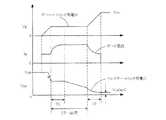
電圧駆動型スイッチングデバイスの定電流駆動は、図5に示すように、ミラー区間とミラー区間以外でゲート電流が一定であることが望ましい。ゲート電流が大きすぎると、放射ノイズが大きくなることによる問題が起こり、また、ゲート電流が小さすぎるとターンオン時のスイッチング損失の増加や制御装置からのオン指令に対してターンオン速度が遅くなることにより電圧利用率が低下し、モータ等の誘導性負荷を高出力で駆動できない問題が起こる。よってゲート電流は放射ノイズに影響しない範囲で、できるだけ大きくすることが望ましい。 As shown in FIG. 5, in the constant current drive of the voltage driven switching device, it is desirable that the gate current is constant in the mirror section and other than the mirror section. If the gate current is too large, there will be problems due to increased radiation noise, and if the gate current is too small, the switching loss will increase at turn-on and the turn-on speed will be slower with respect to the ON command from the controller. The problem is that the voltage utilization rate is reduced and inductive loads such as motors cannot be driven at high output. Therefore, it is desirable that the gate current be as large as possible without affecting the radiation noise.
ところで、特許文献1には、並列に接続する電力用半導体素子のゲート−エミッタ間閾値電圧にばらつきがあった場合でも、出力電流のアンバランスを補正する電力用半導体素子の駆動回路が提案されている。この特許文献1には、電力用半導体素子の駆動回路の具体例として、PNPトランジスタにより構成されるカレントミラー回路を、また、オン信号用トランジスタの具体例としてPch−MOSFETを、オフ信号用トランジスタの具体例としてNch−MOSFETを用いたものが開示されている。また、その変形例も開示されている。 By the way,
しかしながら、特許文献1に開示された電力用半導体素子の駆動回路では、図6に示すように、電圧駆動型スイッチングデバイスのミラー区間とミラー区間以外において定電流値が異なるため、ターンオン時におけるスイッチング損失を狙い通りに低減できない問題がある。また、ミラー区間以外で定電流値が減少するため、制御装置からの指令に素早く応答できず、電圧利用率が低下し、モータを高出力で駆動できない問題がある。以下にミラー区間とミラー区間以外で定電流値が変わるメカニズムについて説明する。 However, in the power semiconductor element drive circuit disclosed in
図7は、特許文献1に開示された定電流駆動回路(特許文献1の図6)を模式的に示した図である。図7は、IGBT1のゲート端子に接続され、駆動用パルス信号2のオン/オフゲート制御信号に基づき、IGBT1をターンオン/ターンオフさせるゲート信号を前記ゲート端子に出力するゲート駆動定電流回路を示している。 FIG. 7 is a diagram schematically illustrating the constant current driving circuit disclosed in Patent Document 1 (FIG. 6 of Patent Document 1). FIG. 7 shows a gate drive constant current circuit which is connected to the gate terminal of the
このゲート駆動定電流回路は、正電源3とGND電位4間に直列に接続された第1の抵抗5と第2の抵抗6と制御信号伝達トランジスタ7、および正電源3とIGBT1のゲート端子の間に直列に接続されたゲートオン抵抗8と定電流出力トランジスタ9を備え、定電流出力トランジスタ9のゲート端子が第1の抵抗5と第2の抵抗6の間に接続されている。なお、符号10はオフ信号用トランジスタ、符号11はオフ信号用トランジスタ10のゲート端子に接続される反転素子、符号12はIGBT1のゲート端子とオフ信号用トランジスタ10のコレクタ間に接続されるゲートオフ抵抗を示している。The gate drive constant current circuit includes a
図7の定電流駆動回路において、正電源3の電圧をVcc、第1の抵抗5の抵抗値をR1、第2の抵抗6の抵抗値をR2、ゲートオン抵抗8の抵抗値をRg、定電流出力トランジスタ9のコレクタ−ベース間容量をCCB、定電流出力トランジスタ9のベース−エミッタ間電圧をVBE、定電流出力トランジスタ9のベース電流をIB、定電流出力トランジスタ9の電流増幅率をhFE、IGBT1のゲート−エミッタ間電圧をVg、IGBT1のゲート電流をIgとしたとき、回路方程式によりIGBT1のミラー区間のゲート電流Ig(mirror)とミラー区間以外のゲート電流Igを算出する。In the constant current drive circuit of FIG. 7, the voltage of the
ミラー区間以外でのゲート電流Igを算出する。ゲート電流Igを算出するための回路方程式として、まずベース電流IBについて考える。ベース電流IBはゲート電流Igを電流増幅率hFEで割った電流とコレクタ−ベース間容量CCBを放電する電流の和となり、式(1)になる。The gate current Ig outside the mirror interval is calculated. As a circuit equation for calculating the gate current Ig, first consider the base current IB. The base current IB is the sum of the current obtained by dividing the gate current Ig by the current amplification factor hFE and the current that discharges the collector-base capacitor CCB , and is given by Equation (1).

次に、第1の抵抗5と第2の抵抗6の接続点V2について接点方程式を立てると式(2)になる。 Next, when a contact point equation is established for the connection point V2 between the
また、ゲート電流IgはRg=1としたとき、式(3)になる。 Further, when the gate current Ig is Rg = 1, Expression (3) is obtained.
式(1)から式(3)よりゲート電流Igについて解くと次のようになる。 Solving for the gate current Ig from the equations (1) to (3) gives the following.
図6に示すように、ミラー区間以外ではdVg/dtの傾きでゲート−エミッタ間電圧が上昇するため、式(4)よりミラー区間以外でゲート電流Igが減少する。 As shown in FIG. 6, since the gate-emitter voltage increases with a slope of dVg / dt outside the mirror interval, the gate current Ig decreases outside the mirror interval from Equation (4).
次に、ミラー区間のゲート電流Ig(mirror)を算出する。図6に示すように、ミラー区間では略dVg/dt=0となるため、式(4)にdVg/dt=0を代入すると式(5)になる。 Next, the gate current Ig (mirror) in the mirror section is calculated. As shown in FIG. 6, since dVg / dt = 0 in the mirror section, substituting dVg / dt = 0 into equation (4) yields equation (5).
よって、式(5)よりミラー区間ではゲート電流Ig(mirror)が増加する。 Therefore, the gate current Ig (mirror) increases in the mirror section from the equation (5).
図8は、従来の電圧駆動型スイッチングデバイスのミラー区間とミラー区間以外のゲート−エミッタ間電圧Vg、ゲート電流Ig、IGBT1のコレクタ−エミッタ間電圧VCEの模式図である。図8に示すように、ミラー区間突入後の区間T1ではゲート電流Igの増加に遅れがあるため、IGBT1のコレクタ−エミッタ間電圧VCEの下降が緩やかとなり、スイッチング損失増加の要因となっている。また、ミラー区間終了後の区間T2ではゲート電流Igが減少するため、IGBT1のコレクタ−エミッタ間電圧VCEの下降が緩やかとなり、IGBT1のコレクタ−エミッタ間電圧VCEを素早く飽和電圧VCE(sat)まで下げることができず、スイッチング損失増加や制御装置からのオン指令に対して応答性が悪化することにより電圧利用率が低下し、モータ等の誘導性負荷を高出力で駆動できない要因となっている。8, a gate other than the mirror section and a mirror section of a conventional voltage-driven switching devices - emitter voltage Vg, the collector of the gate current Ig, IGBT 1 - is a schematic view of the emitter voltage VCE. As shown in FIG. 8, there is a delay in increase of the period T1 in the gate current Ig after mirror section rush,
図9は、特許文献1に開示されたカレントミラー方式で構成された定電流駆動回路(特許文献1の図5)を模式的に示した図で、図7と同一符号は、同一または相当部分を示している。図9において、カレントミラーとする定電流出力トランジスタ9のペアのトランジスタ13が、正電源3とGND電位4間に直列に接続された第1の抵抗5と第2の抵抗6との間に接続され、前記ペアのトランジスタ13のベース端子が、定電流出力トランジスタ9のベース端子と第2の抵抗6に接続されている。 FIG. 9 is a diagram schematically showing a constant current driving circuit (FIG. 5 of Patent Document 1) configured by a current mirror system disclosed in
図9に示すカレントミラー方式の定電流駆動回路において、正電源3の電圧をVcc、第1の抵抗5の抵抗値をR1、第2の抵抗6の抵抗値をR2、ゲートオン抵抗8の抵抗値をRg、定電流出力トランジスタ9のコレクタ−ベース間容量をCCB、定電流出力トランジスタ9および前記ペアのトランジスタ13のベース−エミッタ間電圧をVBE、定電流出力トランジスタ9のベース電流をIB2、前記ペアのトランジスタ13のベース電流をIB1、定電流出力トランジスタ9および前記ペアのトランジスタ13の電流増幅率をhFE、IGBT1のゲート−エミッタ間電圧をVg、IGBT1のゲート電流をIgとしたとき、回路方程式によりIGBT1のゲート電流Igを算出する。なお、カレントミラーとするペアのトランジスタ13はワンチップ上で製造され、ほぼ同じ特性を有しているため、定電流出力トランジスタ9と前記ペアのトランジスタ13のベース−エミッタ間電圧VBEおよび電流増幅率hFEは等しいものとして考える。In the current mirror type constant current driving circuit shown in FIG. 9, the voltage of the
ゲート電流Igを算出するための回路方程式として、まずベース電流IB1、IB2について考える。前記ペアのトランジスタ13のエミッタ端子と第2の抵抗6の接続点をV3としたとき、ベース電流IB1はコレクタ電流V3/R2を電流増幅率hFEで割った電流となり、ベース電流IB2はゲート電流Igを電流増幅率hFEで割った電流とコレクタ−ベース間容量CCBを放電する電流の和となり、式(6)、(7)になる。First, base currents IB 1 and
次に、接続点V3について接点方程式を立てると式(8)になる。 Next, when a contact point equation is established for the connection point V3, Equation (8) is obtained.
また、ゲート電流Igは式(9)になる。 Further, the gate current Ig is represented by Expression (9).
式(6)から式(9)よりゲート電流Igについて解くと次のようになる。 Solving for the gate current Ig from the equations (6) to (9) gives the following.
ここで、hFE≒hFE−1とすると、次式のようになる。Here, when hFE ≈hFE −1, the following equation is obtained.
よって、前述の図7の定電流駆動回路同様、図6のようにミラー区間ではほぼdVg/dt=0となるため、カレントミラー方式にて構成された定電流駆動回路においてもミラー区間とミラー区間以外でゲート電流Igが異なる。 Accordingly, like the constant current drive circuit of FIG. 7 described above, since dVg / dt = 0 in the mirror section as shown in FIG. 6, even in the constant current drive circuit configured by the current mirror method, the mirror section and the mirror section Otherwise, the gate current Ig is different.
また、図7に示す定電流駆動回路では、回路構成部品のばらつき、温度ドリフトにより定電流設定値のばらつきが大きくなってしまう。図7の定電流駆動回路において、正電源3の電圧をVcc、第1の抵抗5の抵抗値をR1、第2の抵抗6の抵抗値をR2、ゲートオン抵抗8の抵抗値をRg、定電流出力トランジスタ9のベース−エミッタ間電圧をVBE、定電流出力トランジスタ9のベース電流IBとしたとき、IGBT1のゲート駆動の定電流設定値Igは式(10)となる。Further, in the constant current driving circuit shown in FIG. 7, the variation of the constant current setting value becomes large due to the variation of circuit components and the temperature drift. In the constant current drive circuit of FIG. 7, the voltage of the
ここで、前記ゲート駆動の定電流設定値Ig、正電源3の電圧Vcc、定電流出力トランジスタ9のベースーエミッタ間電圧VBE、第1の抵抗5の抵抗値R1、第2の抵抗6の抵抗値R2、ゲートオン抵抗8の抵抗値Rgは、定電流出力トランジスタ9のベース電流IBの影響を受けない値となっているとする。例えば、Vcc=15V、R1=20Ω、R2=130Ω、Rg=1Ω、25℃でのVBE=0.7V(typ)とすると、25℃でのIg(typ)値は、次のようになる。Here, the constant current set value Ig of the gate drive, the voltage Vcc of the
通常トランジスタのベース−エミッタ間電圧VBEは、±0.1V程度のばらつきがあり、更にVBEには−2mV/℃の温度係数を持っている。温度範囲を−30℃〜85℃として、VBEのばらつきを計算する。ばらつき最大値は−30℃、最小値は85℃の時となり、
VBE(最大値)=0.7+0.1−0.002×(−30−25)=0.91V
VBE(最小値)=0.7−0.1−0.002×(85−25)=0.48V
となる。また、正電源3の電圧Vcc=15Vも通常±1V程度のばらつきがあり、最大値16V、最小値14V程度となる。定電流駆動トランジスタ9のベース−エミッタ間電圧VBEのばらつき、正電源3の電圧Vccのばらつきを式(10)に代入して前記ゲート駆動の定電流設定値Igのばらつきを計算するとUsually, the base-emitter voltage VBE of the transistor varies about ± 0.1 V, and VBE has a temperature coefficient of −2 mV / ° C. The temperature range for -30 ° C. to 85 °C., to calculate the variation in theV BE. The maximum variation is -30 ° C and the minimum value is 85 ° C.
VBE (maximum value) = 0.7 + 0.1−0.002 × (−30−25) = 0.91V
VBE (minimum value) = 0.7−0.1−0.002 × (85−25) = 0.48V
It becomes. Further, the voltage Vcc = 15V of the
となる。よって、前記ゲート駆動の定電流設定値Igのばらつきが、
ばらつき+側=1.65A÷1.3A=+27%
ばらつき−側=0.96A÷1.3A=−26%
となり、非常に大きいばらつきを持つ。It becomes. Therefore, the variation of the constant current set value Ig of the gate drive is
Variation + side = 1.65A / 1.3A = + 27%
Variation-side = 0.96A / 1.3A = -26%
And has a very large variation.
また、上述のように、第1の抵抗5の抵抗値R1、第2の抵抗6の抵抗値R2は、定電流駆動トランジスタ9のベース電流IBの影響を受けない抵抗値に設定する必要があるため、第1の抵抗5の抵抗値R1、第2の抵抗6の抵抗値R2での電力消費が大きくなり、駆動回路の電源が大型化してしまう。Further, as described above, the resistance value R1 of the
一方、図9に示すカレントミラー方式による定電流駆動回路の場合、カレントミラーとするペアのトランジスタ13はワンチップ上で製造されほぼ同じ特性を有しているため、定電流設定値のばらつきは非常に小さい。装置の小型化、低消費電力の観点から、カレントミラー回路のミラー比は1:1とせず、1:10等その比が大きいほど望ましい。 On the other hand, in the case of the constant current driving circuit using the current mirror system shown in FIG. 9, the pair of
しかしながら、カレントミラー回路のミラー比が1:10のように大きくなると、大量生産され安価で入手できるディスクリート部品はなく、専用にカスタムICを作る必要があり、コストが高くなる要因となる。また、ゲート駆動回路は、通常専用にゲート駆動専用ICを使用する場合が多く、ゲート駆動用カスタムICにカレントミラー回路を内蔵させることも考えられるが、IGBTが大容量でゲート駆動の定電流値が大きい場合、横型構造でしかIC内部にパワートランジスタを形成できないカスタムICではチップサイズが非常に大きくなり、コストが高くなってしまう。 However, when the mirror ratio of the current mirror circuit is increased to 1:10, there is no discrete component that is mass-produced and available at low cost, and it is necessary to make a custom IC for exclusive use, which increases the cost. The gate drive circuit usually uses a dedicated gate drive IC, and it is conceivable to incorporate a current mirror circuit in the gate drive custom IC. However, the IGBT has a large capacity and a constant current value for gate drive. Is large, the chip size is very large in a custom IC in which a power transistor can be formed inside the IC only in a horizontal structure, resulting in an increase in cost.
この発明は、上述の問題を解決するためになされたものであり、ターンオン時のゲート電流を希望する電流値に高精度に設定する電圧駆動型スイッチングデバイスの駆動回路を得ることを目的とするものである。 The present invention has been made to solve the above-described problem, and an object thereof is to obtain a drive circuit for a voltage-driven switching device that sets a gate current at turn-on to a desired current value with high accuracy. It is.
この発明に係る電圧駆動型スイッチングデバイスの駆動回路は、電圧駆動型スイッチングデバイスのゲート端子に接続され、駆動用パルス信号のオン/オフゲート制御信号に基づき、前記スイッチングデバイスをターンオン/ターンオフさせるゲート信号を前記ゲート端子に出力する電圧駆動型スイッチングデバイスの駆動回路において、正電源とGND電位間に接続された定電圧ダイオードと抵抗と制御信号伝達トランジスタの直列接続体と、前記正電源と前記スイッチングデバイスのゲート端子間に接続されたゲートオン抵抗と定電流出力トランジスタの直列接続体と、を備え、前記定電流出力トランジスタのベース端子を、前記定電圧ダイオードと前記抵抗との間に接続すると共に、前記定電圧ダイオードのツェナー電圧温度係数と、前記定電流出力トランジスタのベース−エミッタ間電圧の温度係数を合わせたものである。A drive circuit for a voltage-driven switching device according to the present invention is connected to a gate terminal of the voltage-driven switching device, and receives a gate signal for turning on / off the switching device based on an on / off gate control signal of a driving pulse signal. In the drive circuit of the voltage-driven switching device that outputs to the gate terminal, a series connection body of a constant voltage diode, a resistor, and a control signal transmission transistor connected between a positive power source and a GND potential, the positive power source, and the switching device and a series connection of the connected gate-on resistor and the constant current output transistor between the gate terminal, said base terminal of the constant current output transistor,the connection between the resistor and the constant voltagediode, the constant Zener voltage temperature coefficient of voltage diode, Kijo current output transistor based - isa combination of the temperature coefficient of the emitter voltage.
この発明に係る電圧駆動型スイッチングデバイスの駆動回路によれば、ターンオン時のゲート電流を所望の電流値に高精度に設定できるため、スイッチング損失の低減が可能となる。また、定電圧ダイオードのツェナー電圧温度係数と、定電流出力トランジスタのベース−エミッタ間電圧の温度係数を合わせることにより、定電流設定値の精度が向上し、損失のばらつきを低減することができる。According to the voltage-driven switching device drive circuit of the present invention, the gate current at turn-on can be set to a desired current value with high accuracy, so that switching loss can be reduced.Further, by combining the Zener voltage temperature coefficient of the constant voltage diode and the temperature coefficient of the base-emitter voltage of the constant current output transistor, the accuracy of the constant current set value can be improved and loss variation can be reduced.
以下、添付の図面を参照して、この発明に係る電圧駆動型スイッチングデバイスのゲート駆動回路について好適な実施の形態を説明する。なお、以下では、電圧駆動型スイッチングデバイスとしてIGBTを使用する場合を例に挙げて説明するが、電圧駆動型スイッチングデバイスは、IGBTに限られることなく他の電圧駆動型スイッチングデバイス、例えば、SiC(シリコンカーバイト)デバイスを電圧駆動型スイッチングデバイスとして使用してもよい。 Preferred embodiments of a gate drive circuit for a voltage-driven switching device according to the present invention will be described below with reference to the accompanying drawings. In the following, a case where an IGBT is used as the voltage-driven switching device will be described as an example. However, the voltage-driven switching device is not limited to the IGBT, and other voltage-driven switching devices such as SiC ( Silicon carbide) devices may be used as voltage driven switching devices.
実施の形態1.
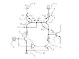
図1は、この発明の実施の形態1に係る電圧駆動型スイッチングデバイスのゲート駆動回路を示す図である。図1には、IGBT1のゲート端子に接続され、駆動用パルス信号2のオン/オフゲート制御信号に基づき、IGBT1をターンオン/ターンオフさせるゲート信号を前記ゲート端子に出力するゲート駆動定電流回路を示している。
1 is a diagram showing a gate drive circuit of a voltage-driven switching device according to
このゲート駆動定電流回路は、正電源3とGND電位4間に直列に接続された定電圧ダイオード14と前記従来技術における第2の抵抗に相当する抵抗6と制御信号伝達トランジスタ7、および正電源3とIGBT1のゲート端子間に直列に接続されたゲートオン抵抗8と定電流出力トランジスタ9を備え、定電流出力トランジスタ9のベース端子が、定
電圧ダイオード14と抵抗6の間に接続されている。なお、符号10はオフ信号用トランジスタ、符号11はオフ信号用トランジスタ10のゲート端子に接続される反転素子、符号12はIGBT1のゲート端子とオフ信号用トランジスタ10のコレクタ間に接続されるゲートオフ抵抗を示している。This gate drive constant current circuit includes a
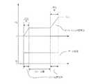
図2は、定電圧ダイオード14のツェナー電圧−ツェナー電流特性を示す図である。定電圧ダイオード14のツェナー電圧をVz、定電圧ダイオードのツェナー電流をIz、定電圧ダイオードのツェナー電圧の係数をkとしたとき、ツェナー電圧Vzとツェナー電流Izには以下の関係式が成り立つ。 FIG. 2 is a diagram illustrating a Zener voltage-zener current characteristic of the
前記実施の形態1に係る電圧駆動型スイッチングデバイスのゲート駆動回路において、正電源3の電圧をVcc、抵抗6の抵抗値をR2、ゲートオン抵抗8の抵抗値をRg、定電流出力トランジスタ9のコレクタ−ベース間容量をCCB、定電流出力トランジスタ9のベース−エミッタ間電圧をVBE、定電流出力トランジスタ9のベース電流をIB、IGBT1のゲート−エミッタ間電圧をVg、IGBT1のゲート電流をIgとしたとき、回路方程式によりIGBT1のゲート電流Igを算出する。まず、定電圧ダイオード14と抵抗15の接続点V1について接点方程式をたてると式(12)、式(13)が成り立つ。In the gate drive circuit of the voltage-driven switching device according to the first embodiment, the voltage of the
ゲート電流Igは式(14)となる。The gate current Ig is expressed by equation (14).
式(12)、式(13)よりV1を消去してIgについて解くと、式(15)となる。If V1 is eliminated from Equation (12) and Equation (13) and Ig is solved, Equation (15) is obtained.
式(11)から式(13)よりVzについて解くと、式(16)となる。Solving for Vz from Equation (11) to Equation (13) yields Equation (16).
式(16)を式(15)のVzに代入すると、式(17)となる。When Expression (16) is substituted for Vz in Expression (15), Expression (17) is obtained.
ここで、k>>1/R2より、式(17)は式(18)となる。Here, from k >> 1 / R2, Equation (17) becomes Equation (18).
k≒∞なので、式(18)は式(19)となる。Since k≈∞, Expression (18) becomes Expression (19).
よって、式(19)よりゲート電流IgはdVg/dtに関係なく一定となり、ミラー区間とミラー区間以外でIGBT1のゲート電流Igは一定となる。 Therefore, from equation (19), the gate current Ig is constant regardless of dVg / dt, and the gate current Ig of the
図3は、実施の形態1に係る電圧駆動型スイッチングデバイスのミラー区間とミラー区間以外のゲート−エミッタ間電圧Vg、ゲート電流Ig、IGBT1のコレクタ−エミッタ間電圧VCEの模式図である。図3に示すように、ミラー区間突入後の区間T1でも、ゲート電流Igが一定であるため、IGBT1のコレクタ−エミッタ間電圧VCEの下降に遅れはない。また、ミラー区間以外でもゲート電流Igが減少しないため、IGBT1のコレクタ−エミッタ間電圧VCEを素早く飽和電圧VCE(sat)まで下降させることができる。3, a gate other than the mirror section and a mirror section of the voltage-driven switching device according to the first embodiment - is a schematic view of the emitter voltage VCE - emitter voltage Vg, the collector of the gate current Ig,
以上のように、実施の形態1に係る電圧駆動型スイッチングデバイスのゲート駆動回路によれば、ミラー区間とミラー区間以外でもIGBT1のゲート電流Igを一定とすることができ、ターンオン時におけるスイッチング損失を狙い通りに低減することができる。また、ミラー区間以外でもゲート電流が減少しないため、電圧駆動型スイッチングデバイスを応答性良く駆動でき、電圧利用率も向上しモータ等の誘導性負荷を高出力で駆動できる。 As described above, according to the gate drive circuit of the voltage-driven switching device according to the first embodiment, the gate current Ig of the
また、定電圧ダイオード14のツェナー電圧温度係数と、定電流出力トランジスタ9のベース−エミッタ間電圧の温度係数を合わせることにより、定電流設定値の精度が向上し、損失のばらつきを低減することもできる。 Also, by combining the Zener voltage temperature coefficient of the
実施の形態2.
次に、この発明の実施の形態2に係る電圧駆動型スイッチングデバイスのゲート駆動回路について説明する。図4は、実施の形態2に係る電圧駆動型スイッチングデバイスのゲート駆動回路を示す図である。図4には、IGBT1のゲート端子に接続され、駆動用パルス信号2のオン/オフゲート制御信号に基づき、IGBT1をターンオン/ターンオフさせるゲート信号を前記ゲート端子に出力するゲート駆動定電流回路が示されている。このゲート駆動定電流回路は、正電源3とGND電位4間に直列に接続された第1の抵抗5と第1のトランジスタ15と第2の抵抗6と制御信号伝達トランジスタ7、および正電源3とIGBT1のゲート端子間に直列に接続されたゲートオン抵抗8と定電流出力トランジスタ9を備え、第1のトランジスタ15のベース端子は第1のトランジスタ15のコレクタ端子と短絡接続されている。
Next, a gate drive circuit for a voltage driven switching device according to
また、第1のトランジスタ15とペアとなる第2のトランジスタ16のコレクタ端子は定電流出力トランジスタ9のベース端子と接続され、第2のトランジスタ16のエミッタ端子はゲートオン抵抗8と定電流出力トランジスタ9のコレクタ端子の間に接続され、第2のトランジスタ16のベース端子は第1のトランジスタ15のコレクタ端子と第2の抵抗6の間に接続されている。なお、第1のトランジスタ15と第2のトランジスタ16は、特性の揃った、例えば同じ型名で同じ製造ロットのトランジスタが使用され、ウェハの計画投入を実施することにより、同一ウェハ、同一製造条件で製造されたことを保証する運用の実施により得られる特性の揃ったディスクリート部品のトランジスタが使用されている。 The collector terminal of the
以上のような実施の形態2に係る電圧駆動型スイッチングデバイスのゲート駆動回路において、正電源3の電圧をVcc、第1の抵抗5の抵抗値をR1、第2の抵抗9の抵抗値をR2、ゲートオン抵抗8の抵抗値をRg、第1のトランジスタ15のベース−エミッタ間電圧をVBE1、第2のトランジスタ16のベース−エミッタ間電圧をVBE2としたとき、IGBT1のゲート駆動の定電流設定値Igは式(20)となる。In the gate drive circuit of the voltage-driven switching device according to the second embodiment as described above, the voltage of the
次に、図9に示す回路における定電流設定値Igのばらつきを計算する。第1のトランジスタ15と第2のトランジスタ16の25℃でのベース−エミッタ間電圧VBE(typ)=0.7V、第1の抵抗5の抵抗値R1=13Ω、第2の抵抗6の抵抗値R2=150Ω、ゲートオン抵抗8の抵抗値Rg=1Ω、正電源3の電圧Vcc=15Vとすると、25℃でのIg(typ)は、次のようになる。Next, the variation of the constant current set value Ig in the circuit shown in FIG. 9 is calculated. The base-emitter voltage VBE (typ) at 25 ° C. of the
第1のトランジスタ15、第2のトランジスタ16のベース−エミッタ間電圧のばらつきは、±0.1V程度、温度係数−2mV/℃となっているが、第1のトランジスタ15と第2のトランジスタ16に同じ形名で同じ製造ロットのものを使用することにより、第1のトランジスタ15と第2のトランジスタ16のベース−エミッタ間電圧VBEのばらつきの相対値は非常に小さい値に抑えられ、その相対値は30mV程度となる。組み合わされる第1のトランジスタ15のベース−エミッタ間電圧VBE1、第2のトランジスタ16のベース−エミッタ間電圧VBE2の最大値、最小値は以下のようになる。
VBE1(最大値)=VBE3(最大値)−0.003=0.88V
VBE2(最大値)=0.7+0.1−0.002×(−30−25)=0.91V
VBE1(最小値)=VBE3(最小値)+0.003=0.51V
VBE2(最小値)=0.7−0.1−0.002×(85−25)=0.48V
正電源3の電圧Vcc=15Vのばらつきを±1Vとし、第1および第2のトランジスタ15、16のベース−エミッタ間電圧VBEのばらつき、正電源3の電圧Vccのばらつきを式(20)に代入して定電流設定値Igのばらつきを計算するとThe variation of the base-emitter voltage of the
VBE 1 (maximum value) = VBE 3 (maximum value) −0.003 = 0.88 V
VBE 2 (maximum value) = 0.7 + 0.1−0.002 × (−30−25) = 0.91V
VBE 1 (minimum value) = VBE 3 (minimum value) + 0.003 = 0.51V
VBE 2 (minimum value) = 0.7−0.1−0.002 × (85−25) = 0.48V
The variation of the voltage Vcc of the
となり、定電流設定値Igのばらつきが、
ばらつき+側=1.44A÷1.3A=+11%
ばらつき−側=1.16A÷1.3A=−11%
となり、従来例と比較してばらつき幅が大幅に低減される。And the variation of the constant current set value Ig is
Variation + side = 1.44A / 1.3A = + 11%
Variation-side = 1.16A / 1.3A = -11%
Thus, the variation width is greatly reduced as compared with the conventional example.
更に、第1のトランジスタ15のベース−エミッタ間電圧VBE1、第2のトランジスタ16のベース−エミッタ間電圧VBE2は、1:1のカレントミラー用として、広く一般に安価で入手可能なワンチップ上に構成されたダブルトランジスタを使用した場合、VBE1、VBE2の相対値は更に小さくなり、5mV程度まで抑えられ、この場合の定電流設定値Igのばらつきを計算すると、Moreover, the base of the first transistor 15 - emitter voltage VBE 1, the base of the second transistor 16 - emitter voltage VBE 2 is 1: for the first current mirror, widely available and inexpensive one When a double transistor configured on a chip is used, the relative values of
となり、定電流設定値Igのばらつきが、
ばらつき+側=1.42A÷1.3A=+9%
ばらつき−側=1.19A÷1.3A=−9%
となり、更に高精度化が可能となる。And the variation of the constant current set value Ig is
Variation + side = 1.42A / 1.3A = + 9%
Variation-side = 1.19A / 1.3A = -9%
Thus, higher accuracy can be achieved.
また、定電流設定値Igの精度を決定する第1のトランジスタ15、第2のトランジスタ16は小容量のトランジスタで構成できるため、チップサイズを大きくすることなく、安価にゲート駆動、保護機能を有したカスタムIC内部に取り込むことが可能であり、同一チップ上で第1のトランジスタ15と第2のトランジスタ16を構成することで、定電流設定値Igを高精度化できる。 In addition, since the
また、図9における第1の抵抗5の抵抗値R1、第2の抵抗6の抵抗値R2は、第2のトランジスタ16のベース電流の影響を受けない値とすればよく、第1の抵抗5の抵抗値R1、第2の抵抗6の抵抗値R2の抵抗値を従来技術を示す図7における第1の抵抗5の抵抗値R1、第2の抵抗6の抵抗値R2の100倍程度の値にできる。そのため、第1の抵抗5の抵抗値R1、第2の抵抗6の抵抗値R2での電力消費が少なくなり、駆動回路の低消費電力化が達成できる。 Further, the resistance value R1 of the
以上のように、実施の形態2に係る電圧駆動型スイッチングデバイスのゲート駆動回路によれば、低消費電力で、高精度な定電流値となるゲート定電流駆動回路を実現できるため、IGBT1のスイッチング損失のばらつきを大幅に低減可能となり、電力変換装置の高効率化と低コスト化に寄与できる。また、高価な専用部品を必要とせず、一般に広く安価で入手可能なディスクリート部品のみで実現できるため、駆動回路の低コスト化に寄与できる。 As described above, according to the gate drive circuit of the voltage-driven switching device according to the second embodiment, it is possible to realize a gate constant current drive circuit with a low power consumption and a highly accurate constant current value. Loss variation can be greatly reduced, contributing to higher efficiency and lower cost of the power converter. Further, since it can be realized with only discrete components that are generally widely available at low cost without requiring expensive dedicated components, it is possible to contribute to cost reduction of the drive circuit.
1 IGBT
2 駆動用パルス信号
3 正電源
4 GND電位
5 第1の抵抗
6 第2の抵抗
7 制御信号伝達トランジスタ
8 ゲートオン抵抗
9 定電流出力トランジスタ
10 オフ信号用トランジスタ
11 反転素子
12 ゲートオフ抵抗
13 定電流出力トランジスタのペアとなるトランジスタ
14 定電圧ダイオード
15 第1のトランジスタ
16 第1のトランジスタとペアになる第2のトランジスタ1 IGBT
2 Driving
Claims (3)
Translated fromJapanese正電源とGND電位間に接続された定電圧ダイオードと抵抗と制御信号伝達トランジスタの直列接続体と、
前記正電源と前記スイッチングデバイスのゲート端子間に接続されたゲートオン抵抗と定電流出力トランジスタの直列接続体と、を備え、
前記定電流出力トランジスタのベース端子を、前記定電圧ダイオードと前記抵抗との間に接続すると共に、前記定電圧ダイオードのツェナー電圧温度係数と、前記定電流出力トランジスタのベース−エミッタ間電圧の温度係数を合わせたことを特徴とする電圧駆動型スイッチングデバイスのゲート駆動回路。Drive circuit for voltage-driven switching device, connected to the gate terminal of the voltage-driven switching device, and outputs a gate signal for turning on / off the switching device to the gate terminal based on the on / off gate control signal of the driving pulse signal In
A series connection body of a constant voltage diode, a resistor, and a control signal transmission transistor connected between a positive power source and a GND potential;
A series connection of a gate-on resistance and a constant current output transistor connected between the positive power supply and the gate terminal of the switching device,
The base terminal of the constant current output transistor is connected between the constant voltage diode and the resistor,the Zener voltage temperature coefficient of the constant voltage diode, and the temperature coefficient of the base-emitter voltage of the constant current output transistor the gate drive circuit for a voltage-driven switching device, characterized inthat combined.
Priority Applications (1)
| Application Number | Priority Date | Filing Date | Title |
|---|---|---|---|
| JP2009242497AJP5069735B2 (en) | 2009-10-21 | 2009-10-21 | Driver circuit for voltage-driven switching device |
Applications Claiming Priority (1)
| Application Number | Priority Date | Filing Date | Title |
|---|---|---|---|
| JP2009242497AJP5069735B2 (en) | 2009-10-21 | 2009-10-21 | Driver circuit for voltage-driven switching device |
Related Child Applications (1)
| Application Number | Title | Priority Date | Filing Date |
|---|---|---|---|
| JP2012095223ADivisionJP2012147490A (en) | 2012-04-19 | 2012-04-19 | Drive circuit for voltage-driven switching device |
Publications (2)
| Publication Number | Publication Date |
|---|---|
| JP2011091923A JP2011091923A (en) | 2011-05-06 |
| JP5069735B2true JP5069735B2 (en) | 2012-11-07 |
Family
ID=44109644
Family Applications (1)
| Application Number | Title | Priority Date | Filing Date |
|---|---|---|---|
| JP2009242497AExpired - Fee RelatedJP5069735B2 (en) | 2009-10-21 | 2009-10-21 | Driver circuit for voltage-driven switching device |
Country Status (1)
| Country | Link |
|---|---|
| JP (1) | JP5069735B2 (en) |
Families Citing this family (4)
| Publication number | Priority date | Publication date | Assignee | Title |
|---|---|---|---|---|
| CN103620930B (en)* | 2011-06-09 | 2016-04-06 | 三菱电机株式会社 | Gate drive circuit |
| JP6169928B2 (en)* | 2013-09-12 | 2017-07-26 | 東芝シュネデール・インバータ株式会社 | Gate drive circuit and power conversion device |
| KR102240284B1 (en)* | 2014-10-23 | 2021-04-15 | 삼성디스플레이 주식회사 | Dc-dc converter and display apparatus having the same |
| CN117118032B (en)* | 2023-09-13 | 2024-05-14 | 深圳市极测科技有限公司 | Battery reverse connection preventing circuit and battery reverse connection preventing system |
Family Cites Families (4)
| Publication number | Priority date | Publication date | Assignee | Title |
|---|---|---|---|---|
| JPS5515512A (en)* | 1978-07-19 | 1980-02-02 | Hitachi Ltd | Constant voltage output circuit |
| JPS6318416A (en)* | 1986-07-10 | 1988-01-26 | Matsushita Electric Ind Co Ltd | power stabilizer |
| JP3020319B2 (en)* | 1991-07-18 | 2000-03-15 | 株式会社ユタカ電機製作所 | Rectifier circuit switching circuit |
| JP2008301618A (en)* | 2007-05-31 | 2008-12-11 | Toshiba Corp | Power conversion circuit |
- 2009
- 2009-10-21JPJP2009242497Apatent/JP5069735B2/ennot_activeExpired - Fee Related
Also Published As
| Publication number | Publication date |
|---|---|
| JP2011091923A (en) | 2011-05-06 |
Similar Documents
| Publication | Publication Date | Title |
|---|---|---|
| JP4904993B2 (en) | Drive circuit for voltage-driven element | |
| JP4382312B2 (en) | Drive control device, power conversion device, power conversion device control method, and power conversion device use method | |
| KR101970112B1 (en) | Power switching device | |
| JP4742828B2 (en) | Voltage-driven switching circuit | |
| US7737737B2 (en) | Drive circuit for voltage driven electronic element | |
| JP4915158B2 (en) | Driving device for switching element for electric power | |
| JP2007228447A (en) | Gate drive circuit for switching element | |
| JP6350301B2 (en) | Load drive control device and load drive control method | |
| TWI511448B (en) | Driving circuit of power semiconductor element | |
| JP4967568B2 (en) | Gate drive circuit for voltage driven element | |
| JP5069735B2 (en) | Driver circuit for voltage-driven switching device | |
| JP4991446B2 (en) | Power converter | |
| JP2013115931A (en) | Switching element driving circuit | |
| JP6122542B1 (en) | Active clamp circuit | |
| CN107395000A (en) | Semiconductor devices | |
| JP6104391B2 (en) | Buffer circuit | |
| JP4952112B2 (en) | Drive circuit for voltage-driven element | |
| KR101329610B1 (en) | Semiconductor device | |
| JP6847641B2 (en) | Gate drive circuit | |
| JP5630484B2 (en) | Semiconductor device | |
| JP6303060B1 (en) | Gate drive circuit | |
| JP2018078533A (en) | Power module | |
| JP2012147490A (en) | Drive circuit for voltage-driven switching device | |
| CN112994673A (en) | Semiconductor device with a plurality of semiconductor chips | |
| JPH05129917A (en) | Reverse bias control circuit for voltage-driven switching element |
Legal Events
| Date | Code | Title | Description |
|---|---|---|---|
| A977 | Report on retrieval | Free format text:JAPANESE INTERMEDIATE CODE: A971007 Effective date:20120229 | |
| A131 | Notification of reasons for refusal | Free format text:JAPANESE INTERMEDIATE CODE: A131 Effective date:20120306 | |
| A521 | Request for written amendment filed | Free format text:JAPANESE INTERMEDIATE CODE: A523 Effective date:20120419 | |
| TRDD | Decision of grant or rejection written | ||
| A01 | Written decision to grant a patent or to grant a registration (utility model) | Free format text:JAPANESE INTERMEDIATE CODE: A01 Effective date:20120801 | |
| A01 | Written decision to grant a patent or to grant a registration (utility model) | Free format text:JAPANESE INTERMEDIATE CODE: A01 | |
| A61 | First payment of annual fees (during grant procedure) | Free format text:JAPANESE INTERMEDIATE CODE: A61 Effective date:20120817 | |
| FPAY | Renewal fee payment (event date is renewal date of database) | Free format text:PAYMENT UNTIL: 20150824 Year of fee payment:3 | |
| R151 | Written notification of patent or utility model registration | Ref document number:5069735 Country of ref document:JP Free format text:JAPANESE INTERMEDIATE CODE: R151 | |
| FPAY | Renewal fee payment (event date is renewal date of database) | Free format text:PAYMENT UNTIL: 20150824 Year of fee payment:3 | |
| R250 | Receipt of annual fees | Free format text:JAPANESE INTERMEDIATE CODE: R250 | |
| R250 | Receipt of annual fees | Free format text:JAPANESE INTERMEDIATE CODE: R250 | |
| R250 | Receipt of annual fees | Free format text:JAPANESE INTERMEDIATE CODE: R250 | |
| R250 | Receipt of annual fees | Free format text:JAPANESE INTERMEDIATE CODE: R250 | |
| R250 | Receipt of annual fees | Free format text:JAPANESE INTERMEDIATE CODE: R250 | |
| R250 | Receipt of annual fees | Free format text:JAPANESE INTERMEDIATE CODE: R250 | |
| R250 | Receipt of annual fees | Free format text:JAPANESE INTERMEDIATE CODE: R250 | |
| R250 | Receipt of annual fees | Free format text:JAPANESE INTERMEDIATE CODE: R250 | |
| LAPS | Cancellation because of no payment of annual fees |