JP5068222B2 - Video display device for compensating display defects - Google Patents
Video display device for compensating display defectsDownload PDFInfo
- Publication number
- JP5068222B2 JP5068222B2JP2008154784AJP2008154784AJP5068222B2JP 5068222 B2JP5068222 B2JP 5068222B2JP 2008154784 AJP2008154784 AJP 2008154784AJP 2008154784 AJP2008154784 AJP 2008154784AJP 5068222 B2JP5068222 B2JP 5068222B2
- Authority
- JP
- Japan
- Prior art keywords
- information
- compensation
- data
- defect
- area
- Prior art date
- Legal status (The legal status is an assumption and is not a legal conclusion. Google has not performed a legal analysis and makes no representation as to the accuracy of the status listed.)
- Active
Links
Images


Classifications
- G—PHYSICS
- G09—EDUCATION; CRYPTOGRAPHY; DISPLAY; ADVERTISING; SEALS
- G09G—ARRANGEMENTS OR CIRCUITS FOR CONTROL OF INDICATING DEVICES USING STATIC MEANS TO PRESENT VARIABLE INFORMATION
- G09G3/00—Control arrangements or circuits, of interest only in connection with visual indicators other than cathode-ray tubes
- G09G3/006—Electronic inspection or testing of displays and display drivers, e.g. of LED or LCD displays
- G—PHYSICS
- G09—EDUCATION; CRYPTOGRAPHY; DISPLAY; ADVERTISING; SEALS
- G09G—ARRANGEMENTS OR CIRCUITS FOR CONTROL OF INDICATING DEVICES USING STATIC MEANS TO PRESENT VARIABLE INFORMATION
- G09G2330/00—Aspects of power supply; Aspects of display protection and defect management
- G09G2330/10—Dealing with defective pixels
- G—PHYSICS
- G09—EDUCATION; CRYPTOGRAPHY; DISPLAY; ADVERTISING; SEALS
- G09G—ARRANGEMENTS OR CIRCUITS FOR CONTROL OF INDICATING DEVICES USING STATIC MEANS TO PRESENT VARIABLE INFORMATION
- G09G3/00—Control arrangements or circuits, of interest only in connection with visual indicators other than cathode-ray tubes
- G09G3/20—Control arrangements or circuits, of interest only in connection with visual indicators other than cathode-ray tubes for presentation of an assembly of a number of characters, e.g. a page, by composing the assembly by combination of individual elements arranged in a matrix no fixed position being assigned to or needed to be assigned to the individual characters or partial characters
- G09G3/2007—Display of intermediate tones
- G09G3/2044—Display of intermediate tones using dithering
- G09G3/2051—Display of intermediate tones using dithering with use of a spatial dither pattern
- G09G3/2055—Display of intermediate tones using dithering with use of a spatial dither pattern the pattern being varied in time
Landscapes
- Engineering & Computer Science (AREA)
- Physics & Mathematics (AREA)
- Computer Hardware Design (AREA)
- General Physics & Mathematics (AREA)
- Theoretical Computer Science (AREA)
- Control Of Indicators Other Than Cathode Ray Tubes (AREA)
- Liquid Crystal Display Device Control (AREA)
- Liquid Crystal (AREA)
Description
Translated fromJapanese本発明は、映像表示装置のデータ処理回路に関するもので、特に、多様な表示欠陥をデータで補償して画質を向上できる映像表示装置に関するものである。 The present invention relates to a data processing circuit of a video display device, and more particularly to a video display device capable of improving image quality by compensating various display defects with data.
最近、映像表示装置としては、液晶表示装置(Liquid Crystal Display;LCD)、プラズマディスプレイパネル(Plasma Display Panel;PDP)、有機発光ダイオード(Organic Light Emitting Diode;OLED)表示装置などの平板表示装置が主に用いられる。 Recently, as a video display device, a flat panel display device such as a liquid crystal display (LCD), a plasma display panel (PDP), or an organic light emitting diode (OLED) display device is mainly used. Used for.
映像表示装置は、映像を表示する表示パネルを完成した後、表示欠陥を検出する検査工程を経るようになる。検査工程で表示欠陥を有するものと検出された表示パネルは、欠陥部分に対するリペア工程を経るが、リペア工程でも解決できない表示欠陥が存在している。 The video display device goes through an inspection process for detecting display defects after completing a display panel for displaying video. A display panel detected as having a display defect in the inspection process undergoes a repair process for the defective portion, but there are display defects that cannot be solved by the repair process.
表示欠陥は、主に薄膜パターン形成工程で用いられる露光装備のマルチ露光時の重複露光と、各マルチレンズの収差などによる露光量の偏差に起因する。露光量の偏差によって薄膜パターンの幅が可変になり、薄膜トランジスタの寄生容量偏差、セルギャップを維持するコラムスペーサーの高さ偏差、各信号ライン間の寄生容量偏差などが発生する。このような偏差は、表示画像で輝度偏差を誘発し、表示欠陥をもたらす。露光量の偏差による表示欠陥は、露光装備のスキャン方向によって縦線または横線形態で表示パネルに表示される。このような縦線または横線形態の表示欠陥は、工程技術の改善を通しても解決されずにいる。 The display defect is mainly caused by the overlap exposure in the multi-exposure of the exposure equipment used in the thin film pattern forming process and the deviation of the exposure amount due to the aberration of each multi-lens. The width of the thin film pattern becomes variable according to the deviation of the exposure amount, and a parasitic capacitance deviation of the thin film transistor, a height deviation of the column spacer for maintaining the cell gap, a parasitic capacitance deviation between the signal lines, and the like are generated. Such a deviation induces a luminance deviation in the display image, resulting in a display defect. Display defects due to deviations in exposure amount are displayed on the display panel in the form of vertical lines or horizontal lines depending on the scanning direction of the exposure equipment. Such display defects in the form of vertical lines or horizontal lines have not been solved through improvements in process technology.
また、表示欠陥は、異物質が流入した欠陥画素によってポイント欠陥の形態で表示される。欠陥画素に対してはリペア工程が行われるが、リペアされた画素によってもポイント欠陥が発生する。例えば、欠陥画素がリペア工程によって暗点化された場合、暗点化された画素は、ホワイト画像内でブラックポイント欠陥の形態で表示される。また、暗点化されたリペア画素を隣接した正常な画素とリンクさせるリペア工程を行った場合、正常画素に供給されたデータが、互いにリンクされたリペア画素に均一に分配されるべきであるので、リンクされた各画素は、データチャージ量不足によるポイント欠陥として表示される。 In addition, the display defect is displayed in the form of a point defect by a defective pixel into which a foreign substance flows. A repair process is performed on defective pixels, but point defects also occur due to the repaired pixels. For example, when a defective pixel is darkened by a repair process, the darkened pixel is displayed in the form of a black point defect in the white image. In addition, when a repair process is performed to link the darkened repair pixel with the adjacent normal pixel, the data supplied to the normal pixel should be uniformly distributed to the repair pixels linked to each other. Each linked pixel is displayed as a point defect due to insufficient data charge.
これによって、最近は、工程を通して解決されない表示欠陥を回路的に補償するための方法が考慮されている。しかしながら、露光量の差による横線または縦線表示欠陥が輝度分布及び欠陥位置情報の面において異なるので、従来の回路補償方法は、横線データ補償回路を縦線表示欠陥のある表示装置に適用できなく、その反対に、縦線データ補償回路を横線表示欠陥のある表示装置に適用できないという問題点がある。また、従来の回路補償方法は、欠陥領域の輝度による適応的な補償値の加減処理が不可能であった。例えば、欠陥領域が暗い状況であると仮定し、欠陥領域を周辺の正常領域より明るく輝度補正する方法を用いたり、欠陥領域が明るい欠陥である場合、正常領域をより明るく輝度補正する方法を用いることで、欠陥領域の補償値を定量化及びシステム化することが難しいという問題点がある。 As a result, recently, a method for compensating for a display defect which is not solved through a process in a circuit is considered. However, since the horizontal line or vertical line display defect due to the difference in exposure amount differs in terms of luminance distribution and defect position information, the conventional circuit compensation method cannot apply the horizontal line data compensation circuit to a display device having a vertical line display defect. On the contrary, there is a problem that the vertical line data compensation circuit cannot be applied to a display device having a horizontal line display defect. Further, the conventional circuit compensation method cannot perform adaptive compensation value adjustment processing depending on the luminance of the defective area. For example, assuming that the defect area is dark, use a method of correcting the brightness of the defect area brighter than the surrounding normal area, or use a method of correcting the brightness of the normal area brighter if the defect area is a bright defect. Thus, there is a problem that it is difficult to quantify and systematize the compensation value of the defect area.
したがって、従来の映像表示装置は、横線または縦線表示欠陥のある映像表示装置に対する区分なしに共通的に適用されるとともに、欠陥領域の位置によって適応的に補償値を加減できるデータ補償回路が要求される。また、原価節減のためにデータ補償回路の単純な構成が要求される。 Therefore, the conventional video display device is commonly applied without any distinction to the video display device having a horizontal line or vertical line display defect, and a data compensation circuit capable of adaptively adjusting the compensation value depending on the position of the defective area is required. Is done. In addition, a simple configuration of the data compensation circuit is required for cost reduction.
本発明は、上記のような従来の問題点を解決するためのもので、その目的は、多様な表示欠陥をデータで補償しながら回路構成を単純化できる映像表示装置を提供することにある。 The present invention is to solve the conventional problems as described above, and an object of the present invention is to provide a video display device capable of simplifying a circuit configuration while compensating various display defects with data.
本発明に係る映像表示装置は、表示パネル;前記表示パネルの縦線欠陥領域に表示されるデータを補償するための縦線欠陥情報を保存した第1メモリ;前記表示パネルの横線欠陥領域に表示されるデータを補償するための横線欠陥情報を保存した第2メモリ;前記第1メモリからの縦線欠陥情報を用いて前記縦線欠陥領域に表示されるデータを補償する縦線補償部と、前記第2メモリからの横線欠陥情報を用いて前記横線欠陥領域に表示されるデータを補償する横線補償部と、前記縦線または横線の方向を指示する制御情報に応答して前記縦線補償部または横線補償部の出力を選択するマルチプレクサとを含む第1補償部;前記第1補償部で補償されたデータをフレームレートコントロールディザリングを用いて空間的及び時間的に分散させる第2補償部;前記第2補償部と接続され、前記第1及び第2メモリのうち何れか一つに保存されたポイント欠陥情報を用いて前記表示パネルのポイント欠陥領域に表示されるデータを補償する第3補償部;及び前記第1乃至第2補償部によって補償されたデータを前記表示パネルに供給する駆動部を具備する。
本発明に係る映像表示装置は、映像表示装置で発生した定型欠陥領域を補償するための定型欠陥情報と、前記定型欠陥領域の方向を指示する方向情報と、ポイント欠陥領域を補償するためのポイント欠陥情報を保存したメモリと;前記メモリの定型欠陥情報を用いて前記定型欠陥領域のデータを補償する第1補償部と;前記定型欠陥補償部で補償されたデータを空間及び時間的に分散させる第2補償部と;前記メモリのポイント欠陥情報を用いて前記ポイント欠陥領域のデータを補償する第3補償部と;を備えており、前記第1補償部は、前記定型欠陥情報を縦線欠陥領域の情報として認識して入力データを補償する縦線補償部と;前記縦線補償部と前記メモリの前記定型欠陥情報を共用し、前記定型欠陥情報を横線定型欠陥領域の情報として認識して入力データを補償する横線補償部と;前記メモリの前記方向情報によって前記縦線及び横線補償部のうち何れか一つの補償部の出力データを選択して出力するマルチプレクサを具備する。
本発明に係る映像表示装置は、映像表示装置から発生した定型欠陥領域を補償するための定型欠陥情報と、前記定型欠陥領域の方向を指示する方向情報と、ポイント欠陥領域を補償するためのポイント欠陥情報とを保存したメモリと;前記メモリの定型欠陥情報を用いて前記定型欠陥領域のデータを補償する第1補償部と;前記統合補償部で補償されたデータを空間及び時間的に分散させる第2補償部と;前記メモリのポイント欠陥情報を用いて前記ポイント欠陥領域のデータを補償する第3補償部と;を備えており、前記第1補償部は、前記メモリの定型欠陥情報を縦線または横線欠陥領域の情報として認識して入力データを補償する。
本発明に係る液晶表示装置は、多数の画素を有する液晶パネルと;前記液晶パネルに発生した定型欠陥領域及びポイント欠陥領域のうち少なくとも一つの欠陥領域に表示されるデータを補償する前記データ補償回路と;前記データ補償回路で補償されたデータを整列して出力し、多数の制御信号を生成して出力するタイミングコントローラと;前記タイミングコントローラの制御に応答して前記液晶パネルを駆動するパネル駆動部と;を備えており、前記データ補償回路は、前記タイミングコントローラと一つの半導体チップの形態で具現されたことを特徴とする。An image display device according to the present invention includes: a display panel; a first memory storing vertical line defect information for compensating data displayed in the vertical line defect area of the display panel; displayed in the horizontal line defect area of the display panel. A second memory storing horizontal line defect information for compensating data to be compensated; a vertical line compensation unit for compensating data displayed in the vertical line defect area using the vertical line defect information from the first memory; A horizontal line compensation unit that compensates data displayed in the horizontal line defect region using horizontal line defect information from the second memory, and the vertical line compensation unit in response to control information that indicates a direction of the vertical line or horizontal line Or a first compensator including a multiplexer for selecting the output of the horizontal line compensator; data compensated by the first compensator is dispersed spatially and temporally using frame rate control dithering. A second compensator; data connected to the second compensator and displayed in the point defect area of the display panel using the point defect information stored in one of the first and second memories. A third compensation unit for compensating; and a drive unit for supplying data compensated by the first and second compensation units to the display panel.
A video display device according to the present invention includes fixed defect information for compensating a fixed defect region generated in the video display device, direction information indicating the direction of the fixed defect region, and points for compensating the point defect region. A memory that stores defect information; a first compensation unit that compensates for data in the fixed defect region using the fixed defect information of the memory; and data that is compensated by the fixed defect compensation unit is dispersed in space and time A second compensator; and a third compensator that compensates the data of the point defect region using the point defect information of the memory; and the first compensator converts the fixed defect information into a vertical line defect. A vertical line compensator that recognizes area information and compensates input data; and shares the fixed defect information of the vertical line compensator and the memory with the fixed defect information as horizontal line fixed defect area information. And horizontal compensation unit which recognizes and compensates for the input data; includes a multiplexer for selecting and outputting the output data of any one of the compensator of the vertical lines and the horizontal line compensator by the direction information of the memory.
A video display device according to the present invention includes fixed defect information for compensating a fixed defect region generated from the video display device, direction information indicating the direction of the fixed defect region, and points for compensating the point defect region. A memory that stores defect information; a first compensation unit that compensates the data of the fixed defect region using the fixed defect information of the memory; and the data compensated by the integrated compensation unit is dispersed in space and time A second compensator; and a third compensator that compensates the data of the point defect region using the point defect information of the memory, wherein the first compensator vertically converts the fixed defect information of the memory. The input data is compensated by recognizing the information as a line or horizontal line defect area.
A liquid crystal display device according to the present invention includes a liquid crystal panel having a large number of pixels; and the data compensation circuit for compensating data displayed in at least one defect area among a fixed defect area and a point defect area generated in the liquid crystal panel. A timing controller for aligning and outputting data compensated by the data compensation circuit and generating and outputting a large number of control signals; a panel driver for driving the liquid crystal panel in response to the control of the timing controller; The data compensation circuit is embodied in the form of the timing controller and one semiconductor chip.
本発明に係る映像表示装置のデータ補償回路は、縦線または横線の定型欠陥とポイント欠陥を同時に補償することで、表示欠陥による画質低下を効率的に改善することができる。 The data compensation circuit of the video display apparatus according to the present invention can efficiently improve the image quality degradation due to the display defect by simultaneously compensating for the vertical line or horizontal line type defect and the point defect.
また、本発明に係る映像表示装置のデータ補償回路は、第1補償部の縦線補償部及び横線補償部が一つのメモリを共用し、縦線補償部及び横線補償部の出力を定型欠陥の方向情報によって選択することで、多様な定型欠陥領域のデータを補償しながらもメモリの容量を減少させることができる。 In the data compensation circuit of the video display device according to the present invention, the vertical line compensation unit and the horizontal line compensation unit of the first compensation unit share one memory, and the outputs of the vertical line compensation unit and the horizontal line compensation unit are used for the fixed defect. By selecting according to the direction information, it is possible to reduce the memory capacity while compensating for data of various fixed defect regions.
また、本発明に係る映像表示装置のデータ補償回路は、横線補償部と縦線補償部を互いに分離せずに一つの統合補償部として構成することで、横線補償部及び縦線補償部を別個に備える場合に比べてロジック回路の大きさを減少させ、製造原価を節減することができる。 In addition, the data compensation circuit of the video display device according to the present invention is configured such that the horizontal line compensation unit and the vertical line compensation unit are configured as one integrated compensation unit without separating the horizontal line compensation unit and the vertical line compensation unit from each other. Compared with the case of preparing for, the size of the logic circuit can be reduced and the manufacturing cost can be reduced.
また、本発明に係る映像表示装置のデータ補償回路は、定型欠陥領域が明るい欠陥であるか暗い欠陥であるかによって補償データを加減し、定型結合領域の輝度差を適切に補償することができる。 In addition, the data compensation circuit of the video display device according to the present invention can appropriately compensate for the luminance difference of the fixed coupling region by adjusting the compensation data depending on whether the fixed defect region is a bright defect or a dark defect. .
また、本発明に係る映像表示装置のデータ補償回路は、第2補償部を用いて定型欠陥領域に適用された補償データを空間及び時間的に分散させ、定型欠陥領域の境界部分の輝度差を微細に補償することができ、第3補償部を用いてポイント欠陥領域の輝度差を補償することができる。 Further, the data compensation circuit of the video display device according to the present invention disperses the compensation data applied to the fixed defect area spatially and temporally using the second compensation unit, and the luminance difference at the boundary portion of the fixed defect area is obtained. It is possible to compensate finely, and it is possible to compensate for the luminance difference in the point defect region using the third compensation unit.
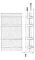
図1は、本発明の実施例に係る表示欠陥補償のための液晶表示装置を示している。 FIG. 1 shows a liquid crystal display device for display defect compensation according to an embodiment of the present invention.
図1に示した液晶表示装置は、補償回路105及びタイミングコントローラ104を含み、液晶パネル103を駆動するデータドライバー101及びゲートドライバー102をさらに含んでいる。補償回路105は、タイミングコントローラ104と一緒に一つの半導体チップの形態で具現される。 The liquid crystal display device shown in FIG. 1 includes a
補償回路105は、外部から入力されたデータR,G,Bと、多数の同期信号Vsync,Hsync,DE,DCLKを受信する。補償回路105のメモリには、規則的な横線または縦線などの定型欠陥領域に対する位置情報、階調情報及び補償データを含む定型欠陥領域の情報が保存される。また、メモリには、ポイント欠陥に対する位置情報、階調情報及び補償データを含むポイント欠陥領域の情報が保存される。補償回路105は、前記定型欠陥領域の情報を用いて定型欠陥領域に表示されるデータを補償して出力する。補償回路105は、定型欠陥領域をメイン領域と境界領域とに区分してデータを補償する(第1補償段階)。次いで、フレームレートコントロール(Frame Rate Control;以下、FRCという。)ディザリング方法を用いて定型欠陥領域の補償データを空間的及び時間的に分散させ、定型欠陥領域のデータを微細に補償する(第2補償段階)。次いで、補償回路105は、前記ポイント欠陥情報を用いてポイント欠陥領域のデータを補償して出力する(第3補償段階)。補償回路105は、補償されたデータRc,Gc,Bcと多数の同期信号Vsync,Hsync,DE,DCLKをタイミングコントローラ104に供給する。補償回路105は、正常領域に表示されるデータを補償なしにタイミングコントローラ104に供給する。補償回路105の詳細な構成に対しては、後述する。 The
タイミングコントローラ104は、補償回路105から入力されたデータRc,Gc,Bcを整列してデータドライバー101に出力し、多数の同期信号Vsync,Hsync,DE,DCLKを用いてデータドライバー101の駆動タイミングを制御するためのデータ制御信号DDCと、ゲートドライバー102の駆動タイミングを制御するためのゲート制御信号GDCを生成して出力する。 The
データドライバー101は、タイミングコントローラ104のデータ制御信号DDCに応答してタイミングコントローラ104からのデジタルデータRc,Gc,Bcをガンマ電圧を用いてアナログデータに変換し、これを液晶パネル103のデータラインに出力する。 The
ゲートドライバー102は、タイミングコントローラ104のゲート制御信号GDCに応答して液晶パネル103のゲートラインを順次的に駆動する。 The
液晶パネル103は、多数の画素が配列された画素マトリックスを通して映像を表示する。各画素は、データ信号による液晶配列の可変によって光透過率を調節する赤、緑、青のサブ画素の組み合わせで所望の色を具現する。各サブ画素は、ゲートライン17及びデータライン16と接続された薄膜トランジスタ(TFT)、薄膜トランジスタ(TFT)と並列に接続された液晶キャパシタClc及びストレージキャパシタCstを備えている。液晶キャパシタClcは、薄膜トランジスタ(TFT)を通して画素電極に供給されたデータ信号と共通電極に供給された共通電圧Vcomとの間の差電圧を充電し、充電された電圧によって液晶を駆動して光透過率を調節する。工程上、液晶パネル103に含まれる縦線または横線などの定型欠陥領域とポイント欠陥領域は、補償回路105によって補償されたデータを表示する。したがって、液晶パネル103で正常領域と欠陥領域との間の輝度差が防止されるので、画質を向上させることができる。 The
一方、補償回路105のメモリに予め保存されるべき定型欠陥領域の情報及びポイント欠陥領域の情報は、次のように設定される。 On the other hand, the fixed defect area information and the point defect area information to be stored in advance in the memory of the
表示欠陥は、露光量の偏差によって縦線または横線欠陥が規則的に表示される定型欠陥と、異物質の流入などによって不規則に表示されるポイント欠陥とに大別される。このような定型欠陥及びポイント欠陥は、映像表示装置の検査過程で検出され、検出された定型欠陥を補償するための補償データとポイント欠陥を補償するための補償データは、それぞれ設定されて補償回路105のメモリに保存される。 Display defects are broadly classified into standard defects in which vertical or horizontal line defects are regularly displayed according to the exposure amount deviation, and point defects that are irregularly displayed due to the inflow of foreign substances. Such fixed defects and point defects are detected in the inspection process of the image display device, and compensation data for compensating the detected fixed defects and compensation data for compensating the point defects are set respectively to the compensation circuit. 105 is stored in the memory.
まず、映像表示装置の輝度検査を通して縦線または横線などの定型欠陥が検出されると、定型欠陥の種類、定型欠陥領域のむら散布程度による境界領域の分割区間幅及び位置情報を設定し、定型欠陥領域のむら度合、すなわち、正常領域と欠陥領域との間の輝度差または色差を測定し、測定された輝度差または色差を補償するための補償データを設定する。 First, when a fixed defect such as a vertical line or horizontal line is detected through the luminance inspection of the image display device, the type of the fixed defect, the division area width of the boundary area according to the degree of uneven distribution of the fixed defect area, and position information are set, and the fixed defect The degree of unevenness of the area, that is, the brightness difference or color difference between the normal area and the defect area is measured, and compensation data for compensating the measured brightness difference or color difference is set.
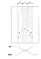
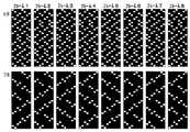
例えば、検査工程で、表示装置の定型欠陥として、図2に示すように規則的な縦線欠陥領域が検出されたり、図3に示すように規則的な横線欠陥領域が検出される。各縦線欠陥領域は、図4に示すように、縦方向に長く位置し、輝度が一定であるメイン領域C1と、メイン領域C1を基準にして両側に対称的に位置し、輝度が漸進的に可変する境界領域SG1,SG2とに区分される。また、各横線欠陥領域も、図5に示すように、横方向に長く位置するメイン領域C1と、メイン領域C1を基準にして両側に対称的に位置する境界領域SG1,SG2とに区分される。表示欠陥の境界領域SG1,SG2は、メイン領域C1と正常領域の輝度が重畳される境界領域として、メイン領域C1を基準にして対称的な多数の境界区間に分割される。境界領域SG1,SG2は、メイン領域C1側に行くほどメイン領域C1に近接した輝度を表示し、正常領域側に行くほど正常領域に近接した輝度を表示する。 For example, in the inspection process, a regular vertical line defect region as shown in FIG. 2 is detected as a fixed defect of the display device, or a regular horizontal line defect region is detected as shown in FIG. As shown in FIG. 4, each vertical line defect region is positioned long in the vertical direction and has a constant luminance, and is symmetrically positioned on both sides with respect to the main region C1, and the luminance gradually increases. Are divided into boundary regions SG1 and SG2. Further, as shown in FIG. 5, each horizontal line defect region is also divided into a main region C1 positioned long in the horizontal direction and boundary regions SG1 and SG2 positioned symmetrically on both sides with respect to the main region C1. . The display defect boundary areas SG1 and SG2 are divided into a number of boundary sections symmetrical with respect to the main area C1 as a boundary area where the luminance of the main area C1 and the normal area are superimposed. The boundary areas SG1 and SG2 display the brightness closer to the main area C1 as it goes to the main area C1, and the brightness closer to the normal area as it goes to the normal area.
定型欠陥領域は、メイン領域C1の開始位置及び幅によってメイン領域C1の位置情報が設定される。そして、境界領域SG1,SG2の位置情報は、メイン領域C1の位置情報を基準にして境界領域SG1,SG2の分割区間数及び分割区間の幅によって自動的に設定される。境界領域SG1,SG2の分割区間数及び分割区間の幅は、補償データを空間及び時間的に分散させるディザパターンの規則を逸脱しない範囲内でメイン領域C1の幅とメイン領域C1に対応する補償データの大きさによって調節される。 In the fixed defect area, the position information of the main area C1 is set according to the start position and the width of the main area C1. The position information of the boundary areas SG1 and SG2 is automatically set according to the number of divided sections and the width of the divided sections of the boundary areas SG1 and SG2 with reference to the position information of the main area C1. The number of divided sections and the width of the divided sections of the boundary areas SG1 and SG2 are within the range that does not deviate from the dither pattern rule for spatially and temporally distributing compensation data, and the compensation data corresponding to the width of the main area C1 and the main area C1. Adjusted by the size of.
定型欠陥領域のメイン領域C1と正常領域との輝度差を補償するようにメイン領域C1に対する補償データa1が設定され、対称的に位置した境界領域SG1,SG2に対する補償データb1〜e1は、漸進的に減少するように自動的に設定される。また、液晶表示装置は、図6に示すように、分割された階調区間A,B,C,D別に出力ガンマ電圧の特性が異なるので、定型欠陥領域の補償データa1〜e1は、前記ガンマ特性の異なる階調区間A,B,C,Dによって互いに異なる補償値を有するように設定される。また、定型欠陥領域の補償データa1〜e1は、表示欠陥領域の位置によって異なるように設定される。 Compensation data a1 for the main region C1 is set so as to compensate for a luminance difference between the main region C1 and the normal region of the fixed defect region, and the compensation data b1 to e1 for the boundary regions SG1 and SG2 located symmetrically are gradually increased. Automatically set to decrease. Further, as shown in FIG. 6, the liquid crystal display device has different characteristics of the output gamma voltage for each of the divided gradation sections A, B, C, and D. Therefore, the compensation data a1 to e1 for the fixed defect region are the gamma values. Different gradation values A, B, C, and D are set so as to have different compensation values. Further, the compensation data a1 to e1 for the fixed defect area are set to be different depending on the position of the display defect area.
このように、検査過程で検出された定型欠陥に対する情報、すなわち、定型欠陥の位置情報と、階調区間別に定型欠陥の位置によって最適化された補償データと、前記階調区間を指示する階調区間情報がメモリに保存される。 As described above, information on the fixed defect detected in the inspection process, that is, position information of the fixed defect, compensation data optimized by the position of the fixed defect for each gradation section, and the gradation indicating the gradation section. Section information is stored in the memory.
また、前記検査工程では、ポイント欠陥領域を検出し、検出されたポイント欠陥領域に対する位置情報と最適の補償データを設定し、設定された位置情報及び補償データをメモリに保存する。すなわち、ポイント欠陥領域の補償データは、上述した縦線または横線欠陥領域の補償データと同一の方法で、階調区間別に表示欠陥の程度によって最適化されて保存され、階調区間を指示する階調区間情報が表示装置のメモリに保存される。 In the inspection step, a point defect area is detected, position information and optimum compensation data for the detected point defect area are set, and the set position information and compensation data are stored in a memory. That is, the compensation data for the point defect area is optimized and stored according to the degree of display defect for each gradation section in the same manner as the compensation data for the vertical line or horizontal line defect area described above. Key interval information is stored in the memory of the display device.
例えば、検査工程で異物質流入などによる揮点画素が検出されると、揮点画素を信号ラインと分離させて図7に示すように暗点化し、暗点画素10を隣接した正常画素11とリンクパターン12を通してリンクさせてリペアする。この場合、ポイント欠陥は、互いにリンクされた正常画素11及び暗点画素10を含むリンク画素13によって表示される。その理由は、各リンク画素13では、正常画素11に供給されたデータが、リンクされた暗点画素10までに一様に分配されるべきであり、他の画素とリンクされていない正常画素14と対比してデータチャージ量が減少するためである。このようなデータチャージ量の減少によるポイント欠陥を補償するために、正常画素14と各リンク画素13との間、すなわち、ポイント欠陥領域と正常領域との間の輝度差または色度差を測定した後、測定された輝度差または色度差を補償できる補償データを設定する。また、ポイント欠陥領域の補償データは、階調区間別にポイント欠陥の位置によって最適化され、ポイント欠陥の位置情報及び階調区間情報と一緒にメモリに保存される。 For example, when a volatile pixel due to inflow of a different substance is detected in the inspection process, the volatile pixel is separated from the signal line and darkened as shown in FIG. The
図8は、本発明の第1実施例に係る液晶表示装置の補償回路を示している。 FIG. 8 shows a compensation circuit of the liquid crystal display device according to the first embodiment of the present invention.
図8に示した補償回路105は、前記定型欠陥情報とポイント欠陥情報が保存されたメモリ40と、メモリ40からの定型欠陥情報を用いて定型欠陥領域のデータRe,Ge,Beを補償する第1補償部30と、第1補償部30で補償されたデータRm1,Gm1,Bm1をFRCディザリング方法を用いて空間的及び時間的に分散させて微細に補償する第2補償部160と、第2補償部160と接続され、前記メモリ40からのポイント欠陥情報を用いてポイント欠陥領域のデータを補償する第3補償部170とを備えている。補償回路105は、正常領域のデータをデータ補償なしに出力する。 The
メモリ40には、上述したように、縦線及び/または横線などの定型欠陥領域の位置情報PD1、階調区間情報GD1及び補償データCD1を含む定型欠陥情報が保存される。定型欠陥領域の位置情報PD1は、各欠陥領域の開始及び終了位置情報を画素数で表す。例えば、定型欠陥領域の位置情報PD1は、定型欠陥領域に含まれたメイン領域と境界領域の各分割区間に対する開始位置情報と終了位置情報を画素数で表す。補償データCD1は、正常領域に対比する欠陥領域の輝度差または色度差を補償するためのもので、階調区間及び欠陥領域の位置によって区分されて保存される。定型欠陥領域の補償データCD1は、各定型欠陥領域のメイン領域と境界領域の各分割区間に対して最適化された補正値を含む。階調区間情報GD1は、ガンマ特性によって分割された多数の階調区間情報を指示する。また、メモリ40には、ポイント欠陥領域に対する位置情報PD2、階調区間情報GD2及び補償データCD2を含むポイント欠陥情報が保存される。 As described above, the
補償回路105は、外部からの入力データR,G,Bをビット拡張して第1補償部30に供給するビット拡張部20をさらに備えている。例えば、ビット拡張部20は、8ビットの入力データに3ビット(”000”)を下位ビットとして付加し、11ビットのデータにビット拡張し、ビット拡張されたデータRe,Ge,Beを第1補償部30に供給する。 The
第1補償部30は、メモリ40の定型欠陥情報PD1,GD1,CD1を用いて縦線または横線などの定型欠陥領域に表示される入力データRe,Ge,Beを補償して出力する。第1補償部30は、定型欠陥領域のデータに該当する補償データPD1を加減してデータを補償する。第1補償部30は、正常領域のデータを補償なしに出力する。 The
第2補償部160は、第1補償部30で補償されたデータRm1,Gm1,Bm1をFRCディザリング方法を用いて空間的及び時間的に分散させて微細に補償する。定型欠陥領域で境界領域の補償データがFRCディザリング方法によって空間的及び時間的に分散されることで、前記境界領域の輝度差が微細に補償される。例えば、第2補償部160は、第1補償部30からのデータRm1,Gm1,Bm1で補償データが適用された下位ビット部分をディザパターンを用いて空間及び時間的に分散させる。これによって、定型欠陥領域での微細な輝度差、すなわち、定型欠陥領域と正常領域との間の境界部の輝度差をさらに微細に補正することができる。 The
第3補償部170は、メモリ40に保存されたポイント欠陥情報PD2,GD2,CD2を用いてポイント欠陥領域に表示されるデータRm2,Gm2,Bm2を補償する。第3補償部170は、正常領域のデータを補償なしに出力する。 The
図9は、図8に示した第1補償部30及びメモリ40を示している。 FIG. 9 shows the
図9に示した第1補償部30は、縦線欠陥または横線欠陥を有する各表示装置に区分なしに適用されるために縦線補償部70と横線補償部80を備えており、定型欠陥が縦線であるか横線であるかによって縦線補償部70または横線補償部80の出力を選択するマルチプレクサ(以下、MUXという。)90を備えている。 The
メモリ40は、縦線補償部70と接続され、縦線欠陥情報を保存した第1メモリ42Vと、横線補償部80と接続され、横線欠陥情報を保存した第2メモリ42Hとを備えている。第1メモリ42Vは、縦線欠陥領域に対する位置情報PD1V、階調区間情報GD1V及び補償データCD1Vを保存したEEPROM(Electrically Erasable Programmable Read Only Memory)44Vと、EEPROM 44Vに保存されたデータPD1V,GD1V,CD1Vを一時的に保存して縦線補償部70に供給するレジスター46Vとを備えている。第2メモリ42Hは、横線欠陥領域に対する位置情報PD1H、階調区間情報GD1H及び補償データCD1Hを保存したEEPROM 44Hと、EEPROM 44Hに保存されたデータPD1H,GD1H,CD1Hを一時的に保存して横線補償部80に供給するレジスター46Hとを備えている。2個のEEPROM 44V,44Hは1個で具現され、2個のレジスター46V,46Hも1個で具現される。EEPROM 44V,44Hの代わりに、表示装置の解像度などの識別情報を保存したEDID(Extended Display Identification Data)ROMの一部領域を割り当てて用いることができる。また、EEPROM 44V,44Hのうち何れか一つの特定のアドレスには、定型欠陥領域が縦線欠陥であるか横線欠陥であるかを指示する定型欠陥領域の方向情報と、定型欠陥領域の有無を示して定型欠陥領域の補償可否を指示する定型欠陥補償有無情報と、ポイント欠陥領域の補償可否を指示するポイント補償有無情報とを含む制御情報CSが保存される。例えば、前記制御情報CSに割り当てられた一つのバイトのうち3ビットデータがそれぞれ前記三つの情報を表す。一方、前記制御情報CSは、前記補償回路105が内蔵されたタイミングコントローラ104の3個のオプションピンの値で設定される。 The
縦線補償部70は、縦線欠陥領域に表示される入力データRe,Ge,Beを補償するために階調判断部72、位置判断部74、補償データ選択部76及び演算器78を備えている。 The vertical
階調判断部72は、各入力データRe,Ge,Beの階調値を分析し、第1メモリ42Vから読み込んだ階調区間情報GD1Vのうち入力データRe,Ge,Beがそれぞれ含まれる階調区間情報を選択し、これを補償データ選択部76に出力する。例えば、階調区間情報GD1Vは、256階調をガンマ特性によって3個の階調区間(階調区間1:30〜70階調、階調区間2:71〜150階調、階調区間3:151〜250階調)に分割される。階調判断部72は、前記3個の階調区間情報のうち各入力データRe,Ge,Beの階調値が含まれる階調区間情報を選択して出力する。 The
位置判断部74は、垂直同期信号Vsync、水平同期信号Hsync、データイネーブル信号DE、ドットクロックDCLKのうち少なくとも一つの同期信号を用いて入力データRe,Ge,Beの横方向での画素位置を判断する。例えば、位置判断部74は、データイネーブル信号DEのイネーブル期間でドットクロックDCLKをカウンティングしながら入力データRe,Ge,Beの横方向での画素位置を判断する。そして、位置判断部74は、入力データRe,Ge,Beの画素位置を第1メモリ42Vから読み込んだ縦線欠陥領域の位置情報PD1Vと比較し、縦線欠陥領域として検出されると、該当の欠陥領域の位置情報を選択して補償データ選択部76に出力する。 The position determination unit 74 determines the pixel position in the horizontal direction of the input data Re, Ge, and Be using at least one synchronization signal among the vertical synchronization signal Vsync, the horizontal synchronization signal Hsync, the data enable signal DE, and the dot clock DCLK. To do. For example, the position determination unit 74 determines the pixel position in the horizontal direction of the input data Re, Ge, Be while counting the dot clock DCLK during the enable period of the data enable signal DE. Then, the position determination unit 74 compares the pixel position of the input data Re, Ge, and Be with the position information PD1V of the vertical line defect area read from the
補償データ選択部76は、階調判断部72で選択された階調区間情報と位置判断部74で選択された位置情報に応答して、第1メモリ46Vからの補償データCD1Vのうち各入力データRe,Ge,Beに該当する補償データを選択して出力する。すなわち、補償データ選択部76は、階調判断部72の階調区間情報によって選択した該当の階調区間内で、位置判断部74の位置情報による補償データを選択して出力する。位置情報が縦線欠陥領域のうちメイン領域を指示すると、そのメイン領域を補償するための補償データが選択されて出力され、位置情報が境界領域の各分割区間を指示すると、それら各分割区間を補償するための補償データが選択されて出力される。 In response to the gradation section information selected by the
演算器78は、各入力データRe,Ge,Beに補償データ選択部76から出力された補償データを加算または減算することで、縦線欠陥領域に表示される入力データRe,Ge,Beを補償して出力する。例えば、入力データRe,Ge,Beの各11ビットに補償データ選択部76からの8ビット補償データを加算または減算することで、入力データRe,Ge,Beを補償して出力する。 The
横線補償部80は、横線欠陥領域に表示される入力データRe,Ge,Beを補償するために階調判断部82、位置判断部84、補償データ選択部86及び演算器88を備えている。 The horizontal
階調判断部82は、各入力データRe,Ge,Beの階調値を分析し、第2メモリ42Hから読み込んだ階調区間情報GD1Hのうち入力データRe,Ge,Beがそれぞれ含まれる階調区間情報を選択し、これを補償データ選択部86に出力する。 The
位置判断部84は、垂直同期信号Vsync、水平同期信号Hsync、データイネーブル信号DE、ドットクロックDCLKのうち少なくとも一つの同期信号を用いて入力データRe,Ge,Beの縦方向での画素位置を判断する。例えば、位置判断部84は、垂直同期信号Vsyncとデータイネーブル信号DEが同時にイネーブルされた期間で水平同期信号Hsyncをカウンティングしながら入力データRe,Ge,Beの縦方向での画素位置を判断する。そして、位置判断部84は、入力データRe,Ge,Beの画素位置を第2メモリ42Hから読み込んだ横線欠陥領域の位置情報PD1Hと比較し、横線欠陥領域として検出されると、該当の欠陥領域の位置情報を選択して補償データ選択部86に出力する。 The
補償データ選択部86は、階調判断部82で選択された階調区間情報と位置判断部84で選択された位置情報に応答して、第2メモリ42Hからの補償データCD1Hのうち各入力データRe,Ge,Beに該当する補償データを選択して出力する。位置情報が横線欠陥領域のうちメイン領域を指示すると、そのメイン領域を補償するための補償データが選択されて出力され、位置情報が境界領域の各分割区間を指示すると、それら各分割区間を補償するための補償データが選択されて出力される。 The compensation
演算器88は、各入力データRe,Ge,Beに補償データ選択部86から出力された補償データを加算または減算することで、横線欠陥領域に表示される入力データRe,Ge,Beを補償して出力する。 The
MUX90は、前記制御情報CSのうち定型欠陥の方向情報に応答して縦線補償部70または横線補償部80の出力データを選択する。すなわち、MUX90は、定型欠陥の方向情報が縦線を指示する場合、縦線補償部70の出力データを選択して出力し、前記方向情報が横線を指示する場合、横線補償部80の出力データを選択して出力する。 The MUX 90 selects the output data of the vertical
このように、第1補償部30は、制御情報CSに応答して縦線または横線などの定型欠陥領域の入力データRe,Ge,Beを補償して出力する。 As described above, the
図10は、図8に示した第2補償部160を示している。 FIG. 10 shows the
図10に示した第2補償部160は、フレーム判断部162、画素位置判断部164、ディザ値選択部166及び加算器168を備えている。 The
フレーム判断部162は、第1補償部30からの多数の同期信号Vsync,Hsync,DE,DCLKのうち垂直同期信号Vsyncをカウンティングしてフレーム数を感知し、感知されたフレーム数情報をディザ値選択部166に出力する。 The
画素位置判断部164は、前記多数の同期信号Vsync,Hsync,DE,DCLKのうち少なくとも一つを用いて入力データRm1,Gm1,Bm1の画素位置を感知する。例えば、データイネーブル信号DEのイネーブル期間にドットクロックDCLKをカウンティングして入力データRm1,Gm1,Bm1の横位置を感知し、垂直同期信号Vsyncとデータイネーブル信号DEが同時にイネーブルされた期間で水平同期信号Vsyncをカウンティングして入力データRm1,Gm1,Bm1の画素縦位置を感知し、感知された画素位置情報をディザ値選択部166に出力する。 The pixel
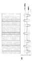
ディザ値選択部166は、第1補償部30で適用された補償データ、すなわち、第1補償部30の各出力データRm1,Gm1,Bm1の一部の下位ビットに該当する階調値と、フレーム判断部162から入力されたフレーム数情報と、画素位置判断部164から入力された画素位置情報を用いて、多数のディザパターンから該当するディザ値Dr,Dg,Dbを選択して出力する。 The dither
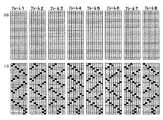
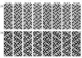
ディザ値選択部166は、設計者によって予め保存された多数のディザパターンを保存している。例えば、ディザ値選択部166は、図11A乃至図11Dに示すように、8*32の大きさを有し、0、1/8、2/8、3/8、4/8、5/8、6/8、7/8、1の階調値によってディザ値が"1"(黒い色)である画素数が漸進的に増加するように配列された多数のディザパターンをルック-アップテーブル形態で保存している(1の階調値を有するディザパターンは示していない。)。各ディザパターンの画素は"1"(黒い色)または)"0"のディザ値を有し、各ディザパターンの階調値は、ディザ値が"1"である画素数に比例して決定される。また、同一の階調値に対しても、ディザ値が"1"である各画素の位置がフレーム別に異なる、すなわち、多数のフレームFRAME1〜FRAME8で"1"の画素位置が異なる多数のディザパターンを保存している。すなわち、ディザ値選択部166は、階調別及びフレーム別に互いに異なる多数のディザパターンを保存している。各ディザパターンの大きさと各ディザパターンでディザ値が"1"である画素の位置は、設計者の必要によって多様に変化されうる。これらディザパターンによって第1補償部30で定型欠陥領域に適用された補償データが空間的及び時間的に分散されるので、定型欠陥領域の輝度差を微細に補償することができる。 The dither
第1補償部30から出力された各データRm1,Gm1,Bm1が11ビットで構成された場合、ディザ値選択部166は、前記各11ビットデータのうち下位3ビットを用いてディザ値を選択し、残りの8ビットは加算器168に出力する。ここで、3ビットは、第1補償部110で補償データが適用された部分で、正常領域に該当するデータの3ビットは"000"に設定されている。そして、ディザ値選択部166は、図11A乃至図11Dのような各ディザパターンのうち前記各入力データRm1,Gm1,Bm1の下位3ビットに該当する階調値とフレーム判断部162からのフレーム数情報に該当する一つのディザパターンを選択し、選択されたディザパターンから画素位置判断部164からの画素位置情報を用いて入力データRm1,Gm1,Bm1の各画素位置に該当する1ビットずつのディザ値Dr,Dg,Dbを選択し、これを加算器168に出力する。 When each data Rm1, Gm1, Bm1 output from the
加算器168は、ディザ値選択部166で各データRm1,Gm1,Bm1の下位3ビットと分離された上位8ビットと、ディザ値選択部166で選択されたディザ値Dr,Dg,Dbとを加算し、この結果を第3補償部170に出力する。 The
これによって、第2補償部160は、第1補償部110からの出力データRm1,Gm1,Bm1で補償データ部分をFRCディザリング方法を用いて空間及び時間的に分散させ、定型欠陥領域の輝度差を微細にさらに補償し、補償データによる画質低下を防止する。 Accordingly, the
図12は、図8に示した第3補償部170を示している。 FIG. 12 shows the
図12に示した第3補償部170は、階調判断部172、位置判断部174、補償データ選択部176及び演算器178を備えている。ポイント欠陥領域を補償するためのポイント欠陥情報PD2,GD2,CD2は、図9に示した第1及び第2メモリ42V,42Hのうち何れか一つに保存される。 The
階調判断部172は、ポイント欠陥領域のリンク画素に供給される各入力データRm2,Gm2,Bm2の階調値を分析し、第1及び第2メモリ42V,42Hのうち何れか一つからの階調区間情報GD2のうち入力データRm2,Gm2,Bm2がそれぞれ含まれる階調区間情報を選択し、これを補償データ選択部176に出力する。 The gray
位置判断部174は、外部システムから入力された垂直同期信号Vsync、水平同期信号Hsync、データイネーブル信号DE、ドットクロックDCLKのうち少なくとも一つの同期信号を用いて入力データRm2,Gm2,Bm2の画素位置を判断する。例えば、位置判断部174は、データイネーブル信号DEのイネーブル期間にドットクロックDCLKをカウンティングし、入力データRm2,Gm2,Bm2の横位置を感知し、垂直同期信号Vsyncとデータイネーブル信号DEが同時にイネーブルされた期間で水平同期信号Hsyncをカウンティングし、入力データRm2,Gm2,Bm2の画素縦位置を感知する。位置判断部174は、感知された入力データRm2,Gm2,Bm2の画素位置を第1及び第2メモリ42V,42Hのうち何れか一つからのポイント欠陥領域の位置情報PD2と比較し、ポイント欠陥領域として検出されると、感知された画素位置情報を補償データ選択部176に出力する。 The
補償データ選択部176は、階調判断部172で選択された階調区間情報と位置判断部174で選択された位置情報に応答して、第1及び第2メモリ42V,42Hのうち何れか一つからの補償データCD2のうち入力データRm2,Gm2,Bm2に該当する補償データを選択して出力する。 The compensation
演算器178は、補償データ選択部176から出力された補償データと入力データRm2,Gm2,Bm2とを加減し、その結果を出力する。 The
これによって、第3補償部170は、ポイント欠陥領域のデータRm2,Gm2,Bm2を補償して出力する。 Accordingly, the
このように、本発明の第1実施例に係る補償回路においては、第1補償部30の縦線補償部70及び横線補償部80が、各メモリ42V,42Hを用いて縦線補償部70及び横線補償部80の出力を定型欠陥の方向情報によって選択することで、定型欠陥領域の輝度差を補償することができる。また、本発明の第1実施例に係る補償回路は、第2補償部160を用いて第1補償部30で定型欠陥領域のデータに適用された補償データを空間及び時間的に分散させ、定型欠陥領域の境界部分の輝度差を微細に補償することができ、第3補償部170を用いてポイント欠陥領域の輝度差を補償することができる。 Thus, in the compensation circuit according to the first embodiment of the present invention, the vertical
図13は、本発明の第2実施例に係る液晶表示装置のデータ補償回路を示している。 FIG. 13 shows a data compensation circuit of a liquid crystal display device according to the second embodiment of the present invention.
図13に示したデータ補償回路は、定型欠陥情報PD1,CD1,GD1とポイント欠陥情報PD2,CD2,GD2が保存されたメモリ100と、メモリ100からの定型欠陥情報を用いて定型欠陥領域のデータRe,Ge,Beを補償する第1補償部110と、第1補償部110で補償されたデータRm1,Gm1,Bm1をFRCディザリング方法を用いて空間的及び時間的に分散させて微細に補償する第2補償部160と、第2補償部160と接続され、前記メモリ100からのポイント欠陥情報PD2,CD2,GD2を用いてポイント欠陥領域のデータを補償する第3補償部170とを備えている。 The data compensation circuit shown in FIG. 13 includes a
図13に示した第1補償部110は、縦線補償部120と横線補償部140が一つのメモリ100を共用するという点で、図9に示した第1補償部30と異なる。 The
露光装備のスキャン方向によって、縦線欠陥が発生する表示パネルと横線欠陥が発生する表示パネルとが区分されるので、該当の表示装置では、縦線欠陥情報または横線欠陥情報のみが用いられる。したがって、本発明では、縦線欠陥情報で使用される変数と横線欠陥情報で使用される変数とを統一し、一つのメモリ100の同一住所に縦線欠陥情報または横線欠陥情報を保存する。そして、縦線補償部120と横線補償部140が一つのメモリ100の同一住所をアクセスして並列に駆動されるが、該当の表示装置の定型欠陥が縦線欠陥であるか横線欠陥であるかによって、縦線補償部120で補償されたデータまたは横線補償部140で補償されたデータが出力される。この結果、本発明の補償回路は、縦線補償部120と横線補償部140がそれぞれのメモリを使用する場合に比べてメモリの数を減少させることができる。そして、1個のメモリを用いるとしても、縦線欠陥情報及び横線欠陥情報をそれぞれ異なる住所に保存する場合に比べてメモリの容量を減少させることができる。 Since the display panel in which the vertical line defect occurs and the display panel in which the horizontal line defect occurs are classified according to the scanning direction of the exposure equipment, only the vertical line defect information or the horizontal line defect information is used in the corresponding display device. Therefore, in the present invention, the variable used in the vertical line defect information and the variable used in the horizontal line defect information are unified, and the vertical line defect information or the horizontal line defect information is stored at the same address in one
メモリ100は、上述したように、定型欠陥情報PD1,CD1,GD1及びポイント欠陥情報PD2,CD2,GD2を保存するEEPROMと、EEPROMに保存されたデータを一時的に保存して出力するレジスターとを備えている。縦線欠陥領域で使用される変数と横線欠陥領域で使用される変数とは統一される。そして、縦線欠陥領域情報または横線欠陥領域情報は、メモリ100の同一アドレスに保存される。例えば、縦線及び横線欠陥領域に対する位置情報PD1を画素数で表し、定型欠陥が縦線であるか横線であるかを区別する定型欠陥の方向情報をメモリ100の特定のアドレスに保存したり、本発明のデータ補償回路が内蔵されたタイミングコントローラのオプションピンを用いて指示できるようにする。例えば、定型欠陥の方向情報を"0"に設定して縦線欠陥を指示し、定型欠陥の方向情報を"1"に設定して横線欠陥を指示することができる。定型欠陥の方向情報が"0"である場合、メモリ100に保存された位置情報PD1は、横線の解像度範囲内で割り当てられた画素数を用いて設定され、縦線欠陥領域の位置を指示する。定型欠陥の方向情報が"1"である場合、メモリ100に保存された位置情報PD1は、縦線解像度範囲内で割り当てられた画素数を用いて設定され、横線欠陥領域の位置を指示する。すなわち、メモリ100で設定された定型欠陥の方向情報によって、定型欠陥領域の位置情報PD1が縦線欠陥領域または横線欠陥領域の位置を指示する。 As described above, the
一方、定型欠陥領域は、図14に示すように正常領域より明るく表示されたり、図15に示すように暗く表示されたり、図16に示すように明るい欠陥領域と暗い欠陥領域とが混在された形態で表示される。補償データは、表示欠陥が明るい欠陥領域であるか暗い欠陥領域であるかによって入力データに加算(+)または減算(−)されて輝度を補償することができる。したがって、定型欠陥領域が明るい欠陥であるか暗い欠陥であるかを表す明暗情報が、欠陥領域の順序によってメモリ100に保存される。すなわち、メモリ100には、図14乃至図16のように、定型欠陥領域が正常領域と対比して明るい欠陥であるか暗い欠陥であるかを区分するために、定型欠陥領域の順序情報と一緒に定型欠陥領域の明暗情報を含む制御情報CS1が特定の位置に保存される。例えば、制御情報CS1に割り当てられた一つのバイトのうち3ビットは、定型欠陥領域の順序情報を表し、1ビットは、定型欠陥が明るい欠陥であるか暗い欠陥であるかを指示する明暗情報を表す。 On the other hand, the standard defect area is displayed brighter than the normal area as shown in FIG. 14, is displayed darker as shown in FIG. 15, or a bright defect area and a dark defect area are mixed as shown in FIG. Displayed in form. The compensation data can be added (+) or subtracted (−) to the input data to compensate the luminance depending on whether the display defect is a bright defect area or a dark defect area. Therefore, light / dark information indicating whether the fixed defect area is a bright defect or a dark defect is stored in the
また、前記定型欠陥領域が縦線欠陥であるか横線欠陥であるかを指示する定型欠陥領域の方向情報と、定型欠陥領域の有無を指示して定型欠陥領域の補償可否を指示する定型欠陥補償有無情報と、ポイント欠陥領域の補償可否を指示するポイント補償有無情報が制御情報CS2として一つのアドレスに保存される。例えば、制御情報CS2に割り当てられた一つのバイトのうち3ビットデータがそれぞれ前記三つの情報を表す。 Also, the direction information of the fixed defect area that indicates whether the fixed defect area is a vertical line defect or a horizontal line defect, and the fixed defect compensation that indicates whether or not the fixed defect area can be compensated by indicating the presence or absence of the fixed defect area Presence / absence information and point compensation presence / absence information instructing whether or not the point defect area can be compensated are stored as control information CS2 at one address. For example, 3-bit data in one byte assigned to the control information CS2 represents the three pieces of information.
一方、前記制御情報CS1,CS2は、メモリ100に保存されずに、補償回路105を内蔵したタイミングコントローラ104のオプションピンの値で設定される。 On the other hand, the control information CS1 and CS2 are not stored in the
第1補償部110には、図8に示したビット拡張部20を通してビット拡張されたデータRe,Ge,Beが入力される。第1補償部110は、メモリ100に保存された定型欠陥情報PD1,CD1,GD1を用いて縦線または横線欠陥領域の入力データRe,Ge,Beを補償して出力する。すなわち、第1補償部110は、メモリ100からの定型欠陥情報PD1,CD1,GD1に応答して、定型欠陥領域のメイン領域C1と境界領域SG1,SG2の入力データRe,Ge,Beを補償して出力する。そして、第1補償部110は、正常領域の入力データをデータ補償なしに出力する。 The
具体的に、第1補償部110は、メモリ100からの位置情報PD1を縦線欠陥領域の位置情報として用いて入力データRe,Ge,Beを補償して出力する縦線補償部120と、前記位置情報PD1を横線欠陥領域の位置情報として用いて入力データRe,Ge,Beを補償して出力する横線補償部140と、制御情報CS2の定型欠陥の方向情報によって縦線補償部120または横線補償部140の出力データを選択するMUX156とを備えている。第1補償部110は、メモリ100を共用する縦線補償部120と横線補償部140を並列に駆動し、入力データRe,Ge,Beに対する縦線補償及び横線補償を同時に行った後、MUX156を通して縦線補償部120または横線補償部140を選択して出力する。 Specifically, the
縦線補償部120は、階調判断部122、位置判断部124、補償データ選択部126、加算器128、減算器130及びMUX132,134を備えている。 The vertical
階調判断部122は、各入力データRe,Ge,Beの階調値を分析し、メモリ100から読み込んだ階調区間情報GD1のうち入力データRe,Ge,Beがそれぞれ含まれる階調区間情報を選択し、これを補償データ選択部126に出力する。 The
位置判断部124は、垂直同期信号Vsync、水平同期信号Hsync、データイネーブル信号DE、ドットクロックDCLKのうち少なくとも一つの同期信号を用いて入力データRe,Ge,Beの横方向での画素位置を判断する。例えば、位置判断部124は、データイネーブル信号DEのイネーブル期間でドットクロックDCLKをカウンティングしながら入力データRe,Ge,Beの横方向での画素位置を判断する。そして、位置判断部124は、入力データRe,Ge,Beの画素位置を第1メモリ100から読み込んだ縦線欠陥領域の位置情報PD1と比較し、縦線欠陥領域として検出されると、該当の欠陥領域の位置情報を選択して補償データ選択部126に出力する。 The
補償データ選択部126は、階調判断部122で選択された階調区間情報と位置判断部124で選択された位置情報に応答して、メモリ100からの補償データCD1のうち入力データRe,Ge,Beに該当する補償データを選択して出力する。すなわち、補償データ選択部126は、階調判断部122の階調区間情報によって選択した該当の階調区間内で、位置判断部124の位置情報による補償データを選択して出力する。位置情報が縦線欠陥領域のうちメイン領域を指示すると、そのメイン領域を補償するための補償データが選択されて出力され、位置情報が境界領域の各分割区間を指示すると、それら各分割区間を補償するための補償データが選択されて出力される。 The compensation
加算器128は、補償データ選択部126から出力された補償データと入力データRe,Ge,Beとを加算し、その結果を出力する。減算器130は、補償データ選択部126から出力された補償データを入力データRe,Ge,Beから減算し、その結果を出力する。 The
MUX132は、定型欠陥領域の明暗情報を定型欠陥領域の順序によって順次的に出力し、前記加算器128または減算器130の出力を選択するMUX134を制御する。定型欠陥領域の明暗情報は、定型欠陥領域の順序情報と一緒にメモリ100に制御情報CS1として保存されている。メモリ100から読み込んだ制御情報CS1は、定型欠陥領域の数によってMUX132に供給される。MUX132は、位置判断部124で検出される縦線欠陥領域の順序Vmによって制御情報CS1を選択し、これをMUX134に供給する。したがって、MUX134は、MUX132から供給された制御情報CS1内に含まれた明暗情報によって前記加算器128または減算器130の出力を選択し、これをMUX156に供給する。 The
横線補償部140は、階調判断部142、位置判断部144、補償データ選択部146、加算器148、減算器150及びMUX152,154を備えている。このような横線補償部140は、位置判断部144のみが回路構成において縦線補償部120と異なり、他の回路構成は、縦線補償部120と同一である。 The horizontal
階調判断部142は、各入力データRe,Ge,Beの階調値を分析し、メモリ100から読み込んだ階調区間情報GD1のうち入力データRe,Ge,Beがそれぞれ含まれる階調区間情報を選択し、これを補償データ選択部146に出力する。 The
位置判断部144は、垂直同期信号Vsync、水平同期信号Hsync、データイネーブル信号DE、ドットクロックDCLKのうち少なくとも一つの同期信号を用いて入力データRe,Ge,Beの縦方向での画素位置を判断する。例えば、位置判断部144は、垂直同期信号Vsyncとデータイネーブル信号DEが同時にイネーブルされた期間で水平同期信号Hsyncをカウンティングしながら入力データRe,Ge,Beの縦方向での画素位置を判断する。そして、位置判断部144は、入力データRe,Ge,Beの画素位置をメモリ100からの定型欠陥領域の位置情報PD1と比較し、定型欠陥領域として検出されると、該当の欠陥領域の位置情報を選択し、これを補償データ選択部146に出力する。 The
補償データ選択部146は、階調判断部142で選択された階調区間情報と位置判断部144で選択された位置情報に応答して、メモリ100からの補償データCD1のうち入力データRe,Ge,Beに該当する補償データを選択して出力する。 The compensation
加算器148は、補償データ選択部146から出力された補償データと入力データRe,Ge,Beとを加算し、その結果を出力する。減算器150は、補償データ選択部146から出力された補償データを入力データRe,Ge,Beから減算し、その結果を出力する。 The
MUX154は、制御情報CS1内の定型欠陥領域の明暗情報によって加算器148または減算器150からの出力データを選択し、これを出力する。 The
MUX152は、メモリ100から読み込んだ制御情報CS1を位置判断部144で検出される横線欠陥領域の順序Hmによって選択し、これをMUX154に供給する。したがって、MUX154は、MUX152から供給された制御情報CS1内に含まれた明暗情報によって前記加算器148または減算器150の出力を選択し、これをMUX156に供給する。 The MUX 152 selects the control information CS1 read from the
MUX156は、メモリ100からの制御情報CS2のうち定型欠陥の方向情報に応答して縦線補償部120または横線補償部140の出力データを選択する。すなわち、MUX156は、定型欠陥の方向情報が縦線を指示する場合、縦線補償部120の出力データを選択して出力し、前記方向情報が横線を指示する場合、横線補償部140の出力データを選択して出力する。 The
これによって、第1補償部110は、一つのメモリ100に保存された定型欠陥領域の情報PD1,CD1,GD1を用いて縦線または横線などの定型欠陥領域の入力データRe,Ge,Beを補償して出力する。 Accordingly, the
第2補償部160は、第1補償部110で補償されたデータRm1,Gm1,Bm1をFRCディザリング方法を用いて空間的及び時間的に分散させて微細に補償する。定型欠陥領域で境界領域の補償データがFRCディザリング方法によって空間的及び時間的に分散されることで、前記境界領域の輝度差が微細に補償される。 The
第3補償部170は、メモリ100に保存されたポイント欠陥情報PD2,GD2,CD2を用いてポイント欠陥領域に表示されるデータRm2,Gm2,Bm2を補償する。第3補償部170は、正常領域のデータを補償なしに出力する。 The
このように、本発明の第2実施例に係る補償回路は、第1補償部110の縦線補償部120及び横線補償部140が一つのメモリ100を共用し、縦線補償部120及び横線補償部140の出力を定型欠陥の方向情報によって選択することで、定型欠陥領域の輝度差を補償しながらもメモリ100の容量を減少させることができる。また、定型欠陥領域が明るい欠陥であるか暗い欠陥であるかによって補償データを加減し、定型結合領域の輝度差を適切に補償することができる。 As described above, in the compensation circuit according to the second embodiment of the present invention, the vertical
図17は、本発明の第3実施例に係る液晶表示装置のデータ補償回路を示している。 FIG. 17 shows a data compensation circuit of a liquid crystal display device according to the third embodiment of the present invention.
図17に示したデータ補償回路は、定型欠陥情報PD1,CD1,GD1とポイント欠陥情報PD2,CD2,GD2が保存されたメモリ100と、メモリ100からの定型欠陥情報PD1,CD1,GD1を用いて定型欠陥領域のデータを補償する第1補償部220と、第1補償部220で補償されたデータRm1,Gm1,Bm1をFRCディザリング方法を用いて空間的及び時間的に分散させて微細に補償する第2補償部160と、第2補償部160と接続され、前記メモリ100からのポイント欠陥情報PD2,CD2,GD2を用いてポイント欠陥領域のデータを補償する第3補償部170とを備えている。 The data compensation circuit shown in FIG. 17 uses the fixed defect information PD1, CD1, GD1 and the point defect information PD2, CD2, GD2 stored in the
図17に示した第1補償部220は、縦線及び横線の区分なしに一つの補償部として構成されるという点で、図13に示した第1補償部110と異なる。 The
メモリ100は、上述したように、定型欠陥情報PD1,CD1,GD1及びポイント欠陥情報PD2,CD2,GD2を保存するEEPROMと、EEPROMに保存されたデータを一時的に保存して出力するレジスターとを備えている。縦線欠陥領域情報または横線欠陥領域情報は、メモリ100の同一アドレスに保存される。また、メモリ100には、定型欠陥領域の順序情報と一緒に、定型欠陥領域の明暗情報を含む制御情報CS1が保存される。また、前記定型欠陥領域が縦線欠陥であるか横線欠陥であるかを指示する定型欠陥領域の方向情報と、定型欠陥領域の有無を指示して定型欠陥領域の補償可否を指示する定型欠陥補償有無情報と、ポイント欠陥領域の補償可否を指示するポイント補償有無情報が制御情報CS2として保存される。 As described above, the
第1補償部220には、図8に示したビット拡張部20を通してビット拡張されたデータRe,Ge,Beが入力される。第1補償部220は、メモリ100に保存された定型欠陥情報PD1,CD1,GD1を用いて縦線または横線欠陥領域の入力データRe,Ge,Beを補償して出力する。すなわち、第1補償部220は、メモリ100からの定型欠陥情報PD1,CD1,GD1に応答して、定型欠陥領域のメイン領域C1と境界領域SG1,SG2の入力データRe,Ge,Beを補償して出力する。そして、第1補償部110は、正常領域の入力データをデータ補償なしに出力する。 The
具体的に、第1補償部220は、階調判断部222、位置判断部224、補償データ選択部226、加算器228、減算器230及びMUX232,234を備えている。 Specifically, the
階調判断部222は、各入力データRe,Ge,Beの階調値を分析し、メモリ100から読み込んだ階調区間情報GD1のうち入力データRe,Ge,Beがそれぞれ含まれる階調区間情報を選択し、これを補償データ選択部226に出力する。 The
位置判断部224は、垂直同期信号Vsync、水平同期信号Hsync、データイネーブル信号DE、ドットクロックDCLKのうち少なくとも一つの同期信号を用いて入力データRe,Ge,Beの横方向または縦方向の画素位置を判断する。 The
具体的に、位置判断部224は、図18に示すように、入力データRe,Ge,Beの横方向での画素位置を判断する第1位置判断部322と、縦方向での画素位置を判断する第2位置判断部324と、制御情報CS2に含まれた定型欠陥の方向情報によって第1位置判断部322または第2位置判断部324の出力を選択するMUX326とを備えている。 Specifically, as shown in FIG. 18, the
第1位置判断部322は、データイネーブル信号DEのイネーブル期間でドットクロックDCLKをカウンティングしながら入力データRe,Ge,Beの横方向での画素位置を判断する。第1位置判断部322は、入力データRe,Ge,Beの画素位置をメモリ100からの定型欠陥領域位置情報PD1と比較し、定型欠陥領域として検出されると、該当の欠陥領域の位置情報を選択してMUX326に出力する。 The first
第2位置判断部324は、垂直同期信号Vsyncとデータイネーブル信号DEが同時にイネーブルされた期間で水平同期信号Hsyncをカウンティングしながら入力データRe,Ge,Beの縦方向での画素位置を判断する。第2位置判断部324は、入力データRe,Ge,Beの画素位置をメモリ100からの定型欠陥領域位置情報PD1と比較し、定型欠陥領域として検出されると、該当の欠陥領域の位置情報を選択してMUX326に出力する。 The second
MUX326は、制御情報CS2に含まれた定型欠陥の方向情報によって第1位置判断部322または第2位置判断部324から入力される定型欠陥領域の位置情報を補償データ選択部226に供給する。 The
補償データ選択部226は、階調判断部222で選択された階調区間情報と位置判断部224で選択された位置情報に応答して、メモリ100からの補償データCD1のうち入力データRe,Ge,Beに該当する補償データを選択して出力する。 The compensation
加算器228は、補償データ選択部226から出力された補償データと入力データRe,Ge,Beとを加算し、その結果を出力する。減算器230は、補償データ選択部226から出力された補償データを入力データRe,Ge,Beから減算し、その結果を出力する。 The
MUX232は、定型欠陥領域の明暗情報を定型欠陥領域の順序によって順次的に出力し、前記加算器228または減算器230の出力を選択するMUX234を制御する。定型欠陥領域の明暗情報は、定型欠陥領域の順序情報と一緒にメモリ100に制御情報CS1として保存されている。メモリ100から読み込んだ制御情報CS1は、定型欠陥領域の数によってMUX232に供給される。MUX232は、位置判断部224で検出される定型欠陥領域の順序Mによって制御情報CS1を選択し、これをMUX234に供給する。したがって、MUX234は、MUX232から供給された制御情報CS1内に含まれた明暗情報によって前記加算器228または減算器230の出力を選択し、これを第2補償部180に供給する。 The
これによって、第1補償部220は、一つのメモリ100に保存された定型欠陥領域の情報PD1,CD1,GD1を用いて縦線または横線などの定型欠陥領域の入力データRe,Ge,Beを補償して出力する。 Accordingly, the
第2補償部160は、第1補償部220で補償されたデータRm1,Gm1,Bm1をFRCディザリング方法を用いて空間的及び時間的に分散させて微細に補償する。定型欠陥領域で境界領域の補償データがFRCディザリング方法によって空間的及び時間的に分散されることで、前記境界領域の輝度差が微細に補償される。 The
第3補償部170は、メモリ100に保存されたポイント欠陥情報PD2,GD2,CD2を用いてポイント欠陥領域に表示されるデータRm2,Gm2,Bm2を補償する。第3補償部170は、正常領域のデータを補償なしに出力する。 The
このように、本発明の第3実施例に係る補償回路においては、1個の第1補償部220が、一つのメモリ100に保存された定型欠陥領域の情報PD1,CD1,GD1を用いて縦線または横線などの定型欠陥領域の入力データRe,Ge,Beを補償して出力する。したがって、本発明の第3実施例に係る補償回路は、縦線または横線などの定型欠陥領域の方向情報によって多様な定型欠陥領域のデータを補償しながらもメモリ100の容量を減少させることができる。また、第3実施例に係る補償回路は、第1補償部220が縦線補償部及び横線補償部の区分なしに一つの統合された補償部として構成されるので、ロジック回路の大きさを減少させ、製造原価を節減することができる。 As described above, in the compensation circuit according to the third embodiment of the present invention, one
一方、上述した本発明の実施例に係るデータ補償回路は、液晶表示装置のみならず、OLED、PDPなどの他の映像表示装置にも適用されうる。 On the other hand, the data compensation circuit according to the embodiment of the present invention described above can be applied not only to the liquid crystal display device but also to other video display devices such as OLED and PDP.
以上説明した内容を通して、当業者であれば、本発明の技術思想を逸脱しない範囲で多様に変更及び修正可能であることを理解できるだろう。したがって、本発明の技術的範囲は、明細書の詳細な説明に記載された内容に限定されるものでなく、特許請求の範囲によって定められるべきである。 Through the contents described above, those skilled in the art will understand that various changes and modifications can be made without departing from the technical idea of the present invention. Therefore, the technical scope of the present invention should not be limited to the contents described in the detailed description of the specification, but should be defined by the appended claims.
101 データドライバー
102 ゲートドライバー
103 液晶パネル
104 タイミングコントローラ
105 補償回路
Claims (13)
Translated fromJapanese前記表示パネルの正常領域と輝度差または色差を有する欠陥領域が、前記表示パネルの縦方向に長く位置する、縦線欠陥領域に表示される入力データを補償するための縦線欠陥情報を前記表示パネルの検査工程を通じて設定して保存した第1メモリ;
前記表示パネルの正常領域と輝度差または色差を有する欠陥領域が、前記表示パネルの横方向に長く位置する、横線欠陥領域に表示される入力データを補償するための横線欠陥情報を前記表示パネルの検査工程を通じて設定して保存した第2メモリ;
前記第1メモリからの縦線欠陥情報を用いて前記縦線欠陥領域に表示される入力データに補償データを加減して前記入力データを補償する縦線補償部と、前記第2メモリからの横線欠陥情報を用いて前記横線欠陥領域に表示される入力データに補償データを加減して前記入力データを補償する横線補償部と、前記縦方向または横方向を指示する制御情報に応答して前記縦線補償部または横線補償部の出力を選択するマルチプレクサとを含む第1補償部;
前記第1補償部で補償されたデータをフレームレートコントロールディザリングを用いて空間的及び時間的に分散させる第2補償部;
前記第2補償部と接続され、前記第1及び第2メモリのうち何れか一つに前記表示パネルの検査工程を通じて設定されて保存されたポイント欠陥情報を用いて、前記表示パネルの正常画素と輝度差または色差を有するリンク画素を含む、ポイント欠陥領域に表示される入力データに補償データを加減して前記入力データを補償する第3補償部;及び
前記第1乃至第3補償部によって補償された入力データを前記表示パネルに供給する駆動部;を備えており、
前記縦線欠陥情報は、
前記縦線欠陥領域の位置情報と、前記縦線欠陥領域の位置による補償データと、前記補償データを多数の階調区間に区分する階調区間情報とを含み、
前記横線欠陥情報は、
前記横線欠陥領域の位置情報と、前記横線欠陥領域の位置による補償データと、前記補償データを多数の階調区間に区分する階調区間情報とを含み、
前記ポイント欠陥情報は、
前記ポイント欠陥領域の位置情報と、前記ポイント欠陥領域の位置による補償データと、前記補償データを多数の階調区間に区分する階調区間情報とを含み、
前記リンク画素は、暗点画素と、前記暗点画素と互いに接続された正常画素を含むことを特徴とする映像表示装置。Display panel;
The vertical line defect information for compensating the input data displayed in the vertical line defect area, in which the defect area having a luminance difference or a color difference from the normal area of the display panel is positioned long in the vertical direction of the display panel. A first memory set and stored through the panel inspection process;
Horizontal line defect information for compensating the input data displayed in the horizontal line defect area, in which a defect area having a luminance difference or a color difference from the normal area of the display panel is positioned long in the horizontal direction of the display panel. A second memory set and stored throughout the inspection process;
A vertical line compensator for compensating the input data by adding or subtracting compensation data to the input data displayed in the vertical line defect area using the vertical line defect information from the first memory; and a horizontal line from the second memory A horizontal line compensation unit that compensates the input data by adding or subtracting compensation data to the input data displayed in the horizontal line defect area using defect information, and the vertical data or the vertical direction in response to the control information indicating the horizontal direction. A first compensation unit including a multiplexer that selects an output of the line compensation unit or the horizontal line compensation unit;
A second compensator for spatially and temporally dispersing the data compensated by the first compensator using frame rate control dithering;
A normal pixel of the display panel is connected to the second compensator using point defect information set and stored in one of the first and second memories through the inspection process of the display panel. A third compensator that compensates the input data by adding or subtracting compensation data to the input data displayed in the point defect area, including link pixels having a luminance difference or a color difference; and compensated by the first to third compensators. A drive unit for supplying the input data to the display panel;
The vertical line defect information is
Position information of the vertical line defect region, compensation data according to the position of the vertical line defect region, and gradation section information for dividing the compensation data into a plurality of gradation sections,
The horizontal line defect information is
Position information of the horizontal line defect region, compensation data according to the position of the horizontal line defect region, and gradation interval information for dividing the compensation data into a plurality of gradation intervals,
The point defect information is
Position information of the point defect region, compensation data according to the position of the point defect region, and gradation interval information for dividing the compensation data into a plurality of gradation intervals,
The link display pixel includes a dark spot pixel anda normal pixelconnected to the dark spot pixel.
前記第1メモリまたは前記第2メモリからの前記階調区間情報を用いて前記入力データに該当する階調区間情報を出力する階調判断部と;
前記第1メモリまたは前記第2メモリからの前記縦線欠陥領域または前記横線欠陥領域を含む、定型欠陥領域の位置情報を用いて前記入力データに該当する欠陥領域の位置情報を出力する位置判断部と;
前記階調判断部からの前記階調区間情報と、前記位置判断部からの該当の位置情報を用いて、前記該当のメモリからの前記欠陥領域の補償データのうち前記入力データに該当する補償データを出力する補償データ選択部と;
前記入力データに前記補償データ選択部からの補償データを加減して前記入力データを補償する演算器と;を備えることを特徴とする請求項1に記載の映像表示装置。The vertical line and horizontal line compensation units are
A gradation determination unit that outputs gradation section information corresponding to the input data using the gradation section information from the first memory or the second memory;
A position determination unit that outputs position information of a defect area corresponding to the input data using position information of a fixed defect area including the vertical line defect area or the horizontal line defect area from the first memory or the second memory. When;
Compensation data corresponding to the input data among the compensation data of the defective area from the corresponding memory using the gradation section information from the gradation determining unit and the corresponding position information from the position determining unit. A compensation data selection unit for outputting
The video display device according to claim 1, further comprising: an arithmetic unit that compensates the input data by adding or subtracting compensation data from the compensation data selection unit to the input data.
前記制御情報は、前記第1及び第2メモリのうち何れか一つに保存されるもの、及び、前記第1乃至第3補償部が内蔵されたタイミングコントローラの選択ピンによって設定されるものうち、何れか一つに設定されることを特徴とする請求項1に記載の映像表示装置。The control information includes a first bit that indicates the vertical direction or the horizontal direction, a second bit that indicates whether or not to compensate for a fixed defect area including the vertical line defect area or the horizontal line defect area, and the point defect area Including a third bit indicating whether or not
The control information is stored in any one of the first and second memories and set by a selection pin of a timing controller including the first to third compensation units. The video display device according to claim 1, wherein the video display device is set to any one.
前記縦線または横線欠陥領域のメイン領域と、そのメイン領域と正常領域との間の境界領域とに区分して前記メイン領域と境界領域それぞれに対する補償データを前記入力データに加算または減算して前記入力データを補償することを特徴とする請求項1に記載の映像表示装置。The vertical line compensation unit and the horizontal line compensation unit are:
The vertical line or horizontal line defect area is divided into a main area and a boundary area between the main area and the normal area, and compensation data for each of the main area and the boundary area is added to or subtracted from the input data. The video display device according to claim 1, wherein the input data is compensated.
前記メモリの定型欠陥情報を用いて前記定型欠陥領域の入力データに補償データを加減して前記入力データを補償する第1補償部と;
前記第1補償部で補償されたデータをフレームレートコントロールディザリングを用いて空間及び時間的に分散させる第2補償部と;
前記メモリのポイント欠陥情報を用いて前記ポイント欠陥領域のデータを補償する第3補償部と;を備えており、
前記第1補償部は、
前記定型欠陥情報を縦線欠陥領域の情報として認識して入力データを補償する縦線補償部と;
前記縦線補償部と同一の前記定型欠陥情報を共用し、前記定型欠陥情報を横線定型欠陥領域の情報として認識して入力データを補償する横線補償部と;
前記メモリの前記方向情報によって前記縦線及び横線補償部のうち何れか一つの補償部の出力データを選択して出力するマルチプレクサと;を備え、
前記リンク画素は、暗点画素と、前記暗点画素と互いに接続された正常画素を含むことを特徴とする映像表示装置のデータ補償回路。A defect area having a luminance difference or a color difference from a normal area of the video display device is a vertical line defect region positioned long in the vertical direction of the video display device, or the defective region is positioned long in the horizontal direction of the video display device. Fixed defect information for compensating a fixed defect region including a horizontal line defect region, direction information indicating whether the direction of the fixed defect region is the vertical direction or the horizontal direction, and the video display device A memory in which point defect information for compensating a point defect area is set and stored through an inspection process of the video display device, including link pixels having a luminance difference or a color difference from normal pixels;
A first compensator for compensating the input data by adding or subtracting compensation data to the input data of the fixed defect region using the fixed defect information of the memory;
A second compensator for spatially and temporally dispersing data compensated by the first compensator using frame rate control dithering;
A third compensation unit that compensates the data of the point defect region using the point defect information of the memory, and
The first compensation unit includes:
A vertical line compensator that recognizes the fixed defect information as vertical line defect area information and compensates input data;
A horizontal line compensator that shares the same fixed defect information as the vertical line compensator, recognizes the fixed defect information as horizontal line fixed defect area information, and compensates input data;
A multiplexer that selects and outputs output data of any one of the vertical line and horizontal line compensators according to the direction information of the memory;
The link compensation pixel includes a dark spot pixel anda normal pixelconnected to the dark spot pixel.
前記定型欠陥領域の位置情報は、前記定型欠陥領域のメイン領域と、前記メイン領域の両側に対称的に位置する境界領域とに区分されて保存され、
前記定型欠陥領域の補償データは、前記メイン領域に表示される入力データを補償するための補償データと、前記境界領域に表示される入力データを補償するための補償データとに区分されて保存され、前記境界領域の補償データは、前記メイン領域の補償データから漸進的に減少するように設定されることを特徴とする請求項5に記載の映像表示装置のデータ補償回路。The fixed defect information includes position information of the fixed defect region, compensation data based on the position of the fixed defect region, and gradation region information that divides the compensation data into a plurality of gradation regions,
The position information of the fixed defect region is stored in a state of being divided into a main region of the fixed defect region and a boundary region positioned symmetrically on both sides of the main region,
Compensation data for the fixed defect area is divided and stored as compensation data for compensating the input data displayed in the main area and compensation data for compensating the input data displayed in the boundary area. 6. The data compensation circuit for a video display device according to claim 5, wherein the compensation data of the boundary region is set so as to gradually decrease from the compensation data of the main region.
前記メモリからの前記階調領域情報を用いて前記入力データに該当する階調領域情報を出力する階調判断部と;
前記メモリからの前記定型欠陥領域の位置情報を用いて前記入力データに該当する欠陥領域の位置情報を出力する位置判断部と;
前記階調判断部からの前記階調領域情報と、前記位置判断部からの該当の位置情報を用いて、前記メモリからの前記定型欠陥領域の補償データのうち前記入力データに該当する補償データを出力する補償データ選択部と;を備えており、
前記縦線補償部の位置判断部は、
前記定型欠陥領域の位置情報を縦線欠陥領域に対する横方向の位置情報として認識し、前記入力データに該当する横方向の画素位置を検出し、前記検出された画素位置に該当する定型欠陥領域の位置情報を出力し、
前記横線補償部の位置判断部は、
前記定型欠陥領域の位置情報を横線欠陥領域に対する横方向の位置情報として認識し、前記入力データに該当する縦方向の画素位置を検出し、前記検出された画素位置に該当する定型欠陥領域の位置情報を出力することを特徴とする請求項6に記載の映像表示装置のデータ補償回路。The vertical line and horizontal line compensation units are
A gradation determination unit that outputs gradation area information corresponding to the input data using the gradation area information from the memory;
A position determination unit that outputs position information of a defect area corresponding to the input data using position information of the fixed defect area from the memory;
Compensation data corresponding to the input data among the compensation data of the fixed defect region from the memory using the gradation region information from the gradation determination unit and the corresponding position information from the position determination unit. A compensation data selection unit to output; and
The position determination unit of the vertical line compensation unit is
Recognizing position information of the fixed defect area as position information in the horizontal direction with respect to the vertical line defect area, detecting a horizontal pixel position corresponding to the input data, and detecting a fixed defect area corresponding to the detected pixel position Output location information,
The position determination unit of the horizontal line compensation unit is
Recognizing the position information of the fixed defect area as position information in the horizontal direction with respect to the horizontal line defect area, detecting the vertical pixel position corresponding to the input data, and the position of the fixed defect area corresponding to the detected pixel position 7. The data compensation circuit for a video display device according to claim 6, wherein information is output.
前記位置判断部は、前記入力データに該当する前記定型欠陥領域を検出され、前記検出された定型欠陥領域の順序を検出して出力し、
前記縦線及び横線補償部は、
前記補償データ選択部から出力された補償データを前記入力データと加算する加算器と;
前記補償データを前記入力データから減算する減算器と;
前記位置判断部から検出された前記定型欠陥領域の順序によって前記メモリからの前記定型欠陥領域の順序情報及び明暗情報を選択的に出力するマルチプレクサと;
前記マルチプレクサで選択された定型欠陥領域の配列順序情報及び明暗情報によって前記加算器及び減算器のうち何れか一つの出力を選択するマルチプレクサと;をさらに備えることを特徴とする請求項7に記載の映像表示装置のデータ補償回路。The memory corresponds to the order in which the fixed defect areas are located in the video display device, with brightness information indicating whether the fixed defect area is a bright defect or a dark defect as compared with a normal area, Save additionally along with the order information of the standard defect area,
The position determination unit detects the fixed defect area corresponding to the input data, detects the order of the detected fixed defect area, and outputs it,
The vertical line and horizontal line compensation units are
An adder for adding the compensation data output from the compensation data selector to the input data;
A subtractor for subtracting the compensation data from the input data;
A multiplexer that selectively outputs order information and brightness information of the fixed defect area from the memory according to the order of the fixed defect area detected from the position determination unit;
The multiplexer according to claim 7, further comprising: a multiplexer that selects one output of the adder and the subtracter according to arrangement order information and brightness information of the fixed defect region selected by the multiplexer. Data compensation circuit for video display device.
前記メモリの定型欠陥情報を用いて前記定型欠陥領域の入力データに補償データを加減して前記入力データを補償する第1補償部と;
前記第1補償部で補償されたデータをフレームレートコントロールディザリングを用いて空間及び時間的に分散させる第2補償部と;
前記メモリのポイント欠陥情報を用いて前記ポイント欠陥領域のデータを補償する第3補償部と;を備えており、
前記第1補償部は、
前記メモリの定型欠陥情報を縦線または横線欠陥領域の情報として認識して入力データを補償し、
前記第1補償部は、
前記メモリからの前記階調領域情報を用いて前記入力データに該当する階調領域情報を出力する階調判断部と;
前記メモリからの前記定型欠陥領域の位置情報と前記メモリまたは外部からの選択ピンを通して入力される定型欠陥の方向情報によって、前記入力データに該当する欠陥領域の位置情報を出力する位置判断部と;
前記階調判断部からの前記階調領域情報と前記位置判断部からの該当の位置情報を用いて、前記メモリからの前記欠陥領域の補償データのうち前記入力データに該当する補償データを出力する補償データ選択部と;を備え、
前記位置判断部は、
前記入力データの横方向での画素位置を判断する第1位置判断部;
前記入力データの縦方向での画素位置を判断する第2位置判断部;及び
前記定型欠陥の方向情報によって前記第1位置判断部または第2位置判断部の出力を選択するマルチプレクサを備え、
前記リンク画素は、暗点画素と、前記暗点画素と互いに接続された正常画素を含むことを特徴とする映像表示装置のデータ補償回路。A defect area having a luminance difference or a color difference with the video display device is a vertical line defect area positioned long in the vertical direction of the video display apparatus, or a horizontal line defect area where the defect area is positioned long in the horizontal direction of the video display apparatus. Fixed defect information for compensating a fixed defect region, direction information indicating whether a direction of the fixed defect region is the vertical direction or the horizontal direction, and normal pixels of the video display device, Point defect information for compensating for the point defect area including link pixels having luminance difference or color difference is set and stored through the inspection process of the video display device, and thefixed defect information is position information of the fixed defect area And a memoryincluding compensation data based on a position of the fixed defect region, and gradation region information for dividing the compensation data into a plurality of gradation regions ;
A first compensator for compensating the input data by adding or subtracting compensation data to the input data of the fixed defect region using the fixed defect information of the memory;
A second compensator for spatially and temporally dispersing data compensated by the first compensator using frame rate control dithering;
A third compensation unit that compensates the data of the point defect region using the point defect information of the memory, and
The first compensation unit includes:
Recognizing the fixed defect information of the memory as vertical line or horizontal line defect area information to compensate the input data,
The first compensation unit includes:
A gradation determination unit that outputs gradation area information corresponding to the input data using the gradation area information from the memory;
A position determination unit that outputs position information of the defect area corresponding to the input data based on position information of the fixed defect area from the memory and direction information of the fixed defect input through the selection pin from the memory or the outside;
Compensation data corresponding to the input data among the compensation data of the defective area from the memory is output using the gradation area information from the gradation determination section and the corresponding position information from the position determination section. A compensation data selection unit;
The position determination unit
A first position determining unit that determines a pixel position in a horizontal direction of the input data;
A second position determination unit that determines a pixel position in the vertical direction of the input data; and a multiplexer that selects an output of the first position determination unit or the second position determination unit according to direction information of the fixed defect,
The link compensation pixel includes a dark spot pixel anda normal pixelconnected to the dark spot pixel.
前記定型欠陥領域の位置情報は、前記定型欠陥領域のメイン領域と、前記メイン領域の両側に対称的に位置する境界領域とに区分されて保存され、
前記定型欠陥領域の補償データは、前記メイン領域に表示される入力データを補償するための補償データと、前記境界領域に表示される入力データを補償するための補償データとに区分されて保存され、前記境界領域の補償データは、前記メイン領域の補償データから漸進的に減少するように設定されることを特徴とする請求項10に記載の映像表示装置のデータ補償回路。The fixed defect information includes position information of the fixed defect region, compensation data according to the position of the fixed defect region, and gradation region information for dividing the compensation data into a plurality of gradation regions,
The position information of the fixed defect region is stored in a state of being divided into a main region of the fixed defect region and a boundary region positioned symmetrically on both sides of the main region,
Compensation data for the fixed defect area is divided and stored as compensation data for compensating the input data displayed in the main area and compensation data for compensating the input data displayed in the boundary area. 11. The data compensation circuit for a video display device according to claim 10, wherein the compensation data of the boundary region is set so as to gradually decrease from the compensation data of the main region.
前記位置判断部は、前記入力データに該当する前記定型欠陥領域を検出され、前記検出された定型欠陥領域の順序を検出して出力し、
前記第1補償部は、
前記補償データ選択部から出力された補償データを前記入力データと加算する加算器と;
前記補償データを前記入力データから減算する減算器と;
前記位置判断部から検出された定型欠陥領域の順序情報によって前記メモリからの前記定型欠陥領域の順序情報及び明暗情報を選択的に出力するマルチプレクサと;
前記マルチプレクサで選択された定型欠陥領域の順序情報及び明暗情報によって前記加算器及び減算器のうち何れか一つの出力を選択するマルチプレクサと;をさらに備えることを特徴とする請求項11に記載の映像表示装置のデータ補償回路。The memory corresponds to the order in which the fixed defect areas are located in the video display device, with brightness information indicating whether the fixed defect area is a bright defect or a dark defect as compared with a normal area, Save additionally along with the order information of the standard defect area,
The position determination unit detects the fixed defect area corresponding to the input data, detects the order of the detected fixed defect area, and outputs it,
The first compensation unit includes:
An adder for adding the compensation data output from the compensation data selector to the input data;
A subtractor for subtracting the compensation data from the input data;
A multiplexer that selectively outputs order information and brightness information of the fixed defect area from the memory according to the order information of the fixed defect area detected from the position determination unit;
The video of claim 11, further comprising: a multiplexer that selects an output of either the adder or the subtracter according to order information and brightness information of the fixed defect area selected by the multiplexer. Data compensation circuit for display device.
前記液晶パネルに発生した前記定型欠陥領域及び前記ポイント欠陥領域のうち少なくとも一つの欠陥領域に表示されるデータを補償する請求項5乃至請求項12のうち何れか1項に記載されたデータ補償回路と;
前記データ補償回路で補償されたデータを整列して出力し、多数の制御信号を生成して出力するタイミングコントローラと;
前記タイミングコントローラの制御に応答して前記液晶パネルを駆動するパネル駆動部と;を備えており、
前記データ補償回路は、
前記タイミングコントローラと一つの半導体チップの形態で具現されたことを特徴とする液晶表示装置。A liquid crystal panel having a large number of pixels;
The data compensation circuit according to any one of claims 5 to 12, which compensates data displayed in at least one defect area among the fixed defect area and the point defect area generated in the liquid crystal panel. When;
A timing controller for aligning and outputting data compensated by the data compensation circuit and generating and outputting a number of control signals;
A panel drive unit that drives the liquid crystal panel in response to the control of the timing controller;
The data compensation circuit includes:
A liquid crystal display device implemented in the form of the timing controller and one semiconductor chip.
Applications Claiming Priority (8)
| Application Number | Priority Date | Filing Date | Title |
|---|---|---|---|
| KR20070058492 | 2007-06-14 | ||
| KR10-2007-0058492 | 2007-06-14 | ||
| KR10-2007-0111217 | 2007-11-01 | ||
| KR20070111217 | 2007-11-01 | ||
| KR1020080014842AKR101296655B1 (en) | 2007-11-01 | 2008-02-19 | Circuit of compensating data in video display device and method thereof |
| KR10-2008-0014842 | 2008-02-19 | ||
| KR10-2008-0030827 | 2008-04-02 | ||
| KR1020080030827AKR101286537B1 (en) | 2007-06-14 | 2008-04-02 | Video display device for compensating display defect |
Publications (2)
| Publication Number | Publication Date |
|---|---|
| JP2008310329A JP2008310329A (en) | 2008-12-25 |
| JP5068222B2true JP5068222B2 (en) | 2012-11-07 |
Family
ID=40131811
Family Applications (1)
| Application Number | Title | Priority Date | Filing Date |
|---|---|---|---|
| JP2008154784AActiveJP5068222B2 (en) | 2007-06-14 | 2008-06-13 | Video display device for compensating display defects |
Country Status (3)
| Country | Link |
|---|---|
| US (1) | US10810918B2 (en) |
| JP (1) | JP5068222B2 (en) |
| CN (1) | CN101354872B (en) |
Families Citing this family (28)
| Publication number | Priority date | Publication date | Assignee | Title |
|---|---|---|---|---|
| KR100586669B1 (en)* | 2003-08-27 | 2006-06-08 | 닛뽕빅터 가부시키가이샤 | Transmission system |
| CN101587696B (en)* | 2009-05-07 | 2011-09-14 | 福州华映视讯有限公司 | Response time compensation device of color sequential display |
| JP2011039451A (en)* | 2009-08-18 | 2011-02-24 | Sharp Corp | Display device, luminance unevenness correction method, and device and method for generating correction data |
| JP5059092B2 (en)* | 2009-12-15 | 2012-10-24 | シャープ株式会社 | Display device, luminance unevenness correction method, and correction data creation device |
| KR101073266B1 (en)* | 2010-02-11 | 2011-10-12 | 삼성모바일디스플레이주식회사 | Organic Light Emitting Display Device and Driving Method Thereof |
| KR20130087927A (en)* | 2012-01-30 | 2013-08-07 | 삼성디스플레이 주식회사 | Apparatus for processing image signal and method thereof |
| KR102023940B1 (en)* | 2012-12-27 | 2019-11-04 | 엘지디스플레이 주식회사 | Driving circuit of display device and method for driving the same |
| KR102090706B1 (en)* | 2012-12-28 | 2020-03-19 | 삼성디스플레이 주식회사 | Display device, Optical compensation system and Optical compensation method thereof |
| CN103489420A (en)* | 2013-09-03 | 2014-01-01 | 深圳市华星光电技术有限公司 | Method for driving liquid crystal panel, liquid crystal display device and method for compensating light spots |
| US9202423B2 (en) | 2013-09-03 | 2015-12-01 | Shenzhen China Star Optoelectronics Technology Co., Ltd | LCD device, driving method of LCD panel, and mura compensating method |
| KR102156774B1 (en)* | 2013-12-30 | 2020-09-17 | 엘지디스플레이 주식회사 | Repair Method Of Organic Light Emitting Display |
| KR102270207B1 (en)* | 2014-11-27 | 2021-06-29 | 삼성디스플레이 주식회사 | Display apparatus and method of driving the same |
| KR20160072344A (en)* | 2014-12-12 | 2016-06-23 | 삼성디스플레이 주식회사 | Organic light emitting display apparatus and driving method thereof |
| KR102387784B1 (en) | 2014-12-29 | 2022-04-15 | 엘지디스플레이 주식회사 | Organic light emitting diode display device and method for repairing thereof |
| CN104464637B (en)* | 2014-12-29 | 2017-02-22 | 深圳市华星光电技术有限公司 | Grey scale compensation method and system for defect of display panel |
| KR20170037774A (en)* | 2015-09-25 | 2017-04-05 | 삼성디스플레이 주식회사 | Data driver and display device including the same |
| EP3239929B1 (en)* | 2016-04-27 | 2019-06-12 | Canon Kabushiki Kaisha | Image processing apparatus, image processing method and program |
| JP6932944B2 (en)* | 2017-02-20 | 2021-09-08 | 株式会社リコー | Camera shake correction drive signal control device, camera shake correction device and imaging device |
| TWI626642B (en)* | 2017-06-20 | 2018-06-11 | 友達光電股份有限公司 | Display device and gamma curve compensation circuit and driving method thereof |
| CN107358935B (en)* | 2017-08-25 | 2019-12-31 | 惠科股份有限公司 | Optimization mode and equipment for brightness compensation data quantity |
| US10380975B2 (en) | 2017-08-25 | 2019-08-13 | HKC Corporation Limited | Optimization method and device for brightness compensation data volume |
| KR102441479B1 (en)* | 2017-12-27 | 2022-09-13 | 삼성디스플레이 주식회사 | Display device and method of driving display device |
| CN108597434A (en)* | 2018-04-28 | 2018-09-28 | 深圳市华星光电技术有限公司 | Show the method for adjustment of picture |
| TWI714056B (en)* | 2019-04-17 | 2020-12-21 | 奇景光電股份有限公司 | Timing controller and operating method thereof |
| KR102650708B1 (en)* | 2020-03-20 | 2024-03-25 | 삼성디스플레이 주식회사 | Display apparatus and method of driving the same |
| KR102800078B1 (en) | 2020-06-22 | 2025-04-29 | 삼성디스플레이 주식회사 | Apparatus for testing display device and display device for performing mura compensation and mura compensation method |
| US12027117B2 (en) | 2020-09-25 | 2024-07-02 | Apple Inc. | Pixel screening and repair |
| KR102257370B1 (en)* | 2020-10-15 | 2021-05-31 | 삼성전자주식회사 | An electronic device including display with varying size of screen and a method compensating degradation of the display |
Family Cites Families (14)
| Publication number | Priority date | Publication date | Assignee | Title |
|---|---|---|---|---|
| JP3672586B2 (en)* | 1994-03-24 | 2005-07-20 | 株式会社半導体エネルギー研究所 | Correction system and operation method thereof |
| JPH1062734A (en) | 1996-08-22 | 1998-03-06 | Sony Corp | Method of correcting defective pixel of liquid crystal display and defective pixel correction device |
| JP3161393B2 (en) | 1997-11-28 | 2001-04-25 | 日本電気株式会社 | Active matrix type liquid crystal display |
| JP2001075523A (en) | 2000-07-10 | 2001-03-23 | Semiconductor Energy Lab Co Ltd | Correction system and its operating method |
| JP3473600B2 (en)* | 2000-12-01 | 2003-12-08 | セイコーエプソン株式会社 | Liquid crystal display device, image data correction circuit, image data correction method, and electronic device |
| JP4549762B2 (en) | 2004-07-13 | 2010-09-22 | シャープ株式会社 | Image signal processing apparatus and method |
| JP4222340B2 (en)* | 2004-09-22 | 2009-02-12 | ソニー株式会社 | Image display device and brightness correction method in image display device |
| KR100780943B1 (en)* | 2005-09-21 | 2007-12-03 | 삼성전자주식회사 | Display integrated circuit and display driving method |
| KR101136286B1 (en) | 2005-10-17 | 2012-04-19 | 엘지디스플레이 주식회사 | Flat Display Apparatus And Picture Quality Controling Method Thereof |
| KR101127843B1 (en)* | 2005-10-25 | 2012-03-21 | 엘지디스플레이 주식회사 | Flat Display Apparatus And Picture Quality Controling Method Thereof |
| KR101137856B1 (en) | 2005-10-25 | 2012-04-20 | 엘지디스플레이 주식회사 | Flat Display Apparatus And Picture Quality Controling Method Thereof |
| KR101201314B1 (en)* | 2005-11-16 | 2012-11-14 | 엘지디스플레이 주식회사 | Method of Fabricating Flat Display Panel |
| KR101186049B1 (en)* | 2005-12-02 | 2012-09-25 | 엘지디스플레이 주식회사 | Flat Display Panel, Fabricating Method thereof, Fabricating Apparatus thereof, Picture Quality Controlling Method thereof, Picture Quality Controlling Apparatus |
| KR101264718B1 (en)* | 2007-04-02 | 2013-05-16 | 엘지디스플레이 주식회사 | Method and Apparatus for Compensating Display Defect of Flat Display |
- 2008
- 2008-06-03USUS12/155,396patent/US10810918B2/enactiveActive
- 2008-06-12CNCN2008101114288Apatent/CN101354872B/enactiveActive
- 2008-06-13JPJP2008154784Apatent/JP5068222B2/enactiveActive
Also Published As
| Publication number | Publication date |
|---|---|
| US20080309602A1 (en) | 2008-12-18 |
| JP2008310329A (en) | 2008-12-25 |
| US10810918B2 (en) | 2020-10-20 |
| CN101354872A (en) | 2009-01-28 |
| CN101354872B (en) | 2011-06-29 |
Similar Documents
| Publication | Publication Date | Title |
|---|---|---|
| JP5068222B2 (en) | Video display device for compensating display defects | |
| CN101599244B (en) | Video display capable of compensating for display defects | |
| JP4555259B2 (en) | Flat panel display and image quality control method thereof | |
| JP4787081B2 (en) | Flat panel display and image quality control method thereof | |
| US7791572B2 (en) | Flat display panel, picture quality controlling apparatus and method thereof | |
| JP5302518B2 (en) | Flat panel display and data multiplex modulation method thereof | |
| JP4881367B2 (en) | Video display device | |
| KR101274707B1 (en) | Compensation circuit of video display device for compensating display defect and method thereof | |
| US8189017B2 (en) | Apparatus and method for controlling picture quality of flat panel display | |
| KR20070044711A (en) | Flat Panel Display and Image Quality Control Method | |
| KR101675852B1 (en) | Video display device for compensating defect | |
| TWI405171B (en) | Video display device capable of compensating for display defects | |
| KR101329074B1 (en) | Apparatus And Method For Controling Picture Quality of Flat Panel Display | |
| KR101296655B1 (en) | Circuit of compensating data in video display device and method thereof | |
| KR101611919B1 (en) | Method of generating compensation region for compensating defect and video display device using the same | |
| KR101286537B1 (en) | Video display device for compensating display defect |
Legal Events
| Date | Code | Title | Description |
|---|---|---|---|
| A131 | Notification of reasons for refusal | Free format text:JAPANESE INTERMEDIATE CODE: A131 Effective date:20110314 | |
| A521 | Request for written amendment filed | Free format text:JAPANESE INTERMEDIATE CODE: A523 Effective date:20110614 | |
| A131 | Notification of reasons for refusal | Free format text:JAPANESE INTERMEDIATE CODE: A131 Effective date:20111205 | |
| A521 | Request for written amendment filed | Free format text:JAPANESE INTERMEDIATE CODE: A523 Effective date:20120305 | |
| A131 | Notification of reasons for refusal | Free format text:JAPANESE INTERMEDIATE CODE: A131 Effective date:20120326 | |
| A521 | Request for written amendment filed | Free format text:JAPANESE INTERMEDIATE CODE: A523 Effective date:20120626 | |
| TRDD | Decision of grant or rejection written | ||
| A01 | Written decision to grant a patent or to grant a registration (utility model) | Free format text:JAPANESE INTERMEDIATE CODE: A01 Effective date:20120717 | |
| A01 | Written decision to grant a patent or to grant a registration (utility model) | Free format text:JAPANESE INTERMEDIATE CODE: A01 | |
| A61 | First payment of annual fees (during grant procedure) | Free format text:JAPANESE INTERMEDIATE CODE: A61 Effective date:20120814 | |
| FPAY | Renewal fee payment (event date is renewal date of database) | Free format text:PAYMENT UNTIL: 20150824 Year of fee payment:3 | |
| R150 | Certificate of patent or registration of utility model | Free format text:JAPANESE INTERMEDIATE CODE: R150 Ref document number:5068222 Country of ref document:JP Free format text:JAPANESE INTERMEDIATE CODE: R150 | |
| R250 | Receipt of annual fees | Free format text:JAPANESE INTERMEDIATE CODE: R250 | |
| R250 | Receipt of annual fees | Free format text:JAPANESE INTERMEDIATE CODE: R250 | |
| R250 | Receipt of annual fees | Free format text:JAPANESE INTERMEDIATE CODE: R250 | |
| R250 | Receipt of annual fees | Free format text:JAPANESE INTERMEDIATE CODE: R250 | |
| R250 | Receipt of annual fees | Free format text:JAPANESE INTERMEDIATE CODE: R250 | |
| R250 | Receipt of annual fees | Free format text:JAPANESE INTERMEDIATE CODE: R250 | |
| R250 | Receipt of annual fees | Free format text:JAPANESE INTERMEDIATE CODE: R250 | |
| R250 | Receipt of annual fees | Free format text:JAPANESE INTERMEDIATE CODE: R250 | |
| R250 | Receipt of annual fees | Free format text:JAPANESE INTERMEDIATE CODE: R250 | |
| R250 | Receipt of annual fees | Free format text:JAPANESE INTERMEDIATE CODE: R250 | |
| R250 | Receipt of annual fees | Free format text:JAPANESE INTERMEDIATE CODE: R250 |