JP5061884B2 - Battery pack - Google Patents
Battery packDownload PDFInfo
- Publication number
- JP5061884B2 JP5061884B2JP2007330580AJP2007330580AJP5061884B2JP 5061884 B2JP5061884 B2JP 5061884B2JP 2007330580 AJP2007330580 AJP 2007330580AJP 2007330580 AJP2007330580 AJP 2007330580AJP 5061884 B2JP5061884 B2JP 5061884B2
- Authority
- JP
- Japan
- Prior art keywords
- voltage
- temperature
- secondary battery
- comparator
- circuit
- Prior art date
- Legal status (The legal status is an assumption and is not a legal conclusion. Google has not performed a legal analysis and makes no representation as to the accuracy of the status listed.)
- Active
Links
- 238000001514detection methodMethods0.000claimsdescription112
- HBBGRARXTFLTSG-UHFFFAOYSA-NLithium ionChemical compound[Li+]HBBGRARXTFLTSG-UHFFFAOYSA-N0.000description45
- 229910001416lithium ionInorganic materials0.000description45
- 238000010586diagramMethods0.000description14
- 230000004048modificationEffects0.000description8
- 238000012986modificationMethods0.000description8
- 239000003990capacitorSubstances0.000description3
- 230000007423decreaseEffects0.000description3
- 230000000903blocking effectEffects0.000description2
- 101100102624Drosophila melanogaster Vinc geneProteins0.000description1
- 101100112673Rattus norvegicus Ccnd2 geneProteins0.000description1
- 230000003247decreasing effectEffects0.000description1
- 229910044991metal oxideInorganic materials0.000description1
- 150000004706metal oxidesChemical class0.000description1
- 239000004065semiconductorSubstances0.000description1
Images


Classifications
- H—ELECTRICITY
- H02—GENERATION; CONVERSION OR DISTRIBUTION OF ELECTRIC POWER
- H02J—CIRCUIT ARRANGEMENTS OR SYSTEMS FOR SUPPLYING OR DISTRIBUTING ELECTRIC POWER; SYSTEMS FOR STORING ELECTRIC ENERGY
- H02J7/00—Circuit arrangements for charging or depolarising batteries or for supplying loads from batteries
- H02J7/0029—Circuit arrangements for charging or depolarising batteries or for supplying loads from batteries with safety or protection devices or circuits
- H02J7/0031—Circuit arrangements for charging or depolarising batteries or for supplying loads from batteries with safety or protection devices or circuits using battery or load disconnect circuits
- H—ELECTRICITY
- H01—ELECTRIC ELEMENTS
- H01M—PROCESSES OR MEANS, e.g. BATTERIES, FOR THE DIRECT CONVERSION OF CHEMICAL ENERGY INTO ELECTRICAL ENERGY
- H01M10/00—Secondary cells; Manufacture thereof
- H01M10/05—Accumulators with non-aqueous electrolyte
- H01M10/052—Li-accumulators
- H01M10/0525—Rocking-chair batteries, i.e. batteries with lithium insertion or intercalation in both electrodes; Lithium-ion batteries
- H—ELECTRICITY
- H01—ELECTRIC ELEMENTS
- H01M—PROCESSES OR MEANS, e.g. BATTERIES, FOR THE DIRECT CONVERSION OF CHEMICAL ENERGY INTO ELECTRICAL ENERGY
- H01M10/00—Secondary cells; Manufacture thereof
- H01M10/42—Methods or arrangements for servicing or maintenance of secondary cells or secondary half-cells
- H01M10/425—Structural combination with electronic components, e.g. electronic circuits integrated to the outside of the casing
- H—ELECTRICITY
- H01—ELECTRIC ELEMENTS
- H01M—PROCESSES OR MEANS, e.g. BATTERIES, FOR THE DIRECT CONVERSION OF CHEMICAL ENERGY INTO ELECTRICAL ENERGY
- H01M10/00—Secondary cells; Manufacture thereof
- H01M10/42—Methods or arrangements for servicing or maintenance of secondary cells or secondary half-cells
- H01M10/44—Methods for charging or discharging
- H01M10/443—Methods for charging or discharging in response to temperature
- H—ELECTRICITY
- H01—ELECTRIC ELEMENTS
- H01M—PROCESSES OR MEANS, e.g. BATTERIES, FOR THE DIRECT CONVERSION OF CHEMICAL ENERGY INTO ELECTRICAL ENERGY
- H01M10/00—Secondary cells; Manufacture thereof
- H01M10/42—Methods or arrangements for servicing or maintenance of secondary cells or secondary half-cells
- H01M10/46—Accumulators structurally combined with charging apparatus
- H—ELECTRICITY
- H01—ELECTRIC ELEMENTS
- H01M—PROCESSES OR MEANS, e.g. BATTERIES, FOR THE DIRECT CONVERSION OF CHEMICAL ENERGY INTO ELECTRICAL ENERGY
- H01M10/00—Secondary cells; Manufacture thereof
- H01M10/42—Methods or arrangements for servicing or maintenance of secondary cells or secondary half-cells
- H01M10/48—Accumulators combined with arrangements for measuring, testing or indicating the condition of cells, e.g. the level or density of the electrolyte
- H01M10/486—Accumulators combined with arrangements for measuring, testing or indicating the condition of cells, e.g. the level or density of the electrolyte for measuring temperature
- H—ELECTRICITY
- H02—GENERATION; CONVERSION OR DISTRIBUTION OF ELECTRIC POWER
- H02J—CIRCUIT ARRANGEMENTS OR SYSTEMS FOR SUPPLYING OR DISTRIBUTING ELECTRIC POWER; SYSTEMS FOR STORING ELECTRIC ENERGY
- H02J7/00—Circuit arrangements for charging or depolarising batteries or for supplying loads from batteries
- H02J7/0029—Circuit arrangements for charging or depolarising batteries or for supplying loads from batteries with safety or protection devices or circuits
- H02J7/00302—Overcharge protection
- H—ELECTRICITY
- H02—GENERATION; CONVERSION OR DISTRIBUTION OF ELECTRIC POWER
- H02J—CIRCUIT ARRANGEMENTS OR SYSTEMS FOR SUPPLYING OR DISTRIBUTING ELECTRIC POWER; SYSTEMS FOR STORING ELECTRIC ENERGY
- H02J7/00—Circuit arrangements for charging or depolarising batteries or for supplying loads from batteries
- H02J7/0029—Circuit arrangements for charging or depolarising batteries or for supplying loads from batteries with safety or protection devices or circuits
- H02J7/00304—Overcurrent protection
- H—ELECTRICITY
- H02—GENERATION; CONVERSION OR DISTRIBUTION OF ELECTRIC POWER
- H02J—CIRCUIT ARRANGEMENTS OR SYSTEMS FOR SUPPLYING OR DISTRIBUTING ELECTRIC POWER; SYSTEMS FOR STORING ELECTRIC ENERGY
- H02J7/00—Circuit arrangements for charging or depolarising batteries or for supplying loads from batteries
- H02J7/0029—Circuit arrangements for charging or depolarising batteries or for supplying loads from batteries with safety or protection devices or circuits
- H02J7/00306—Overdischarge protection
- Y—GENERAL TAGGING OF NEW TECHNOLOGICAL DEVELOPMENTS; GENERAL TAGGING OF CROSS-SECTIONAL TECHNOLOGIES SPANNING OVER SEVERAL SECTIONS OF THE IPC; TECHNICAL SUBJECTS COVERED BY FORMER USPC CROSS-REFERENCE ART COLLECTIONS [XRACs] AND DIGESTS
- Y02—TECHNOLOGIES OR APPLICATIONS FOR MITIGATION OR ADAPTATION AGAINST CLIMATE CHANGE
- Y02E—REDUCTION OF GREENHOUSE GAS [GHG] EMISSIONS, RELATED TO ENERGY GENERATION, TRANSMISSION OR DISTRIBUTION
- Y02E60/00—Enabling technologies; Technologies with a potential or indirect contribution to GHG emissions mitigation
- Y02E60/10—Energy storage using batteries
Landscapes
- Engineering & Computer Science (AREA)
- Chemical & Material Sciences (AREA)
- Manufacturing & Machinery (AREA)
- Chemical Kinetics & Catalysis (AREA)
- Electrochemistry (AREA)
- General Chemical & Material Sciences (AREA)
- Power Engineering (AREA)
- Materials Engineering (AREA)
- Microelectronics & Electronic Packaging (AREA)
- Charge And Discharge Circuits For Batteries Or The Like (AREA)
- Secondary Cells (AREA)
- Protection Of Static Devices (AREA)
Description
Translated fromJapanese本発明は、電池パックに関し、二次電池の過充電、過放電、過電流を検出して前記二次電池と負荷又は充電装置との間の配線に設けられたスイッチ素子をオフする保護回路を備えた電池パックに関する。 The present invention relates to a battery pack, and includes a protection circuit that detects overcharge, overdischarge, and overcurrent of a secondary battery and turns off a switch element provided in a wiring between the secondary battery and a load or a charging device. The present invention relates to a provided battery pack.
近年、二次電池としてリチウムイオン電池がデジタルカメラなど携帯機器に搭載されている。リチウムイオン電池は過充電及び過放電に弱いため、過充電及び過放電の保護回路を備えた電池パックの形態で使用される。 In recent years, lithium ion batteries as secondary batteries have been mounted on portable devices such as digital cameras. Lithium ion batteries are vulnerable to overcharge and overdischarge, and are therefore used in the form of a battery pack having an overcharge and overdischarge protection circuit.
図10及び図11は、従来の電池パックの各例のブロック図を示す。図10において、リチウムイオン電池2と並列に抵抗R1とコンデンサC1の直列回路が接続されている。リチウムイオン電池2の正極は電池パック1の外部端子3に接続され、負極は電流遮断用のnチャネルMOS(金属酸化膜半導体)トランジスタM1、M2を介して電池パック1の外部端子4に接続されている。 10 and 11 show block diagrams of examples of conventional battery packs. In FIG. 10, a series circuit of a resistor R <b> 1 and a capacitor C <b> 1 is connected in parallel with the
MOSトランジスタM1、M2はドレインを共通接続され、MOSトランジスタM1のソースはリチウムイオン電池2の負極に接続され、MOSトランジスタM2のソースは外部端子4に接続されている。また、MOSトランジスタM1、M2それぞれは、ドレイン・ソース間に等価的にボディダイオードD1、D2が接続されている。 The drains of the MOS transistors M 1 and
保護IC(集積回路)5は、過充電検出回路、過放電検出回路、過電流検出回路を内蔵している。また、保護IC5はリチウムイオン電池2の正極から抵抗R1を通して電源Vddを供給されると共にリチウムイオン電池2の負極から電源Vssを供給されて動作する。 The protection IC (integrated circuit) 5 includes an overcharge detection circuit, an overdischarge detection circuit, and an overcurrent detection circuit. Further, the protection IC 5 operates by being supplied with the power source Vdd from the positive electrode of the
保護IC5は過放電検出回路或いは過電流検出回路で過放電或いは過電流を検出したときDOUT出力をローレベルとしてMOSトランジスタM1を遮断し、過充電検出回路で過充電を検出したときCOUT出力をローレベルとしてMOSトランジスタM2を遮断する。 The protection IC 5 shuts down the MOS transistor M1 by setting the DOUT output to the low level when the overdischarge or overcurrent is detected by the overdischarge detection circuit or the overcurrent detection circuit, and sets the COUT output to the low level when the overcharge detection circuit detects the overcharge. As a level, the MOS transistor M2 is cut off.
図11では、更に、電池パック1内にサーミスタR3が設けられている。サーミスタR3の一端は電池パック1の端子6に接続され、他端は外部端子4に接続されている。電池パック1の端子6には充電時に充電装置から分圧抵抗を介して所定電圧が印加される。電池パック1の温度によってサーミスタR3の抵抗値が変化することで端子6の電圧は変化する。充電装置は、端子6の電圧を検出して電池パック1の温度が所定値を超えると充電を停止するよう制御を行う。 In FIG. 11, a thermistor R <b> 3 is further provided in the battery pack 1. One end of the thermistor R <b> 3 is connected to the terminal 6 of the battery pack 1, and the other end is connected to the external terminal 4. A predetermined voltage is applied to the terminal 6 of the battery pack 1 from the charging device via a voltage dividing resistor during charging. As the resistance value of the thermistor R3 changes depending on the temperature of the battery pack 1, the voltage at the terminal 6 changes. The charging device detects the voltage at the terminal 6 and controls to stop charging when the temperature of the battery pack 1 exceeds a predetermined value.
なお、特許文献1には、二次電池に温度保護素子(PTC素子)と直列に接続されたダイオード及びこれらと逆方向に並列に接続されたダイオードを二次電池に接続して、通常の放電時には高温になっても温度保護素子(PTC素子)が動作しないようにすることが記載されている。
図10に示す従来例は電池パックの温度に対する保護機能がない。また、図11に示す従来例は電池パックの温度に対する保護機能があるものの、充電装置から分圧抵抗を介して所定電圧が印加されるため、充電装置の所定電圧が変化した場合や充電装置の分圧抵抗の誤差がある場合には、電池パックの温度を正確に検出することができず、適切な充電制御を行えないという問題があった。 The conventional example shown in FIG. 10 has no protection function against the temperature of the battery pack. In addition, although the conventional example shown in FIG. 11 has a protection function against the temperature of the battery pack, a predetermined voltage is applied from the charging device via a voltage dividing resistor. When there is an error in the voltage dividing resistance, there is a problem that the temperature of the battery pack cannot be accurately detected and appropriate charge control cannot be performed.
本発明は、上記の点に鑑みなされたもので、二次電池の温度保護を高精度に行い、かつ適切な充電制御を行わせることができる電池パックを提供することを目的とする。 The present invention has been made in view of the above points, and an object of the present invention is to provide a battery pack capable of performing temperature protection of a secondary battery with high accuracy and performing appropriate charge control.
本発明は、上記目的を達成するために以下の如き構成を採用した。 The present invention employs the following configuration in order to achieve the above object.
本発明の電池パックは、過充電検出回路(16A)により二次電池(12)の正極及び負極間の電圧を閾値電圧と比較して前記二次電池(12)の過充電を検出し、前記二次電池(12)と負荷又は充電装置との間の配線に設けられたスイッチ素子(M11)をオフする電池パック(10A)において、
前記二次電池(12)の近傍に配設され前記二次電池(12)と並列接続されたサーミス(R13)と抵抗(R14)の直列回路と、
前記サーミスタと抵抗の接続点(A)の電圧を第一の所定温度に対応する第一の基準電圧(V1)と比較する第一のコンパレータ(21)と、
前記第一のコンパレータ(21)の出力にしたがって、前記二次電池(12)の温度が前記第一の所定温度未満のとき前記閾値電圧を第一の値とし、前記二次電池(12)の温度が前記第一の所定温度以上のとき前記閾値電圧を前記第一の値よりも低い第二の値とする切り替え手段(M13)と、
を有することにより、二次電池の温度保護を高精度に行い、かつ適切な充電制御を行わせることができる。The battery pack of the present invention detects an overcharge of the secondary battery (12) by comparing the voltage between the positive electrode and the negative electrode of the secondary battery (12) with a threshold voltage by an overcharge detection circuit (16A), In the battery pack (10A) for turning off the switch element (M11) provided in the wiring between the secondary battery (12) and the load or the charging device,
A series circuit of a thermist (R13) and a resistor (R14) disposed in the vicinity of the secondary battery (12) and connected in parallel to the secondary battery (12);
A first comparator (21) for comparing a voltage at a connection point (A) between the thermistor and the resistor with a first reference voltage (V1) corresponding to a first predetermined temperature;
According to the output of the first comparator (21), when the temperature of the secondary battery (12) is lower than the first predetermined temperature, the threshold voltage is set to a first value, and the secondary battery (12) Switching means (M13) for setting the threshold voltage to a second value lower than the first value when the temperature is equal to or higher than the first predetermined temperature;
Therefore, the temperature protection of the secondary battery can be performed with high accuracy and appropriate charge control can be performed.
また、前記電池パック(10A)において、前記過充電検出回路(16A)は、前記二次電池(12)の正極及び負極間の電圧を分圧する分圧回路(160)と、前記分圧回路(160)で分圧した電圧を一定の閾値電圧(Voc)と比較する第二のコンパレータ(162)とを有し、
前記切り替え手段(M13)は、前記第一のコンパレータ(21)の出力にしたがって、前記二次電池(12)の温度が前記第一の所定温度未満のとき前記分圧回路(160)を第一の分圧比とし、前記二次電池(12)の温度が前記第一の所定温度以上のとき前記分圧回路(160)を前記第一の分圧比よりも小さい第二の分圧比として、相対的に前記閾値電圧を切り替える構成とすることができる。In the battery pack (10A), the overcharge detection circuit (16A) includes a voltage dividing circuit (160) for dividing a voltage between the positive electrode and the negative electrode of the secondary battery (12), and the voltage dividing circuit ( A second comparator (162) for comparing the voltage divided in 160) with a constant threshold voltage (Voc);
According to the output of the first comparator (21), the switching means (M13) switches the voltage dividing circuit (160) to the first when the temperature of the secondary battery (12) is lower than the first predetermined temperature. When the temperature of the secondary battery (12) is equal to or higher than the first predetermined temperature, the voltage dividing circuit (160) is set as a second voltage dividing ratio smaller than the first voltage dividing ratio. The threshold voltage can be switched to the above.
また、前記電池パック(10A)において、前記切り替え手段(M13)は、更に、前記サーミスタ(R13)と抵抗(R14)の接続点(A)の電圧を前記第一の所定温度より低い第二の所定温度に対応する第二の基準電圧(V2)と比較する第三のコンパレータ(21A)を有し、
前記第三のコンパレータ(21A)の出力にしたがって、前記二次電池(12)の温度が前記第二の所定温度未満のとき前記分圧回路(160)を第二の分圧比として、相対的に前記閾値電圧を切り替える構成とすることができる。In the battery pack (10A), the switching means (M13) further includes a second voltage lower than the first predetermined temperature at a connection point (A) between the thermistor (R13) and the resistor (R14). A third comparator (21A) for comparing with a second reference voltage (V2) corresponding to a predetermined temperature;
According to the output of the third comparator (21A), when the temperature of the secondary battery (12) is lower than the second predetermined temperature, the voltage dividing circuit (160) is set as a second voltage dividing ratio, The threshold voltage can be switched.
また、前記電池パック10Aにおいて、前記サーミスタ(R13)は、負の温度係数を持つNTCサーミスタである構成とすることができる。 In the
なお、上記括弧内の参照符号は、理解を容易にするために付したものであり、一例にすぎず、図示の態様に限定されるものではない。 Note that the reference numerals in the parentheses are given for ease of understanding, are merely examples, and are not limited to the illustrated modes.
本発明によれば、二次電池の温度保護を高精度に行い、かつ適切な充電制御を行わせることができる。 According to the present invention, temperature protection of a secondary battery can be performed with high accuracy and appropriate charge control can be performed.
(参考例)
図1は、本発明の電池パックの参考例のブロック図を示す。同図中、リチウムイオン電池12と並列に抵抗R11とコンデンサC11の直列回路が接続されている。リチウムイオン電池12の正極は配線により電池パック10の外部端子13に接続され、負極は配線により電流遮断用のnチャネルMOSトランジスタM11、M12を介して電池パック10の外部端子14に接続されている。(Reference example)
FIG. 1 shows a block diagram of a reference example of the battery pack of the present invention. In the figure, a series circuit of a resistor R11 and a capacitor C11 is connected in parallel with the
MOSトランジスタM11、M12はドレインを共通接続され、MOSトランジスタM11のソースはリチウムイオン電池12の負極に接続され、MOSトランジスタM12のソースは外部端子14に接続されている。また、MOSトランジスタM11、M12それぞれは、ドレイン・ソース間に等価的にボディダイオードD11、D12が接続されている。 The drains of the MOS transistors M11 and M12 are connected in common, the source of the MOS transistor M11 is connected to the negative electrode of the
また、リチウムイオン電池12と並列にサーミスタR13と抵抗R14の直列回路が接続されている。上記のサーミスタR13は、電池パック10内でリチウムイオン電池12の近傍に配設されてリチウムイオン電池12と熱結合されている。サーミスタR13は負の温度係数を持つNTC(Negative Temperature Coefficient)サーミスタを用いる。 A series circuit of a thermistor R13 and a resistor R14 is connected in parallel with the
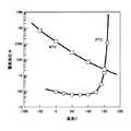
なお、図2に負の温度係数を持つNTCサーミスタと、正の温度係数を持つPTC(Positive Temperature Coefficient)サーミスタそれぞれの温度・抵抗特性を示す。 FIG. 2 shows temperature and resistance characteristics of an NTC thermistor having a negative temperature coefficient and a PTC (Positive Temperature Coefficient) thermistor having a positive temperature coefficient.
保護IC15は、過充電検出回路16、過放電検出回路17、過電流検出回路18を内蔵している。また、保護IC15はリチウムイオン電池12の正極から抵抗R11を通して電源Vddを端子15aに供給されると共に、リチウムイオン電池12の負極から電源Vssを端子15cに供給されて動作する。 The
過充電検出回路16は端子15a、15cの電圧からリチウムイオン電池12の過充電を検出して検出信号を論理回路19に供給する。過放電検出回路17は端子15a、15cの電圧からリチウムイオン電池12の過放電を検出して検出信号を論理回路19に供給する。過電流検出回路18は端子15c、15fの電圧から抵抗R12に流れる電流が過大となる過電流を検出して検出信号を論理回路19に供給する。 The
また、保護IC15は端子15bにサーミスタR13と抵抗R14の接続点Aを接続され、端子15fに抵抗R12の一端を接続され抵抗R12の他端は外部端子14に接続されている。また、保護IC15はDOUT出力の端子15dをMOSトランジスタM11のゲートに接続され、COUT出力の端子15eをMOSトランジスタM12のゲートに接続されている。 The
保護IC15において、端子15bはコンパレータ21の非反転入力端子に接続されている。端子15cはツェナーダイオード等の定電圧源20の負極に接続され、定電圧源20の正極はコンパレータ21の反転入力端子に接続されている。 In the
サーミスタR13は図2に負の温度係数を持つNTCサーミスタであるため、温度が上昇するにしたがって抵抗値が低下して接続点Aの電圧は上昇する。 Since the thermistor R13 is an NTC thermistor having a negative temperature coefficient in FIG. 2, the resistance value decreases and the voltage at the connection point A increases as the temperature increases.
コンパレータ21はヒステリシス特性を有し、定電圧源20で発生した定電圧V1と接続点Aの電圧を比較して、接続点Aの電圧が高いときハイレベルの信号を出力する。つまり、サーミスタR13の検出温度が定電圧V1に対応する所定温度(例えば45°C程度)を超えるとコンパレータ21はハイレベルの高温検出信号を出力する。 The
コンパレータ21の出力する高温検出信号は不感応時間設定回路22に供給される。不感応時間設定回路22は高温検出信号のハイレベル期間が所定値(例えば0.5sec)を超えるとハイレベルの高温検出信号を論理回路19に供給する。 The high temperature detection signal output from the
論理回路19は、過充電検出回路16、過放電検出回路17、過電流検出回路18それぞれの検出信号が供給されると共に、不感応時間設定回路22の出力する高温検出信号が供給されている。 The
論理回路19は過充電検出回路16から過充電検出信号を供給されると端子15eのCOUT出力をローレベルとしてMOSトランジスタM12を遮断し、過放電検出回路17から過放電検出信号を供給されると端子15dのDOUT出力をローレベルとしてMOSトランジスタM11を遮断し、過電流検出回路18から過電流検出信号を供給されると端子15dのDOUT出力をローレベルとしてMOSトランジスタM11を遮断する。 When the overcharge detection signal is supplied from the
論理回路19は高温検出信号がハイレベルとなると、端子15eのCOUT出力をローレベルとしてMOSトランジスタM12を遮断する。これにより、リチウムイオン電池12の温度を正確に検出することができ、リチウムイオン電池12が高温となった場合に充電を停止して保護することができる。 When the high temperature detection signal becomes high level, the
また、サーミスタR13は図2に示すように温度に対してほぼリニアに抵抗値が変化するNTCサーミスタを用いているため温度を精度良く検出でき、サーミスタR13を電池パック10内でリチウムイオン電池12の近傍に配設することによりリチウムイオン電池12の温度を精度良く検出できる。なお、PTCサーミスタはある温度を超えると急激に抵抗値が増加するため温度を精度良く検出できない。 Further, as shown in FIG. 2, the thermistor R13 uses an NTC thermistor whose resistance value changes substantially linearly with respect to the temperature, so that the temperature can be accurately detected. By disposing in the vicinity, the temperature of the
ところで、リチウムイオン電池12は、高温且つ満充電となった場合に破損しやすくなるという特性を有する。このため電池パック10において、リチウムイオン電池12の温度保護を行いつつ、高温時に満充電とならないように充電制御を行うことが好ましい。そこでリチウムイオン電池12の温度保護を高精度に行い、かつ適切な充電制御を行わせるのが以下に説明する本発明の実施形態である。
(第一の実施形態)
図3は、本発明の第一の実施形態の電池パックのブロック図である。同図中、図1と同一部分には同一符号を付す。By the way, the
(First embodiment)
FIG. 3 is a block diagram of the battery pack according to the first embodiment of the present invention. In the figure, the same parts as those in FIG.
本実施形態では、リチウムイオン電池12が所定の温度より高くなったとき、過充電検出回路16Aにおいて過充電を検出する相対的な閾値電圧を低くし、満充電となる前に過充電を検出させる。 In the present embodiment, when the
以下に本実施形態の電池パック10Aについて説明する。 The
本実施形態の電池パック10Aでは、リチウムイオン電池12と並列に抵抗R11とコンデンサC11の直列回路が接続されている。リチウムイオン電池12の正極は配線により電池パック10の外部端子13に接続され、負極は配線により電流遮断用のnチャネルMOSトランジスタM11、M12を介して電池パック10Aの外部端子14に接続されている。 In the
MOSトランジスタM11、M12はドレインを共通接続され、MOSトランジスタM11のソースはリチウムイオン電池12の負極に接続され、MOSトランジスタM12のソースは外部端子14に接続されている。また、MOSトランジスタM11、M12それぞれは、ドレイン・ソース間に等価的にボディダイオードD11、D12が接続されている。 The drains of the MOS transistors M11 and M12 are connected in common, the source of the MOS transistor M11 is connected to the negative electrode of the
また、リチウムイオン電池12と並列にサーミスタR13と抵抗R14の直列回路が接続されている。上記のサーミスタR13は、電池パック10A内でリチウムイオン電池12の近傍に配設されてリチウムイオン電池12と熱結合されている。サーミスタR13は負の温度係数を持つNTC(Negative Temperature Coefficient)サーミスタを用いる。 A series circuit of a thermistor R13 and a resistor R14 is connected in parallel with the
なお、図2に、負の温度係数を持つNTCサーミスタと、正の温度係数を持つPTC(Positive Temperature Coefficient)サーミスタそれぞれの温度・抵抗特性を示す。 FIG. 2 shows temperature and resistance characteristics of an NTC thermistor having a negative temperature coefficient and a PTC (Positive Temperature Coefficient) thermistor having a positive temperature coefficient.
保護IC15Aは、過充電検出回路16A、過放電検出回路17、過電流検出回路18を内蔵している。また、保護IC15Aはリチウムイオン電池12の正極から抵抗R11を通して電源Vddを端子15aに供給されると共に、リチウムイオン電池12の負極から電源Vssを端子15cに供給されて動作する。 The
過充電検出回路16Aは端子15a、15cの電圧からリチウムイオン電池12の過充電を検出して検出信号を論理回路19に供給する。また過充電検出回路16Aには、後述する不感応時間設定回路22から出力される高温検出信号が入力される。過充電検出回路16Aの詳細は後述する。 The
過放電検出回路17は端子15a、15cの電圧からリチウムイオン電池12の過放電を検出して検出信号を論理回路19に供給する。過電流検出回路18は端子15c、15fの電圧から抵抗R12に流れる電流が過大となる過電流を検出して検出信号を論理回路19に供給する。 The
また保護IC15Aは、端子15bにサーミスタR13と抵抗R14の接続点Aを接続され、端子15fに抵抗R12の一端を接続され抵抗R12の他端は外部端子14に接続されている。また、保護IC15AはDOUT出力の端子15dをMOSトランジスタM11のゲートに接続され、COUT出力の端子15eをMOSトランジスタM12のゲートに接続されている。 In the
保護IC15Aにおいて、端子15bはコンパレータ21の非反転入力端子に接続されている。端子15cはツェナーダイオード等の定電圧源20の負極に接続され、定電圧源20の正極はコンパレータ21の反転入力端子に接続されている。 In the
サーミスタR13は図2に示すような負の温度係数を持つNTCサーミスタであるため、温度が上昇するにしたがって抵抗値が低下して接続点Aの電圧は上昇する。 Since the thermistor R13 is an NTC thermistor having a negative temperature coefficient as shown in FIG. 2, the resistance value decreases and the voltage at the connection point A increases as the temperature increases.
コンパレータ21はヒステリシス特性を有し、定電圧源20で発生した定電圧V1と接続点Aの電圧を比較して、接続点Aの電圧が高いときハイレベルの信号を出力する。つまり、サーミスタR13の検出温度が定電圧V1に対応する所定温度(例えば45°C程度)を超えるとコンパレータ21はハイレベルの高温検出信号を出力する。 The
コンパレータ21の出力する高温検出信号は不感応時間設定回路22に供給される。不感応時間設定回路22は高温検出信号のハイレベル期間が所定値(例えば0.5sec)を超えるとハイレベルの高温検出信号を論理回路19に供給する。 The high temperature detection signal output from the
論理回路19は、過充電検出回路16A、過放電検出回路17、過電流検出回路18それぞれの検出信号が供給されると共に、不感応時間設定回路22の出力する高温検出信号が供給されている。 The
論理回路19は過充電検出回路16Aから過充電検出信号を供給されると端子15eのCOUT出力をローレベルとしてMOSトランジスタM12を遮断し、過放電検出回路17から過放電検出信号を供給されると端子15dのDOUT出力をローレベルとしてMOSトランジスタM11を遮断し、過電流検出回路18から過電流検出信号を供給されると端子15dのDOUT出力をローレベルとしてMOSトランジスタM11を遮断する。 When the overcharge detection signal is supplied from the
論理回路19は高温検出信号がハイレベルとなると、端子15eのCOUT出力をローレベルとしてMOSトランジスタM12を遮断する。これにより、リチウムイオン電池12の温度を正確に検出することができ、リチウムイオン電池12が高温となった場合に充電を停止して保護することができる。 When the high temperature detection signal becomes high level, the
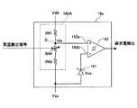
ここで本実施形態の過充電検出回路16Aについてより詳細に説明する。図4は、第一の実施形態の過充電検出回路を説明する図である。 Here, the
過充電検出回路16Aは、分圧回路160、定電圧源161、コンパレータ162、MOSトランジスタM13を有する。 The
分圧回路160は、抵抗R41、R42、R43が直列に接続されて構成されており、電源Vdd及び電源Vss間電圧を分圧する。抵抗R41の一端は端子15aに接続されて電源Vddが供給されており、抵抗R43の一端は端子15cに接続されて電源Vssが供給されている。 The
MOSトランジスタM13は、分圧回路160の分圧比を切り替える切り替え手段である。MOSトランジスタM13のソースが抵抗R41と抵抗R42との接続点Bに接続されており、ドレインが抵抗R42と抵抗R43との接続点Cに接続されている。そしてMOSトランジスタM13のゲートに、不感応時間設定回路22からの出力される高温検出信号が供給される。尚本実施形態のMOSトランジスタM13は、MOSトランジスタM11、MOSトランジスタM12と同様にnチャネルMOSトランジスタとした。 The MOS transistor M13 is a switching unit that switches the voltage dividing ratio of the
定電圧源161は、ツェナーダイオード等の定電圧源であり、定電圧Vocを発生させる。コンパレータ162では、非反転入力端子162aが接続点Bに接続されており、反転入力端子162bが定電圧源161の正極に接続されている。コンパレータ162の出力信号は、論理回路19へ供給される。 The
次に、過充電検出回路16Aの動作について説明する。 Next, the operation of the
過充電検出回路16Aでは、高温検出信号が出力されていない場合、MOSトランジスタM13のゲートにはローレベルの信号が印加され、MOSトランジスタM13はオフの状態となっている。この場合コンパレータ162は、接続点Bの電圧Vinと定電圧源161の電圧とを比較する。電圧Vinは、電源Vdd及び電源Vss間電圧を抵抗R41と抵抗R42及びR43により分圧した電圧である。コンパレータ162は、電圧Vinが定電圧Vocを超えたとき、過充電を検出したことを示すハイレベルの過充電検出信号を出力する。この過充電検出信号は論理回路19へ供給される。論理回路19は、過充電検出信号を検知すると端子15eのCOUT出力をローレベルとしてMOSトランジスタM12を遮断し、充電を停止させる。したがってMOSトランジスタM13がオフの場合には、電源Vdd及び電源Vss間電圧の抵抗R41と抵抗R42及びR43による分圧が、過充電を検出するための相対的な閾値電圧(第一の値)となる。このとき電源Vdd及び電源Vss間電圧の分圧比は、(R42+R43)/(R41+R42+R43)(第一の分圧比)である。 In the
ここでサーミスタR13の検出温度が所定温度以上となり、不感応時間設定回路22から高温検出信号が出力される。MOSトランジスタM13は、高温検出信号がゲートに印加されてオンになり、接続点Bと接続Cとが短絡する。したがってMOSトランジスタM13がオンの場合の接続点Bの電圧Vinは、電源Vdd及び電源Vss間電圧の抵抗R41と抵抗R43による分圧となる。 Here, the detected temperature of the thermistor R13 becomes equal to or higher than a predetermined temperature, and a high temperature detection signal is output from the insensitive
コンパレータ162は、電圧Vinと定電圧Vocとを比較し、電圧Vinが定電圧Vocを超えたとき、過充電を検出したことを示すハイレベルの過充電検出信号を出力する。したがってMOSトランジスタM13がオンの場合には、電源Vdd及び電源Vss間電圧の抵抗R41と抵抗R43による分圧が、過充電を検出するための相対的な閾値電圧(第二の値)となる。このとき電源Vdd及び電源Vss間電圧の分圧比は、R41/(R41+R43)(第二の分圧比)である。尚本実施形態では、第二の分圧比が第一の分圧比よりも小さくなるように各抵抗値を設定することが好ましい。 The
尚本実施形態では、サーミスタR13の検出温度が例えば45°C以上のとき、高温検出信号が出力されるものとした。また本実施形態では、MOSトランジスタM13がオフの状態において、電圧Vinが例えば4.3V(第一の値)になったとき過充電を検出する。そしてMOSトランジスタM13がオンの状態において、電圧Vinが例えば4.1V(第二の値)となったとき過充電を検出するものとした。 In the present embodiment, a high temperature detection signal is output when the detection temperature of the thermistor R13 is 45 ° C. or more, for example. In the present embodiment, overcharge is detected when the voltage Vin becomes, for example, 4.3 V (first value) while the MOS transistor M13 is off. In the state where the MOS transistor M13 is on, overcharge is detected when the voltage Vin becomes 4.1 V (second value), for example.
以下に図5を参照して、本実施形態における相対的な閾値電圧の切り替えについて具体的に説明する。図5は、第一の実施形態のコンパレータ162の動作を説明する図である。図5では、電源Vddを横軸、コンパレータ162の入力端子電圧を縦軸とした。 The relative threshold voltage switching in the present embodiment will be specifically described below with reference to FIG. FIG. 5 is a diagram illustrating the operation of the
本実施形態では、サーミスタR13の検出温度が45°C未満(MOSトランジスタM13がオフ)においてリチウムイオン電池12の充電が開始されると、電圧Vinは、図5のVin1に示すような傾斜となる。この場合コンパレータ162の出力は、電圧Vinが定電圧Vocを超える4.3V(第一の値)になったとき、ハイレベルの過充電検出信号を出力する。 In the present embodiment, when charging of the
また実施形態では、サーミスタR13の検出温度が45°C以上になると、MOSトランジスタM13がオンとなり、電源Vdd及び電源Vss間電圧の分圧比が切り替わる。この状態でリチウムイオン電池12の充電が開始されると、電圧Vinは、図5のVin2に示すような傾斜となる。この場合コンパレータ162は、電圧Vinが定電圧Vocを超える4.1V(第二の値)になったとき、ハイレベルの過充電検出信号を出力する。 In the embodiment, when the detected temperature of the thermistor R13 becomes 45 ° C. or higher, the MOS transistor M13 is turned on, and the voltage division ratio between the power supply Vdd and the power supply Vss is switched. When charging of the
このように本実施形態によれば、サーミスタR13の検出温度に基づきMOSトランジスタM13のオン/オフを制御して、電源Vdd及び電源Vss間の分圧比を切り替えることにより、過充電を検出する相対的な閾値電圧を切り替える。より具体的には本実施形態では、サーミスタR13の検出温度が所定温度以上となったとき、電源Vdd及び電源Vss間の分圧比を第一の分圧比から第二の分圧比に切り替えることで、過充電を検出する相対的な閾値電圧を、第一の分圧比に対応した第一の値から第二の分圧比に対応した第二の値に切り替える。ここで第二の値は第一の値よりも低い値となる。 As described above, according to the present embodiment, the on / off of the MOS transistor M13 is controlled based on the detected temperature of the thermistor R13, and the voltage division ratio between the power supply Vdd and the power supply Vss is switched, thereby detecting the relative overcharge. Switch the threshold voltage. More specifically, in this embodiment, when the detected temperature of the thermistor R13 becomes equal to or higher than a predetermined temperature, the voltage dividing ratio between the power supply Vdd and the power supply Vss is switched from the first voltage dividing ratio to the second voltage dividing ratio. The relative threshold voltage for detecting overcharge is switched from the first value corresponding to the first voltage dividing ratio to the second value corresponding to the second voltage dividing ratio. Here, the second value is lower than the first value.
よって本実施形態では、高温時においてリチウムイオン電池12が満充電となる前に過充電を検出し、充電を停止させることができ、リチウムイオン電池12が高温で且つ満充電となることを防止することができる。したがって本実施形態によれば、リチウムイオン電池12の温度保護を高精度に行い、かつ適切な充電制御を行わせることができる。 Therefore, in this embodiment, overcharge can be detected before the
図6及び図7に本実施形態の過充電検出回路16Aの変形例を示す。図6は、第一の実施形態の過充電検出回路の一変形例を示す図である。図7は、第一の実施形態の過充電検出回路の別の変形例を示す図である。 6 and 7 show a modification of the
図6に示す過充電検出回路16aでは、分圧回路160Aが、抵抗R41、抵抗R43、可変抵抗R44により構成されている。分圧回路160Aでは、電源Vdd及び電源Vss間に抵抗R41、可変抵抗R44、抵抗R43が直列に接続されており、電源Vdd及び電源Vss間電圧を分圧している。本変形例では、可変抵抗R44が分圧回路160Aの分圧比を切り替える切り替え手段となる。抵抗R41と可変抵抗R44との接続点Dは、コンパレータ162の非反転入力と接続されている。分圧回路160Aでは、高温検出信号が出力されると、可変抵抗R44の抵抗値を低下させて電圧Vinを低下させる。よって本変形例では、高温検出信号が出力されたとき、電源Vdd及び電源Vss間の分圧比の切り替えにより、過充電を検出する相対的な閾値電圧を切り替えることができる。 In the
図7に示す過充電検出回路16bでは、分圧回路160Bの分圧比を切り替える切り替え手段として、スイッチ45を有する。分圧回路160Bにおいて、高温検出信号が出力されていない場合、コンパレータ162の非反転入力は、スイッチ45を介して抵抗R41と抵抗R42との接続点Bに接続されている。高温検出信号が出力されと、分圧回路160Bにおいてスイッチ45が切り替わり、コンパレータ162の非反転入力はスイッチ45を介して抵抗R42と抵抗R43との接続点Cに接続される。接続点Cの電圧Vincは、接続点Bの電圧Vinよりも低い電圧である。よって本変形例でも、高温検出信号が出力されたとき、電源Vdd及び電源Vss間の分圧比の切り替えにより、過充電を検出する相対的な閾値電圧を切り替えることができる。
(第二の実施形態)
以下に図面を参照して本発明の第二の実施形態について説明する。第二の実施形態では、サーミスタR13による検出温度が第一の所定温度以上のとき又は第二の所定温度未満のとき、電源Vdd及び電源Vss間の分圧比の切り替えにより過充電を検出する閾値電圧を切り替え、満充電となる前に過充電を検出させる。The
(Second embodiment)
A second embodiment of the present invention will be described below with reference to the drawings. In the second embodiment, when the temperature detected by the thermistor R13 is equal to or higher than the first predetermined temperature or lower than the second predetermined temperature, the threshold voltage for detecting overcharge by switching the voltage division ratio between the power supply Vdd and the power supply Vss. And overcharge is detected before the battery is fully charged.
図8は、本発明の第二の実施形態の電池パックのブロック図である。同図中、第一の実施形態と同一部分には第一の実施形態を説明する図3と同一符号を付し、その説明を省略する。 FIG. 8 is a block diagram of the battery pack according to the second embodiment of the present invention. In the figure, the same parts as those in the first embodiment are denoted by the same reference numerals as those in FIG. 3 for explaining the first embodiment, and the description thereof is omitted.
電池パック10Bの有する保護IC15Bは、サーミスタR13の検出温度が第一の所定温度以上であることを検出するコンパレータ21と、サーミスタR13の検出温度が第二の所定温度未満であることを検出するコンパレータ21Aとを有する。尚本実施形態では、第一の所定温度を例えば45°C程度とし、第二の所定温度を例えば0°C程度とした。 The
コンパレータ21Aの反転入力端子は、端子15bに接続されている。コンパレータ21Aの非反転入力端子はツェナーダイオード等の定電圧源20Aの正極に接続されている。定電圧源20Aの負極は、端子15cに接続されている。コンパレータ21Aは、サーミスタR13の検出温度が定電圧V2に対応する所定温度(例えば0°C程度)未満になるとハイレベルの低温検出信号を出力する。 The inverting input terminal of the
コンパレータ21Aの出力する低温検出信号は不感応時間設定回路22に供給される。不感応時間設定回路22は、低温検出信号のハイレベル期間が所定値(例えば0.5sec)を超えるとハイレベルの低温検出信号を過充電検出回路16Bに供給する。 The low temperature detection signal output from the
図9は、第二の実施形態の過充電検出回路を説明する図である。 FIG. 9 is a diagram illustrating an overcharge detection circuit according to the second embodiment.
本実施形態の過充電検出回路16Bは、第一の実施形態の過充電検出回路16Aと同様の構成であるが、MOSトランジスタM13のゲートに高温検出信号又は低温検出信号の何れか一方が供給される点で第一の実施形態と異なる。 The
本実施形態の過充電検出回路16Bでは、ハイレベルの高温検出信号又はハイレベルの低温検出信号が出力された場合に、第一の実施形態の過充電検出回路16Aと同様の動作を行う。 The
したがって本実施形態によれば、サーミスタR13による検出温度が第一の所定温度以上の場合又は検出温度が第二の所定温度未満の場合に、過充電を検出する相対的な閾値電圧を低くすることができる。このためリチウムイオン電池12が高温又は低温の場合に、リチウムイオン電池12が満充電となることを防止でき、リチウムイオン電池12の温度保護を高精度に行い、かつ適切な充電制御を行わせることができる。 Therefore, according to this embodiment, when the temperature detected by the thermistor R13 is equal to or higher than the first predetermined temperature or when the temperature detected is lower than the second predetermined temperature, the relative threshold voltage for detecting overcharge is lowered. Can do. Therefore, when the
以上、各実施形態に基づき本発明の説明を行ってきたが、上記実施形態に示した要件に本発明が限定されるものではない。これらの点に関しては、本発明の主旨をそこなわない範囲で変更することができ、その応用形態に応じて適切に定めることができる。 As mentioned above, although this invention has been demonstrated based on each embodiment, this invention is not limited to the requirements shown in the said embodiment. With respect to these points, the gist of the present invention can be changed without departing from the scope of the present invention, and can be appropriately determined according to the application form.
10、10A、10B 電池パック
12 リチウムイオン電池
13、14 外部端子
15、15A、15B 保護IC
16、16A、16B 過充電検出回路
17 過放電検出回路
18 過電流検出回路
19 論理回路
20 定電圧源
21、21A、162 コンパレータ
22 不感応時間設定回路
M11、M12、M13 MOSトランジスタ
R11、R12、R41、R42、R41 抵抗
R13 サーミスタ
R44 可変抵抗
160、160A、160B 分圧回路10, 10A,
16, 16A, 16B
Claims (4)
Translated fromJapanese前記二次電池の近傍に配設され前記二次電池と並列接続されたサーミスと抵抗の直列回路と、
前記サーミスタと抵抗の接続点の電圧を第一の所定温度に対応する第一の基準電圧と比較する第一のコンパレータと、
前記第一のコンパレータの出力にしたがって、前記二次電池の温度が前記第一の所定温度未満のとき前記閾値電圧を第一の値とし、前記二次電池の温度が前記第一の所定温度以上のとき前記閾値電圧を前記第一の値よりも低い第二の値とする切り替え手段と、
を有することを特徴とする電池パック。An overcharge detection circuit detects the overcharge of the secondary battery by comparing the voltage between the positive electrode and the negative electrode of the secondary battery with a threshold voltage, and is provided in the wiring between the secondary battery and the load or charging device. In the battery pack that turns off the switch element,
A thermist and resistor series circuit arranged in the vicinity of the secondary battery and connected in parallel with the secondary battery;
A first comparator for comparing a voltage at a connection point between the thermistor and the resistor with a first reference voltage corresponding to a first predetermined temperature;
According to the output of the first comparator, when the temperature of the secondary battery is lower than the first predetermined temperature, the threshold voltage is set to a first value, and the temperature of the secondary battery is equal to or higher than the first predetermined temperature. Switching means for setting the threshold voltage to a second value lower than the first value,
A battery pack comprising:
前記二次電池の正極及び負極間の電圧を分圧する分圧回路と、前記分圧回路で分圧した電圧を一定の閾値電圧と比較する第二のコンパレータとを有し、
前記切り替え手段は、前記第一のコンパレータの出力にしたがって、前記二次電池の温度が前記第一の所定温度未満のとき前記分圧回路を第一の分圧比とし、前記二次電池の温度が前記第一の所定温度以上のとき前記分圧回路を前記第一の分圧比よりも小さい第二の分圧比として、相対的に前記閾値電圧を切り替えることを特徴とする請求項1記載の電池パック。The overcharge detection circuit is
A voltage dividing circuit for dividing the voltage between the positive electrode and the negative electrode of the secondary battery, and a second comparator for comparing the voltage divided by the voltage dividing circuit with a certain threshold voltage,
According to the output of the first comparator, the switching means sets the voltage dividing circuit to a first voltage dividing ratio when the temperature of the secondary battery is lower than the first predetermined temperature, and the temperature of the secondary battery is 2. The battery pack according to claim 1, wherein when the temperature is equal to or higher than the first predetermined temperature, the threshold voltage is relatively switched by setting the voltage dividing circuit as a second voltage dividing ratio smaller than the first voltage dividing ratio. .
前記第三のコンパレータの出力にしたがって、前記二次電池の温度が前記第二の所定温度未満のとき前記分圧回路を第二の分圧比として、相対的に前記閾値電圧を切り替えることを特徴とする請求項2記載の電池パック。The switching means further includes a third comparator for comparing a voltage at a connection point between the thermistor and the resistor with a second reference voltage corresponding to a second predetermined temperature lower than the first predetermined temperature,
According to the output of the third comparator, when the temperature of the secondary battery is lower than the second predetermined temperature, the threshold voltage is switched relatively by using the voltage dividing circuit as a second voltage dividing ratio. The battery pack according to claim 2.
Priority Applications (6)
| Application Number | Priority Date | Filing Date | Title |
|---|---|---|---|
| JP2007330580AJP5061884B2 (en) | 2007-12-21 | 2007-12-21 | Battery pack |
| US12/334,674US8305041B2 (en) | 2007-12-21 | 2008-12-15 | Battery pack |
| CN201310221707.0ACN103326326B (en) | 2007-12-21 | 2008-12-18 | battery pack and integrated circuit |
| CN2008101860067ACN101465539B (en) | 2007-12-21 | 2008-12-18 | Battery pack |
| JP2012172925AJP2012254016A (en) | 2007-12-21 | 2012-08-03 | Overcharge detection circuit, battery pack and integrated circuit |
| US13/644,643US9438050B2 (en) | 2007-12-21 | 2012-10-04 | Overcharge detecting circuit and integrated circuit |
Applications Claiming Priority (1)
| Application Number | Priority Date | Filing Date | Title |
|---|---|---|---|
| JP2007330580AJP5061884B2 (en) | 2007-12-21 | 2007-12-21 | Battery pack |
Related Child Applications (1)
| Application Number | Title | Priority Date | Filing Date |
|---|---|---|---|
| JP2012172925ADivisionJP2012254016A (en) | 2007-12-21 | 2012-08-03 | Overcharge detection circuit, battery pack and integrated circuit |
Publications (2)
| Publication Number | Publication Date |
|---|---|
| JP2009152129A JP2009152129A (en) | 2009-07-09 |
| JP5061884B2true JP5061884B2 (en) | 2012-10-31 |
Family
ID=40787789
Family Applications (2)
| Application Number | Title | Priority Date | Filing Date |
|---|---|---|---|
| JP2007330580AActiveJP5061884B2 (en) | 2007-12-21 | 2007-12-21 | Battery pack |
| JP2012172925APendingJP2012254016A (en) | 2007-12-21 | 2012-08-03 | Overcharge detection circuit, battery pack and integrated circuit |
Family Applications After (1)
| Application Number | Title | Priority Date | Filing Date |
|---|---|---|---|
| JP2012172925APendingJP2012254016A (en) | 2007-12-21 | 2012-08-03 | Overcharge detection circuit, battery pack and integrated circuit |
Country Status (3)
| Country | Link |
|---|---|
| US (2) | US8305041B2 (en) |
| JP (2) | JP5061884B2 (en) |
| CN (2) | CN103326326B (en) |
Families Citing this family (37)
| Publication number | Priority date | Publication date | Assignee | Title |
|---|---|---|---|---|
| JP5061884B2 (en)* | 2007-12-21 | 2012-10-31 | ミツミ電機株式会社 | Battery pack |
| JP5061935B2 (en)* | 2008-02-12 | 2012-10-31 | ミツミ電機株式会社 | Battery pack |
| JP2010016975A (en)* | 2008-07-03 | 2010-01-21 | Hitachi Koki Co Ltd | Charging system and battery pack used for the system |
| WO2010002040A2 (en)* | 2008-07-03 | 2010-01-07 | Hitachi Koki Co., Ltd. | Charging system and battery pack |
| TWI390818B (en)* | 2009-07-14 | 2013-03-21 | Richpower Microelectronics | Apparatus and method for improving the standby efficiency of a charger, and ultra low standby power charge |
| US8552693B2 (en)* | 2009-07-17 | 2013-10-08 | Tesla Motors, Inc. | Low temperature charging of Li-ion cells |
| JP5428675B2 (en)* | 2009-09-09 | 2014-02-26 | 株式会社リコー | Secondary battery protection circuit, battery pack and electronic equipment |
| JP5462043B2 (en)* | 2010-03-19 | 2014-04-02 | セイコーインスツル株式会社 | Battery state monitoring circuit and battery device |
| JP5462046B2 (en)* | 2010-03-26 | 2014-04-02 | セイコーインスツル株式会社 | Battery state monitoring circuit and battery device |
| JP2012100376A (en)* | 2010-10-29 | 2012-05-24 | Mitsumi Electric Co Ltd | Switching power supply device |
| JP5742524B2 (en) | 2011-07-08 | 2015-07-01 | ソニー株式会社 | Control device, power storage system, electronic device, electric vehicle, and power system |
| JP2013059212A (en)* | 2011-09-08 | 2013-03-28 | Mitsumi Electric Co Ltd | Battery protection circuit, battery protection device and battery pack |
| CN103683203A (en)* | 2012-09-21 | 2014-03-26 | 科域半导体有限公司 | Switching Power Converter Overheating Protection |
| US10739210B2 (en)* | 2012-12-04 | 2020-08-11 | Oxford University Innovation Limited | Sensor, controller and system |
| CN104242253A (en)* | 2014-09-30 | 2014-12-24 | 成都闰世科技有限公司 | Lithium battery protection based on-board PTC (positive temperature coefficient) protection circuit |
| JP5888387B1 (en) | 2014-10-22 | 2016-03-22 | ミツミ電機株式会社 | Battery protection circuit, battery protection device, and battery pack |
| JP6646877B2 (en)* | 2014-12-12 | 2020-02-14 | Dic株式会社 | Polyarylene sulfide resin composition, molded article, composite molded article, and method for producing composite molded article |
| JP6416665B2 (en)* | 2015-03-11 | 2018-10-31 | 株式会社マキタ | Battery connection system and battery pack |
| KR102442187B1 (en)* | 2015-04-10 | 2022-09-07 | 삼성에스디아이 주식회사 | Battery protection circuit |
| JP6736996B2 (en)* | 2016-06-14 | 2020-08-05 | アイシン精機株式会社 | Power shutoff device |
| CN106532835B (en)* | 2016-12-06 | 2019-04-09 | 湖北大学 | Charging devices and chargers |
| US10622836B2 (en)* | 2017-05-02 | 2020-04-14 | Advanced Semiconductor Engineering, Inc. | Power management system and method for operating the same |
| EP3657591B1 (en)* | 2017-08-25 | 2021-07-14 | Guangdong Oppo Mobile Telecommunications Corp., Ltd. | Terminal device and battery safety monitoring method and monitoring system therefor |
| KR102474424B1 (en)* | 2017-10-31 | 2022-12-05 | 주식회사 엘엑스세미콘 | Communication method between master controller and slave controller, the slave controller for the same, and battery management system using the same |
| CN108448679B (en)* | 2018-04-04 | 2020-09-04 | 中国科学院上海高等研究院 | Intelligent battery management unit, battery discharging overcurrent self-recovery system and self-recovery method |
| CN108321909A (en)* | 2018-04-04 | 2018-07-24 | 中国科学院上海高等研究院 | Intelligent battery administrative unit, the over-pressed self recoverable system of battery charging and self-recovery method |
| FR3081265B1 (en)* | 2018-05-17 | 2020-06-12 | Valeo Siemens Eautomotive France Sas | PROTECTION CIRCUIT OF A SWITCH |
| CN109066888B (en)* | 2018-09-05 | 2021-11-30 | 歌尔科技有限公司 | Charging control circuit with temperature protection function and electronic product |
| US11714138B2 (en) | 2018-11-22 | 2023-08-01 | Semiconductor Energy Laboratory Co., Ltd. | Semiconductor device, power storage device, and electronic device |
| CN113196659A (en) | 2018-12-19 | 2021-07-30 | 株式会社半导体能源研究所 | Hysteresis comparator, semiconductor device, and power storage device |
| CN109713750A (en)* | 2018-12-30 | 2019-05-03 | 深圳飞安瑞科技股份有限公司 | A kind of adjustable charge-discharge battery protection circuit of temperature |
| JP6608082B1 (en)* | 2019-01-17 | 2019-11-20 | 日本たばこ産業株式会社 | Power supply unit for aerosol inhaler |
| JP6614388B1 (en)* | 2019-05-31 | 2019-12-04 | ミツミ電機株式会社 | Secondary battery protection circuit, secondary battery protection device, battery pack, and control method of secondary battery protection circuit |
| CN113892221A (en)* | 2019-06-27 | 2022-01-04 | 三洋电机株式会社 | Battery pack and abnormality monitoring method thereof |
| KR102864758B1 (en)* | 2020-07-17 | 2025-09-24 | 주식회사 엘지에너지솔루션 | Apparatus for managing battery |
| CN112737055B (en)* | 2021-01-13 | 2022-11-01 | 南昌嘉信高科技有限公司 | Charging protection circuit and electronic equipment |
| DE112022000290T5 (en)* | 2021-01-20 | 2023-09-14 | Rohm Co., Ltd. | SELF-DIAGNOSIS CIRCUIT AND SEMICONDUCTOR COMPONENT |
Family Cites Families (25)
| Publication number | Priority date | Publication date | Assignee | Title |
|---|---|---|---|---|
| US4618857A (en)* | 1984-06-20 | 1986-10-21 | Harvey W. Dubois | Low D.C. and loss of A.C. sensor and alarm with service inhibitor |
| US4616216A (en)* | 1984-07-27 | 1986-10-07 | Earl Joseph Schnur | Emergency stop monitor |
| US5136231A (en)* | 1990-10-12 | 1992-08-04 | Compaq Computer Corporation | Ni-cad battery charge rate controller |
| US5703468A (en)* | 1995-03-17 | 1997-12-30 | Petrillo; Gino A. | Electrical charge control apparatus and method for photovoltaic energy conversion systems |
| JP3305257B2 (en)* | 1998-05-06 | 2002-07-22 | セイコーインスツルメンツ株式会社 | Charge / discharge control circuit, rechargeable power supply device and control method therefor |
| JP2001061232A (en)* | 1999-08-20 | 2001-03-06 | Toshiba Electronic Engineering Corp | Secondary battery protection circuit device |
| US6340880B1 (en)* | 1999-11-11 | 2002-01-22 | Mitsumi Electric Co., Ltd. | Method of protecting a chargeable electric cell |
| JP4127944B2 (en) | 2000-01-14 | 2008-07-30 | 九州日立マクセル株式会社 | Rechargeable small electrical equipment |
| JP4051182B2 (en) | 2001-04-17 | 2008-02-20 | 矢崎総業株式会社 | Overcurrent detection device |
| JP2003037944A (en)* | 2001-07-25 | 2003-02-07 | Seiko Instruments Inc | Charging/discharging control circuit and rechargeable power supply |
| JP4057260B2 (en) | 2001-08-07 | 2008-03-05 | 株式会社日立製作所 | Power supply circuit, power supply system, and electronic device |
| JP2003173825A (en)* | 2001-09-28 | 2003-06-20 | Mitsumi Electric Co Ltd | Secondary battery protector |
| JP4329326B2 (en)* | 2002-10-30 | 2009-09-09 | パナソニック株式会社 | Secondary battery and secondary battery pack with temperature protection element unit |
| US6819083B1 (en)* | 2003-04-25 | 2004-11-16 | Motorola, Inc. | Dual use thermistor for battery cell thermal protection and battery pack overcharge/undercharge protection |
| JP4079871B2 (en) | 2003-12-17 | 2008-04-23 | 三洋電機株式会社 | Pack battery |
| JP4767566B2 (en)* | 2004-04-22 | 2011-09-07 | パナソニック株式会社 | Lithium secondary battery charger and electronic device including the charger |
| US7248023B2 (en)* | 2004-04-22 | 2007-07-24 | Matsushita Electric Industrial Co., Ltd. | Charger for lithium secondary battery and electronic apparatus including charger |
| JP4788398B2 (en)* | 2006-02-27 | 2011-10-05 | パナソニック電工株式会社 | Charger |
| JP2009005559A (en)* | 2007-06-25 | 2009-01-08 | Mitsumi Electric Co Ltd | Battery pack |
| JP2009005558A (en)* | 2007-06-25 | 2009-01-08 | Mitsumi Electric Co Ltd | Battery pack |
| JP5338047B2 (en)* | 2007-08-07 | 2013-11-13 | ミツミ電機株式会社 | Battery pack |
| JP5098501B2 (en)* | 2007-08-07 | 2012-12-12 | ミツミ電機株式会社 | Battery pack |
| JP2009055755A (en)* | 2007-08-29 | 2009-03-12 | Ricoh Co Ltd | Secondary battery protection semiconductor device |
| JP4953249B2 (en)* | 2007-11-22 | 2012-06-13 | ソニーモバイルコミュニケーションズ株式会社 | Portable device |
| JP5061884B2 (en)* | 2007-12-21 | 2012-10-31 | ミツミ電機株式会社 | Battery pack |
- 2007
- 2007-12-21JPJP2007330580Apatent/JP5061884B2/enactiveActive
- 2008
- 2008-12-15USUS12/334,674patent/US8305041B2/enactiveActive
- 2008-12-18CNCN201310221707.0Apatent/CN103326326B/enactiveActive
- 2008-12-18CNCN2008101860067Apatent/CN101465539B/enactiveActive
- 2012
- 2012-08-03JPJP2012172925Apatent/JP2012254016A/enactivePending
- 2012-10-04USUS13/644,643patent/US9438050B2/enactiveActive
Also Published As
| Publication number | Publication date |
|---|---|
| CN101465539A (en) | 2009-06-24 |
| US9438050B2 (en) | 2016-09-06 |
| CN103326326A (en) | 2013-09-25 |
| JP2012254016A (en) | 2012-12-20 |
| JP2009152129A (en) | 2009-07-09 |
| US8305041B2 (en) | 2012-11-06 |
| CN103326326B (en) | 2016-05-04 |
| CN101465539B (en) | 2013-10-09 |
| US20090160405A1 (en) | 2009-06-25 |
| US20130026997A1 (en) | 2013-01-31 |
Similar Documents
| Publication | Publication Date | Title |
|---|---|---|
| JP5061884B2 (en) | Battery pack | |
| JP5061935B2 (en) | Battery pack | |
| JP7538452B2 (en) | Secondary battery protection device, battery pack, and method for controlling secondary battery protection device | |
| US8148946B2 (en) | Battery pack having protection circuit for secondary battery | |
| US8193774B2 (en) | Battery pack | |
| JP5439800B2 (en) | Secondary battery protection integrated circuit device, secondary battery protection module using the same, and battery pack | |
| JP2009005558A (en) | Battery pack | |
| JP4761454B2 (en) | Charge / discharge protection circuit and power supply device | |
| US8524385B2 (en) | Battery pack | |
| JP5098501B2 (en) | Battery pack | |
| JP5588370B2 (en) | Output circuit, temperature switch IC, and battery pack | |
| JP5338047B2 (en) | Battery pack | |
| JP2014064459A (en) | Protection circuit and battery pack | |
| JP2006320048A (en) | Protection circuit | |
| CN101728841A (en) | Battery case | |
| JP2006121827A (en) | Protection circuit for secondary battery | |
| JP2009183050A (en) | Battery pack | |
| CN101728842A (en) | Battery case | |
| KR101027104B1 (en) | Battery pack | |
| KR101085725B1 (en) | Battery pack | |
| JP2017189430A (en) | Charge/discharge protection system and charging type vacuum cleaner | |
| JP2010279083A (en) | Protection circuit |
Legal Events
| Date | Code | Title | Description |
|---|---|---|---|
| A621 | Written request for application examination | Free format text:JAPANESE INTERMEDIATE CODE: A621 Effective date:20101126 | |
| TRDD | Decision of grant or rejection written | ||
| A01 | Written decision to grant a patent or to grant a registration (utility model) | Free format text:JAPANESE INTERMEDIATE CODE: A01 Effective date:20120710 | |
| A01 | Written decision to grant a patent or to grant a registration (utility model) | Free format text:JAPANESE INTERMEDIATE CODE: A01 | |
| A61 | First payment of annual fees (during grant procedure) | Free format text:JAPANESE INTERMEDIATE CODE: A61 Effective date:20120723 | |
| R150 | Certificate of patent or registration of utility model | Ref document number:5061884 Country of ref document:JP Free format text:JAPANESE INTERMEDIATE CODE: R150 Free format text:JAPANESE INTERMEDIATE CODE: R150 | |
| FPAY | Renewal fee payment (event date is renewal date of database) | Free format text:PAYMENT UNTIL: 20150817 Year of fee payment:3 |