JP5060738B2 - Image display device - Google Patents
Image display deviceDownload PDFInfo
- Publication number
- JP5060738B2 JP5060738B2JP2006125338AJP2006125338AJP5060738B2JP 5060738 B2JP5060738 B2JP 5060738B2JP 2006125338 AJP2006125338 AJP 2006125338AJP 2006125338 AJP2006125338 AJP 2006125338AJP 5060738 B2JP5060738 B2JP 5060738B2
- Authority
- JP
- Japan
- Prior art keywords
- electrode
- image display
- gate
- display device
- layer
- Prior art date
- Legal status (The legal status is an assumption and is not a legal conclusion. Google has not performed a legal analysis and makes no representation as to the accuracy of the status listed.)
- Active
Links
Images


Classifications
- H—ELECTRICITY
- H10—SEMICONDUCTOR DEVICES; ELECTRIC SOLID-STATE DEVICES NOT OTHERWISE PROVIDED FOR
- H10D—INORGANIC ELECTRIC SEMICONDUCTOR DEVICES
- H10D86/00—Integrated devices formed in or on insulating or conducting substrates, e.g. formed in silicon-on-insulator [SOI] substrates or on stainless steel or glass substrates
- H10D86/01—Manufacture or treatment
- H10D86/021—Manufacture or treatment of multiple TFTs
- H10D86/0231—Manufacture or treatment of multiple TFTs using masks, e.g. half-tone masks
- H—ELECTRICITY
- H10—SEMICONDUCTOR DEVICES; ELECTRIC SOLID-STATE DEVICES NOT OTHERWISE PROVIDED FOR
- H10D—INORGANIC ELECTRIC SEMICONDUCTOR DEVICES
- H10D30/00—Field-effect transistors [FET]
- H10D30/60—Insulated-gate field-effect transistors [IGFET]
- H10D30/67—Thin-film transistors [TFT]
- H10D30/6729—Thin-film transistors [TFT] characterised by the electrodes
- H10D30/6737—Thin-film transistors [TFT] characterised by the electrodes characterised by the electrode materials
- H10D30/6739—Conductor-insulator-semiconductor electrodes
- H—ELECTRICITY
- H10—SEMICONDUCTOR DEVICES; ELECTRIC SOLID-STATE DEVICES NOT OTHERWISE PROVIDED FOR
- H10D—INORGANIC ELECTRIC SEMICONDUCTOR DEVICES
- H10D86/00—Integrated devices formed in or on insulating or conducting substrates, e.g. formed in silicon-on-insulator [SOI] substrates or on stainless steel or glass substrates
- H10D86/40—Integrated devices formed in or on insulating or conducting substrates, e.g. formed in silicon-on-insulator [SOI] substrates or on stainless steel or glass substrates characterised by multiple TFTs
- H10D86/441—Interconnections, e.g. scanning lines
- H—ELECTRICITY
- H10—SEMICONDUCTOR DEVICES; ELECTRIC SOLID-STATE DEVICES NOT OTHERWISE PROVIDED FOR
- H10D—INORGANIC ELECTRIC SEMICONDUCTOR DEVICES
- H10D86/00—Integrated devices formed in or on insulating or conducting substrates, e.g. formed in silicon-on-insulator [SOI] substrates or on stainless steel or glass substrates
- H10D86/40—Integrated devices formed in or on insulating or conducting substrates, e.g. formed in silicon-on-insulator [SOI] substrates or on stainless steel or glass substrates characterised by multiple TFTs
- H10D86/481—Integrated devices formed in or on insulating or conducting substrates, e.g. formed in silicon-on-insulator [SOI] substrates or on stainless steel or glass substrates characterised by multiple TFTs integrated with passive devices, e.g. auxiliary capacitors
- H—ELECTRICITY
- H10—SEMICONDUCTOR DEVICES; ELECTRIC SOLID-STATE DEVICES NOT OTHERWISE PROVIDED FOR
- H10D—INORGANIC ELECTRIC SEMICONDUCTOR DEVICES
- H10D86/00—Integrated devices formed in or on insulating or conducting substrates, e.g. formed in silicon-on-insulator [SOI] substrates or on stainless steel or glass substrates
- H10D86/40—Integrated devices formed in or on insulating or conducting substrates, e.g. formed in silicon-on-insulator [SOI] substrates or on stainless steel or glass substrates characterised by multiple TFTs
- H10D86/60—Integrated devices formed in or on insulating or conducting substrates, e.g. formed in silicon-on-insulator [SOI] substrates or on stainless steel or glass substrates characterised by multiple TFTs wherein the TFTs are in active matrices
- H—ELECTRICITY
- H10—SEMICONDUCTOR DEVICES; ELECTRIC SOLID-STATE DEVICES NOT OTHERWISE PROVIDED FOR
- H10K—ORGANIC ELECTRIC SOLID-STATE DEVICES
- H10K59/00—Integrated devices, or assemblies of multiple devices, comprising at least one organic light-emitting element covered by group H10K50/00
- H10K59/10—OLED displays
- H10K59/12—Active-matrix OLED [AMOLED] displays
- H10K59/1201—Manufacture or treatment
- H—ELECTRICITY
- H10—SEMICONDUCTOR DEVICES; ELECTRIC SOLID-STATE DEVICES NOT OTHERWISE PROVIDED FOR
- H10K—ORGANIC ELECTRIC SOLID-STATE DEVICES
- H10K59/00—Integrated devices, or assemblies of multiple devices, comprising at least one organic light-emitting element covered by group H10K50/00
- H10K59/10—OLED displays
- H10K59/12—Active-matrix OLED [AMOLED] displays
- H10K59/121—Active-matrix OLED [AMOLED] displays characterised by the geometry or disposition of pixel elements
- H—ELECTRICITY
- H10—SEMICONDUCTOR DEVICES; ELECTRIC SOLID-STATE DEVICES NOT OTHERWISE PROVIDED FOR
- H10K—ORGANIC ELECTRIC SOLID-STATE DEVICES
- H10K59/00—Integrated devices, or assemblies of multiple devices, comprising at least one organic light-emitting element covered by group H10K50/00
- H10K59/10—OLED displays
- H10K59/12—Active-matrix OLED [AMOLED] displays
- H10K59/131—Interconnections, e.g. wiring lines or terminals
Landscapes
- Engineering & Computer Science (AREA)
- Microelectronics & Electronic Packaging (AREA)
- Physics & Mathematics (AREA)
- Geometry (AREA)
- Manufacturing & Machinery (AREA)
- Thin Film Transistor (AREA)
- Liquid Crystal (AREA)
- Devices For Indicating Variable Information By Combining Individual Elements (AREA)
Description
Translated fromJapanese 本発明は、画像表示装置に係り、特に低コストで製造可能な画像表示装置に関する。
The present invention relates to an image display device, and more particularly toan image display device thatcan be manufactured at low cost.
ポリシリコン薄膜トランジスタ(TFTと記す)は、アモルファスシリコンTFTよりも移動度が2桁以上高い優れた性能を有する。この特長を活かした例として、例えば非特許文献1に記載されているアクティブマトリクス型液晶表示装置を挙げることができる。この画像表示装置は、フラットパネルディスプレイ(FPD)と称する平板型の画像表示装置である。この表示装置の周辺駆動回路の一部をポリシリコンTFTで構成することにより、画素部と周辺駆動回路との接続端子数を低減することができ、高精細な画像表示が実現可能である。 Polysilicon thin film transistors (referred to as TFTs) have superior performance that is two orders of magnitude higher than amorphous silicon TFTs. As an example utilizing this feature, for example, an active matrix liquid crystal display device described in Non-Patent
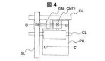
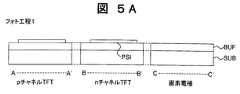
図2は、従来の画像表示装置の回路構成図である。また、この液晶表示装置の周辺駆動回路1を構成するCMOS薄膜トランジスタ(MOS)2の平面図および画素3の平面図を図3、図4にそれぞれ示す。そして、従来の液晶表示装置の製造方法を図3と図4のA−A’断面、B−B’断面、C−C’断面を用いて図5A〜図5Gに従って説明する。A−A’断面はpチャネルTFTの部分、B−B’断面はnチャネルTFTの部分、C−C’断面は画素電極の部分である。 FIG. 2 is a circuit configuration diagram of a conventional image display apparatus. 3 and 4 are a plan view of a CMOS thin film transistor (MOS) 2 and a plan view of a
絶縁性基板であるガラス基板SUB上にバッファ層として酸化シリコン膜BUFを100nm堆積し、さらにプラズマCVD法によりアモルファスシリコン層を50nm堆積する。次に、XeClエキシマレーザを照射しアモルファスシリコン層を結晶化し、公知のフォトリソグラフィ―エッチング工程(フォト工程1)により、島状のポリシリコン層PSIを得る(図5A)。その後、プラズマCVD法によりゲート絶縁膜OX1を100nm堆積し、nチャネルTFTのしきい値調整のためボロンイオンを打ち込む。さらに、公知のフォトリソグラフィ工程により、nチャネルTFTの領域をレジストで覆い(フォト工程2)、レジストをマスクとして、pチャネルTFTの閾値調整のためリンのイオンを打ち込む(図5B)。 A silicon oxide film BUF is deposited to a thickness of 100 nm as a buffer layer on a glass substrate SUB that is an insulating substrate, and an amorphous silicon layer is deposited to a thickness of 50 nm by plasma CVD. Next, XeCl excimer laser is irradiated to crystallize the amorphous silicon layer, and an island-shaped polysilicon layer PSI is obtained by a known photolithography-etching process (photo process 1) (FIG. 5A). Thereafter, a gate insulating film OX1 is deposited to 100 nm by plasma CVD, and boron ions are implanted to adjust the threshold value of the n-channel TFT. Further, the n-channel TFT region is covered with a resist by a known photolithography process (photo process 2), and phosphorus ions are implanted to adjust the threshold value of the p-channel TFT using the resist as a mask (FIG. 5B).
その後、例えばタングステン(W)からなる金属層を堆積し、公知のフォトリソグラフィ―エッチング工程(フォト工程3)によりゲート電極GMおよびゲート線GL(図4参照)を形成する。次に、ゲート電極をマスクとして、リン(燐)イオン打ち込みによって低濃度n型ポリシリコン層LDNを形成する(図5C)。その後、公知のフォトリソグラフィ工程によりゲート電極および低濃度n型ポリシリコン層LDNの一部をレジストで覆い(フォト工程4)、レジストをマスクとして高濃度n型ポリシリコン層HDNを形成する(図5D)。さらに、公知のフォトリソグラフィ工程により、nチャネルTFTの領域をレジストで覆い(フォト工程5)、レジストをマスクとして、高濃度p型ポリシリコン層HDPを形成する(図5E)。 Thereafter, a metal layer made of, for example, tungsten (W) is deposited, and a gate electrode GM and a gate line GL (see FIG. 4) are formed by a known photolithography-etching process (photo process 3). Next, a low concentration n-type polysilicon layer LDN is formed by phosphorus (phosphorus) ion implantation using the gate electrode as a mask (FIG. 5C). Thereafter, a part of the gate electrode and the low-concentration n-type polysilicon layer LDN is covered with a resist by a known photolithography process (photo process 4), and a high-concentration n-type polysilicon layer HDN is formed using the resist as a mask (FIG. 5D). ). Further, the n-channel TFT region is covered with a resist by a known photolithography process (photo process 5), and a high-concentration p-type polysilicon layer HDP is formed using the resist as a mask (FIG. 5E).
その後、表面全体を覆うようにプラズマCVD法により層間絶縁膜OX2を形成し、公知のフォトフォトリソグラフィ―エッチング工程(フォト工程6)によりコンタクトホールCNT1を形成する。さらに、例えばアルミニウム(Al)からなる金属層を堆積し、公知のフォトフォトリソグラフィ―エッチング工程(フォト工程7)により、ソース/ドレイン電極SDMおよび信号線を形成する(図5F)。 Thereafter, an interlayer insulating film OX2 is formed by plasma CVD so as to cover the entire surface, and a contact hole CNT1 is formed by a known photolithography-etching process (photo process 6). Further, a metal layer made of, for example, aluminum (Al) is deposited, and a source / drain electrode SDM and a signal line are formed by a known photolithography-etching process (photo process 7) (FIG. 5F).
その後、全体を覆うように窒化シリコン(SiN)からなる保護絶縁膜PAS1と有機材料からなる保護絶縁膜PAS2を形成し、公知のフォトフォトリソグラフィ―エッチング工程(フォト工程8)によりコンタクトホールCNT2を形成する。その後、公知のフォトフォトリソグラフィ―エッチング工程(フォト工程9)により、Indium Tin Oxide(ITO)からなる画素電極PXを形成する(図5G)。
従来のポリシリコンTFT製造工程では、同じ絶縁基板上にnチャネルTFTとpチャネルTFTを作り分ける必要があるため、しきい値調整および、高濃度不純物領域を形成するためのイオン打ち込みのためのフォトリソグラフィ工程が増加してしまい、スループットが低下してしまう。 In the conventional polysilicon TFT manufacturing process, it is necessary to separately form an n-channel TFT and a p-channel TFT on the same insulating substrate. Therefore, a photo for ion implantation for adjusting a threshold value and forming a high-concentration impurity region. Lithography steps increase and throughput decreases.
本発明の目的は、ポリシリコンTFT製造工程でのフォトリソグラフィ工程を削減することにより、スループットを向上させて低コストで製造可能な画像表示装置を提供することにある。 An object of the present invention is to provide an image display device that can be manufactured at a low cost by improving the throughput by reducing the photolithography process in the polysilicon TFT manufacturing process.
本発明の画像表示装置は、少なくとも表面が絶縁性である基板上に、複数のゲート線と、該複数のゲート線にマトリクス状に交差する複数の信号線と、複数の薄膜トランジスタを有している。前記複数のゲート線は積層電極であり、前記複数の薄膜トランジスタは、nチャネル伝導型およびpチャネル伝導型の2種類からなり、一方の薄膜トランジスタのゲート電極は、前記ゲート線と同じ材質の積層電極で、他方の薄膜トランジスタのゲート電極は前記ゲート線の下層電極と同じ材質の単層電極であることを特徴とする。 An image display device of the present invention includes a plurality of gate lines, a plurality of signal lines intersecting with the plurality of gate lines in a matrix, and a plurality of thin film transistors over a substrate having at least an insulating surface. . The plurality of gate lines are stacked electrodes, and the plurality of thin film transistors are of two types, n-channel conductivity type and p-channel conductivity type, and the gate electrode of one thin film transistor is a stacked electrode made of the same material as the gate line. The gate electrode of the other thin film transistor is a single layer electrode made of the same material as the lower layer electrode of the gate line.
また、本発明の画像表示装置は、少なくとも表面が絶縁性である基板上に、複数のゲート線と、該複数のゲート線にマトリクス状に交差する複数の信号線と、複数の薄膜トランジスタを有している。前記複数のゲート線は積層電極であり、前記複数のゲート線と前記複数の信号線とで囲まれた領域に画素電極を有しており、前記複数の薄膜トランジスタは、nチャネル伝導型およびpチャネル伝導型の2種類からなり、一方の薄膜トランジスタのゲート電極は、前記画素電極と同じ材質であって、他方の薄膜トランジスタのゲート電極は前記ゲート線と同じ材質の層と、前記画素電極と同じ材質の層からなる構造であっても良い。 In addition, an image display device of the present invention includes a plurality of gate lines, a plurality of signal lines intersecting the plurality of gate lines in a matrix, and a plurality of thin film transistors over a substrate having at least an insulating surface. ing. The plurality of gate lines are stacked electrodes, each having a pixel electrode in a region surrounded by the plurality of gate lines and the plurality of signal lines, wherein the plurality of thin film transistors include an n-channel conductivity type and a p-channel The gate electrode of one thin film transistor is made of the same material as the pixel electrode, and the gate electrode of the other thin film transistor is made of the same material as the gate line and the same material as the pixel electrode. It may be a structure composed of layers.
これらの薄膜トランジスタはポリシリコンで構成されている。ポリシリコンTFTは、液晶表示装置だけでなく、OLED(Organic Light Emitting Diode:有機EL素子)を用いた画像表示装置、その他のアクティブマトリクス型画像表示装置、あるいは電子ペーパーなどにも適用可能である。 These thin film transistors are made of polysilicon. The polysilicon TFT is applicable not only to a liquid crystal display device but also to an image display device using an OLED (Organic Light Emitting Diode), other active matrix image display devices, or electronic paper.
CMOSを備えた画像表示装置において、一方の薄膜トランジスタのゲート電極は画素電極と同じ材質の膜とし、他方の薄膜トランジスタのゲート電極はゲート線と同じ材質の層と、画素電極と同じ材質の層との積層膜とすることにより低コストで製造可能な画像表示装置を提供することができる。 In an image display device including a CMOS, the gate electrode of one thin film transistor is a film made of the same material as the pixel electrode, and the gate electrode of the other thin film transistor is made up of a layer made of the same material as the gate line and a layer made of the same material as the pixel electrode. By using a laminated film, an image display device that can be manufactured at low cost can be provided.
本発明の実施形態を、実施例を参照して詳細に説明する。なお実施例では、TFTアクティブマトリクス回路と周辺駆動回路を同一の絶縁性基板上に形成した画像表示装置について説明する。 Embodiments of the present invention will be described in detail with reference to examples. In this embodiment, an image display device in which a TFT active matrix circuit and a peripheral drive circuit are formed on the same insulating substrate will be described.
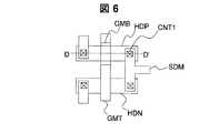
図1は、本発明の画像表示装置の実施例1を説明する画素部を構成する薄膜トランジスタ付近の断面図である。D−D’断面はpチャネルTFTの部分、E−E’断面はnチャネルTFTの部分と画素電極の部分である。本発明の実施例1における画像表示装置の回路構成は図2と同様である。周辺駆動回路を構成するCMOS2の平面図、および画素3の平面図をそれぞれ図6、図7に示す。これらのCMOSおよび画素部の製造方法を図6中のD−D’断面図、図7中のE−E’断面図を用いて図8A〜図8Dおよび図9A〜図9Fに従って説明する。 FIG. 1 is a cross-sectional view of the vicinity of a thin film transistor that constitutes a pixel portion for explaining a first embodiment of the image display device of the present invention. The D-D 'section is a p-channel TFT portion, and the E-E' section is an n-channel TFT portion and a pixel electrode portion. The circuit configuration of the image display apparatus according to the first embodiment of the present invention is the same as that shown in FIG. A plan view of the
ガラス基板SUB上にバッファ層として酸化シリコン膜BUFを100nm堆積し、さらにプラズマCVD法によりアモルファスシリコン層を50nm堆積する。次にXeClエキシマレーザを照射しアモルファスシリコン層を結晶化し、公知のフォトフォトリソグラフィ−エッチング工程(フォト工程1)により、島状のポリシリコン層PSIを得る。その後、プラズマCVD法によりゲート絶縁膜OX1を100nm堆積し、nチャネルTFTのしきい値調整のためボロンイオンを打ち込む(図9A)。 A silicon oxide film BUF is deposited to a thickness of 100 nm as a buffer layer on the glass substrate SUB, and an amorphous silicon layer is deposited to a thickness of 50 nm by plasma CVD. Next, the amorphous silicon layer is crystallized by irradiation with a XeCl excimer laser, and an island-shaped polysilicon layer PSI is obtained by a known photolithography-etching process (photo process 1). Thereafter, a gate insulating film OX1 is deposited to 100 nm by plasma CVD, and boron ions are implanted to adjust the threshold value of the n-channel TFT (FIG. 9A).
その後、膜厚30nmのITOと膜厚150nmのタングステンからなる積層金属膜を堆積する。公知のフォトリソグラフィ工程(フォト工程2)によりゲート電極GM、ゲート線GLおよび画素電極PXをパターンニングするレジストマスクを形成し、公知のウェットエッチングにより、ゲート上層電極GMT(タングステン)にサイドエッチングを施し、レジストに対し0.5μm〜1.0μmの縮小加工を行なう(図9B)。 Thereafter, a laminated metal film made of ITO having a thickness of 30 nm and tungsten having a thickness of 150 nm is deposited. A resist mask for patterning the gate electrode GM, the gate line GL, and the pixel electrode PX is formed by a known photolithography process (Photo process 2), and side etching is performed on the gate upper layer electrode GMT (tungsten) by a known wet etching. Then, the resist is reduced to 0.5 μm to 1.0 μm (FIG. 9B).
次に、レジストをマスクとして、リンのイオン打ち込みによって高濃度n型ポリシリコン層HDNを形成する。レジストを除去し、ゲート上層電極GTMをマスクとしてITOを除去した後、リンのイオン打ち込みによって低濃度n型ポリシリコン層LDNを形成する(図9C)および(図8A、図8B)。 Next, a high concentration n-type polysilicon layer HDN is formed by ion implantation of phosphorus using the resist as a mask. After removing the resist and removing the ITO using the gate upper layer electrode GTM as a mask, a low concentration n-type polysilicon layer LDN is formed by phosphorus ion implantation (FIG. 9C) and (FIGS. 8A and 8B).
次に、公知のフォトリソグラフィ工程により、nチャネルTFTの領域をレジストで覆い(フォト工程3)、レジストをマスクとして、ボロンのイオン打ち込みによって高濃度p型ポリシリコン層HDPを形成する(図9D)。ゲート上層電極GMTおよび画素電極上部のタングステンを除去し、pチャネルTFTのゲート電極GMBおよび画素電極PXを形成する(図9E)。その後、pチャネルTFTのしきい値調整のためリンイオンを打ち込む。この時、pチャネルTFTのゲート電極であるゲート下層電極GMBは30nmと薄いため、ゲート下層電極下のポリシリコン層PSIにリンイオンが打ち込まれる。また、この時、高濃度p型ポリシリコン層HDPにもリンイオンが打ち込まれるが、高濃度p型ポリシリコン層のボロン濃度に比べ、打ち込まれるリンイオンの濃度が十分に低いため、高濃度p型ポリシリコン層HDPの抵抗はほとんど変化しない。 Next, the n-channel TFT region is covered with a resist by a known photolithography process (photo process 3), and a high-concentration p-type polysilicon layer HDP is formed by boron ion implantation using the resist as a mask (FIG. 9D). . The gate upper layer electrode GMT and the tungsten above the pixel electrode are removed to form the gate electrode GMB and the pixel electrode PX of the p-channel TFT (FIG. 9E). Thereafter, phosphorus ions are implanted to adjust the threshold value of the p-channel TFT. At this time, since the gate lower layer electrode GMB which is a gate electrode of the p-channel TFT is as thin as 30 nm, phosphorus ions are implanted into the polysilicon layer PSI under the gate lower layer electrode. At this time, phosphorus ions are also implanted into the high-concentration p-type polysilicon layer HDP, but the concentration of phosphorus ions implanted is sufficiently lower than the boron concentration of the high-concentration p-type polysilicon layer. The resistance of the silicon layer HDP hardly changes.
その後、全体を覆うようにプラズマCVD法により酸化シリコンからなる層間絶縁膜OX2および窒化シリコンからなる保護絶縁膜PASを形成し、公知のフォトフォトリソグラフィ−エッチング工程(フォト工程4)によりコンタクトホールCNT1を形成する(図8C、図8D)。 Thereafter, an interlayer insulating film OX2 made of silicon oxide and a protective insulating film PAS made of silicon nitride are formed by plasma CVD so as to cover the whole, and the contact hole CNT1 is formed by a known photolithography-etching process (photo process 4). Form (FIGS. 8C and 8D).
さらに、アルミニウムからなる金属層を堆積し、公知のフォトフォトリソグラフィ―エッチング工程(フォト工程5)により、ソース/ドレイン電極SDMおよび信号線SLを形成する(図9F)。ソース/ドレイン電極SDMと高濃度ポリシリコン層との接触抵抗を低減させるため、ソース/ドレイン電極SDMおよび信号線SLは積層構造であり、下層膜にタングステンからなるバリア膜を有する。バリア膜の膜厚は50〜150nm、アルミニウム膜は400nm〜600nmであることが望ましい。 Further, a metal layer made of aluminum is deposited, and a source / drain electrode SDM and a signal line SL are formed by a well-known photolithography-etching process (photo process 5) (FIG. 9F). In order to reduce the contact resistance between the source / drain electrode SDM and the high-concentration polysilicon layer, the source / drain electrode SDM and the signal line SL have a laminated structure, and have a barrier film made of tungsten as a lower layer film. The film thickness of the barrier film is desirably 50 to 150 nm, and the aluminum film is desirably 400 nm to 600 nm.
実施例1に依れば、ゲート下層電極GMBを通してpチャネルTFTのしきい値調整イオン打ち込みを行なうことにより、高濃度p型ポリシリコン層HDPを形成する時のレジストマスクと、pチャネルTFTのしきい値調整イオン打ち込みの際のレジストマスクを共用させることができる。このためフォトリソグラフィ工程を削減できる。この場合、ゲート下層電極GMBの膜厚は20nm〜60nmであることが望ましい。 According to the first embodiment, by performing threshold adjustment ion implantation of the p-channel TFT through the gate lower layer electrode GMB, the resist mask for forming the high-concentration p-type polysilicon layer HDP, and the p-channel TFT It is possible to share a resist mask for threshold adjustment ion implantation. Therefore, the photolithography process can be reduced. In this case, the thickness of the gate lower layer electrode GMB is desirably 20 nm to 60 nm.
さらに実施例1によれば、pチャネルTFTのゲート電極形成時において、ゲート上層電極(タングステン)を除去するのと同時に、画素部のタングステンも除去するため、pチャネルTFTのゲート電極GMBと画素電極PXを同時に形成できる。従って、フォトリソグラフィ工程をさらに削減でき、低コストの画像表示装置を提供できる。 Further, according to the first embodiment, when forming the gate electrode of the p-channel TFT, the tungsten in the pixel portion is also removed simultaneously with the removal of the gate upper layer electrode (tungsten). PX can be formed simultaneously. Therefore, the photolithography process can be further reduced, and a low-cost image display apparatus can be provided.
図10は、本発明の実施例2を説明する図7中のF−F'での断面図である。図10は、実施例1におけるpチャネルTFTのゲート電極形成時において、ゲート上層電極GMT(タングステン)を除去するのと同時に、ゲート線GLと信号線SLの交差部のタングステンも除去した構造である。実施例2によれば、ゲート線GLと信号線SLの交差部におけるゲート線の膜厚を薄くできるため、信号線SLの断線を防止でき、歩留まりが向上する。 FIG. 10 is a cross-sectional view taken along the line FF ′ in FIG. 7 for explaining the second embodiment of the present invention. FIG. 10 shows a structure in which the tungsten at the intersection of the gate line GL and the signal line SL is removed at the same time when the gate upper layer electrode GMT (tungsten) is removed when forming the gate electrode of the p-channel TFT in the first embodiment. . According to the second embodiment, since the thickness of the gate line at the intersection of the gate line GL and the signal line SL can be reduced, the disconnection of the signal line SL can be prevented and the yield is improved.
図11は、本発明の実施例3を説明する図2の画素3に対応する部分の平面図である。CMOS2の平面図は図6と同様である。図12に、図6中のD−D’に対応する断面図、図11中のG−G’に対応する断面図を示す。ソース/ドレイン電極SDMの形成までは、実施例1と同様であるが、実施例3では、ソース/ドレイン電極上にITOからなる上部画素電極PXTを有する。上部画素電極PXTとのコンタクト抵抗を低減するため、ソース/ドレイン電極は上側にもバリア膜を有する。実施例3によれば、画素電極と上部画素電極を用いて光学的に透明な容量素子を形成できるため保持容量の構成部分を透明にすることができ、画素の開口率が向上する。 FIG. 11 is a plan view of a portion corresponding to the
図13は、本発明の実施例4を説明する画像表示装置の回路構成図である。図14は、図13における画素部3の平面図を示す。周辺駆動回路を構成するCMOS2の平面図は図6と同様である。画素部はnチャネルTFTおよびpチャネルTFTおよび有機発光層で構成されている。実施例4における画像表示装置の製造方法を図14中のH−H’断面図、J−J’断面図、K−K’断面図を用いて図15A〜図15Bおよび図16A〜図16Eに従って説明する。 FIG. 13 is a circuit configuration diagram of an image display device for explaining the fourth embodiment of the present invention. FIG. 14 is a plan view of the
実施例4の画像表示装置の製造方法は層間絶縁膜OX2の形成までは実施例1と同様である。すなわち、ガラス基板SUB上にバッファ層として酸化シリコン膜BUFを100nm堆積し、さらにプラズマCVD法によりアモルファスシリコン層を50nm堆積する。次に、XeClエキシマレーザを照射しアモルファスシリコン層を結晶化し、公知のフォトフォトリソグラフィ―エッチング工程(フォト工程1)により島状のポリシリコン層PSIを得る。その後、プラズマCVD法によりゲート絶縁膜OX1を100nm堆積し、nチャネルTFTの閾値調整のためボロン(硼素)イオンを打ち込む(図16A)。 The manufacturing method of the image display device of Example 4 is the same as that of Example 1 until the formation of the interlayer insulating film OX2. That is, a silicon oxide film BUF is deposited to 100 nm as a buffer layer on the glass substrate SUB, and an amorphous silicon layer is deposited to 50 nm by plasma CVD. Next, the amorphous silicon layer is crystallized by irradiating a XeCl excimer laser, and an island-shaped polysilicon layer PSI is obtained by a known photolithography-etching process (photo process 1). Thereafter, a gate insulating film OX1 is deposited to 100 nm by plasma CVD, and boron (boron) ions are implanted to adjust the threshold value of the n-channel TFT (FIG. 16A).
その後、膜厚30nmのITOと膜厚150nmのタングステンからなる積層金属膜を堆積する。公知のフォトリソグラフィ工程(フォト工程2)によりゲート電極GM、ゲート線GL、スイッチ線SWLおよび画素電極PXをパターンニングするレジストマスクを形成し、公知のウェットエッチングにより、ゲート上層電極GMT(タングステン)にサイドエッチングを施し、レジストに対し0.5μm〜1.0μmの縮小加工を行なう。 Thereafter, a laminated metal film made of ITO having a thickness of 30 nm and tungsten having a thickness of 150 nm is deposited. A resist mask for patterning the gate electrode GM, the gate line GL, the switch line SWL, and the pixel electrode PX is formed by a known photolithography process (Photo process 2), and the gate upper layer electrode GMT (tungsten) is formed by a known wet etching. Side etching is performed, and the resist is reduced to 0.5 μm to 1.0 μm.
次に、レジストをマスクとして、リンのイオン打ち込みによって高濃度n型ポリシリコン層HDNを形成する。レジストを除去し、ゲート上層電極GTMをマスクとしてITOを除去した後、リンのイオン打ち込みによって低濃度n型ポリシリコン層LDNを形成する(図16B、および図15A)。 Next, a high concentration n-type polysilicon layer HDN is formed by ion implantation of phosphorus using the resist as a mask. After removing the resist and removing the ITO using the gate upper layer electrode GTM as a mask, a low concentration n-type polysilicon layer LDN is formed by phosphorus ion implantation (FIGS. 16B and 15A).
次に、公知のフォトリソグラフィ工程により、nチャネルTFTの領域をレジストで覆い(フォト工程3)、レジストをマスクとして、ボロンのイオン打ち込みによって高濃度p型ポリシリコン層HDPを形成する。ゲート上層電極GMTおよび画素電極上部のタングステンを除去し、pチャネルTFTのゲート電極GMBおよび画素電極PXを形成する(図16C)。 Next, the n-channel TFT region is covered with a resist by a known photolithography process (photo process 3), and a high-concentration p-type polysilicon layer HDP is formed by boron ion implantation using the resist as a mask. The gate upper layer electrode GMT and the tungsten above the pixel electrode are removed to form the gate electrode GMB and the pixel electrode PX of the p-channel TFT (FIG. 16C).
その後、pチャネルTFTの閾値調整のためリンイオンを打ち込む。この時、pチャネルTFTのゲート電極であるゲート下層電極GMBは30nmと薄いため、ゲート下層電極下のポリシリコン層PSIにリンイオンが打ち込まれる。またこの時、高濃度p型ポリシリコン層HDPにもリンイオンが打ち込まれるが、高濃度p型ポリシリコン層のボロン濃度に比べ、打ち込まれるリンイオンの濃度が十分に低いため、高濃度p型ポリシリコン層HDPの抵抗はほとんど変化しない。 Thereafter, phosphorus ions are implanted to adjust the threshold value of the p-channel TFT. At this time, since the gate lower layer electrode GMB which is a gate electrode of the p-channel TFT is as thin as 30 nm, phosphorus ions are implanted into the polysilicon layer PSI under the gate lower layer electrode. At this time, phosphorus ions are also implanted into the high-concentration p-type polysilicon layer HDP, but the concentration of phosphorus ions implanted is sufficiently lower than the boron concentration of the high-concentration p-type polysilicon layer. The resistance of the layer HDP hardly changes.
レジストPST除去の後、全体を覆うようにプラズマCVD法により酸化シリコンからなる層間絶縁膜OX2を形成し、公知のフォトフォトリソグラフィ−エッチング工程(フォト工程4)によりコンタクトホールCNT1を形成する(図15B)。さらに、アルミニウムからなる金属層を堆積し、公知のフォトフォトリソグラフィ−エッチング工程(フォト工程5)により、ソース/ドレイン電極SDM、信号線SLおよび電源線VLを形成する(図16D)。 After removing the resist PST, an interlayer insulating film OX2 made of silicon oxide is formed by plasma CVD so as to cover the whole, and a contact hole CNT1 is formed by a well-known photolithography-etching process (photo process 4) (FIG. 15B). ). Further, a metal layer made of aluminum is deposited, and a source / drain electrode SDM, a signal line SL, and a power supply line VL are formed by a well-known photolithography-etching process (photo process 5) (FIG. 16D).
ソース/ドレイン電極SDMと高濃度ポリシリコン層との接触抵抗を低減させるため、ソース/ドレイン電極SDMおよび信号線SLは積層構造であり、下層膜にタングステンからなるバリア膜を有する。バリア膜の膜厚は50〜150nm、アルミニウム膜は400nm〜600nmであることが望ましい。その後、窒化シリコンからなる保護絶縁膜PASを形成し、公知のフォトフォトリソグラフィ−エッチング工程(フォト工程6)により画素電極上の保護絶縁膜PASを除去する。公知のマスク蒸着により、有機材料からなる発光層OLEDを堆積し、さらにアルミニウムからなる上部画素電極PXTを形成する(図16E)。 In order to reduce the contact resistance between the source / drain electrode SDM and the high-concentration polysilicon layer, the source / drain electrode SDM and the signal line SL have a laminated structure, and have a barrier film made of tungsten as a lower layer film. The film thickness of the barrier film is desirably 50 to 150 nm, and the aluminum film is desirably 400 nm to 600 nm. Thereafter, a protective insulating film PAS made of silicon nitride is formed, and the protective insulating film PAS on the pixel electrode is removed by a known photolithography-etching process (photo process 6). A light emitting layer OLED made of an organic material is deposited by a known mask vapor deposition, and an upper pixel electrode PXT made of aluminum is formed (FIG. 16E).
実施例4によれば、ガラス基板上に有機材料からなる発光層OLEDを有するため、液晶表示装置よりも視野角依存性および動画表示に優れた画像表示装置を提供できる。さらに、液晶表示装置はガラス基板を2枚必要とするのに対し、本実施例の画像表示装置は1枚のガラス基板で装置を構成できるため、薄型の画像表示装置を提供できる。 According to Example 4, since it has the light emitting layer OLED which consists of organic materials on a glass substrate, the image display apparatus excellent in viewing angle dependency and a moving image display can be provided rather than a liquid crystal display device. Further, while the liquid crystal display device requires two glass substrates, the image display device of the present embodiment can be configured with a single glass substrate, so that a thin image display device can be provided.
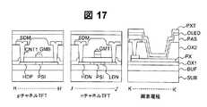
図17は、本発明の実施例5を説明する図14中のH−H’断面図、J−J’断面図、K−K’断面図に対応する断面図である。図17は、実施例4において保護絶縁膜PASと画素電極PXとが接することのないように保護絶縁膜PASをパターンニングし、その後、有機材料からなる発光層OLEDを形成した構造である。本実施例によれば、画素電極PXの上部と層間絶縁膜OX2の側部および上部に接するように有機材料からなる発光層OLEDを形成することにより、発光面積を広くでき、画素の開口率が向上する。 FIG. 17 is a cross-sectional view corresponding to the H-H ′ cross-sectional view, J-J ′ cross-sectional view, and K-K ′ cross-sectional view in FIG. 14 for explaining the fifth embodiment of the present invention. FIG. 17 shows a structure in which the protective insulating film PAS is patterned so that the protective insulating film PAS and the pixel electrode PX are not in contact with each other in Example 4, and then a light emitting layer OLED made of an organic material is formed. According to the present embodiment, by forming the light emitting layer OLED made of an organic material so as to be in contact with the upper portion of the pixel electrode PX and the side portion and the upper portion of the interlayer insulating film OX2, the light emitting area can be increased and the aperture ratio of the pixel can be increased. improves.
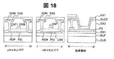
図18は、本発明の実施例6を説明する図14中のH−H’断面図、J−J’断面図、K−K’断面図に対応する断面図である。図18は、実施例4においてソース/ドレイン電極SDMを形成の後、保護絶縁膜PASとして、陽極酸化法によりソース/ドレイン電極の表面に酸化アルミニウム膜を形成し、その後、有機材料からなる発光層を形成した構造である。ソース/ドレイン電極の上層膜はアルミニウム膜であるため、陽極酸化により酸化アルミニウムが形成される。実施例6に依れば、保護絶縁膜PASをパターンニングするフォトフォトリソグラフィ−エッチング工程を削減できるため、より低コストの画像表示装置を提供できる。 18 is a cross-sectional view corresponding to the H-H ′ cross-sectional view, J-J ′ cross-sectional view, and K-K ′ cross-sectional view in FIG. 14 for explaining the sixth embodiment of the present invention. In FIG. 18, after forming the source / drain electrode SDM in Example 4, an aluminum oxide film is formed on the surface of the source / drain electrode by the anodic oxidation method as the protective insulating film PAS, and then the light emitting layer made of an organic material It is the structure which formed. Since the upper layer film of the source / drain electrode is an aluminum film, aluminum oxide is formed by anodic oxidation. According to the sixth embodiment, a photo-photolithography-etching process for patterning the protective insulating film PAS can be reduced, so that a lower cost image display device can be provided.
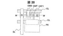
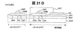
実施例7における画像表示装置の構成図は図2と同様である。周辺駆動回路を構成するCMOS2の平面図および画素3の平面図をそれぞれ図19、図20に示す。実施例7における画像表示装置の製造方法を図19中のL−L’断面図、図20中のM−M’断面図を用いて図21A〜図21Fに従って説明する。 The configuration diagram of the image display apparatus in the seventh embodiment is the same as that in FIG. A plan view of the
図21A〜図21Fは、本発明の画像表示装置の実施例7の製造工程を説明する断面図である。まず、実施例1と同様に、ガラス基板SUB上にバッファ層として酸化シリコン膜BUFを100nm堆積し、さらにプラズマCVD法によりアモルファスシリコン層を50nm堆積する。次にXeClエキシマレーザを照射しアモルファスシリコン層を結晶化し、公知のフォトフォトリソグラフィ−エッチング工程(フォト工程1)により、島状のポリシリコン層PSIを得る。 21A to 21F are cross-sectional views illustrating the manufacturing process of the image display device according to the seventh embodiment of the present invention. First, as in Example 1, a silicon oxide film BUF is deposited as a buffer layer to a thickness of 100 nm on the glass substrate SUB, and an amorphous silicon layer is deposited to a thickness of 50 nm by plasma CVD. Next, the amorphous silicon layer is crystallized by irradiation with a XeCl excimer laser, and an island-shaped polysilicon layer PSI is obtained by a known photolithography-etching process (photo process 1).
その後、プラズマCVD法によりゲート絶縁膜OX1を100nm堆積し、nチャネルTFTのしきい値調整のためボロンイオンを打ち込む。その後、膜厚50nmのITOと膜厚150nmのタングステンからなる積層金属膜を堆積する。公知のフォトリソグラフィ工程(フォト工程2)によりゲート電極GM、ゲート線GLおよび画素電極PXをパターンニングするレジストマスクを形成し、公知のウェットエッチングにより、ゲート上層電極GMT(タングステン)にサイドエッチングを施し、レジストに対し0.5μm〜1.0μmの縮小加工を行なう(図21A)。 Thereafter, a gate insulating film OX1 is deposited to a thickness of 100 nm by plasma CVD, and boron ions are implanted to adjust the threshold value of the n-channel TFT. Thereafter, a laminated metal film made of ITO having a thickness of 50 nm and tungsten having a thickness of 150 nm is deposited. A resist mask for patterning the gate electrode GM, the gate line GL, and the pixel electrode PX is formed by a known photolithography process (Photo process 2), and side etching is performed on the gate upper layer electrode GMT (tungsten) by a known wet etching. Then, the resist is reduced by 0.5 μm to 1.0 μm (FIG. 21A).
次に、公知のエッチングにより、レジストをマスクとしてITOを除去する(図21B)。ゲート上層電極GMTをマスクとして、リンのイオン打ち込みによって高濃度n型ポリシリコン層HDNと低濃度p型ポリシリコン層LDNを形成する。ゲート下層電極GMBを通してイオン打ち込みを行なうため、ゲート下層電極の下側はリンイオン濃度が低くなり、一度のイオン打ち込みにより高濃度n型ポリシリコン層HDNと低濃度n型ポリシリコン層LDNを同時に形成できる(図21C)。 Next, ITO is removed by a known etching using the resist as a mask (FIG. 21B). Using the gate upper layer electrode GMT as a mask, a high concentration n-type polysilicon layer HDN and a low concentration p-type polysilicon layer LDN are formed by phosphorus ion implantation. Since the ion implantation is performed through the gate lower layer electrode GMB, the phosphorus ion concentration is lowered on the lower side of the gate lower layer electrode, and the high concentration n-type polysilicon layer HDN and the low concentration n-type polysilicon layer LDN can be simultaneously formed by one ion implantation. (FIG. 21C).
次に、公知のフォトリソグラフィ工程により、nチャネルTFTの領域をレジストで覆い(フォト工程3)、レジストをマスクとして、ボロンのイオン打ち込みによって高濃度p型ポリシリコン層HDPおよび低濃度p型ポリシリコン層LDPを形成する(図21D)。ゲート上層電極GMTおよび画素電極上部のタングステンを除去し、pチャネルTFTのゲート電極GMBおよび画素電極PXを形成する(図21E)。 Next, the n-channel TFT region is covered with a resist by a well-known photolithography process (photo process 3), and using the resist as a mask, high-concentration p-type polysilicon layer HDP and low-concentration p-type polysilicon are formed by boron ion implantation. A layer LDP is formed (FIG. 21D). The gate upper layer electrode GMT and the tungsten above the pixel electrode are removed to form the gate electrode GMB and the pixel electrode PX of the p-channel TFT (FIG. 21E).
さらに、pチャネルTFTのしきい値調整のためリンイオンを打ち込む。この時、ゲート下層電極GMBは50nmと薄いため、ゲート下層電極下のポリシリコン層PSIにリンイオンが打ち込まれる。またこの時、高濃度p型ポリシリコン層HDPおよび低濃度p型ポリシリコン層LDPにもリンイオンが打ち込まれるが、高濃度p型ポリシリコン層および低濃度p型ポリシリコン層LDPのボロン濃度に比べ、打ち込まれるリンイオンの濃度が十分に低いため、高濃度p型ポリシリコン層HDPおよび低濃度p型ポリシリコン層LDPの抵抗はほとんど変化しない。 Further, phosphorus ions are implanted to adjust the threshold value of the p-channel TFT. At this time, since the gate lower layer electrode GMB is as thin as 50 nm, phosphorus ions are implanted into the polysilicon layer PSI under the gate lower layer electrode. At this time, phosphorus ions are also implanted into the high concentration p-type polysilicon layer HDP and the low concentration p-type polysilicon layer LDP, but compared with the boron concentration of the high concentration p-type polysilicon layer and the low concentration p-type polysilicon layer LDP. Since the concentration of implanted phosphorus ions is sufficiently low, the resistance of the high concentration p-type polysilicon layer HDP and the low concentration p-type polysilicon layer LDP hardly changes.
その後、全体を覆うようにプラズマCVD法により層間絶縁膜OX2および保護絶縁膜PASを形成し、公知のフォトフォトリソグラフィ−エッチング工程(フォト工程4)によりコンタクトホールCNT1を形成する。さらにアルミニウムからなる金属層を堆積し、公知のフォトフォトリソグラフィ−エッチング工程(フォト工程5)により、ソース/ドレイン電極SDMおよび信号線SLを形成する(図21F)。ソース/ドレイン電極SDMと高濃度ポリシリコン層との接触抵抗を低減させるため、ソース/ドレイン電極SDMおよび信号線SLは積層構造であり、下層膜にタングステンからなるバリア膜を有する。バリア膜の膜厚は50〜150nm、アルミニウム膜は400nm〜600nmであることが望ましい。 Thereafter, an interlayer insulating film OX2 and a protective insulating film PAS are formed by plasma CVD so as to cover the entire surface, and a contact hole CNT1 is formed by a known photolithography-etching process (photo process 4). Further, a metal layer made of aluminum is deposited, and a source / drain electrode SDM and a signal line SL are formed by a known photolithography-etching process (photo process 5) (FIG. 21F). In order to reduce the contact resistance between the source / drain electrode SDM and the high-concentration polysilicon layer, the source / drain electrode SDM and the signal line SL have a laminated structure, and have a barrier film made of tungsten as a lower layer film. The film thickness of the barrier film is desirably 50 to 150 nm, and the aluminum film is desirably 400 nm to 600 nm.
実施例7によれば、低濃度n型ポリシリコン層LDNおよび低濃度p型ポリシリコン層LDPの上部にゲート下層電極GMBを有するため、電気ストレスに対するTFTの信頼性を向上させることができる。 According to the seventh embodiment, since the gate lower layer electrode GMB is provided above the low-concentration n-type polysilicon layer LDN and the low-concentration p-type polysilicon layer LDP, the reliability of the TFT against electric stress can be improved.
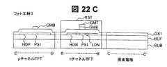
実施例8の画像表示装置の回路構成は図2と同様であり、周辺駆動回路を構成するCMOS2の平面構成および画素3の平面構成はそれぞれ図6、図4と同様である。実施例8における画像表示装置の製造方法を図6中のD−D’断面図、図4中のB−B’断面図、C−C’断面図を用いて図22A〜図22Eに従って説明する。 The circuit configuration of the image display apparatus according to the eighth embodiment is the same as that of FIG. 2, and the planar configuration of the
図22A〜図22Eは、本発明の画像表示装置の実施例8の製造工程を説明する断面図である。ガラス基板SUB上にバッファ層として酸化シリコン膜BUFを100nm堆積し、さらにプラズマCVD法によりアモルファスシリコン層を50nm堆積する。次に、XeClエキシマレーザを照射しアモルファスシリコン層を結晶化し、公知のフォトフォトリソグラフィ−エッチング工程(フォト工程1)により、島状のポリシリコン層PSIを得る。その後、プラズマCVD法によりゲート絶縁膜OX1を100nm堆積し、nチャネルTFTのしきい値調整のためボロンイオンを打ち込む(図22A)。 22A to 22E are cross-sectional views illustrating a manufacturing process of the image display apparatus according to the eighth embodiment of the present invention. A silicon oxide film BUF is deposited to a thickness of 100 nm as a buffer layer on the glass substrate SUB, and an amorphous silicon layer is deposited to a thickness of 50 nm by plasma CVD. Next, the amorphous silicon layer is crystallized by irradiation with a XeCl excimer laser, and an island-shaped polysilicon layer PSI is obtained by a known photolithography-etching process (photo process 1). Thereafter, a gate insulating film OX1 is deposited to a thickness of 100 nm by plasma CVD, and boron ions are implanted to adjust the threshold value of the n-channel TFT (FIG. 22A).
その後、膜厚30nmのチタンと膜厚150nmのタングステンからなる積層金属膜を堆積し、公知のフォトフォトリソグラフィ−エッチング工程(フォト工程2)によりゲート電極GMおよびゲート線GLを形成する。この時、ゲート電極にサイドエッチングを施し、レジストに対し0.5μm〜1.0μmの縮小加工を行なう。次に、レジストをマスクとして、リンのイオン打ち込みによって高濃度n型ポリシリコン層HDNを形成する。レジストを除去し、ゲート上層電極GTMをマスクとしてITOを除去した後、リンのイオン打ち込みによって低濃度n型ポリシリコン層LDNを形成する(図22B)。 Thereafter, a laminated metal film made of titanium with a thickness of 30 nm and tungsten with a thickness of 150 nm is deposited, and a gate electrode GM and a gate line GL are formed by a well-known photolithography-etching process (photo process 2). At this time, the gate electrode is subjected to side etching, and the resist is reduced by 0.5 μm to 1.0 μm. Next, a high concentration n-type polysilicon layer HDN is formed by ion implantation of phosphorus using the resist as a mask. After removing the resist and removing the ITO using the gate upper layer electrode GTM as a mask, a low concentration n-type polysilicon layer LDN is formed by ion implantation of phosphorus (FIG. 22B).
次に、公知のフォトリソグラフィ工程により、nチャネルTFTの領域をレジストで覆い(フォト工程3)、レジストをマスクとして、高濃度p型ポリシリコン層HDPを形成する。さらにゲート上層電極GMTのみを除去し、pチャネルTFTのしきい値調整のためリンイオンを打ち込む(図22C)。この時、ゲート下層電極GMBは30nmと薄いため、ゲート下層電極下のポリシリコン層PSIにリンイオンが打ち込まれる。またこの時、高濃度p型ポリシリコン層HDPにもリンイオンが打ち込まれるが、高濃度p型ポリシリコン層のボロン濃度に比べ、打ち込まれるリンイオンの濃度が十分に低いため、高濃度p型ポリシリコン層HDPの抵抗はほとんど変化しない。 Next, the n-channel TFT region is covered with a resist by a known photolithography process (photo process 3), and a high-concentration p-type polysilicon layer HDP is formed using the resist as a mask. Further, only the gate upper layer electrode GMT is removed, and phosphorus ions are implanted to adjust the threshold value of the p-channel TFT (FIG. 22C). At this time, since the gate lower layer electrode GMB is as thin as 30 nm, phosphorus ions are implanted into the polysilicon layer PSI under the gate lower layer electrode. At this time, phosphorus ions are also implanted into the high-concentration p-type polysilicon layer HDP, but the concentration of phosphorus ions implanted is sufficiently lower than the boron concentration of the high-concentration p-type polysilicon layer. The resistance of the layer HDP hardly changes.
その後、全体を覆うようにプラズマCVD法により層間絶縁膜OX2を形成し、公知のフォトフォトリソグラフィ−エッチング工程(フォト工程4)によりコンタクトホールCNT1を形成する。さらにアルミニウムからなる金属層を堆積し、公知のフォトフォトリソグラフィ−エッチング工程(フォト工程5)により、ソース/ドレイン電極SDMおよび信号線SLを形成する(図22D)。 Thereafter, an interlayer insulating film OX2 is formed by a plasma CVD method so as to cover the entire surface, and a contact hole CNT1 is formed by a known photolithography-etching process (photo process 4). Further, a metal layer made of aluminum is deposited, and a source / drain electrode SDM and a signal line SL are formed by a well-known photolithography-etching process (photo process 5) (FIG. 22D).
その後、全体を覆うように窒化シリコンからなる保護絶縁膜PAS1と有機材料からなる保護絶縁膜PAS2を形成し、公知のフォトフォトリソグラフィ−エッチング工程(フォト工程6)によりコンタクトホールCNT2を形成する。その後、公知のフォトフォトリソグラフィ−エッチング工程(フォト工程7)により、ITOからなる画素電極PXを形成する(図22E)。ソース/ドレイン電極と画素電極および高濃度ポリシリコン層との接触抵抗を低減させるためソース/ドレイン電極SDMおよび信号線SLは上下にタングステンからなるバリア膜を有する。バリア膜の膜厚は50〜150nm、アルミニウム膜は400nm〜600nmであることが望ましい。 Thereafter, a protective insulating film PAS1 made of silicon nitride and a protective insulating film PAS2 made of an organic material are formed so as to cover the whole, and a contact hole CNT2 is formed by a known photolithography-etching process (photo process 6). Thereafter, a pixel electrode PX made of ITO is formed by a known photolithography-etching process (photo process 7) (FIG. 22E). In order to reduce the contact resistance between the source / drain electrode, the pixel electrode, and the high-concentration polysilicon layer, the source / drain electrode SDM and the signal line SL have barrier films made of tungsten on the upper and lower sides. The film thickness of the barrier film is desirably 50 to 150 nm, and the aluminum film is desirably 400 nm to 600 nm.
実施例8によれば、保護絶縁膜PAS2を有機材料で形成することにより、層間絶縁膜OX1よりも比誘電率を低く、膜厚を厚くできる。従って、信号線SLと画素電極との間の寄生容量を小さくでき、高精細な液晶表示装置を提供できる。 According to the eighth embodiment, by forming the protective insulating film PAS2 with an organic material, the relative dielectric constant can be lower than that of the interlayer insulating film OX1, and the film thickness can be increased. Accordingly, the parasitic capacitance between the signal line SL and the pixel electrode can be reduced, and a high-definition liquid crystal display device can be provided.
以上説明した実施例1から実施例8に記載の画像表示装置において、絶縁性基板はガラスに限らず、石英ガラスやプラスチックのような他の絶縁性基板であってもよい。また、バッファ層としては、酸化シリコン膜(SiO)の代わりに窒化シリコン膜(SiN)あるいは酸化シリコン膜と窒化シリコン膜との積層膜を用いても良い。窒化シリコン膜をバッファ層として用いれば、ガラス基板内の不純物がゲート絶縁膜中に拡散侵入するのを効果的に防止できる。 In the image display devices described in the first to eighth embodiments described above, the insulating substrate is not limited to glass, and may be another insulating substrate such as quartz glass or plastic. As the buffer layer, a silicon nitride film (SiN) or a laminated film of a silicon oxide film and a silicon nitride film may be used instead of the silicon oxide film (SiO). If the silicon nitride film is used as a buffer layer, it is possible to effectively prevent impurities in the glass substrate from diffusing and penetrating into the gate insulating film.
アモルファスシリコンの結晶化法は熱アニールによる固相成長法でも良いし、熱アニールとレーザアニールの組み合わせであっても良い。また、半導体膜としては、微結晶シリコンでも良いし、シリコンとゲルマニウムの化合物であっても良く、公知の酸化物半導体であっても良い。 The crystallization method of amorphous silicon may be a solid phase growth method using thermal annealing, or a combination of thermal annealing and laser annealing. The semiconductor film may be microcrystalline silicon, a compound of silicon and germanium, or a known oxide semiconductor.
ソース/ドレイン電極のバリアメタルおよびゲート電極の材料は、Ti、TiW、TiN、W、Cr、Mo、Ta、Nb、V、Zr、Hf、Pt、Ru等の金属、またはそれらの合金でも良い。また画素電極ITOは、公知のZnO系透明電極であっても良い。 The source / drain electrode barrier metal and gate electrode material may be Ti, TiW, TiN, W, Cr, Mo, Ta, Nb, V, Zr, Hf, Pt, Ru, or other metals, or alloys thereof. The pixel electrode ITO may be a known ZnO-based transparent electrode.
実施例2で説明した画像表示装置におけるゲート線GLと信号線SLとの交差部における断面構造は、他の実施例にも同様に適用できる。また、実施例1から実施例7に記載の画像表示装置におけるpチャネルTFTのゲート電極GMBは透明電極(ITO)で形成されているため光を透過する。このため、pチャネルTFTを光センサとして用いると、光の検出効率が向上する。従って本発明は、光検出機能を備えた画像表示装置にも適用できる。 The cross-sectional structure at the intersection of the gate line GL and the signal line SL in the image display device described in the second embodiment can be similarly applied to the other embodiments. Further, since the gate electrode GMB of the p-channel TFT in the image display devices described in the first to seventh embodiments is formed of a transparent electrode (ITO), it transmits light. For this reason, when the p-channel TFT is used as an optical sensor, the light detection efficiency is improved. Therefore, the present invention can also be applied to an image display device having a light detection function.
SUB…絶縁性基板(ガラス基板)、BUF…バッファ層、PSI…ポリシリコン膜、OX1…ゲート絶縁膜、OX2…層間絶縁膜、PAS…保護絶縁膜、PAS1…窒化シリコンからなる保護絶縁膜、PAS2…有機材料からなる保護絶縁膜、GM…ゲート電極、GMT…ゲート上層電極、GMB…ゲート下層電極、SDM…ソース/ドレイン電極、HDN…高濃度n型ポリシリコン層、LDN…低濃度n型ポリシリコン層、HDP…高濃度p型ポリシリコン層、LDP…低濃度p型ポリシリコン層、PSI…ポリシリコン層、CNT1…コンタクトホール、CNT2…コンタクトホール、PX…画素電極、PXT…上部画素電極、OLED…発光層、RST…レジスト、GL…ゲート線、SL…信号線、CL…保持容量線、VL…電源線、SWL…点灯スイッチ線、1…周辺駆動回路、2…CMOS、3…画素、5…液晶容量、6…保持容量、7…発光ダイオード。
SUB ... Insulating substrate (glass substrate), BUF ... Buffer layer, PSI ... Polysilicon film, OX1 ... Gate insulating film, OX2 ... Interlayer insulating film, PAS ... Protective insulating film, PAS1 ... Protective insulating film made of silicon nitride, PAS2 ... protective insulating film made of organic material, GM ... gate electrode, GMT ... gate upper layer electrode, GMB ... gate lower layer electrode, SDM ... source / drain electrode, HDN ... high concentration n-type polysilicon layer, LDN ... low concentration n type poly Silicon layer, HDP: High-concentration p-type polysilicon layer, LDP: Low-concentration p-type polysilicon layer, PSI ... Polysilicon layer, CNT1 ... Contact hole, CNT2 ... Contact hole, PX ... Pixel electrode, PXT ... Upper pixel electrode, OLED ... light emitting layer, RST ... resist, GL ... gate line, SL ... signal line, CL ... retention capacitor line, VL ... power supply line SWL ... lighting switch line, 1 ... peripheral driving circuit, 2 ... CMOS, 3 ... pixels, 5 ... liquid crystal capacitance, 6 ... holding
Claims (11)
Translated fromJapanese前記複数のゲート線は積層構造であり、前記複数の薄膜トランジスタは、nチャネル伝導型およびpチャネル伝導型の2種類からなり、一方の薄膜トランジスタのゲート電極は、前記ゲート線と同じ構成の積層電極で、他方の薄膜トランジスタのゲート電極は前記ゲート線の下層電極と同層の電極であることを特徴とする画像表示装置。An image display device comprising a plurality of gate lines formed on an insulating substrate, a plurality of signal lines formed to intersect the plurality of gate lines in a matrix, and a plurality of thin film transistors,
The plurality of gate lines have a stacked structure, and the plurality of thin film transistors are of two types, n-channel conductivity type and p-channel conductivity type, and the gate electrode of one thin film transistor is a stacked electrode having the same configuration as the gate line. The gate electrode of the other thin film transistor is an electrode in the same layer as the lower layer electrode of the gate line.
前記ゲート線および前記信号線は積層構造であり、前記ゲート線の上層膜と前記信号線の下層膜は同じ材質であることを特徴とする画像表示装置。In claim 1,
The image display device, wherein the gate line and the signal line have a laminated structure, and the upper layer film of the gate line and the lower layer film of the signal line are made of the same material.
前記複数のゲート線と前記複数の信号線とで囲まれた領域に画素電極を有しており、前記ゲート線の下層電極は、前記画素電極と同層の電極であることを特徴とする画像表示装置。In claim 1,
An image having a pixel electrode in a region surrounded by the plurality of gate lines and the plurality of signal lines, wherein the lower layer electrode of the gate line is an electrode in the same layer as the pixel electrode Display device.
前記画素電極および前記ゲート線の下層電極は透明電極であることを特徴とする画像表示装置。In claim 3,
The image display device, wherein the pixel electrode and the lower layer electrode of the gate line are transparent electrodes.
前記画素電極および前記ゲート線の下層電極の膜厚は20nm以上60nm以下であることを特徴とする画像表示装置。In claim 3,
The image display device, wherein the pixel electrode and the lower layer electrode of the gate line have a thickness of 20 nm to 60 nm.
前記ゲート線と前記信号線の間に層間絶縁膜を有しており、前記画素電極の上方に前記層間絶縁膜を介して前記画素電極と同じ材質の電極を有することを特徴とする画像表示装置。In claim 3,
An image display device having an interlayer insulating film between the gate line and the signal line, and having an electrode made of the same material as the pixel electrode via the interlayer insulating film above the pixel electrode .
前記ゲート線と前記信号線との交差部は、基板側から、ゲート線の下層膜/層間絶縁膜/信号線をこの順で積層された構成を有することを特徴とする画像表示装置。In claim 3,
The intersection of the gate line and the signal line has a configuration in which a lower layer film / interlayer insulating film / signal line of the gate line are stacked in this order from the substrate side.
前記信号線の上面に接する保護絶縁膜を有し、前記保護絶縁膜の上面と側面および前記画素電極の上面に接して形成された発光層を有することを特徴とする画像表示装置。In claim 3,
An image display device comprising: a protective insulating film in contact with an upper surface of the signal line; and a light emitting layer formed in contact with the upper surface and side surfaces of the protective insulating film and the upper surface of the pixel electrode.
前記層間絶縁膜はコンタクトホールを有し、前記画素電極の上面および前記層間絶縁膜の上面と側面に接するように形成された発光層を有することを特徴とする画像表示装置。In claim7 ,
2. The image display device according to claim 1, wherein the interlayer insulating film has a contact hole and a light emitting layer formed so as to be in contact with the upper surface of the pixel electrode and the upper surface and side surfaces of the interlayer insulating film.
前記信号線は積層構造であり、前記信号線の表面に当該信号線の上層膜としての酸化膜が形成されていることを特徴とする画像表示装置。In claim 3,
The image display device, wherein the signal line has a laminated structure, and an oxide film as an upper layer film of the signal line is formed on a surface of the signal line.
前記複数のゲート線の上層電極は、前記複数のゲート線の下層電極に対し縮小加工されていることを特徴とする画像表示装置。
In claim 1,
The upper layer electrode of the plurality of gate lines is reduced in size with respect to the lower layer electrode of the plurality of gate lines.
Priority Applications (3)
| Application Number | Priority Date | Filing Date | Title |
|---|---|---|---|
| JP2006125338AJP5060738B2 (en) | 2006-04-28 | 2006-04-28 | Image display device |
| CNB2007101022224ACN100543536C (en) | 2006-04-28 | 2007-04-27 | Image display device and manufacturing method thereof |
| US11/741,272US7550772B2 (en) | 2006-04-28 | 2007-04-27 | Image display device and manufacturing method thereof |
Applications Claiming Priority (1)
| Application Number | Priority Date | Filing Date | Title |
|---|---|---|---|
| JP2006125338AJP5060738B2 (en) | 2006-04-28 | 2006-04-28 | Image display device |
Publications (2)
| Publication Number | Publication Date |
|---|---|
| JP2007298649A JP2007298649A (en) | 2007-11-15 |
| JP5060738B2true JP5060738B2 (en) | 2012-10-31 |
Family
ID=38647504
Family Applications (1)
| Application Number | Title | Priority Date | Filing Date |
|---|---|---|---|
| JP2006125338AActiveJP5060738B2 (en) | 2006-04-28 | 2006-04-28 | Image display device |
Country Status (3)
| Country | Link |
|---|---|
| US (1) | US7550772B2 (en) |
| JP (1) | JP5060738B2 (en) |
| CN (1) | CN100543536C (en) |
Families Citing this family (44)
| Publication number | Priority date | Publication date | Assignee | Title |
|---|---|---|---|---|
| JP5090708B2 (en)* | 2006-10-20 | 2012-12-05 | 株式会社ジャパンディスプレイイースト | Image display device and manufacturing method thereof |
| KR100908236B1 (en)* | 2008-04-24 | 2009-07-20 | 삼성모바일디스플레이주식회사 | OLED display device and manufacturing method thereof |
| KR100958640B1 (en)* | 2008-06-09 | 2010-05-20 | 삼성모바일디스플레이주식회사 | A substrate having a capacitor and a thin film transistor, a flat panel display device having the same, and a method of manufacturing a substrate having the capacitor and a thin film transistor |
| KR101540341B1 (en)* | 2008-10-17 | 2015-07-30 | 삼성전자주식회사 | PANEL STRUCTURE, DISPLAY DEVICE COMPRISING PANEL STRUCTURE AND METHOD FOR MANUFACTURING |
| KR101074788B1 (en)* | 2009-01-30 | 2011-10-20 | 삼성모바일디스플레이주식회사 | Flat panel display apparatus and the manufacturing method thereof |
| US20100224880A1 (en)* | 2009-03-05 | 2010-09-09 | Semiconductor Energy Laboratory Co., Ltd. | Semiconductor device |
| CN101957530B (en)* | 2009-07-17 | 2013-07-24 | 北京京东方光电科技有限公司 | TFT-LCD (Thin Film Transistor-Liquid Crystal Display) array baseplate and manufacturing method thereof |
| TWI604594B (en)* | 2009-08-07 | 2017-11-01 | 半導體能源研究所股份有限公司 | Semiconductor device and telephone, watch, and display device including the same |
| TWI596741B (en) | 2009-08-07 | 2017-08-21 | 半導體能源研究所股份有限公司 | Semiconductor device and method of manufacturing same |
| JP5642447B2 (en)* | 2009-08-07 | 2014-12-17 | 株式会社半導体エネルギー研究所 | Semiconductor device |
| JP5663231B2 (en) | 2009-08-07 | 2015-02-04 | 株式会社半導体エネルギー研究所 | Light emitting device |
| US8115883B2 (en) | 2009-08-27 | 2012-02-14 | Semiconductor Energy Laboratory Co., Ltd. | Display device and method for manufacturing the same |
| WO2011027701A1 (en)* | 2009-09-04 | 2011-03-10 | Semiconductor Energy Laboratory Co., Ltd. | Light-emitting device and method for manufacturing the same |
| WO2011027702A1 (en) | 2009-09-04 | 2011-03-10 | Semiconductor Energy Laboratory Co., Ltd. | Light-emitting device and method for manufacturing the same |
| KR101396096B1 (en) | 2009-10-09 | 2014-05-15 | 가부시키가이샤 한도오따이 에네루기 켄큐쇼 | Semiconductor device and manufacturing method thereof |
| KR101812683B1 (en)* | 2009-10-21 | 2017-12-27 | 가부시키가이샤 한도오따이 에네루기 켄큐쇼 | Method for manufacturing semiconductor device |
| KR101117642B1 (en) | 2009-11-16 | 2012-03-05 | 삼성모바일디스플레이주식회사 | Organic light emitting diode display and method for manufacturing the same |
| KR101048987B1 (en) | 2009-12-10 | 2011-07-12 | 삼성모바일디스플레이주식회사 | Flat panel display and manufacturing method thereof |
| WO2011070901A1 (en)* | 2009-12-11 | 2011-06-16 | Semiconductor Energy Laboratory Co., Ltd. | Semiconductor device and manufacturing method thereof |
| CN101789398B (en)* | 2010-03-09 | 2012-08-22 | 友达光电股份有限公司 | Manufacturing method of semiconductor element |
| KR101692954B1 (en)* | 2010-05-17 | 2017-01-05 | 삼성디스플레이 주식회사 | Organic light emitting display device and manufacturing method of the same |
| JP5714973B2 (en) | 2010-05-21 | 2015-05-07 | 株式会社半導体エネルギー研究所 | Semiconductor device |
| JP5502996B2 (en)* | 2010-05-27 | 2014-05-28 | パナソニック株式会社 | Thin film semiconductor device, display device, and method of manufacturing thin film semiconductor device |
| KR101193197B1 (en)* | 2010-07-07 | 2012-10-19 | 삼성디스플레이 주식회사 | Organinc light emitting display device and manufacturing method for the same |
| US8558960B2 (en) | 2010-09-13 | 2013-10-15 | Semiconductor Energy Laboratory Co., Ltd. | Liquid crystal display device and method for manufacturing the same |
| KR20120063746A (en)* | 2010-12-08 | 2012-06-18 | 삼성모바일디스플레이주식회사 | Organinc light emitting display device and manufacturing method for the same |
| KR20120067153A (en) | 2010-12-15 | 2012-06-25 | 삼성엘이디 주식회사 | Light emitting device, light emitting device package, manufacturing method of light emitting device, and packaging method of light emitting device |
| KR101813492B1 (en)* | 2011-01-05 | 2018-01-02 | 삼성디스플레이 주식회사 | Organic light emitting display device and method for manufacturing the same |
| KR101223725B1 (en)* | 2011-01-10 | 2013-01-17 | 삼성디스플레이 주식회사 | Organic light emitting display device and manufacturing method thereof |
| KR101962850B1 (en)* | 2011-04-22 | 2019-03-28 | 삼성디스플레이 주식회사 | An organic light emitting display device and the manufacturing method thereof |
| KR20120129592A (en)* | 2011-05-20 | 2012-11-28 | 삼성디스플레이 주식회사 | Backplane for flat panel display apparatus, flat panel display apparatus comprising the same, and manufacturing method of the backplane for flat panel display apparatus |
| SG2014013833A (en)* | 2011-06-24 | 2014-10-30 | Sharp Kk | Display device and method for manufacturing same |
| JP5964967B2 (en)* | 2012-08-02 | 2016-08-03 | シャープ株式会社 | Semiconductor device and manufacturing method thereof |
| KR102001057B1 (en) | 2012-10-31 | 2019-07-18 | 엘지디스플레이 주식회사 | Method of fabricating array substrate |
| US9564478B2 (en) | 2013-08-26 | 2017-02-07 | Apple Inc. | Liquid crystal displays with oxide-based thin-film transistors |
| US9818765B2 (en)* | 2013-08-26 | 2017-11-14 | Apple Inc. | Displays with silicon and semiconducting oxide thin-film transistors |
| KR102285384B1 (en)* | 2014-09-15 | 2021-08-04 | 삼성디스플레이 주식회사 | Thin film transistor array substrate and manufacturing method for the same and display |
| KR102360783B1 (en)* | 2014-09-16 | 2022-02-10 | 삼성디스플레이 주식회사 | display device |
| KR102284756B1 (en) | 2014-09-23 | 2021-08-03 | 삼성디스플레이 주식회사 | display device |
| US9543370B2 (en) | 2014-09-24 | 2017-01-10 | Apple Inc. | Silicon and semiconducting oxide thin-film transistor displays |
| US10170711B2 (en)* | 2015-05-05 | 2019-01-01 | Apple Inc. | Display with vias to access driver circuitry |
| US9818344B2 (en) | 2015-12-04 | 2017-11-14 | Apple Inc. | Display with light-emitting diodes |
| JP6725335B2 (en)* | 2016-06-20 | 2020-07-15 | 株式会社ジャパンディスプレイ | Semiconductor device |
| CN107731929B (en)* | 2017-09-28 | 2019-12-13 | 信利(惠州)智能显示有限公司 | Method for manufacturing thin film transistor |
Family Cites Families (4)
| Publication number | Priority date | Publication date | Assignee | Title |
|---|---|---|---|---|
| JPH09191111A (en)* | 1995-11-07 | 1997-07-22 | Semiconductor Energy Lab Co Ltd | Semiconductor device and manufacturing method thereof |
| JPH1096956A (en)* | 1996-09-24 | 1998-04-14 | Toshiba Corp | Liquid crystal display device and method of manufacturing the same |
| US6545359B1 (en)* | 1998-12-18 | 2003-04-08 | Semiconductor Energy Laboratory Co., Ltd. | Wiring line and manufacture process thereof, and semiconductor device and manufacturing process thereof |
| JP4723800B2 (en)* | 2003-08-18 | 2011-07-13 | 東芝モバイルディスプレイ株式会社 | Method for manufacturing array substrate |
- 2006
- 2006-04-28JPJP2006125338Apatent/JP5060738B2/enactiveActive
- 2007
- 2007-04-27CNCNB2007101022224Apatent/CN100543536C/enactiveActive
- 2007-04-27USUS11/741,272patent/US7550772B2/enactiveActive
Also Published As
| Publication number | Publication date |
|---|---|
| US20070252145A1 (en) | 2007-11-01 |
| US7550772B2 (en) | 2009-06-23 |
| CN100543536C (en) | 2009-09-23 |
| JP2007298649A (en) | 2007-11-15 |
| CN101063758A (en) | 2007-10-31 |
Similar Documents
| Publication | Publication Date | Title |
|---|---|---|
| JP5060738B2 (en) | Image display device | |
| JP5090708B2 (en) | Image display device and manufacturing method thereof | |
| JP2008129314A (en) | Image display device and manufacturing method thereof | |
| KR101258474B1 (en) | Semiconductor device and manufacturing method thereof | |
| EP3282483A1 (en) | Pixel unit and method for preparing the same, array substrate and display device | |
| JP5490138B2 (en) | Thin film transistor and manufacturing method thereof, semiconductor device and manufacturing method thereof, and display device | |
| CN102544070B (en) | Microcrystalline thin film transistor, display device including the same, and method of manufacturing the same | |
| JP5138276B2 (en) | Manufacturing method of display device | |
| JP2010206154A (en) | Display device | |
| CN101165908A (en) | TFT substrate, manufacturing method thereof, and displaying device with the TFT substrate | |
| JP4377355B2 (en) | Manufacturing method of semiconductor device | |
| CN1655056B (en) | Optical mask and method for manufacturing thin film transistor array panel using the same | |
| CN100474085C (en) | Thin Film Transistor Array Panel | |
| JP2010243741A (en) | Thin film transistor array substrate, manufacturing method thereof, and liquid crystal display device | |
| CN1670930A (en) | Fabrication method of metal oxide semiconductor with lightly doped drain | |
| JP4563499B2 (en) | Method for manufacturing semiconductor device | |
| JP5507159B2 (en) | Display device and manufacturing method thereof | |
| JP2009289874A (en) | Thin-film transistor and display unit | |
| JP4513361B2 (en) | Semiconductor device, semiconductor device manufacturing method, and electro-optical device | |
| KR20100065739A (en) | Fabricating method of electric device | |
| JPH10209452A (en) | Thin film transistor and its manufacture | |
| JP2007256638A (en) | Thin film transistor substrate and liquid crystal display device using same | |
| JP2009010242A (en) | Display device and manufacturing method thereof | |
| JP2009224396A (en) | Thin film transistor substrate and method of manufacturing the same, and display device | |
| JP2007109876A (en) | Thin film transistor and manufacturing method thereof |
Legal Events
| Date | Code | Title | Description |
|---|---|---|---|
| A621 | Written request for application examination | Free format text:JAPANESE INTERMEDIATE CODE: A621 Effective date:20081217 | |
| A711 | Notification of change in applicant | Free format text:JAPANESE INTERMEDIATE CODE: A712 Effective date:20110218 | |
| RD03 | Notification of appointment of power of attorney | Free format text:JAPANESE INTERMEDIATE CODE: A7423 Effective date:20110218 | |
| A131 | Notification of reasons for refusal | Free format text:JAPANESE INTERMEDIATE CODE: A131 Effective date:20111011 | |
| A521 | Request for written amendment filed | Free format text:JAPANESE INTERMEDIATE CODE: A523 Effective date:20111209 | |
| A131 | Notification of reasons for refusal | Free format text:JAPANESE INTERMEDIATE CODE: A131 Effective date:20120221 | |
| A521 | Request for written amendment filed | Free format text:JAPANESE INTERMEDIATE CODE: A523 Effective date:20120411 | |
| TRDD | Decision of grant or rejection written | ||
| A01 | Written decision to grant a patent or to grant a registration (utility model) | Free format text:JAPANESE INTERMEDIATE CODE: A01 Effective date:20120724 | |
| A01 | Written decision to grant a patent or to grant a registration (utility model) | Free format text:JAPANESE INTERMEDIATE CODE: A01 | |
| A61 | First payment of annual fees (during grant procedure) | Free format text:JAPANESE INTERMEDIATE CODE: A61 Effective date:20120806 | |
| FPAY | Renewal fee payment (event date is renewal date of database) | Free format text:PAYMENT UNTIL: 20150810 Year of fee payment:3 | |
| R150 | Certificate of patent or registration of utility model | Ref document number:5060738 Country of ref document:JP Free format text:JAPANESE INTERMEDIATE CODE: R150 | |
| R250 | Receipt of annual fees | Free format text:JAPANESE INTERMEDIATE CODE: R250 | |
| R250 | Receipt of annual fees | Free format text:JAPANESE INTERMEDIATE CODE: R250 | |
| R250 | Receipt of annual fees | Free format text:JAPANESE INTERMEDIATE CODE: R250 | |
| R250 | Receipt of annual fees | Free format text:JAPANESE INTERMEDIATE CODE: R250 | |
| R250 | Receipt of annual fees | Free format text:JAPANESE INTERMEDIATE CODE: R250 | |
| R250 | Receipt of annual fees | Free format text:JAPANESE INTERMEDIATE CODE: R250 | |
| S531 | Written request for registration of change of domicile | Free format text:JAPANESE INTERMEDIATE CODE: R313531 | |
| S533 | Written request for registration of change of name | Free format text:JAPANESE INTERMEDIATE CODE: R313533 | |
| R350 | Written notification of registration of transfer | Free format text:JAPANESE INTERMEDIATE CODE: R350 | |
| R250 | Receipt of annual fees | Free format text:JAPANESE INTERMEDIATE CODE: R250 | |
| R250 | Receipt of annual fees | Free format text:JAPANESE INTERMEDIATE CODE: R250 | |
| R250 | Receipt of annual fees | Free format text:JAPANESE INTERMEDIATE CODE: R250 | |
| S111 | Request for change of ownership or part of ownership | Free format text:JAPANESE INTERMEDIATE CODE: R313117 | |
| R350 | Written notification of registration of transfer | Free format text:JAPANESE INTERMEDIATE CODE: R350 | |
| R250 | Receipt of annual fees | Free format text:JAPANESE INTERMEDIATE CODE: R250 | |
| S111 | Request for change of ownership or part of ownership | Free format text:JAPANESE INTERMEDIATE CODE: R313117 | |
| R250 | Receipt of annual fees | Free format text:JAPANESE INTERMEDIATE CODE: R250 | |
| R350 | Written notification of registration of transfer | Free format text:JAPANESE INTERMEDIATE CODE: R350 |