JP5058046B2 - Display device with built-in optical sensor - Google Patents
Display device with built-in optical sensorDownload PDFInfo
- Publication number
- JP5058046B2 JP5058046B2JP2008091784AJP2008091784AJP5058046B2JP 5058046 B2JP5058046 B2JP 5058046B2JP 2008091784 AJP2008091784 AJP 2008091784AJP 2008091784 AJP2008091784 AJP 2008091784AJP 5058046 B2JP5058046 B2JP 5058046B2
- Authority
- JP
- Japan
- Prior art keywords
- tft
- photoelectric conversion
- channel layer
- optical sensor
- built
- Prior art date
- Legal status (The legal status is an assumption and is not a legal conclusion. Google has not performed a legal analysis and makes no representation as to the accuracy of the status listed.)
- Expired - Fee Related
Links
Images


Landscapes
- Liquid Crystal (AREA)
- Devices For Indicating Variable Information By Combining Individual Elements (AREA)
- Solid State Image Pick-Up Elements (AREA)
- Light Receiving Elements (AREA)
- Position Input By Displaying (AREA)
- Thin Film Transistor (AREA)
Description
Translated fromJapanese本発明は、表示画面への指押しの検出に適用可能な光センサを各画素部に備えた光センサ内蔵表示装置に関する。 The present invention relates to a display device with a built-in optical sensor provided with a photosensor applicable to detection of a finger press on a display screen in each pixel portion.
特許文献1には、光電変換素子として非晶質シリコンTFT(TFT:薄膜トランジスタ)を用いた2次元光センサを有する光センサ内蔵表示装置が開示されている。この表示装置は、液晶表示部の画素と光センサ部の画素とを一致させ、液晶駆動用TFTと光センサ用TFTの各々のゲート絶縁膜/チャネル層の積層構造を同時に形成することを特徴とするものである。またTFTアレイ基板の各画素内には、液晶駆動用TFTと、光センサ用TFTと、蓄積容量とが設けられている。また液晶表示部の周辺回路(走査回路など)は、TFTアレイ基板の外部回路として備えられている。
また特許文献2には、光電変換素子を内蔵したTFTアレイ基板を有する光センサ内蔵表示装置が開示されている。この表示装置は、透明基板上に、多結晶半導体層を含む活性層を有する表示用TFT(即ち多結晶シリコンTFT)と、光電変換層が非晶質シリコン膜で構成された光電変換素子(即ち非晶質シリコンTFT)とを備えており、前記多結晶シリコンTFTの活性層の下層に形成された非晶質シリコン膜と、前記光電変換素子の前記非晶質シリコン膜とを同一工程で形成することを特徴とするものである。またTFTアレイ基板の各画素内には、前記表示用TFTと、前記光電変換素子と、補助容量電極と、蓄積容量電極とが設けられている。
一般に、上記の様な光センサ内蔵表示装置の当該光センサ(光電変換素子)は、表示画面への指押しの検出(タッチセンサ)に使用される。この場合のタッチセンサの検出方式には、下記の2つの方式がある。1つは、表示画面から射光されるバックライト光の指での反射光を当該光電変換素子で検出する方式(反射方式)である。もう1つは、外部から表示画面に入射する外光(例えば太陽光)が指で遮光されたことを当該光電変換素子で検出する方式(遮光方式)である。 Generally, the optical sensor (photoelectric conversion element) of the display device with a built-in optical sensor as described above is used for detection of a finger press on the display screen (touch sensor). In this case, there are the following two methods for detecting the touch sensor. One is a method (reflection method) in which reflected light from a finger of backlight light emitted from the display screen is detected by the photoelectric conversion element. The other is a method (light-shielding method) in which the photoelectric conversion element detects that external light (for example, sunlight) incident on the display screen from the outside is shielded by a finger.
しかし従来の光センサ内蔵表示装置では、上記の様に光電変換素子として非晶質シリコンTFTのみを使用しているので、下記(1)(2)の問題があった。 However, since the conventional photosensor built-in display device uses only the amorphous silicon TFT as the photoelectric conversion element as described above, there are the following problems (1) and (2).
(1)反射方式の場合は、バックライト光の輝度が低く設定されると、光センサの検出精度が低下する。この改善策として、補助光源を備えて、バックライト光に補助光源からの補助光を重ねることで、指での反射光の輝度を高くして、光センサの検出精度を向上させる事が考えられる。 (1) In the case of the reflection method, when the brightness of the backlight light is set low, the detection accuracy of the optical sensor is lowered. As an improvement measure, it is conceivable to provide an auxiliary light source and superimpose the auxiliary light from the auxiliary light source on the backlight light, thereby increasing the brightness of the reflected light from the finger and improving the detection accuracy of the optical sensor. .
しかし従来では、上記の様に光電変換素子として非晶質シリコンTFTのみを使用しているので、可視光しか検出できない。そのため、補助光を可視光にする必要があり、そうすると、補助光によりバックライト光が強められ、実質的にバックライト光の輝度を低く設定できなくなる(即ち表示画面の輝度設定に影響を与えずに光センサの検出精度を向上できない)という問題があった。 However, conventionally, since only an amorphous silicon TFT is used as a photoelectric conversion element as described above, only visible light can be detected. For this reason, it is necessary to make the auxiliary light visible, and the backlight light is strengthened by the auxiliary light, and the luminance of the backlight light cannot be set substantially low (that is, the luminance setting of the display screen is not affected). However, the detection accuracy of the optical sensor cannot be improved.
(2)遮光方式の場合は、従来では、上記の様に光電変換素子として非晶質シリコンTFTのみを使用しており、可視光しか検出できないので、光電変換素子により、バックライト光の表示装置内部での反射光が検出され、太陽光だけを正確に検出できず、タッチセンサの検出精度が低下するという問題があった。 (2) In the case of the light shielding method, conventionally, only an amorphous silicon TFT is used as a photoelectric conversion element as described above, and only visible light can be detected. There is a problem in that reflected light inside is detected, and only sunlight is not accurately detected, and the detection accuracy of the touch sensor is lowered.
また光電変換素子は、非晶質シリコンTFTで構成されるので、その光感度の安定性が悪く、その光感度が動作時のストレスによって時間と共に変化し、光センサの検出精度が低下するという問題があった。 In addition, since the photoelectric conversion element is composed of amorphous silicon TFTs, the stability of the photosensitivity is poor, the photosensitivity changes with time due to stress during operation, and the detection accuracy of the photosensor decreases. was there.
また、TFTとして非晶質シリコンTFTのみを用いたTFTアレイ基板では、一般に非晶質シリコンTFTの移動度は小さいので、その非晶質シリコンTFTを用いて、液晶表示部の周辺回路(光センサ信号読出回路や走査回路など)をTFTアレイ基板上に形成できない。従って、周辺回路を外部回路として備える必要がある。そのため、回路規模が増大するという問題や、実装工程での歩留の低下により製造コストが増大するという問題があった。 Moreover, in a TFT array substrate using only amorphous silicon TFTs as TFTs, the mobility of amorphous silicon TFTs is generally small, so that peripheral circuits (optical sensors) of a liquid crystal display unit are used by using the amorphous silicon TFTs. Signal readout circuit, scanning circuit, etc.) cannot be formed on the TFT array substrate. Therefore, it is necessary to provide a peripheral circuit as an external circuit. For this reason, there has been a problem that the circuit scale is increased and a manufacturing cost is increased due to a decrease in yield in the mounting process.
他方、特許文献2では、TFTアレイ基板上に多結晶シリコンTFTが設けられており、一般に多結晶シリコンTFTの移動度は大きいので、その多結晶シリコンTFTを用いて、周辺回路をTFTアレイ基板上に形成できる。そのため、上記の回路規模の増大や製造コストの問題を解決できる。 On the other hand, in
しかしながら、特許文献2では、多結晶シリコンTFTの下層に非晶質シリコン膜が形成されるので、非晶質シリコン膜は、多結晶シリコンTFTの製造工程の影響を受ける。即ち多結晶シリコンTFTの製造工程では、ゲート絶縁膜や層間絶縁膜の形成時に400℃以上の加熱工程があるため、この加熱工程により非晶質シリコン膜中の水素が離脱し、欠陥準位が増加し、非晶質シリコン膜の光感度が低下するという問題があった。 However, in
また液晶表示装置では、一般的にカラーフィルタ基板を前面側に配置し、TFTアレイ基板をバックライト側に配置することが多い。しかし、例えば特許文献2の様にトップゲート構造の光電変換用TFTの場合には、TFTアレイ基板を前面側に配置する必要がある。そのため、外光がTFTアレイ基板上の配線やTFTの電極で反射し、その反射光により表示特性が低下するという問題があった。 Further, in a liquid crystal display device, in general, a color filter substrate is generally arranged on the front side, and a TFT array substrate is often arranged on the backlight side. However, in the case of a photoelectric conversion TFT having a top gate structure as in
また上記(2)の問題と類似するが、光電変換層に非晶質シリコン膜を用いて、可視光の中心となる550nm〜600nmの波長帯域の光を受光できる様にすることで、高感度の光電変換素子を得ることができる。しかし、太陽光の様な可視光と近赤外光とを含む光だけを検出できないので、上記の遮光方式の場合には、バックライト光の影響を受けや易くなり、光センサのS/N比が低下する(即ち誤動作を引き起こす)という問題があった。 Although similar to the problem (2) above, it is possible to receive light in a wavelength band of 550 nm to 600 nm, which is the center of visible light, by using an amorphous silicon film for the photoelectric conversion layer, thereby achieving high sensitivity. Can be obtained. However, since only light including visible light and near-infrared light such as sunlight cannot be detected, in the case of the above-described light shielding method, it is easily affected by backlight light, and the S / N of the optical sensor is increased. There is a problem that the ratio is lowered (that is, it causes a malfunction).
この発明は、上記のような問題点を解消するために成されたものであり、第1に、表示画面の輝度設定に影響を与えずに光センサの検出精度を向上できる光センサ内蔵表示装置を提供すること、第2に、太陽光の様な可視光と近赤外光とを含む光だけを検出できる光内蔵用表示装置を提供すること、第3に、回路規模の増大を防止し且つ製造コストを低減できる光内蔵用表示装置を提供することを目的とする。 The present invention has been made to solve the above-described problems. First, a display device with a built-in photosensor that can improve the detection accuracy of the photosensor without affecting the luminance setting of the display screen. Second, providing a display device with built-in light that can detect only light including visible light and near infrared light such as sunlight, and thirdly, preventing an increase in circuit scale It is another object of the present invention to provide a display device with a built-in light that can reduce the manufacturing cost.
上記課題を解決する為に、本発明の第1の形態は、TFT(TFT:薄膜トランジスタ)アレイ基板の各画素部に、微結晶シリコンTFTで構成された画素駆動用TFTと、微結晶シリコンTFT(即ち近赤外光の入射でオン駆動するTFT)で構成された第1の光電変換用TFTと、非晶質シリコンTFT(即ち可視光の入射でオン駆動するTFT)で構成され、前記第1の光電変換用TFTと並列接続された第2の光電変換用TFTと、を備えるものである。 In order to solve the above-described problems, a first embodiment of the present invention is a pixel driving TFT composed of a microcrystalline silicon TFT and a microcrystalline silicon TFT ( That is, it is composed of a first photoelectric conversion TFT composed of a TFT that is turned on by the incidence of near infrared light and an amorphous silicon TFT (that is, a TFT that is turned on by the incidence of visible light). And a second photoelectric conversion TFT connected in parallel with the photoelectric conversion TFT.
また本発明の第2の形態は、TFTアレイ基板の各画素部に、微結晶シリコンTFTで構成された画素駆動用TFTと、微結晶シリコンTFTで構成された第1の光電変換用TFTと、非晶質シリコンTFTで構成され、前記第1の光電変換用TFTと直列接続された第2の光電変換用TFTと、を備えるものである。 According to a second embodiment of the present invention, each pixel portion of the TFT array substrate includes a pixel driving TFT configured with a microcrystalline silicon TFT, a first photoelectric conversion TFT configured with a microcrystalline silicon TFT, And a second photoelectric conversion TFT configured by an amorphous silicon TFT and connected in series with the first photoelectric conversion TFT.
本発明の第1の形態によれば、可視光だけでなく近赤外光も検出できる。これにより、バックライト光(可視光)に近赤外光を重ねることで、バックライト光の輝度調整(即ち表示画面の輝度調整)に影響を与えずに光センサの検出精度を向上できる。 According to the first embodiment of the present invention, not only visible light but also near infrared light can be detected. Thereby, the near-infrared light is superimposed on the backlight light (visible light), so that the detection accuracy of the optical sensor can be improved without affecting the brightness adjustment of the backlight light (that is, the brightness adjustment of the display screen).
本発明の第2の形態によれば、太陽光の様に可視光と近赤外光とを含む光だけを検出できる。これにより、太陽光を利用して指押しの際の指影を検出する場合に、指影の検出の誤動作を防止できる。 According to the 2nd form of this invention, only the light containing visible light and near-infrared light like sunlight can be detected. Thereby, when detecting the finger shadow at the time of finger pressing using sunlight, malfunction of detection of a finger shadow can be prevented.
実施の形態1.
<全体構成>
この実施の形態に係る光センサ内蔵表示装置40は、例えば、表示画面への指押しの検出に使用される光センサを各画素部に備えた液晶表示装置である。
<Overall configuration>
The
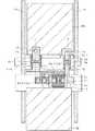
この光センサ内蔵表示装置40のTFTアレイ基板40aは、図1および図2の様に、透明基板1上に、微結晶シリコンTFTで構成された第1の光電変換用TFT20と、非晶質シリコンTFTで構成された第2の光電変換用TFT21と、周辺回路(光センサ信号読出用TFT22や走査回路等)と、画素駆動用TFT12とを備えて構成される。第1および第2の光電変換用TFT20,21により上記の光センサが構成されている。 As shown in FIG. 1 and FIG. 2, the
より詳細には、ガラス基板等の透明基板1上に、金属膜から成るゲート電極2a(2a−1,2a−2),2bがパターン形成されている。透明基板1の上面全面には、ゲート電極2a,2bを被覆する様に、シリコン窒化膜またはシリコン窒化膜から成るゲート絶縁膜3が形成されている。 More specifically,
各ゲート電極2a−1,2a−2,2b上にはそれぞれ、絶縁膜3を介して、微結晶シリコン膜から成るTFT用チャネル層4a,4b,4cが形成されている。各チャネル層4a,4b,4cの上面の両側部分上には、リンを不純物として添加したn型微結晶シリコン膜から成るオーミックコンタクト層5が形成されている。 On each
各チャネル層4a,4b,4cの上面の両側のオーミックコンタクト層5のうち、一方のオーミックコンタクト層5上には、ソース電極7a,7c,7eが形成されており、他方のオーミックコンタクト層5上には、ドレイン電極7b,7d,7fが形成されている。ソース電極7bとドレイン電極7cは、互いに接続されている。 Of the
また透明基板1の上面全面には、絶縁膜3、ソース電極7a,7c,7e、ドレイン電極7b,7d,7fおよびチャネル層4a,4b,4cを被覆する様に、透明な絶縁部材から成る保護膜8が形成されている。 Further, the entire upper surface of the
保護膜8の中には、一部のチャネル層4b上に間隔を空けて対向配置する様に、非晶質シリコン膜からなるチャネル層11が形成されている。このチャネル層11は、その下面の両側にそれぞれコンタクト部c1,c2を有しており、その一方のコンタクト部c1を介してソース電極7cおよびその下層のオーミック層5に接続され、その他方のコンタクト部c2を介してドレイン電極7dおよびその下層のオーミックコンタクト層5に接続されている。 A
保護膜8上には、透明電極から成る画素電極9a(9a−1,9a−2),9bがパターン形成されている。画素電極9aの部分9a−1(以後、画素電極9a−1と呼ぶ)は、チャネル層11上に保護膜8を介して対向配置している。画素電極9aの部分9a−2(以後、画素電極9a−2と呼ぶ)は、その下面にコンタクト部c4,c5を有し、それら各コンタクト部c4,c5を介してドレイン電極7d,ゲート電極2bに接続されている。画素電極9bは、その下面にコンタクト部c3を有し、そのコンタクト部c3を介してドレイン電極7fに接続されている。 On the
また透明基板1上には、データ配線14(図1,図2)、光センサ信号読出配線18、ゲート配線15(図4)およびコモン配線16が形成されている。データ配線14には、ソース電極7eが接続されている。光センサ信号読出配線18には、ソース電極7aが接続されている。ゲート配線15には、ゲート電極2a−1,2a−2が接続されている。コモン配線16には、ドレイン電極7dが接続されている。 On the
またコモン配線16とドレイン電極7fとの間には、画素電荷保持容量13(図4)が形成されており、コモン電極16とソース電極9cとの間には、光センサ用電荷保存容量24(図4参照)が形成されており、ゲート電極7fには、画素部液晶容量25(図4)が形成されている。 A pixel charge storage capacitor 13 (FIG. 4) is formed between the
この構成により、ゲート電極2a−1,ソース電極7a,ドレイン電極7bおよびチャネル層4aにより微結晶シリコンTFTが構成され、その微結晶シリコンTFTにより光センサ信号読出用TFT22が構成されている。またゲート電極2a−2,ソース電極7e,ドレイン電極7fおよびチャネル層4cにより微結晶シリコンTFTが構成され、その微結晶シリコンTFTにより画素駆動用TFT12が構成されている。 With this configuration, the
またゲート電極2b,ソース電極7c,ドレイン電極7dおよびチャネル層4bにより微結晶シリコンTFTが構成され、その微結晶シリコンTFTにより、チャネル層4bによる近赤外光の吸収によりオン駆動する第1の光電変換用TFT20が構成されている。また画素電極(ゲート電極)9a−1,ソース電極7c,ドレイン電極7dおよびチャネル層11により非晶質シリコンTFTが構成され、その非晶質シリコンTFTにより、チャネル層11による可視光の吸収によりオン駆動する第2の光電変換用TFT21が構成されている。 The
また第1および第2の光電変換用TFT20,21は、それらのドレイン電極7d同士、それらのソース電極7c同士、それらのゲート電極2b,9a−1同士が相互接続されて、互いに並列接続されている。 The first and second
また微結晶シリコンTFTで構成された第1の光電変換用TFT20が基板1上に配置され、その第1の光電変換用TFT20のチャネル層4bの上方に、非晶質シリコンTFTで構成された第2の光電変換用TFT21が配置されている。 A first
また光センサ信号読出用TFT22のドレイン電極7bと、第1および第2の光電変換用TFT20,21のソース電極7cとが接続されることで、光センサ信号読出用TFT22が第1および第2の光電変換用TFT20,21に直列接続されている。 Further, the
尚、透明基板1上の周縁には、光センサ信号読出用TFT32等と同様の構造の微結晶シリコンTFTで構成された垂直走査回路35(図4)、および第1および第2の光電変換用TFT20,21と同様の構造の微結晶シリコンTFTおよび非晶質シリコンTFTで構成された光センサ回路37が配設されている。 A vertical scanning circuit 35 (FIG. 4) composed of microcrystalline silicon TFTs having the same structure as the photosensor signal readout TFT 32 and the like and the first and second photoelectric conversion circuits are provided on the periphery of the
尚、この様に構成されたTFTアレイ基板40aの前面(TFT側の面)上には、液晶パネル部が形成される。 A liquid crystal panel portion is formed on the front surface (TFT side surface) of the
この光センサ内蔵表示装置40は、図5の様に、上記のTFTアレイ基板40aと、TFTアレイ基板40aの前面(TFT側の面)側に配置されたカラーフィルター基板40bと、TFTアレイ基板40aの裏面側に配置された導光板40cと、導光板40cの一方の端面に対向配置されたバックライト光源40dと、導光板4cの他方の端面に対向配置された補助光源40eとを備えて構成される。バックライト光源40dは、TFTアレイ基板40aの液晶パネル部を照らし出すためのバックライト光(可視光)を発光する。補助光源40eは、第1の光電変換用TFT20のチャネル層4bが吸収可能な波長帯域(例えば約700nm〜900nm)の近赤外光(補助光)を発光する。 As shown in FIG. 5, the optical sensor built-in
この構成により、バックライト光源40dからのバックライト光は、導光板40d内を導光して導光板40dの前面から射出して、TFTアレイ基板40aおよびカラーフィルター基板40bを透過して照らし出さす。 With this configuration, the backlight light from the
また補助光源40eからの近赤外光は、導光板40d内を導光して導光板40dの前面から射出して、TFTアレイ基板40aのゲート電極2a,2b間を通過してTFTアレイ基板40aおよびカラーフィルター基板40bを透過して、カラーフィルター基板40bの前面側に射出する。 The near-infrared light from the auxiliary
そしてその照らし出されたバックライト光またはその射出された近赤外光は、カラーフィルター基板40bの前面を指押しする人の当該指55で反射して、再びカラーフィルター基板40bおよびTFTアレイ基板40aを透過して、TFTアレイ基板40a内の第1または第2の光電変換用TFT20,21のチャネル層4b,11に入射して吸収される。この反射光の吸収により、その反射光を吸収した第1または第2の光電変換用TFT20,21がオン駆動し、このオン駆動により、カラーフィルター基板40bの前面への当該指押しが検知される。尚この場合、強いバックライト光を用いる場合は、補助光源40eを消灯しても良い。これにより消費電力を低減できる。 The illuminated backlight light or the emitted near-infrared light is reflected by the
尚、図6の様に、補助光源40eをカラーフィルタ基板40eの前面側に配置し、前面側からカラーフィルタ基板40bおよびTFTアレイ基板40aを透過して第1および第2の光センサ用TFT20,21のチャネル層4b,11に入射する、補助光源40eからの近赤外光および太陽光等の外光が指55で遮光されか否かを、第1および第2の光センサ用TFT20,21で検出する(即ち指55の指影を検出する)ことで、カラーフィルタ基板40bの前面への指押しを検出しても良い。尚この場合、外光が有る場合は、補助光源40eを省略し、その外光を補助光の代わりに利用しても良い。 As shown in FIG. 6, the auxiliary
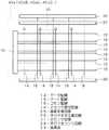
<TFTアレイ基板40aの等価回路図>
図3は、TFTアレイ基板40aの等価回路およびその周囲回路(走査回路など)を示した図であり、図4は、図3の画素部分39の拡大図である。<Equivalent circuit diagram of
FIG. 3 is a diagram showing an equivalent circuit of the
このTFTアレイ基板40aの等価回路は、図3の様に、縦横に間隔を空けて配置されたデータ配線14、ゲート配線15、コモン配線16および光センサ信号配線18と、垂直走査回路35と、光センサ回路37とを備えている。尚、図3中の符号36は、外付けの水平走査回路であり、符号38は、外付けの光センサ回路である。 As shown in FIG. 3, the equivalent circuit of the
各配線14,15,16,18で区画された各領域39が画素部である。TFTアレイ基板40aの各画素部39には、図4の様に、第1および第2の光電変換用TFT20,21と、光センサ信号読出用TFT22と、画素駆動用TFT12と、画素電荷保持容量13と、光センサ用電荷保持容量24と、画素部液晶容量25とが備えられている。 Each
前述の通り、第1の光電変換用TFT20、光センサ信号読出用TFT22および画素駆動用TFT12はそれぞれ、微結晶シリコンTFTで構成され、第2の光電変換用TFT21は、非晶質シリコンTFTで構成されている。 As described above, the first
画素駆動用TFT12は、そのゲート電極2a−2がゲート配線15に接続され、そのソース電極7eがデータ配線14に接続され、そのドレイン電極7fが画素電荷保持容量13を介してコモン配線16に接続されて配設されている。また画素駆動用TFT12のドレイン電極7fには、画素部液晶容量25が接続されている。 The
第1および第2の光電変換用TFT20,21は、それらのドレイン電極7dが相互接続されてコモン電極16に接続され、それらのソース電極7cが相互接続されて光センサ用電荷保持容量24を介してコモン配線16に接続され、それらのゲート電極2b,9a−1およびそれらのドレイン電極7dが相互接続されてコモン配線16に接続されて配設されている。 In the first and second
光センサ信号読出用TFT22は、そのゲート電極2a−1がゲート配線15に接続され、そのソース電極7aが光センサ信号配線18に接続され、そのドレイン電極7bが、第1および第2の光電変換用TFT20,21のドレイン電極7cに接続されて配設されている。 The photosensor
画素電荷保持容量13は、画素電極9b(図2)に蓄積された電荷を保持し、画素駆動用TFT12のゲート電極2a−2に印加される電圧の低下を防止する目的で設けられている。 The pixel
光センサ回路37は、マルチプレクサ回路等からなる回路であり、光電変換用TFT20,21と同様の構造の微結晶シリコンTFTおよび非晶質シリコンTFTで構成されている。尚、光センサ回路38は、電荷や電流を検出する検出回路等からなる回路である。光センサ回路37,38により、各光センサ信号配線18を通じて各画素部39の光電変換用TFT20,21から出力される光センサ信号が検知される。 The
垂直走査回路35は、光センサ信号読出用TFT32等と同様の構造の微結晶シリコンTFTで構成されている。この垂直走査回路35は、例えば、各ゲート電極15に対して上から順に1つずつ電圧を印加して、各TFT12,22のゲート電極2a−2,2a−1に駆動電圧を印加する。また水平走査回路36は、例えば、画像信号に基づき各データ配線14を選択的に低電位源に接続して、画素駆動用TFT12のソース電極7eを低電位源に接続する。 The
この構成により、各画素部39の画素駆動用TFT12は、そのゲート電極2a−2に駆動電圧が垂直走査回路35により印加されると共に、そのソース電極7eが水平走査回路36により低電位源に接続されると、オン駆動する。 With this configuration, the driving voltage is applied to the
また各画素部39の第1の光電変換用TFT20は、そのチャネル層4bに近赤外光が入射すると、オン駆動する。また各画素部39の第2の光電変換用TFT21は、そのチャネル層11に可視光が入射すると、オン駆動する。 The first
そして垂直走査回路35により、光センサ信号読出用TFT22のゲート電極2a−1に駆動電圧が印加されて光センサ信号読出用TFT22がオン駆動した状態で、第1および第2の光電変換用TFT20,21の少なくとも一方がオン駆動すると、光センサ信号配線18からの電流が、光センサ信号として、当該オン駆動した光電変換用TFT20,21および光センサ信号読出用TFT22を通じてコモン配線16に流れる。そして、この光センサ信号が光センサ回路37,38により検知されることで、カラーフィルター基板40bの前面への指押しが検出される。 Then, the
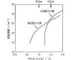
<第1の光電変換用TFT20のチャネル層4bの光吸収特性の最適化>
図7は、微結晶シリコン膜および非晶質シリコン膜の各々の波長と吸収係数との関係を示したグラフである。図8は、微結晶シリコン膜および非晶質シリコン膜の各々の波長と光電変換効率(量子化効率)との関係を示したグラフである。<Optimization of light absorption characteristics of
FIG. 7 is a graph showing the relationship between the wavelength and the absorption coefficient of each of the microcrystalline silicon film and the amorphous silicon film. FIG. 8 is a graph showing the relationship between the wavelength of each of the microcrystalline silicon film and the amorphous silicon film and the photoelectric conversion efficiency (quantization efficiency).
図7および図8から、微結晶シリコン膜は、非晶質シリコン膜とは異なり、補助光源40eから発光される700nm〜850nmの波長帯域の近赤外光にも十分な感度を有している事が分かる。 7 and 8, unlike the amorphous silicon film, the microcrystalline silicon film has sufficient sensitivity to near-infrared light in the wavelength band of 700 nm to 850 nm emitted from the auxiliary
ここで留意すべき点は、一般に、微結晶シリコン膜は、その結晶サイズが大きくなる程にバンドギャップは小さくなる反面、その膜厚が厚くなる程に吸収係数が小さくなる傾向があると言うことである。この観点から、700nm〜850nmの波長帯域の近赤外光に対する吸収係数が十分な値となる微結晶シリコン膜(即ち、光電変換用TFT20のチャネル層4bに適した微結晶シリコン膜)としては、結晶サイズが5nm〜50nm(換言すれば、その結晶粒径が100nm以下)であり、且つ光学的バンドギャップが、図3を参照して、上記の波長帯域内の最小エネルギに相当する約1.4eVの微結晶シリコン膜である事が分かる。 It should be noted that, in general, the microcrystalline silicon film has a tendency that the absorption coefficient tends to decrease as the film thickness increases while the band gap decreases as the crystal size increases. It is. From this point of view, as a microcrystalline silicon film (that is, a microcrystalline silicon film suitable for the
更に、結晶シリコン相と非晶質相とのラマン分光の信号強度比(Ic/Ia)が3〜10程度、換言すれば、微結晶シリコン膜の非晶質領域と結晶領域との比率が1/10〜1/5程度の微結晶シリコン膜であることが望ましい。そして、光学的バンドギャップおよびラマン分光の信号強度比を、光センサとして要求される分光感度特性に合わせて調整することが望ましい。 Further, the signal intensity ratio (Ic / Ia) of Raman spectroscopy between the crystalline silicon phase and the amorphous phase is about 3 to 10, in other words, the ratio of the amorphous region to the crystalline region of the microcrystalline silicon film is 1. A microcrystalline silicon film of about / 10 to 1/5 is desirable. Then, it is desirable to adjust the signal intensity ratio of the optical band gap and Raman spectroscopy in accordance with the spectral sensitivity characteristics required for the optical sensor.
この様な微結晶シリコン膜は、例えば、平行平板型プラズマCVD装置において、H2ガスとSiH4ガスとの流量比を10以上とし、プラズマの放電条件である圧力や投入電力、あるいは基板温度や電極間距離を調整することで、作成できる。特に、H2ガスとSiH4ガスとの流量比120、圧力800Pa、基板温度300℃に調整することで、所望の微結晶シリコン膜を作成できる。または、H2ガスの代わりにArガスや、SiH4の代わりにSiF4等のガスを用いても良い。更に、平行平板型プラズマCVD装置の代わりに誘導結合型プラズマCVD装置を用いても、良好な微結晶シリコン膜を作成できる。Such a microcrystalline silicon film has a flow rate ratio of H2 gas to SiH4 gas of 10 or more in a parallel plate type plasma CVD apparatus, for example, pressure or input power, plasma temperature, substrate temperature, It can be created by adjusting the distance between the electrodes. In particular, a desired microcrystalline silicon film can be formed by adjusting the flow ratio of H2 gas and SiH4 gas to 120, the pressure of 800 Pa, and the substrate temperature of 300 ° C. Alternatively, Ar gas may be used instead of H2 gas, and gas such as SiF4 may be used instead of SiH4 . Furthermore, even if an inductively coupled plasma CVD apparatus is used instead of the parallel plate type plasma CVD apparatus, a good microcrystalline silicon film can be formed.
尚、リンを不純物として添加した微結晶シリコン膜(オーミックコンタクト層)5の代わりに非晶質シリコン膜を用いても、同等の効果が得られる。 Even if an amorphous silicon film is used instead of the microcrystalline silicon film (ohmic contact layer) 5 doped with phosphorus as an impurity, the same effect can be obtained.
以上の様に構成された光センサ内蔵表示装置40によれば、TFTアレイ基板40aの各画素部に、微結晶シリコンTFT(即ち近赤外光の入射でオン駆動するTFT)で構成された第1の光電変換用TFT20と、非晶質シリコンTFT(即ち可視光の入射でオン駆動するTFT)で構成され、第1の光電変換用TFT20と並列接続された第2の光電変換用TFT21とを備えるので、可視光だけでなく近赤外光も検出できる。これにより、バックライト光(可視光)に近赤外光を重ねることで、バックライト光の輝度調整(即ち表示画面の輝度調整)に影響を与えずに光センサの検出精度を向上できる。 According to the
また可視光だけでなく近赤外光も検出できるので、暗い場所では、人に視認されない近赤外光により指押しを検出でき、他方、明るい場所では、近赤外を使用しないで、外光やバックライト光により指押しを検出できるため、消費電力の削減も可能になる。 Since not only visible light but also near-infrared light can be detected, finger pressing can be detected by near-infrared light that is not visible to humans in dark places, while outside light can be detected without using near-infrared light in bright places. Since the finger press can be detected by the backlight and the power, the power consumption can be reduced.
また微結晶シリコンTFTは、その移動度が非晶質シリコンTFTの移動度よりも3〜5倍高いので、スイッチング特性に優れている。従って、上記の様に第1および第2の光電変換用TFT20,21を同一基板上に備えることで、可視光から紫外光までの広い感度を持つと共にスイッチング特性に優れた光センサをTFTアレイ基板40a上に形成できる。このため、高性能な光センサを搭載したTFTアレイ基板40aを実現できる。 Microcrystalline silicon TFTs have excellent switching characteristics because their mobility is 3 to 5 times higher than that of amorphous silicon TFTs. Therefore, by providing the first and second
光センサ信号読出用TFT22が微結晶シリコンTFTで構成されるので、光センサ信号読出用TFT22をTFTアレイ基板40aの各画素部に備えることができ、これにより回路規模の増大を防止でき、且つ実装工程での歩留を増加できて製造コストを低減できる。 Since the optical sensor
第1の光電変換用TFT20は、透明基板1上にゲート電極2bが形成され、その上にゲート絶縁膜3を介してチャネル層4bが形成されたボトムゲート構造に構成されるので、従来のトップゲート構造と異なり、外光がTFTアレイ基板40a上のTFTの電極で反射する事を防止でき、表示品質の低下を防止できる。 The first
第2の光電変換用TFT21は、そのチャネル層11が第1の光電変換用TFT20のチャネル層4b上に絶縁層(ここでは保護膜8)を介して形成され、そのゲート電極9a−1がそのチャネル層11上に絶縁層(ここでは保護膜8)を介して形成されるので、即ち第2の光電変換用TFT21は第1の光電変換用TFT20の上方に形成されるので、素子の配置面積を低減でき、画素の開口率の減少を防止できる。 The
また第2の光電変換用TFT21のチャネル層(非晶質シリコン層)11は、第1の光電変換用TFT20のゲート絶縁膜3の上方に形成されるので、第1の光電変換用TFT20の製造工程の影響を受ける事を防止できる。 Further, since the channel layer (amorphous silicon layer) 11 of the second
また画素電極9a−1,9a−1,2bは透明電極により形成されるので、画素電極9a−1,9a−1,2bにより第1および第2の光電変換用TFT20,21のチャネル層4b,11への入射光が遮光される事を防止できる。 Since the
実施の形態2.
この実施の形態では、図1および図2に基づき、実施の形態1のTFTアレイ基板40aの製造方法を説明する。
In the present embodiment, a method for manufacturing the
先ず、透明基板1上にスパッタ法等で金属膜を形成し、その金属膜を写真製版工程によりパターニングして、ゲート電極2a,2b、ゲート配線15(図3)およびコモン配線16(図3)をパターン形成する。 First, a metal film is formed on the
次に、透明基板1の上面全面に、プラズマCVD装置を用いて、上記のゲート電極2a,2b、ゲート配線15およびコモン配線16を被覆する様に、ゲート絶縁膜3に成るシリコン窒化膜を200nm〜500nmの範囲内の厚みで形成し、更にその上に、チャネル層4a,4b,4cに成る微結晶シリコン膜を100nm〜500nmの範囲内の厚みで形成し、更にその上に、オーミックコンタクト層5に成る、リンを不純物として添加した微結晶シリコン膜(以後、リンドープ微結晶シリコン膜と呼ぶ)を30nm〜100nmの範囲内の厚みで形成する。 Next, a silicon nitride film serving as the
そして上記の形成した微結晶シリコン膜およびリンドープ微結晶シリコン膜をパターニングして、チャネル層4a,4b,4cをパターン形成する。尚、この状態では、上記のリンドープ微結晶シリコン膜は、各チャネル層4a,4b,4cの上面全面に形成されたままである。 Then, the above-formed microcrystalline silicon film and phosphorus-doped microcrystalline silicon film are patterned to form
そして透明基板1の上面全面に、ゲート絶縁膜3、チャネル層4a,4b,4cおよび上記のリンドープ微結晶シリコン膜を被覆する様に、スパッタ法等で金属膜を形成し、その金属膜をパターニングして、ソース電極7a,7c,7d、ドレイン電極7b,7d,7e、データ配線14(図3)および光センサ信号配線18(図3)をパターン形成する。 Then, a metal film is formed on the entire upper surface of the
そして上記のリンドープ微結晶シリコン膜を、各チャネル層4a,4b,4cの上面の両側部分上の部分だけを残してエッチング除去して(バックチャネルエッチ)、オーミックコンタクト層5をパターン形成する。 Then, the above-mentioned phosphorus-doped microcrystalline silicon film is removed by etching (back channel etch) leaving only portions on both side portions of the upper surfaces of the
そして透明基板1の上面全面に、ゲート絶縁膜3、チャネル層4a,4b,4cおよびオーミックコンタクト層5を被覆する様に、シリコン窒化膜またはシリコン酸化膜により、先ず保護膜8の下半層だけを形成する。 Then, only the lower half layer of the
そして保護膜8の前記下半層の上面に、オーミックコンタクト層5に達する様にコンタクトホールhaを形成する。そして保護膜8の前記下半層の上面全面に、コンタクトホールha内に充填する様に、チャネル層11に成る非晶質シリコン膜を形成する。そしてその非晶質シリコン膜を、チャネル層4b上の部分だけを残す様にパターニングして、チャネル層11をパターン形成する。 A contact hole ha is formed on the upper surface of the lower half layer of the
尚、コンタクトホールhaの形成後、コンタクトホールhaの内面に対して、リンまたはホスフィンによるプラズマ処理を行うことで、各コンタクト部c1,c2と各電極7c,7dとのコンタクトを改善できる。 Incidentally, after the contact hole ha is formed, the contact between the contact portions c1 and c2 and the
そして保護膜8の前記下半層の上面全面に、チャネル層11を被覆する様に、シリコン窒化膜またはシリコン酸化膜により保護膜8の上半層を形成して、保護膜8を完成させる。 Then, the upper half layer of the
そして保護膜8の上面に、ドレイン電極7d,7fまたはゲート電極2bに達する様に各コンタクトホールhbを形成する。そして保護膜8の上面全面に、コンタクトホールhb内に充填する様に、透明電極から成る画素電極9a(9a−1,9a−2),9bをパターン形成する。この様にしてTFTアレイ基板40aが製造される。 Then, each contact hole hb is formed on the upper surface of the
実施の形態3.
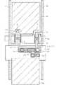
実施の形態1では、第2の光電変換用TFT21は、そのチャネル層11が第1の光電変換用TFT20のチャネル層4b上に保護膜8を介して形成され、そのゲート電極9a−1がそのチャネル層11上に保護膜8を介して(即ち保護膜8の上面上に)形成される様に設けられた。この構造では、第2の光電変換用TFT21のチャネル層11は、保護膜8を介して第1の光電変換用TFT20のチャネル層4bと対向するので、第2の光電変換用TFT21のバックゲートが制御し難くなる。
In
そこで、この実施の形態では、図9および図10の様に、第2の光電変換用TFT21は、そのゲート電極9a−1が第1の光電変換用TFT20のチャネル層4b上に保護膜8を介して形成され、そのチャネル層11がそのゲート電極9a−1に保護膜8を介して(即ち保護膜8の上面上に)形成される様に設けられている。これにより、第2の光電変換用TFT21のバックゲート制御が可能になり、オフ電流が小さく、良好な光電変換特性を得られる。 Therefore, in this embodiment, as shown in FIGS. 9 and 10, the second
尚この実施の形態では、画素電極9a−2,9bは、ゲート電極(画素電極)9a−1と同一工程で形成されているので、ゲート電極9a−1と共に保護膜8内に形成されている。尚、他の部分は、実施の形態1と同様である。 In this embodiment, since the
実施の形態4.
この実施の形態では、図9および図10に基づき、実施の形態3の場合のTFTアレイ基板40aBの製造方法を説明する。
In the present embodiment, a method for manufacturing the TFT array substrate 40aB in the case of the third embodiment will be described with reference to FIGS.
保護膜8の下半層を形成するまでは、実施の形態2の製造方法と同じである。そしてその保護膜8の前記下半層の上面に、ソース電極7d,7fまたはゲート電極2bに到達する様に各コンタクトホールhbを形成する。そして保護膜8の前記下半層の上面上に、それら各コンタクトホールhbを充填する様に、透明電極から成る画素電極9a(9a−1,9a−2),9bをパターン形成する。そして保護膜8の前記下半層の上面全面に、画素電極9a,9bを被覆する様に保護膜8の上半層を形成して、保護膜8を完成させる。そして保護膜8の上面に、ソース電極7c,ドレイン電極7dに達する各コンタクトホールhaを形成する。そして保護膜8の上面に、各コンタクトホールhaを充填する様に、非晶質シリコン膜から成るチャネル層5をパターン形成する。この様にしてTFTアレイ基板40aAを製造する。 The manufacturing method of the second embodiment is the same until the lower half layer of the
実施の形態5.
実施の形態1,3では、第1の光電変換用TFT20と、第2の光電変換用TFT21とを互いに並列接続したが、この実施の形態では、第1の光電変換用TFT20と、第2の光電変換用TFT21とを互いに直列接続する。以下、図11〜図13に基づき、この実施の形態の場合のTFTアレイ基板40aCについて説明する。
In the first and third embodiments, the first
<全体構成>
この実施の形態に係る光センサ内蔵表示装置40のTFTアレイ基板40aCは、図11および図12の様に構成されている。即ち、ガラス基板等の透明基板1上に、金属膜から成るゲート電極2a(2a−1,2a−2),2bがパターン形成されている。透明基板1の上面全面には、ゲート電極2a,2bを被覆する様に、シリコン窒化膜またはシリコン窒化膜から成るゲート絶縁膜3が形成されている。<Overall configuration>
The TFT array substrate 40aC of the
また各ゲート電極2a−1,2a−2,2b上にはそれぞれ、絶縁膜3を介して、微結晶シリコン膜から成るチャネル層4a,4b,4cが形成されている。各チャネル層4a,4b,4cの上面の両側部分上には、リンを不純物として添加したn型微結晶シリコン膜から成るオーミックコンタクト層5が形成されている。 On the
また各チャネル層4a,4b,4cの上面の両側のオーミックコンタクト層5のうち、一方のオーミックコンタクト層5上には、ソース電極7a,7d,7eが形成されており、他方のオーミックコンタクト層5上には、ドレイン電極7b,7c,7fが形成されている。
また透明基板1の上面全面には、絶縁膜3、ソース電極7a,7d,7e,ドレイン電極7b,7c,7fおよびチャネル層4a,4b,4cを被覆する様に、透明な絶縁部材から成る保護膜8が形成されている。 Further, the entire upper surface of the
また保護膜8の中には、透明電極から成る画素電極9b,9c,9d,9eが形成されている。画素電極9bは、その下面にコンタクト部c3が形成されており、そのコンタクト部c3を介してドレイン電極7fに接続されている。画素電極9cは、その下面にコンタクト部c12が形成されており、そのコンタクト部c12を介してドレイン電極7bに接続されている。画素電極9eは、その下面にコンタクト部c8,c9が形成されており、その一方のコンタクト部c8を介してゲート電極2bに接続されており、その他方のコンタクト部c9を介してドレイン電極7cに接続されている。画素電極9dは、チャネル層4b上に保護膜8を介して形成されている。また画素電極9dは、その下面の一方側にコンタクト部c7が形成されており、そのコンタクト部c7を介してソース電極7dに接続されている。 In the
また保護膜8の上面上には、非晶質シリコン膜からなるチャネル層11が形成されている。チャネル層11の部分11a(以後、チャネル層11aと呼ぶ)は、画素電極9d上に保護膜8を介して形成されている。チャネル層11の部分11b(以後、チャネル層11bと呼ぶ)は、画素電極9c上に保護膜8を介して形成されている。チャネル層11aは、その下面にコンタクト部c11が形成されており、そのコンタクト部c11を介して画素電極9dに接続されている。またチャネル層11bは、その下面にコンタクト部c12が形成されており、そのコンタクト部c12を介して画素電極9cに接続されている。 A
また透明基板1上には、データ配線14(図13)、光センサ信号読出配線18(図13)、ゲート配線15(図13)およびコモン配線16(図13)が形成されている。データ配線14には、ソース電極7eが接続されている。光センサ信号読出配線18には、ソース電極7aが接続されている。ゲート配線15には、ゲート電極2a−1,2a−2が接続されている。コモン配線16には、ゲート電極2bおよびドレイン電極7cが接続されている。 On the
またコモン配線16とドレイン電極7fとの間には、画素電荷保持容量13(図13)が形成されており、コモン電極16とソース電極9cとの間には、光センサ用電荷保存容量24(図13)が形成されている。 A pixel charge storage capacitor 13 (FIG. 13) is formed between the
この構成により、ゲート電極2a−2,ソース電極7e,ドレイン電極7fおよびチャネル層4cにより微結晶シリコンTFTが構成され、その微結晶シリコンTFTにより画素駆動用TFT12が構成されている。この画素駆動用TFT12は、図13の様に、そのゲート電極2a−2がゲート電極15に接続され、そのソース電極7eがデータ配線14に接続され、そのドレイン電極7fが画素電荷保存容量13を介してコモン配線16に接続されて配設されている。 With this configuration, the
またゲート電極2a−1,ソース電極7a,ドレイン電極7bおよびチャネル層4aにより微結晶シリコンTFTが構成され、その微結晶シリコンTFTにより光センサ信号読出用TFT22が構成されている。この光センサ信号読出用TFT22は、図13の様に、そのゲート電極2a−1がゲート電極15に接続され、そのソース電極7aが光センサ信号配線18に接続され、そのドレイン電極7bが第2の光電変換用TFT21のソース電極9cに接続されて配設されている。 The
またゲート電極2b,ドレイン電極7c,ソース電極7dおよびチャネル層4bにより微結晶シリコンTFTが構成され、その微結晶シリコンTFTにより第1の光電変換用TFT20が構成されている。この第1の光電変換用TFT20は、図13の様に、そのゲート電極2bおよびそのドレイン電極7cがコモン配線16に接続され、そのソース電極7dが第2の光電変換用TFT21のドレイン電極9d−2に接続されて配設されている。 The
またゲート電極(画素電極9dの部分)9d−1、ドレイン電極(画素電極9dの部分)9d−2,ソース電極(画素電極)9cおよびチャネル層11(11aおよび11b)により非晶質シリコンTFTが構成され、その非晶質シリコンTFTにより第2の光電変換用TFT21が構成されている。この第2の光電変換用TFT21は、図13の様に、そのゲート電極9d−1およびそのドレイン電極9d−2が第1の光電変換用TFT20のソース電極7dに接続され、そのソース電極9cが光センサ信号読出用TFT22のドレイン電極7bに接続されると共に光センサ用電荷保存容量24を介してコモン配線16に接続されて配設されている。 The gate electrode (
この様に、この実施の形態では、第1および第2の光電変換用TFT20,21は、互いに直列接続されて配設されている。 Thus, in this embodiment, the first and second
この構成により、この実施の形態では、直走査回路35(図3)により、光センサ信号読出用TFT22のゲート電極2a−1に駆動電圧が印加されて光センサ信号読出用TFT22がオン駆動した状態で、チャネル層4bに近赤外光が入射して第1の光電変換用TFT20がオン駆動すると共に、チャネル層11に可視光が入射して第2の光電変換用TFT21がオン駆動すると、例えば、光センサ信号配線18からの電流が、光センサ信号として、オン駆動した光電変換用TFT20,21を通じてコモン配線16に流れる。 With this configuration, in this embodiment, the direct scanning circuit 35 (FIG. 3) applies a driving voltage to the
この様に、第1の光電変換用TFT(微結晶シリコンTFT)20と、第2の光電変換用TFT(非晶質シリコンTFT)21とを直列接続することで、太陽光の様な可視光と近赤外光とを含む光が入射した場合のみ、その光が光センサにより検出される。 In this way, the first photoelectric conversion TFT (microcrystalline silicon TFT) 20 and the second photoelectric conversion TFT (amorphous silicon TFT) 21 are connected in series, so that visible light such as sunlight is visible. Only when light including near infrared light is incident, the light is detected by the optical sensor.
これにより、例えばタッチセンサとして、図6の様に、太陽光を利用して指押しの際の指影を第1および第2の光センサ用TFT20,21で検出して、カラーフィルタ基板40bの前面への指押しを検出する場合、光センサを、可視光だけの入射や近赤外光だけの入射には反応させず、太陽光(可視光と近赤外光とを含む光)の入射だけに反応させる事ができ、バックライト光(可視光)の表示装置内部での反射光等の太陽光以外の光による誤動作を防止できる。 Thereby, as shown in FIG. 6, for example, as shown in FIG. 6, the finger shadow when the finger is pressed is detected by the first and
また図5の様にバックライト光(可視光)と補助光(近赤外光)とを重ねてカラーフィルタ基板40bを照らし出す場合、指押しの際の指55で反射される反射光は、バックライト光と補助光とを含む光である。即ちバックライト光だけの反射光や補助光だけの反射光は、指押しの際の指55での反射によるものではない。そのため、上記の様に、可視光と近赤外光とが同時に入射する場合のみ、その光が検出される様にすることで、図5の場合においても、カラーフィルタ基板40bの前面の指押しだけを正しく検出でき、誤動作を防止できる。 Further, as shown in FIG. 5, when the backlight (visible light) and auxiliary light (near infrared light) are overlapped to illuminate the
実施の形態6.
この実施の形態に係る光センサ内蔵表示装置は、図14の様に、実施の形態1,3における第1および第2の光電変換用TFT20,21を互いに並列接続した場合(図4)の画素部39(39A)と、実施の形態5における第1および第2の光電変換用TFT20,21を互いに直列接続した場合(図12)の画素部39(39B)とを縦横に交互に配置して、TFTアレイ基板40aDを構成したものある。尚、上記の様に交互にしなくても、TFTアレイ基板40aDの各画像部のうち、所定の画素部を画素部39Aとし、他の画素部を画素部29Bとしても良い。Embodiment 6 FIG.
As shown in FIG. 14, the display device with a built-in photosensor according to this embodiment has a pixel when the first and second
この様に並列接続の光電変換用TFT20,21と直列接続の光電変換用TFT20,21との両方を配置することで、実施の形態1,3,5の効果を得る。即ち外光(太陽光の様な可視光と近赤外光とを含む光)が有る場合は、直列接続の光電変換用TFT20,21により、当該外光以外の光(バックライト光など)の反射光の影響を受けずに高感度で指影(従って指押し)を検出でき、他方、外光が無い場合には、並列接続の光電変換用TFT20,21により、高感度にバックライト光または補助光(近赤外光)の指での反射光を検出できる(従って指押しを検出できる)。 The effects of the first, third, and fifth embodiments can be obtained by arranging both the parallel-connected
また、一般にタッチセンサに要求される分可能は1mm程度であるが、この様に並列接続の光電変換用TFTと直列接続の光電変換用TFTとを各画素毎に交互に配設しても、十分な分解能が得られる。 In general, the required amount of the touch sensor is about 1 mm. In this way, even if the parallel-connected photoelectric conversion TFTs and the series-connected photoelectric conversion TFTs are alternately arranged for each pixel, Sufficient resolution can be obtained.
1 透明基板、2a,2a−1,2a−2,2b ゲート電極、3 ゲート絶縁膜、4a,4b,4c チャネル層(微結晶シリコン膜)、5 オーミックコンタクト層、7a〜7f ソース電極またはドレイン電極、8 保護膜、9a〜9e,9d−1,9d−2 画素電極、11a,11a−1,11a−2,11b チャネル層(非晶質シリコン膜)、12 画素駆動用TFT、13 画素電荷保持容量、14 データ配線、15 ゲート配線、16 コモン配線、18 光センサ信号配線、20 第1の光電変換用TFT、21 第2の光電変換用TFT、24 光センサ用電荷保持容量、25 画素部液晶容量、35 垂直走査回路、36 外付け水平走査回路、37 光センサ回路、38 外付け光センサ回路、39,39A,39B 画素部、40 光センサ内蔵表示装置、40a,40aB,40aC,40aD TFTアレイ基板、40b カラーフィルター基板、40c 導光板、40d バックライト光源、40e 補助光源、c1〜c5,c7〜c9,c11,c12 コンタクト部、ha,hb コンタクトホール。 DESCRIPTION OF
Claims (13)
Translated fromJapanese微結晶シリコンTFTで構成された画素駆動用TFTと、
微結晶シリコンTFTで構成された第1の光電変換用TFTと、
非晶質シリコンTFTで構成され、前記第1の光電変換用TFTと並列接続された第2の光電変換用TFTと、
を備えることを特徴とする光センサ内蔵表示装置。In each pixel portion of the TFT (TFT: thin film transistor) array substrate,
A pixel driving TFT composed of a microcrystalline silicon TFT;
A first photoelectric conversion TFT composed of a microcrystalline silicon TFT;
A second photoelectric conversion TFT composed of an amorphous silicon TFT and connected in parallel with the first photoelectric conversion TFT;
A display device with a built-in optical sensor.
微結晶シリコンTFTで構成された画素駆動用TFTと、
微結晶シリコンTFTで構成された第1の光電変換用TFTと、
非晶質シリコンTFTで構成され、前記第1の光電変換用TFTと直列接続された第2の光電変換用TFTと、
を備えることを特徴とする光センサ内蔵表示装置。In each pixel portion of the TFT (TFT: thin film transistor) array substrate,
A pixel driving TFT composed of a microcrystalline silicon TFT;
A first photoelectric conversion TFT composed of a microcrystalline silicon TFT;
A second photoelectric conversion TFT composed of an amorphous silicon TFT and connected in series with the first photoelectric conversion TFT;
A display device with a built-in optical sensor.
微結晶シリコンTFTで構成され、同じ画素部内の前記第1または第2の光電変換用TFTと直列接続された光センサ信号読出用TFTを更に備えることを特徴とする請求項1または請求項2に記載の光センサ内蔵表示装置。In each pixel portion of the TFT array substrate,
3. The photosensor signal readout TFT, which is composed of a microcrystalline silicon TFT and is connected in series with the first or second photoelectric conversion TFT in the same pixel portion, is further provided. The display device with a built-in optical sensor.
透明基板上に形成されたゲート電極と、
前記ゲート電極上にゲート絶縁膜を介して形成されたチャネル層と、
を備えることを特徴とする請求項1または請求項2に記載の光センサ内蔵表示装置。The first photoelectric conversion TFT is:
A gate electrode formed on a transparent substrate;
A channel layer formed on the gate electrode through a gate insulating film;
The display device with a built-in optical sensor according to claim 1, further comprising:
微結晶シリコンTFTで構成された画素駆動用TFTと、
微結晶シリコンTFTで構成された第1の光電変換用TFTと、
非晶質シリコンTFTで構成され、前記第1の光電変換用TFTと並列接続された第2の光電変換用TFTとを備え、
前記TFTアレイ基板の各画素部のうちの他の画素部に、
微結晶シリコンTFTで構成された画素駆動用TFTと、
微結晶シリコンTFTで構成された第3の光電変換用TFTと、
非晶質シリコンTFTで構成され、前記第3の光電変換用TFTと直列接続された第4の光電変換用TFTと、
を備えることを特徴とする光センサ内蔵表示装置。In a predetermined pixel portion of each pixel portion of a TFT (TFT: thin film transistor) array substrate,
A pixel driving TFT composed of a microcrystalline silicon TFT;
A first photoelectric conversion TFT composed of a microcrystalline silicon TFT;
A second photoelectric conversion TFT composed of an amorphous silicon TFT and connected in parallel with the first photoelectric conversion TFT;
In the other pixel portions of the pixel portions of the TFT array substrate,
A pixel driving TFT composed of a microcrystalline silicon TFT;
A third photoelectric conversion TFT composed of a microcrystalline silicon TFT;
A fourth photoelectric conversion TFT composed of an amorphous silicon TFT and connected in series with the third photoelectric conversion TFT;
A display device with a built-in optical sensor.
微結晶シリコンTFTで構成され、同じ画素部内の前記第1または第2の光電変換用TFTと直列接続された光センサ信号読出用TFTを更に備え、
前記TFTアレイ基板の前記他の画素部に、
微結晶シリコンTFTで構成され、同じ画素部内の前記第3または第4の光電変換用TFTと直列接続された光センサ信号読出用TFTを更に備えることを特徴とする請求項8に記載の光センサ内蔵表示装置。In the predetermined pixel portion of the TFT array substrate,
Further comprising a photosensor signal readout TFT composed of a microcrystalline silicon TFT and connected in series with the first or second photoelectric conversion TFT in the same pixel portion;
In the other pixel portion of the TFT array substrate,
9. The optical sensor according to claim 8, further comprising an optical sensor signal readout TFT configured by a microcrystalline silicon TFT and connected in series with the third or fourth photoelectric conversion TFT in the same pixel portion. Built-in display device.
透明基板上に形成されたゲート電極と、
前記ゲート電極上にゲート絶縁膜を介して形成されたチャネル層と、
を備えることを特徴とする請求項8に記載の光センサ内蔵表示装置。The first and third photoelectric conversion TFTs are respectively
A gate electrode formed on a transparent substrate;
A channel layer formed on the gate electrode through a gate insulating film;
The display device with a built-in optical sensor according to claim 8.
前記第4の光電変換用TFTは、そのチャネル層が前記第3の光電変換用TFTの前記チャネル層上に絶縁層を介して形成され、そのゲート電極がそのチャネル層上に絶縁層を介して形成されることを特徴とする請求項10に記載の光センサ内蔵表示装置。The channel layer of the second photoelectric conversion TFT is formed on the channel layer of the first photoelectric conversion TFT via an insulating layer, and the gate electrode is formed on the channel layer via the insulating layer. Formed,
The channel layer of the fourth photoelectric conversion TFT is formed on the channel layer of the third photoelectric conversion TFT via an insulating layer, and the gate electrode is formed on the channel layer via the insulating layer. The display device with a built-in optical sensor according to claim 10, which is formed.
前記第4の光電変換用TFTは、そのゲート電極が前記第3の光電変換用TFTの前記チャネル層上に絶縁層を介して形成され、そのチャネル層がそのゲート電極上に絶縁層を介して形成されることを特徴とする請求項10に記載の光センサ内蔵表示装置。The gate electrode of the second photoelectric conversion TFT is formed on the channel layer of the first photoelectric conversion TFT via an insulating layer, and the channel layer is formed on the gate electrode via an insulating layer. Formed,
The gate electrode of the fourth photoelectric conversion TFT is formed on the channel layer of the third photoelectric conversion TFT via an insulating layer, and the channel layer is formed on the gate electrode via the insulating layer. The display device with a built-in optical sensor according to claim 10, which is formed.
Priority Applications (1)
| Application Number | Priority Date | Filing Date | Title |
|---|---|---|---|
| JP2008091784AJP5058046B2 (en) | 2008-03-31 | 2008-03-31 | Display device with built-in optical sensor |
Applications Claiming Priority (1)
| Application Number | Priority Date | Filing Date | Title |
|---|---|---|---|
| JP2008091784AJP5058046B2 (en) | 2008-03-31 | 2008-03-31 | Display device with built-in optical sensor |
Publications (2)
| Publication Number | Publication Date |
|---|---|
| JP2009244638A JP2009244638A (en) | 2009-10-22 |
| JP5058046B2true JP5058046B2 (en) | 2012-10-24 |
Family
ID=41306583
Family Applications (1)
| Application Number | Title | Priority Date | Filing Date |
|---|---|---|---|
| JP2008091784AExpired - Fee RelatedJP5058046B2 (en) | 2008-03-31 | 2008-03-31 | Display device with built-in optical sensor |
Country Status (1)
| Country | Link |
|---|---|
| JP (1) | JP5058046B2 (en) |
Families Citing this family (16)
| Publication number | Priority date | Publication date | Assignee | Title |
|---|---|---|---|---|
| IL72861A (en)* | 1983-09-26 | 1988-11-30 | Dow Chemical Co | Process for preparation of derivatives of halo butyryl nitriles |
| JP5175136B2 (en) | 2008-05-22 | 2013-04-03 | 株式会社ジャパンディスプレイウェスト | Electro-optical device and electronic apparatus |
| JP5144461B2 (en)* | 2008-10-17 | 2013-02-13 | 株式会社日立製作所 | Finger vein authentication device and personal authentication device |
| KR101333783B1 (en) | 2009-11-10 | 2013-11-29 | 삼성디스플레이 주식회사 | Organic light emitting diode display and method for manufacturing the same |
| US9891102B2 (en) | 2010-04-22 | 2018-02-13 | Samsung Electronics Co., Ltd. | Simplified light sensing circuit, light sensing apparatus including the light sensing circuit, method of driving the light sensing apparatus, and image acquisition apparatus and optical touch screen apparatus including the light sensing apparatus |
| KR101652786B1 (en) | 2010-04-22 | 2016-09-12 | 삼성전자주식회사 | Simplified light sensing circuit, and remote optical touch panel and image acquisition apparatus employing the circuit |
| US8519397B2 (en)* | 2010-12-10 | 2013-08-27 | Semiconductor Energy Laboratory Co., Ltd. | Photoelectric conversion element, photoelectric conversion circuit, and display device |
| KR101780051B1 (en) | 2011-03-28 | 2017-09-20 | 삼성디스플레이 주식회사 | Display apparatus |
| KR101804316B1 (en) | 2011-04-13 | 2017-12-05 | 삼성디스플레이 주식회사 | Liquid crystal display |
| US8902135B2 (en)* | 2012-02-04 | 2014-12-02 | Integrated Digital Technologies, Inc. | Pixel structure of organic electroluminescence device |
| TWI587186B (en)* | 2013-07-15 | 2017-06-11 | Ying-Jia Xue | Multi-function display |
| JP2015102642A (en) | 2013-11-22 | 2015-06-04 | セイコーエプソン株式会社 | Circuit board, electro-optical device having input function, and electronic apparatus |
| CN107422560A (en)* | 2017-09-04 | 2017-12-01 | 京东方科技集团股份有限公司 | A kind of array base palte, its detection method and display device |
| CN109002218B (en)* | 2018-07-31 | 2021-12-24 | 京东方科技集团股份有限公司 | Display panel, driving method thereof and display device |
| JP7274284B2 (en)* | 2018-12-21 | 2023-05-16 | 株式会社ジャパンディスプレイ | detector |
| CN113064307B (en)* | 2021-03-19 | 2022-02-22 | 深圳市华星光电半导体显示技术有限公司 | Array substrate, manufacturing method and display panel |
Family Cites Families (6)
| Publication number | Priority date | Publication date | Assignee | Title |
|---|---|---|---|---|
| JPH05121715A (en)* | 1991-10-25 | 1993-05-18 | Hitachi Ltd | Close contact type two-dimensional photosensor and manufacture thereof |
| JPH1090655A (en)* | 1996-09-17 | 1998-04-10 | Toshiba Corp | Display device |
| JP4997692B2 (en)* | 2004-08-25 | 2012-08-08 | カシオ計算機株式会社 | Thin film transistor panel and manufacturing method thereof |
| JP4940733B2 (en)* | 2006-04-03 | 2012-05-30 | ソニー株式会社 | Display device |
| JP2007304245A (en)* | 2006-05-10 | 2007-11-22 | Sony Corp | Liquid crystal display device |
| GB2456771A (en)* | 2008-01-22 | 2009-07-29 | Sharp Kk | Spectrally compensating a light sensor |
- 2008
- 2008-03-31JPJP2008091784Apatent/JP5058046B2/ennot_activeExpired - Fee Related
Also Published As
| Publication number | Publication date |
|---|---|
| JP2009244638A (en) | 2009-10-22 |
Similar Documents
| Publication | Publication Date | Title |
|---|---|---|
| JP5058046B2 (en) | Display device with built-in optical sensor | |
| JP5351282B2 (en) | Semiconductor device and manufacturing method thereof | |
| JP2009093050A (en) | Photosensor built-in display device | |
| JP5512800B2 (en) | Semiconductor device | |
| US8368068B2 (en) | Display with photo sensor and manufacturing method thereof | |
| US20120169962A1 (en) | Optical sensor and display device | |
| WO2011065057A1 (en) | Photodiode and manufacturing method for same, substrate for display panel, and display device | |
| JP2008305154A (en) | Display device | |
| WO2011125353A1 (en) | Circuit board, display device, and method for manufacturing circuit board | |
| JP2009151039A (en) | Display device | |
| TW200941087A (en) | Display device | |
| WO2011021477A1 (en) | Optical sensor, semiconductor device, and liquid crystal panel | |
| WO2008044368A1 (en) | Liquid crystal display | |
| JP2008096523A (en) | Display device | |
| JP2009086565A (en) | Photosensor built-in display device | |
| CN101593785B (en) | Optical sensing element, manufacturing method thereof, and optical touch device | |
| US8610226B2 (en) | Photosensor element, photosensor circuit, thin-film transistor substrate, and display panel | |
| JP2008170837A (en) | Liquid crystal display | |
| CN101878495B (en) | Image display device | |
| JP2011039125A (en) | Display device | |
| US8810762B2 (en) | Display device equipped with touch sensor | |
| JP2009222910A (en) | Display device | |
| JP2010251496A (en) | Image sensor | |
| JP2009229502A (en) | Display device and manufacturing method thereof | |
| WO2010122619A1 (en) | Display device and electronic equipment |
Legal Events
| Date | Code | Title | Description |
|---|---|---|---|
| A621 | Written request for application examination | Free format text:JAPANESE INTERMEDIATE CODE: A621 Effective date:20100108 | |
| A977 | Report on retrieval | Free format text:JAPANESE INTERMEDIATE CODE: A971007 Effective date:20120201 | |
| TRDD | Decision of grant or rejection written | ||
| A01 | Written decision to grant a patent or to grant a registration (utility model) | Free format text:JAPANESE INTERMEDIATE CODE: A01 Effective date:20120703 | |
| A01 | Written decision to grant a patent or to grant a registration (utility model) | Free format text:JAPANESE INTERMEDIATE CODE: A01 | |
| A61 | First payment of annual fees (during grant procedure) | Free format text:JAPANESE INTERMEDIATE CODE: A61 Effective date:20120731 | |
| FPAY | Renewal fee payment (event date is renewal date of database) | Free format text:PAYMENT UNTIL: 20150810 Year of fee payment:3 | |
| R150 | Certificate of patent or registration of utility model | Free format text:JAPANESE INTERMEDIATE CODE: R150 | |
| LAPS | Cancellation because of no payment of annual fees |