JP5052638B2 - 成膜方法 - Google Patents
成膜方法Download PDFInfo
- Publication number
- JP5052638B2 JP5052638B2JP2010060091AJP2010060091AJP5052638B2JP 5052638 B2JP5052638 B2JP 5052638B2JP 2010060091 AJP2010060091 AJP 2010060091AJP 2010060091 AJP2010060091 AJP 2010060091AJP 5052638 B2JP5052638 B2JP 5052638B2
- Authority
- JP
- Japan
- Prior art keywords
- film
- oxide film
- oxide
- hole
- gas
- Prior art date
- Legal status (The legal status is an assumption and is not a legal conclusion. Google has not performed a legal analysis and makes no representation as to the accuracy of the status listed.)
- Active
Links
Images


Classifications
- H—ELECTRICITY
- H01—ELECTRIC ELEMENTS
- H01L—SEMICONDUCTOR DEVICES NOT COVERED BY CLASS H10
- H01L21/00—Processes or apparatus adapted for the manufacture or treatment of semiconductor or solid state devices or of parts thereof
- H01L21/02—Manufacture or treatment of semiconductor devices or of parts thereof
- H01L21/02104—Forming layers
- H01L21/02107—Forming insulating materials on a substrate
- H01L21/02225—Forming insulating materials on a substrate characterised by the process for the formation of the insulating layer
- H01L21/0226—Forming insulating materials on a substrate characterised by the process for the formation of the insulating layer formation by a deposition process
- H01L21/02263—Forming insulating materials on a substrate characterised by the process for the formation of the insulating layer formation by a deposition process deposition from the gas or vapour phase
- H01L21/02271—Forming insulating materials on a substrate characterised by the process for the formation of the insulating layer formation by a deposition process deposition from the gas or vapour phase deposition by decomposition or reaction of gaseous or vapour phase compounds, i.e. chemical vapour deposition
- H01L21/02274—Forming insulating materials on a substrate characterised by the process for the formation of the insulating layer formation by a deposition process deposition from the gas or vapour phase deposition by decomposition or reaction of gaseous or vapour phase compounds, i.e. chemical vapour deposition in the presence of a plasma [PECVD]
- H—ELECTRICITY
- H01—ELECTRIC ELEMENTS
- H01L—SEMICONDUCTOR DEVICES NOT COVERED BY CLASS H10
- H01L21/00—Processes or apparatus adapted for the manufacture or treatment of semiconductor or solid state devices or of parts thereof
- H01L21/02—Manufacture or treatment of semiconductor devices or of parts thereof
- H01L21/02104—Forming layers
- H01L21/02107—Forming insulating materials on a substrate
- H01L21/02109—Forming insulating materials on a substrate characterised by the type of layer, e.g. type of material, porous/non-porous, pre-cursors, mixtures or laminates
- H01L21/02112—Forming insulating materials on a substrate characterised by the type of layer, e.g. type of material, porous/non-porous, pre-cursors, mixtures or laminates characterised by the material of the layer
- H01L21/02123—Forming insulating materials on a substrate characterised by the type of layer, e.g. type of material, porous/non-porous, pre-cursors, mixtures or laminates characterised by the material of the layer the material containing silicon
- H01L21/02164—Forming insulating materials on a substrate characterised by the type of layer, e.g. type of material, porous/non-porous, pre-cursors, mixtures or laminates characterised by the material of the layer the material containing silicon the material being a silicon oxide, e.g. SiO2
- C—CHEMISTRY; METALLURGY
- C23—COATING METALLIC MATERIAL; COATING MATERIAL WITH METALLIC MATERIAL; CHEMICAL SURFACE TREATMENT; DIFFUSION TREATMENT OF METALLIC MATERIAL; COATING BY VACUUM EVAPORATION, BY SPUTTERING, BY ION IMPLANTATION OR BY CHEMICAL VAPOUR DEPOSITION, IN GENERAL; INHIBITING CORROSION OF METALLIC MATERIAL OR INCRUSTATION IN GENERAL
- C23C—COATING METALLIC MATERIAL; COATING MATERIAL WITH METALLIC MATERIAL; SURFACE TREATMENT OF METALLIC MATERIAL BY DIFFUSION INTO THE SURFACE, BY CHEMICAL CONVERSION OR SUBSTITUTION; COATING BY VACUUM EVAPORATION, BY SPUTTERING, BY ION IMPLANTATION OR BY CHEMICAL VAPOUR DEPOSITION, IN GENERAL
- C23C16/00—Chemical coating by decomposition of gaseous compounds, without leaving reaction products of surface material in the coating, i.e. chemical vapour deposition [CVD] processes
- C23C16/04—Coating on selected surface areas, e.g. using masks
- C23C16/045—Coating cavities or hollow spaces, e.g. interior of tubes; Infiltration of porous substrates
- C—CHEMISTRY; METALLURGY
- C23—COATING METALLIC MATERIAL; COATING MATERIAL WITH METALLIC MATERIAL; CHEMICAL SURFACE TREATMENT; DIFFUSION TREATMENT OF METALLIC MATERIAL; COATING BY VACUUM EVAPORATION, BY SPUTTERING, BY ION IMPLANTATION OR BY CHEMICAL VAPOUR DEPOSITION, IN GENERAL; INHIBITING CORROSION OF METALLIC MATERIAL OR INCRUSTATION IN GENERAL
- C23C—COATING METALLIC MATERIAL; COATING MATERIAL WITH METALLIC MATERIAL; SURFACE TREATMENT OF METALLIC MATERIAL BY DIFFUSION INTO THE SURFACE, BY CHEMICAL CONVERSION OR SUBSTITUTION; COATING BY VACUUM EVAPORATION, BY SPUTTERING, BY ION IMPLANTATION OR BY CHEMICAL VAPOUR DEPOSITION, IN GENERAL
- C23C16/00—Chemical coating by decomposition of gaseous compounds, without leaving reaction products of surface material in the coating, i.e. chemical vapour deposition [CVD] processes
- C23C16/22—Chemical coating by decomposition of gaseous compounds, without leaving reaction products of surface material in the coating, i.e. chemical vapour deposition [CVD] processes characterised by the deposition of inorganic material, other than metallic material
- C23C16/30—Deposition of compounds, mixtures or solid solutions, e.g. borides, carbides, nitrides
- C23C16/40—Oxides
- C23C16/401—Oxides containing silicon
- C—CHEMISTRY; METALLURGY
- C23—COATING METALLIC MATERIAL; COATING MATERIAL WITH METALLIC MATERIAL; CHEMICAL SURFACE TREATMENT; DIFFUSION TREATMENT OF METALLIC MATERIAL; COATING BY VACUUM EVAPORATION, BY SPUTTERING, BY ION IMPLANTATION OR BY CHEMICAL VAPOUR DEPOSITION, IN GENERAL; INHIBITING CORROSION OF METALLIC MATERIAL OR INCRUSTATION IN GENERAL
- C23C—COATING METALLIC MATERIAL; COATING MATERIAL WITH METALLIC MATERIAL; SURFACE TREATMENT OF METALLIC MATERIAL BY DIFFUSION INTO THE SURFACE, BY CHEMICAL CONVERSION OR SUBSTITUTION; COATING BY VACUUM EVAPORATION, BY SPUTTERING, BY ION IMPLANTATION OR BY CHEMICAL VAPOUR DEPOSITION, IN GENERAL
- C23C16/00—Chemical coating by decomposition of gaseous compounds, without leaving reaction products of surface material in the coating, i.e. chemical vapour deposition [CVD] processes
- C23C16/44—Chemical coating by decomposition of gaseous compounds, without leaving reaction products of surface material in the coating, i.e. chemical vapour deposition [CVD] processes characterised by the method of coating
- C23C16/455—Chemical coating by decomposition of gaseous compounds, without leaving reaction products of surface material in the coating, i.e. chemical vapour deposition [CVD] processes characterised by the method of coating characterised by the method used for introducing gases into reaction chamber or for modifying gas flows in reaction chamber
- C23C16/45523—Pulsed gas flow or change of composition over time
- H—ELECTRICITY
- H01—ELECTRIC ELEMENTS
- H01L—SEMICONDUCTOR DEVICES NOT COVERED BY CLASS H10
- H01L21/00—Processes or apparatus adapted for the manufacture or treatment of semiconductor or solid state devices or of parts thereof
- H01L21/02—Manufacture or treatment of semiconductor devices or of parts thereof
- H01L21/02104—Forming layers
- H01L21/02107—Forming insulating materials on a substrate
- H01L21/02109—Forming insulating materials on a substrate characterised by the type of layer, e.g. type of material, porous/non-porous, pre-cursors, mixtures or laminates
- H01L21/022—Forming insulating materials on a substrate characterised by the type of layer, e.g. type of material, porous/non-porous, pre-cursors, mixtures or laminates the layer being a laminate, i.e. composed of sublayers, e.g. stacks of alternating high-k metal oxides
- H—ELECTRICITY
- H01—ELECTRIC ELEMENTS
- H01L—SEMICONDUCTOR DEVICES NOT COVERED BY CLASS H10
- H01L21/00—Processes or apparatus adapted for the manufacture or treatment of semiconductor or solid state devices or of parts thereof
- H01L21/02—Manufacture or treatment of semiconductor devices or of parts thereof
- H01L21/02104—Forming layers
- H01L21/02107—Forming insulating materials on a substrate
- H01L21/02109—Forming insulating materials on a substrate characterised by the type of layer, e.g. type of material, porous/non-porous, pre-cursors, mixtures or laminates
- H01L21/02205—Forming insulating materials on a substrate characterised by the type of layer, e.g. type of material, porous/non-porous, pre-cursors, mixtures or laminates the layer being characterised by the precursor material for deposition
- H01L21/02208—Forming insulating materials on a substrate characterised by the type of layer, e.g. type of material, porous/non-porous, pre-cursors, mixtures or laminates the layer being characterised by the precursor material for deposition the precursor containing a compound comprising Si
- H01L21/02211—Forming insulating materials on a substrate characterised by the type of layer, e.g. type of material, porous/non-porous, pre-cursors, mixtures or laminates the layer being characterised by the precursor material for deposition the precursor containing a compound comprising Si the compound being a silane, e.g. disilane, methylsilane or chlorosilane
- H—ELECTRICITY
- H10—SEMICONDUCTOR DEVICES; ELECTRIC SOLID-STATE DEVICES NOT OTHERWISE PROVIDED FOR
- H10F—INORGANIC SEMICONDUCTOR DEVICES SENSITIVE TO INFRARED RADIATION, LIGHT, ELECTROMAGNETIC RADIATION OF SHORTER WAVELENGTH OR CORPUSCULAR RADIATION
- H10F39/00—Integrated devices, or assemblies of multiple devices, comprising at least one element covered by group H10F30/00, e.g. radiation detectors comprising photodiode arrays
- H10F39/011—Manufacture or treatment of image sensors covered by group H10F39/12
- H—ELECTRICITY
- H01—ELECTRIC ELEMENTS
- H01L—SEMICONDUCTOR DEVICES NOT COVERED BY CLASS H10
- H01L2224/00—Indexing scheme for arrangements for connecting or disconnecting semiconductor or solid-state bodies and methods related thereto as covered by H01L24/00
- H01L2224/01—Means for bonding being attached to, or being formed on, the surface to be connected, e.g. chip-to-package, die-attach, "first-level" interconnects; Manufacturing methods related thereto
- H01L2224/10—Bump connectors; Manufacturing methods related thereto
- H01L2224/12—Structure, shape, material or disposition of the bump connectors prior to the connecting process
- H01L2224/13—Structure, shape, material or disposition of the bump connectors prior to the connecting process of an individual bump connector
- H—ELECTRICITY
- H10—SEMICONDUCTOR DEVICES; ELECTRIC SOLID-STATE DEVICES NOT OTHERWISE PROVIDED FOR
- H10F—INORGANIC SEMICONDUCTOR DEVICES SENSITIVE TO INFRARED RADIATION, LIGHT, ELECTROMAGNETIC RADIATION OF SHORTER WAVELENGTH OR CORPUSCULAR RADIATION
- H10F39/00—Integrated devices, or assemblies of multiple devices, comprising at least one element covered by group H10F30/00, e.g. radiation detectors comprising photodiode arrays
- H10F39/10—Integrated devices
- H10F39/12—Image sensors
- H10F39/191—Photoconductor image sensors
- H—ELECTRICITY
- H10—SEMICONDUCTOR DEVICES; ELECTRIC SOLID-STATE DEVICES NOT OTHERWISE PROVIDED FOR
- H10F—INORGANIC SEMICONDUCTOR DEVICES SENSITIVE TO INFRARED RADIATION, LIGHT, ELECTROMAGNETIC RADIATION OF SHORTER WAVELENGTH OR CORPUSCULAR RADIATION
- H10F39/00—Integrated devices, or assemblies of multiple devices, comprising at least one element covered by group H10F30/00, e.g. radiation detectors comprising photodiode arrays
- H10F39/80—Constructional details of image sensors
- H10F39/804—Containers or encapsulations
Landscapes
- Chemical & Material Sciences (AREA)
- Engineering & Computer Science (AREA)
- Physics & Mathematics (AREA)
- Chemical Kinetics & Catalysis (AREA)
- General Physics & Mathematics (AREA)
- Power Engineering (AREA)
- Microelectronics & Electronic Packaging (AREA)
- Computer Hardware Design (AREA)
- Manufacturing & Machinery (AREA)
- Condensed Matter Physics & Semiconductors (AREA)
- Mechanical Engineering (AREA)
- Organic Chemistry (AREA)
- Metallurgy (AREA)
- Materials Engineering (AREA)
- General Chemical & Material Sciences (AREA)
- Plasma & Fusion (AREA)
- Inorganic Chemistry (AREA)
- Formation Of Insulating Films (AREA)
- Chemical Vapour Deposition (AREA)
- Internal Circuitry In Semiconductor Integrated Circuit Devices (AREA)
Description
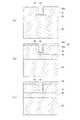
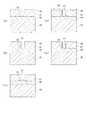
成膜ガスをプラズマ化して、穴又は溝の側壁及び底面を含む基板の表面に酸化膜を形成する成膜方法であって、
前記穴又は溝の側壁及び底面を除いた前記基板の表面に形成される酸化膜の膜厚の、前記穴又は溝の底面に形成される酸化膜の膜厚に対する膜厚比が所定の膜厚比となるように、前記穴又は溝の側壁及び底面を除く前記基板の表面に、前記穴又は溝の底面よりも厚い膜厚の酸化膜を形成する成膜方法において、
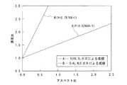
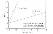
第1ガスを前記成膜ガスとして用いたときの、前記膜厚比と前記穴又は溝のアスペクト比との関係を表す直線と、前記第1ガスよりも高い膜厚比が得られる第2ガスを前記成膜ガスとして用いたときの、前記膜厚比と前記穴又は溝のアスペクト比との関係を表す直線とによって囲まれた領域内に、目標とする膜厚比がある場合には、前記第1ガスと第2ガスとの2つのガスを用いて、前記目標とする膜厚比の酸化膜を形成するようにしたことを特徴とする成膜方法に係る。
c=a(0.5288×X+1)+b(2.7576×X+1)
(但し、b=(1−a)である。)
c=a(0.4×X+1)+b(3.4×X+1)
(但し、b=(1−a)である。)
11 処理チャンバ
12 下部電極
14 上部電極
25 ガス供給装置
81 シリコン基板
87 穴
88 酸化膜
K 構造体
Claims (3)
- 成膜ガスをプラズマ化して、穴又は溝の側壁及び底面を含む基板の表面に酸化膜を形成する成膜方法であって、
前記穴又は溝の側壁及び底面を除いた前記基板の表面に形成される酸化膜の膜厚の、前記穴又は溝の底面に形成される酸化膜の膜厚に対する膜厚比が所定の膜厚比となるように、前記穴又は溝の側壁及び底面を除く前記基板の表面に、前記穴又は溝の底面よりも厚い膜厚の酸化膜を形成する成膜方法において、
前記成膜ガスとして第1ガスを用いたときの、前記膜厚比と前記穴又は溝のアスペクト比との関係を表す直線と、前記第1ガスよりも高い膜厚比が得られる第2ガスを前記成膜ガスとして用いたときの、前記膜厚比と前記穴又は溝のアスペクト比との関係を表す直線とによって囲まれた領域内に、目標とする膜厚比がある場合には、前記第1ガスと第2ガスとの2つのガスを用いて、前記目標とする膜厚比の酸化膜を形成するようにしたことを特徴とする成膜方法。 - 前記第1ガスを、テトラエトキシシラン及び酸素を含む混合ガスとし、前記第2ガスを、シラン及び亜酸化窒素を含む混合ガスとするとともに、前記第1ガス及び第2ガスのいずれか一方を用いて酸化膜を形成した後、他方のガスを用いて酸化膜を形成し、テトラエトキシシラン及び酸素から形成される酸化膜と、シラン及び亜酸化窒素から形成される酸化膜とによって、前記目標とする膜厚比の酸化膜を形成するようにしたことを特徴とする請求項1記載の成膜方法。
- 前記第1ガスを、テトラエトキシシラン及び亜酸化窒素を含む混合ガスとし、前記第2ガスを、シラン及び亜酸化窒素を含む混合ガスとするとともに、前記第1ガス及び第2ガスを同時に用いて酸化膜を形成し、テトラエトキシシラン及び亜酸化窒素から形成される酸化膜と、シラン及び亜酸化窒素から形成される酸化膜とによって、前記目標とする膜厚比の酸化膜を形成するようにしたことを特徴とする請求項1記載の成膜方法。
Priority Applications (6)
| Application Number | Priority Date | Filing Date | Title |
|---|---|---|---|
| JP2010060091AJP5052638B2 (ja) | 2010-03-17 | 2010-03-17 | 成膜方法 |
| EP10847987.4AEP2549527B1 (en) | 2010-03-17 | 2010-11-25 | Deposition method |
| KR1020127016018AKR101312002B1 (ko) | 2010-03-17 | 2010-11-25 | 성막 방법 |
| PCT/JP2010/070971WO2011114581A1 (ja) | 2010-03-17 | 2010-11-25 | 成膜方法 |
| CN201080061492.5ACN102812539B (zh) | 2010-03-17 | 2010-11-25 | 沉积方法 |
| US13/517,193US8598049B2 (en) | 2010-03-17 | 2010-11-25 | Deposition method |
Applications Claiming Priority (1)
| Application Number | Priority Date | Filing Date | Title |
|---|---|---|---|
| JP2010060091AJP5052638B2 (ja) | 2010-03-17 | 2010-03-17 | 成膜方法 |
Publications (2)
| Publication Number | Publication Date |
|---|---|
| JP2011192938A JP2011192938A (ja) | 2011-09-29 |
| JP5052638B2true JP5052638B2 (ja) | 2012-10-17 |
Family
ID=44648699
Family Applications (1)
| Application Number | Title | Priority Date | Filing Date |
|---|---|---|---|
| JP2010060091AActiveJP5052638B2 (ja) | 2010-03-17 | 2010-03-17 | 成膜方法 |
Country Status (6)
| Country | Link |
|---|---|
| US (1) | US8598049B2 (ja) |
| EP (1) | EP2549527B1 (ja) |
| JP (1) | JP5052638B2 (ja) |
| KR (1) | KR101312002B1 (ja) |
| CN (1) | CN102812539B (ja) |
| WO (1) | WO2011114581A1 (ja) |
Families Citing this family (1)
| Publication number | Priority date | Publication date | Assignee | Title |
|---|---|---|---|---|
| JP6616094B2 (ja)* | 2015-04-16 | 2019-12-04 | 株式会社iMott | 保護膜の製造方法 |
Family Cites Families (28)
| Publication number | Priority date | Publication date | Assignee | Title |
|---|---|---|---|---|
| US5643838A (en)* | 1988-03-31 | 1997-07-01 | Lucent Technologies Inc. | Low temperature deposition of silicon oxides for device fabrication |
| US5314845A (en)* | 1989-09-28 | 1994-05-24 | Applied Materials, Inc. | Two step process for forming void-free oxide layer over stepped surface of semiconductor wafer |
| JP3123061B2 (ja)* | 1990-06-13 | 2001-01-09 | ソニー株式会社 | バイアスecr―cvd法による埋め込み平坦化方法 |
| US5290358A (en)* | 1992-09-30 | 1994-03-01 | International Business Machines Corporation | Apparatus for directional low pressure chemical vapor deposition (DLPCVD) |
| US5420065A (en)* | 1993-05-28 | 1995-05-30 | Digital Equipment Corporation | Process for filling an isolation trench |
| US6180439B1 (en)* | 1996-01-26 | 2001-01-30 | Semiconductor Energy Laboratory Co., Ltd. | Method for fabricating a semiconductor device |
| JPH1092810A (ja)* | 1996-09-10 | 1998-04-10 | Mitsubishi Electric Corp | 半導体装置 |
| US6551665B1 (en)* | 1997-04-17 | 2003-04-22 | Micron Technology, Inc. | Method for improving thickness uniformity of deposited ozone-TEOS silicate glass layers |
| US6156653A (en)* | 1997-11-03 | 2000-12-05 | Zilog, Inc. | Method of fabricating a MOS device |
| JP3818561B2 (ja)* | 1998-10-29 | 2006-09-06 | エルジー フィリップス エルシーディー カンパニー リミテッド | シリコン酸化膜の成膜方法および薄膜トランジスタの製造方法 |
| JP2000150646A (ja)* | 1998-11-11 | 2000-05-30 | Sony Corp | 半導体装置およびその製造方法 |
| JP4987796B2 (ja)* | 1999-01-08 | 2012-07-25 | 株式会社東芝 | 半導体装置の製造方法 |
| US6329670B1 (en)* | 1999-04-06 | 2001-12-11 | Micron Technology, Inc. | Conductive material for integrated circuit fabrication |
| US6235608B1 (en)* | 1999-04-14 | 2001-05-22 | Winbond Electronics Corp. | STI process by method of in-situ multilayer dielectric deposition |
| US6656838B2 (en)* | 2001-03-16 | 2003-12-02 | Hitachi, Ltd. | Process for producing semiconductor and apparatus for production |
| JP2003332426A (ja)* | 2002-05-17 | 2003-11-21 | Renesas Technology Corp | 半導体装置の製造方法および半導体装置 |
| US6905940B2 (en)* | 2002-09-19 | 2005-06-14 | Applied Materials, Inc. | Method using TEOS ramp-up during TEOS/ozone CVD for improved gap-fill |
| US7097886B2 (en)* | 2002-12-13 | 2006-08-29 | Applied Materials, Inc. | Deposition process for high aspect ratio trenches |
| KR20070099913A (ko) | 2006-04-06 | 2007-10-10 | 주성엔지니어링(주) | 산화막 형성 방법 및 산화막 증착 장치 |
| US20070293034A1 (en)* | 2006-06-15 | 2007-12-20 | Macronix International Co., Ltd. | Unlanded via process without plasma damage |
| US8012846B2 (en)* | 2006-08-04 | 2011-09-06 | Taiwan Semiconductor Manufacturing Co., Ltd. | Isolation structures and methods of fabricating isolation structures |
| TWI462179B (zh)* | 2006-09-28 | 2014-11-21 | Tokyo Electron Ltd | 用以形成氧化矽膜之成膜方法與裝置 |
| US20080166880A1 (en)* | 2007-01-08 | 2008-07-10 | Levy David H | Delivery device for deposition |
| US7541298B2 (en)* | 2007-01-10 | 2009-06-02 | United Microelectronics Corp. | STI of a semiconductor device and fabrication method thereof |
| JP2009004397A (ja)* | 2007-06-19 | 2009-01-08 | Nec Electronics Corp | 半導体装置の製造方法 |
| JP4799542B2 (ja) | 2007-12-27 | 2011-10-26 | 株式会社東芝 | 半導体パッケージ |
| KR101078728B1 (ko)* | 2009-04-10 | 2011-11-01 | 주식회사 하이닉스반도체 | 반도체 소자의 절연막 형성방법 |
| US7994019B1 (en)* | 2010-04-01 | 2011-08-09 | Applied Materials, Inc. | Silicon-ozone CVD with reduced pattern loading using incubation period deposition |
- 2010
- 2010-03-17JPJP2010060091Apatent/JP5052638B2/jaactiveActive
- 2010-11-25CNCN201080061492.5Apatent/CN102812539B/zhactiveActive
- 2010-11-25EPEP10847987.4Apatent/EP2549527B1/enactiveActive
- 2010-11-25USUS13/517,193patent/US8598049B2/enactiveActive
- 2010-11-25KRKR1020127016018Apatent/KR101312002B1/koactiveActive
- 2010-11-25WOPCT/JP2010/070971patent/WO2011114581A1/jaactiveApplication Filing
Also Published As
| Publication number | Publication date |
|---|---|
| EP2549527B1 (en) | 2015-06-24 |
| WO2011114581A1 (ja) | 2011-09-22 |
| US20120258604A1 (en) | 2012-10-11 |
| EP2549527A1 (en) | 2013-01-23 |
| US8598049B2 (en) | 2013-12-03 |
| CN102812539B (zh) | 2014-10-22 |
| CN102812539A (zh) | 2012-12-05 |
| KR20120085924A (ko) | 2012-08-01 |
| JP2011192938A (ja) | 2011-09-29 |
| KR101312002B1 (ko) | 2013-09-27 |
| EP2549527A4 (en) | 2013-09-25 |
Similar Documents
| Publication | Publication Date | Title |
|---|---|---|
| TWI576912B (zh) | 減少蝕刻腔室內污染的方法 | |
| CN103733317B (zh) | 用于含硅和氮的薄膜的干式蚀刻 | |
| CN103380485B (zh) | 远程激发氟与水蒸气的蚀刻方法 | |
| JP6218836B2 (ja) | ラジカル構成要素の酸化物エッチング | |
| US7288284B2 (en) | Post-cleaning chamber seasoning method | |
| JP4228150B2 (ja) | 成膜装置、成膜方法及び記憶媒体 | |
| US20120164848A1 (en) | Method for forming nitride film | |
| JP5971870B2 (ja) | 基板処理装置、半導体装置の製造方法及び記録媒体 | |
| JPWO2019035223A1 (ja) | プラズマ生成装置、基板処理装置および半導体装置の製造方法 | |
| TW201801184A (zh) | 蝕刻介電層中之特徵部的方法 | |
| KR102152088B1 (ko) | 플라즈마 처리 방법 및 플라즈마 처리 장치 | |
| TWI479564B (zh) | Semiconductor manufacturing apparatus and semiconductor manufacturing method | |
| CN103928285A (zh) | 等离子体处理方法和等离子体处理装置 | |
| CN111540675B (zh) | 半导体制造装置及半导体装置的制造方法 | |
| US20150252479A1 (en) | Film forming apparatus, and method of manufacturing semiconductor device | |
| US12112954B2 (en) | Etching method, substrate processing apparatus, and substrate processing system | |
| US20160358811A1 (en) | Interconnect structure | |
| WO2019035314A1 (ja) | プラズマ異常判定方法、半導体装置の製造方法及び基板処理装置 | |
| JP5052638B2 (ja) | 成膜方法 | |
| CN117121170A (zh) | 基板处理方法 | |
| WO2010038887A1 (ja) | 二酸化珪素膜およびその形成方法、コンピュータ読み取り可能な記憶媒体並びにプラズマcvd装置 | |
| JP5988871B2 (ja) | ラジカルクリーニング装置及び方法 | |
| TW202333227A (zh) | 基板處理方法及電漿處理裝置 | |
| US20250113718A1 (en) | Cyclic peald/pecvd thin film encapsulation barrier | |
| JP2007096189A (ja) | プラズマcvd装置の管理方法 |
Legal Events
| Date | Code | Title | Description |
|---|---|---|---|
| A711 | Notification of change in applicant | Free format text:JAPANESE INTERMEDIATE CODE: A711 Effective date:20120126 | |
| A521 | Request for written amendment filed | Free format text:JAPANESE INTERMEDIATE CODE: A821 Effective date:20120126 | |
| A521 | Request for written amendment filed | Free format text:JAPANESE INTERMEDIATE CODE: A523 Effective date:20120216 | |
| A521 | Request for written amendment filed | Free format text:JAPANESE INTERMEDIATE CODE: A523 Effective date:20120220 | |
| A871 | Explanation of circumstances concerning accelerated examination | Free format text:JAPANESE INTERMEDIATE CODE: A871 Effective date:20120518 | |
| A621 | Written request for application examination | Free format text:JAPANESE INTERMEDIATE CODE: A621 Effective date:20120524 | |
| TRDD | Decision of grant or rejection written | ||
| A975 | Report on accelerated examination | Free format text:JAPANESE INTERMEDIATE CODE: A971005 Effective date:20120621 | |
| A01 | Written decision to grant a patent or to grant a registration (utility model) | Free format text:JAPANESE INTERMEDIATE CODE: A01 Effective date:20120626 | |
| A01 | Written decision to grant a patent or to grant a registration (utility model) | Free format text:JAPANESE INTERMEDIATE CODE: A01 | |
| A61 | First payment of annual fees (during grant procedure) | Free format text:JAPANESE INTERMEDIATE CODE: A61 Effective date:20120724 | |
| R150 | Certificate of patent or registration of utility model | Free format text:JAPANESE INTERMEDIATE CODE: R150 Ref document number:5052638 Country of ref document:JP Free format text:JAPANESE INTERMEDIATE CODE: R150 | |
| FPAY | Renewal fee payment (event date is renewal date of database) | Free format text:PAYMENT UNTIL: 20150803 Year of fee payment:3 | |
| FPAY | Renewal fee payment (event date is renewal date of database) | Free format text:PAYMENT UNTIL: 20150803 Year of fee payment:3 | |
| S531 | Written request for registration of change of domicile | Free format text:JAPANESE INTERMEDIATE CODE: R313531 | |
| FPAY | Renewal fee payment (event date is renewal date of database) | Free format text:PAYMENT UNTIL: 20150803 Year of fee payment:3 | |
| R350 | Written notification of registration of transfer | Free format text:JAPANESE INTERMEDIATE CODE: R350 | |
| R250 | Receipt of annual fees | Free format text:JAPANESE INTERMEDIATE CODE: R250 | |
| R250 | Receipt of annual fees | Free format text:JAPANESE INTERMEDIATE CODE: R250 | |
| R250 | Receipt of annual fees | Free format text:JAPANESE INTERMEDIATE CODE: R250 | |
| R250 | Receipt of annual fees | Free format text:JAPANESE INTERMEDIATE CODE: R250 | |
| R250 | Receipt of annual fees | Free format text:JAPANESE INTERMEDIATE CODE: R250 | |
| R250 | Receipt of annual fees | Free format text:JAPANESE INTERMEDIATE CODE: R250 | |
| S531 | Written request for registration of change of domicile | Free format text:JAPANESE INTERMEDIATE CODE: R313531 | |
| R350 | Written notification of registration of transfer | Free format text:JAPANESE INTERMEDIATE CODE: R350 | |
| R250 | Receipt of annual fees | Free format text:JAPANESE INTERMEDIATE CODE: R250 | |
| R250 | Receipt of annual fees | Free format text:JAPANESE INTERMEDIATE CODE: R250 | |
| R250 | Receipt of annual fees | Free format text:JAPANESE INTERMEDIATE CODE: R250 | |
| R250 | Receipt of annual fees | Free format text:JAPANESE INTERMEDIATE CODE: R250 | |
| R250 | Receipt of annual fees | Free format text:JAPANESE INTERMEDIATE CODE: R250 |