JP5042865B2 - Display device - Google Patents
Display deviceDownload PDFInfo
- Publication number
- JP5042865B2 JP5042865B2JP2007557637AJP2007557637AJP5042865B2JP 5042865 B2JP5042865 B2JP 5042865B2JP 2007557637 AJP2007557637 AJP 2007557637AJP 2007557637 AJP2007557637 AJP 2007557637AJP 5042865 B2JP5042865 B2JP 5042865B2
- Authority
- JP
- Japan
- Prior art keywords
- fluid
- pixel
- sub
- boundary
- support plate
- Prior art date
- Legal status (The legal status is an assumption and is not a legal conclusion. Google has not performed a legal analysis and makes no representation as to the accuracy of the status listed.)
- Active
Links
Images


Classifications
- G—PHYSICS
- G02—OPTICS
- G02B—OPTICAL ELEMENTS, SYSTEMS OR APPARATUS
- G02B26/00—Optical devices or arrangements for the control of light using movable or deformable optical elements
- G02B26/004—Optical devices or arrangements for the control of light using movable or deformable optical elements based on a displacement or a deformation of a fluid
- G02B26/005—Optical devices or arrangements for the control of light using movable or deformable optical elements based on a displacement or a deformation of a fluid based on electrowetting
- G—PHYSICS
- G02—OPTICS
- G02B—OPTICAL ELEMENTS, SYSTEMS OR APPARATUS
- G02B26/00—Optical devices or arrangements for the control of light using movable or deformable optical elements
- G02B26/004—Optical devices or arrangements for the control of light using movable or deformable optical elements based on a displacement or a deformation of a fluid
- G—PHYSICS
- G02—OPTICS
- G02B—OPTICAL ELEMENTS, SYSTEMS OR APPARATUS
- G02B26/00—Optical devices or arrangements for the control of light using movable or deformable optical elements
- G02B26/007—Optical devices or arrangements for the control of light using movable or deformable optical elements the movable or deformable optical element controlling the colour, i.e. a spectral characteristic, of the light
- G—PHYSICS
- G02—OPTICS
- G02B—OPTICAL ELEMENTS, SYSTEMS OR APPARATUS
- G02B5/00—Optical elements other than lenses
- G02B5/02—Diffusing elements; Afocal elements
- G02B5/0273—Diffusing elements; Afocal elements characterized by the use
- G02B5/0284—Diffusing elements; Afocal elements characterized by the use used in reflection
Landscapes
- Physics & Mathematics (AREA)
- General Physics & Mathematics (AREA)
- Optics & Photonics (AREA)
- Astronomy & Astrophysics (AREA)
- Spectroscopy & Molecular Physics (AREA)
- Devices For Indicating Variable Information By Combining Individual Elements (AREA)
- Electrochromic Elements, Electrophoresis, Or Variable Reflection Or Absorption Elements (AREA)
- Control Of Indicators Other Than Cathode Ray Tubes (AREA)
- Mechanical Light Control Or Optical Switches (AREA)
- Vehicle Body Suspensions (AREA)
- Diaphragms For Electromechanical Transducers (AREA)
- Measuring Pulse, Heart Rate, Blood Pressure Or Blood Flow (AREA)
Abstract
Description
Translated fromJapanese本発明は、表示装置に関し、画素を有し、各画素が第1の支持プレートと第2の支持プレートとの間の空間内で互いに不混和性の少なくとも1つの第1の流体と第2の流体とを有し、当該第2の流体が電気伝導性又は有極性のものである表示装置に関する。 The present invention relates to a display device, which includes pixels, each pixel being immiscible with each other in a space between a first support plate and a second support plate, and a second fluid. A display device in which the second fluid is electrically conductive or polar.
TFT−LCDのような表示装置は、ラップトップコンピュータ及び電子手帳に用いられているが、GSM電話においても益々拡大する用途を見出している。LCDに代わり、例えば(ポリマ)LED表示装置も用いられつつある。 Display devices such as TFT-LCDs are used in laptop computers and electronic notebooks, but have found increasing use in GSM phones. Instead of LCDs, for example, (polymer) LED display devices are also being used.
これまで十分に確立されているこれら表示効果とは別に、ペーパホワイト用途に適した電気泳動ディスプレイのような他の表示技術が進化しつつある。 Apart from these well-established display effects, other display technologies such as electrophoretic displays suitable for paper white applications are evolving.
より包括的には、本発明は、第1の支持プレートと第2の支持プレートとの間の空間内で互いに不混和性の少なくとも1つの第1の流体と第2の流体とを有し、当該第2の流体が電気伝導性又は有極性のものである光学スイッチに関する。 More generally, the present invention comprises at least one first fluid and second fluid that are immiscible with each other in the space between the first support plate and the second support plate, The present invention relates to an optical switch in which the second fluid is electrically conductive or polar.
光学スイッチは、シャッタ用途、ダイヤフラムだけでなく、例えばディスプレイ用途におけるスイッチ可能なカラーフィルタにも用いることができる。 The optical switch can be used not only for shutter applications and diaphragms but also for switchable color filters in display applications, for example.
本発明は、エレクトロウェッティング(electro-wetting)と呼ばれる原理に基づいている。本発明は、この原理を用いる新しい態様であって、第1の状態で当該流体の1つを第1の支持プレートの比較的大なる部分に隣接させ、第2の状態では他の流体を少なくとも一部、当該第1の支持プレートに隣接させるものを提供する。 The present invention is based on a principle called electro-wetting. The present invention is a new embodiment using this principle, in which one of the fluids is adjacent to a relatively large portion of the first support plate in a first state and at least another fluid is in the second state. Some are provided adjacent to the first support plate.
例えば(第1の)流体が(着色した)オイルで、第2の(他の)流体が水(界面張力のため)である場合、水の層とオイルの層を有する2層システムが設けられる。しかし、水と第1の支持プレート上の電極との間に電圧が印加されると、オイルの層は、静電気力により脇へ動き、或いは崩壊する。水の部分はこのときオイルの層を貫通するので、画素は部分的に透明になる。(拡散性の)反射器が画素の中又は下のオイルに位置づけられる場合には、反射型ディスプレイが実現される。 For example, if the (first) fluid is (colored) oil and the second (other) fluid is water (due to interfacial tension), a two-layer system with a water layer and an oil layer is provided. . However, when a voltage is applied between the water and the electrode on the first support plate, the oil layer moves aside or collapses due to electrostatic forces. Since the water part then penetrates the oil layer, the pixel becomes partially transparent. A reflective display is realized if the (diffusive) reflector is positioned in the oil in or below the pixel.
この原理に基づく表示装置は、PCT出願WO03/00196(PH−NL02.0129)に記述されている。この出願に示される全ての実施例において、画素壁部が画素全体の厚さにわたり延びていない画素が説明されており、第2の状態において他の流体が第1の支持プレートにほぼ完全に隣接する。画素(ピクセル)が規定された空間(例えば、実質的に閉じた空間)に対応することを可能にすることができるような、この出願に示されていない実施例も可能である。 A display device based on this principle is described in PCT application WO03 / 00196 (PH-NL02.129). In all embodiments shown in this application, a pixel is described in which the pixel wall does not extend across the entire pixel thickness, and in the second state, other fluid is almost completely adjacent to the first support plate. To do. Embodiments not shown in this application are also possible, which can allow a picture element (pixel) to correspond to a defined space (eg, a substantially closed space).
この表示装置は、電圧が印加されたときの状態では漏れ電流が少ないので低電力消費を呈する。しかしながら、電子書籍のような幾つかの用途においては、極めて低い電力消費が望まれる。また、中間的な透過又は反射の値(濃淡値)を有するこうした用途における反射型ディスプレイの需要が益々増えている。 This display device exhibits low power consumption because there is little leakage current when voltage is applied. However, in some applications such as electronic books, very low power consumption is desired. There is also an increasing demand for reflective displays in such applications with intermediate transmission or reflection values (shading values).
本発明の目的の1つは、上述した問題を少なくとも一部克服することである。 One object of the present invention is to overcome at least in part the problems described above.
このため、本発明によれば、本装置は、副画素を画定するように第1の流体を分離する境界部が画像領域内に第1の支持プレート上に設けられ、当該第1の支持プレートは、副画素毎に電極を有する。(局部的)電圧の印加なしでオイルの動きを防止する境界部が画素(ピクセル)内に組み入れられると、当該システムにおいて双安定性が実現され、すなわち電圧がなくなっても当該システムの光学的状態が不変になる。このようにして、電力消費が低減される。 For this reason, according to the present invention, the apparatus is provided with a boundary portion for separating the first fluid so as to define the sub-pixels in the image area on the first support plate. Has an electrode for each sub-pixel. When a boundary that prevents the movement of oil without applying a (local) voltage is incorporated in the pixel, bistability is achieved in the system, i.e. the optical state of the system even when there is no voltage. Becomes immutable. In this way, power consumption is reduced.
好適実施例において、当該境界部は、壁部に設けられた、より湿潤性の高い表面を有する。 In a preferred embodiment, the boundary has a more wettable surface provided on the wall.
低下した電力の使用とは別に、双安定性のさらなる利点の1つは、双安定表示装置において濃淡値を得るためのその方法自体その技術において知られているならば、画素の領域を異なる領域に分割することによって濃淡値を得ることの実現性である。 Apart from the use of reduced power, one of the further advantages of bistability is that if the method itself for obtaining gray values in a bistable display device is known per se in the art, the region of the pixel is different from that of the region. This is the feasibility of obtaining a gray value by dividing into two.
但し、本発明の他の好適実施例は、電極のうちの1つにパルス状の高電圧を印加し当該パルスが境界部全体にわたりオイルが動くのに必要とされる時間よりも短いものとすることによりアナログの階調を得ることの実現性を提供する。 However, other preferred embodiments of the present invention apply a pulsed high voltage to one of the electrodes and the pulse is shorter than the time required for the oil to move across the boundary. This provides the feasibility of obtaining analog tones.
本発明のこれらの態様及びその他の態様は、以下に説明する実施例に基づいて明らかとなる。 These and other aspects of the invention will be apparent from the examples described below.
図面は、概略的なものであり一律の尺度で描いたものではない。対応する要素は、概して同じ参照番号により示される。 The drawings are schematic and are not drawn to scale. Corresponding elements are generally indicated by the same reference numerals.
図1は、例えば1つの画素のような表示装置1の一部の概略的断面を示し、本発明による表示装置の基礎を形成する原理を示している。2つの透明基板又は支持プレート3,4の間には、第1の流体5と第2の流体6が設けられ、これらは、互いに不混和性のものとされる。第1の流体5は、例えばヘキサデカンのような又は本例では(シリコン)オイルのようなアルカンとされる。第2の流体6は、例えば水又は塩溶液(例えば、水とエチルアルコールとの混合物におけるKClの溶液)などの電気的伝導性又は有極性のものとされる。本例では透明基板7の下で、オイルの下に位置づけられる拡散反射器10によって、反射型ディスプレイ画素が実現される。 FIG. 1 shows a schematic cross-section of a part of a display device 1 such as, for example, one pixel and shows the principle that forms the basis of a display device according to the invention. A
第1の状態において、外部電圧が印加されていない場合(図1a)、流体5,6は、例えばガラス又はプラスチックの第1及び第2の透明支持プレート3,4に隣接する。第1の支持プレート3上には、例えばインジウム(スズ)酸化物のような透明電極7と、本例ではアモルファスフルオロポリマ(AF1600)とされる低湿潤性(疎水性)の中間層8が設けられる。画素の全領域にわたるオイルの存在により、黒が現われる(矢印11)。 In the first state, when no external voltage is applied (FIG. 1a), the
相互接続部20,21を介して電圧が印加される(電圧源9)場合、層5は、脇に動き小滴群に崩壊する(図1b)。これは、静電気エネルギ利得が湾曲した表面の形成による表面エネルギ損失よりも大きいときに起こる。この場合、画素の主たる領域で光が反射する一方、小さな部分だけが黒を表す(矢印12)。 When a voltage is applied via the interconnects 20, 21 (voltage source 9), the
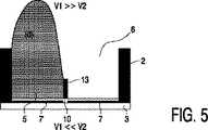
図2は、本発明による表示装置の一部の平面図を示しており、図3〜図7は、図2における線III−IIIに沿う概略的断面を示している。所定の駆動状態においてオイルの動きを防止する他の親水性の境界部すなわち壁部13が画素に組み込まれる。FIG. 2 shows a plan view of a part of the display device according to the invention, and FIGS. 3 to 7 show schematic cross sections along the line III-III in FIG. Boundary That
画素壁部2は、画素の厚さ全体にわたり延在する必要がない。壁部2,13は、当該技術において知られているフォトリソグラフィ、オフセット印刷又は他の印刷技術により得ることができる。他の参照番号は、図1におけるものと同じ意味を有する。 The
本例における境界部13は、画素を等しいサイズを有する2つのセグメントに分割する。また、画素は、個々にアドレス指定可能な等しいサイズの2つの電極7,7´を有する。当該境界部13(これは可能な限り狭く選定される)に対し、親水性となるような材料が選定される。これは、オイル5が当該境界部を湿らすこと、特に当該境界部の頂部を湿らすることを防止することを意味する。後者の点は、境界部すなわち壁部13の頂部に、より湿潤性の高い表面13´を形成することにより達成可能である。同時に、画素壁部2の材料よりも低い親水性になるように選ばれる。これにより、電極7,7´のどちらか又は双方への電圧印加が近隣の副画素のうちの一方にオイルを移動させることになる、という効果を奏する。以下で説明する例における全ての電圧は、第2の流体6にかけられるグランド電位に対して選定されるものである。The
図3において、オイル5は、両方の画素部分にわたり均等に分布させられる。これは、V1(電極7に印加されるもの)及びV2(電極7´に印加されるもの)が等しくかつどちらも大きさが小さい場合に達成される。 In FIG. 3, the
壁部13の側部上の当該オイルの固着は、当該2つのオイル体積の分離を確実にするよう十分に強いものとなっている。但し、V1又はV2のどちらかが増大したときには、或るポイントで、オイルは当該境界部を濡らそうとする傾向となる。何故なら、比較的高い電圧を有する電極の領域では下側にある基板2(又は反射層10)が壁部13自体よりも高い親水性となるからである。この結果、オイルは壁部13を横断して他の側へ移動することになり、図4(V1>>V2)又は図5(V1<<V2)に示される状況となる。 The oil sticking on the side of the
画素を最暗状態(オイルが図6に示されるように均等に分布させられる状態)にリセットするため、両方の副画素に高い電圧が印加され、画素の下にある表面は壁部13よりも高い親水性のものとなる。この結果、オイル5は、壁部13をわたって動き、図6におけるが如く画素全体にわたり再分布することになる。電圧を解除すると、今度は画素の下にある表面よりも高い親水性になるので、壁部13においてオイル層を分裂させることになる。ここで選定される電極構成は、一例に過ぎない。電極7,7´に対して等しい面積を選ぶことにより、実際上、図5及び図6の双方の状況は、同様の反射(又は透過)特性すなわち中間のグレーを呈する。 In order to reset the pixel to the darkest state (oil distributed evenly as shown in FIG. 6), a high voltage is applied to both sub-pixels, and the surface under the pixel is more than the
図7は、アナログ階調の安定した濃淡値をタイミングを用いることによりどのようにして得られるかを示している。図3に示される状況においてパルス状の高電圧が電極7,7´のうちの一方に印加され、そのパルスがオイルを壁部13全体にわたり動かすのに必要な時間よりも短いものとすると、その最終状態において、当該オイル膜は、画素の一方の部分において当該他方におけるものよりも厚くなる。当該膜の公称の厚さは光の約1%が反射するようなものなので、当該膜が厚くなったところの部分においてそれほど反射率が低下することはない。但し、当該オイル膜が薄くなっている部分の反射率は大幅に増大することになり、この結果、画素の反射率の全体が増加することになる。このようにして、オイルが動くのにかかる時間に対するパルス長に応じて、アナログ階調の安定した濃淡値が得られる。 FIG. 7 shows how a stable gray value of analog gradation can be obtained by using timing. In the situation shown in FIG. 3, if a pulsed high voltage is applied to one of the
ここで選定される電極構成は、一例に過ぎない。円形形状のような他の電極構成も採用可能である。2つのピクセル部分の領域は、異なるものとすることができ、これにより複数の濃淡値が得られる。 The electrode configuration selected here is only an example. Other electrode configurations such as circular shapes can also be employed. The areas of the two pixel portions can be different, resulting in multiple gray values.
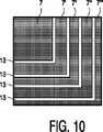
図8は、画素領域が或る特定の面積比を有する4つの部分7,7´,7´´,7´´´に分割され電圧V1,V2,V3,V4により駆動される電極構成を示している。図9は、画素領域が別の面積比を有する3つの部分7,7´,7´´に分割され電圧V1,V2及びV3により駆動される電極構成を示している。図10は、連続した画素領域部7´,7´´,7´´´により囲まれている中央の画素領域7を有する電極構成を示している。これらの部分は、図11に示されるように、必ずしも正方形又は長方形である必要はない。 FIG. 8 shows an electrode configuration in which the pixel region is divided into four
原理の幾つかの変形は可能である。反射型装置を説明したが、ディスプレイを透過型としてもよい。また、壁部13の高さを変えてもよく、その壁部が例えば湾曲面を有するものとしてもよい。当該高さの変更は、固定状態のオイルの曲率を変更することになるので、必要な電圧及び当該状態の安定性に影響を与えることになる。境界部13の材料が画素壁部2に用いられる材料と同じである場合、画素壁部のように等しく親水性のものとされ、ここでは境界部13の高さ(これは常に画素壁部よりも低いものとされゼロとすることさえ可能であり、副画素を駆動する位置において相当に強い親水性、場合によっては画素壁部2のものよりもさらに強いものとすることを必要とする場合がある)が画素の動的性能を決めるパラメータとなる。この場合、画素サイズに対するオイルの体積は、重要な役目を担うことになる。画素全体を満たすのに、すなわち両方の電極が高電圧に切り換えられた場合に低めの境界部にわたって満たすのに十分なオイルがあるのがよい。 Several variations of the principle are possible. Although the reflection type device has been described, the display may be a transmission type. Further, the height of the
本発明は、ありとあらゆる新規な特徴的事項及び特徴的事項のありとあらゆる組み合わせに存するものである。請求項における参照符号は、それらの保護範囲を限定するものではない。「有する」なる動詞及びその活用形の使用は、当該請求項に記載されたもの以外の要素の存在を排除するものではない。要素の単数表現は、そのような要素の複数の存在を排除するものではない。 The present invention resides in every and every novel feature and every combination of features. Reference numerals in the claims do not limit their protective scope. The use of the verb “comprise” and its conjugations does not exclude the presence of elements other than those stated in the claims. The singular representation of an element does not exclude the presence of a plurality of such elements.
Claims (11)
Translated fromJapanese各画素は、
第1の透光性支持プレート(3)と、
第2の支持プレート(4)と、
少なくとも1つの第1の流体(5)と、
前記第1の流体(5)とは不混和性であり、電気的伝導性又は有極性である第2の流体(6)と、
を備え、
前記第1の流体(5)及び前記第2の流体(6)は、前記第1の透光性支持プレート(3)と前記第2の支持プレート(4)との間の空間に位置しており、
境界部(13)は、前記空間を異なる副画素に分割しており、
副画素の表面領域は、前記第2の流体に対して湿潤性が低く、高い湿潤性の表面領域を有する境界部(13)により他の副画素から分離されており、
前記第1の透光性支持プレート(3)は、各副画素の電極(7)を有しており、
前記境界部は、前記第1の流体(5)を前記副画素に対応する容量に分離し、かつ、第1副画素と第2副画素との間で、前記第1の流体(5)の伝搬を可能にし、
前記第2副画素に十分に高い電圧を印加することによって、前記第2副画素の表面は、前記第2の流体に対して前記境界部(13)よりも湿潤性が高くなり、前記第1の流体(5)は前記境界部(13)を移動可能となり、前記第1副画素に移動し、
電圧印加の解除により、前記境界部(13)は、前記第1及び前記第2副画素の表面よりも湿潤性が高くなり、前記第1の流体(5)は前記境界部(13)により分離される、表示装置。A display device having pixelsseparated by a wall (2) ,
Each pixel is
A first translucent support plate (3);
A second support plate (4);
At least one first fluid (5);
A second fluid (6) that is immiscible with the first fluid (5) and is electrically conductive or polar;
With
The first fluid (5) and the second fluid (6) are located in a space between the first translucent support plate (3) and the second support plate (4). And
The boundary (13) divides the space into different subpixels,
The surface area of the sub-pixel is low wettability to the second fluid andis separated from other sub-pixels by aboundary portion (13) having a highly wettable surface area,
The first translucent support plate (3) has an electrode (7)for each sub-pixel,
The boundary part separates the first fluid (5) into a capacity corresponding to the sub-pixel, and betweenthe first sub-pixel andthe second sub-pixel, the first fluid (5) Allows propagation,
By applying a sufficiently high voltage to the second subpixel, the surface of the second subpixel becomes more wettable than the boundary portion (13) with respect to the second fluid, and the first subpixel is exposed to the first subpixel. Fluid (5) is movable along the boundary (13), moves to the first sub-pixel,
By releasing the voltage application, the boundary portion (13) becomes wettable than the surfaces of the first and second subpixels, and the first fluid (5) is separated by the boundary portion (13). by Ru, display device.
第2の支持プレート(4)と、
少なくとも1つの第1の流体(5)と、
前記第1の流体(5)とは不混和性であり、電気的伝導性又は有極性である第2の流体(6)と、
を備え、
前記第1の流体(5)及び前記第2の流体(6)は、前記第1の透光性支持プレート(3)と前記第2の支持プレート(4)との間の空間に位置しており、
境界部(13)は、前記空間を異なる副画素に分割しており、
副画素の表面領域は、前記第2の流体に対して湿潤性が低く、高い湿潤性の表面領域を有する境界部(13)により他の副画素から分離されており、
前記第1の透光性支持プレート(3)は、各副画素の電極(7)を有しており、
前記境界部は、前記第1の流体(5)を前記副画素に対応する容量に分離し、かつ、第1副画素と第2副画素との間で、前記第1の流体(5)の伝搬を可能にし、
前記第2副画素に十分に高い電圧を印加することによって、前記第2副画素の表面は、前記第2の流体に対して前記境界部(13)よりも湿潤性が高くなり、前記第1の流体(5)は前記境界部(13)を移動可能となり、前記第1副画素に移動し、
電圧印加の解除により、前記境界部(13)は、前記第1及び前記第2副画素の表面よりも湿潤性が高くなり、前記第1の流体(5)は前記境界部(13)により分離される、光学スイッチ。A first translucent support plate (3);
A second support plate (4);
At least one first fluid (5);
A second fluid (6) that is immiscible with the first fluid (5) and is electrically conductive or polar;
With
The first fluid (5) and the second fluid (6) are located in a space between the first translucent support plate (3) and the second support plate (4). And
The boundary (13) divides the space into different subpixels,
The surface area of the sub-pixel is low wettability to the second fluid andis separated from other sub-pixels by aboundary portion (13) having a highly wettable surface area,
The first translucent support plate (3) has an electrode (7)for each sub-pixel,
The boundary part separates the first fluid (5) into a capacity corresponding to the sub-pixel, and betweenthe first sub-pixel andthe second sub-pixel, the first fluid (5) Allows propagation,
By applying a sufficiently high voltage to the second subpixel, the surface of the second subpixel becomes more wettable than the boundary portion (13) with respect to the second fluid, and the first subpixel is exposed to the first subpixel. Fluid (5) is movable along the boundary (13), moves to the first sub-pixel,
By releasing the voltage application, the boundary portion (13) becomes wettable than the surfaces of the first and second subpixels, and the first fluid (5) is separated by the boundary portion (13). It is is, the optical switch.
Applications Claiming Priority (3)
| Application Number | Priority Date | Filing Date | Title |
|---|---|---|---|
| EP05101497.5 | 2005-02-28 | ||
| EP05101497 | 2005-02-28 | ||
| PCT/IB2006/050528WO2006090317A1 (en) | 2005-02-28 | 2006-02-17 | Display device |
Publications (2)
| Publication Number | Publication Date |
|---|---|
| JP2008532082A JP2008532082A (en) | 2008-08-14 |
| JP5042865B2true JP5042865B2 (en) | 2012-10-03 |
Family
ID=36366230
Family Applications (1)
| Application Number | Title | Priority Date | Filing Date |
|---|---|---|---|
| JP2007557637AActiveJP5042865B2 (en) | 2005-02-28 | 2006-02-17 | Display device |
Country Status (8)
| Country | Link |
|---|---|
| US (2) | US9086565B2 (en) |
| EP (1) | EP1856571B1 (en) |
| JP (1) | JP5042865B2 (en) |
| CN (1) | CN100576014C (en) |
| AT (1) | ATE453874T1 (en) |
| DE (1) | DE602006011441D1 (en) |
| TW (1) | TW200643585A (en) |
| WO (1) | WO2006090317A1 (en) |
Families Citing this family (30)
| Publication number | Priority date | Publication date | Assignee | Title |
|---|---|---|---|---|
| GB0611134D0 (en)* | 2006-06-06 | 2006-07-19 | Liquavista Bv | Optical apparatus |
| TWI442086B (en)* | 2006-08-31 | 2014-06-21 | Liquavista Bv | Electronic device comprising an array of cells and method for operating the same |
| JP5130726B2 (en)* | 2007-01-26 | 2013-01-30 | 大日本印刷株式会社 | Display device and display medium using the same |
| JP2009211047A (en)* | 2008-02-05 | 2009-09-17 | Sony Corp | Liquid optical element |
| WO2009141938A1 (en)* | 2008-05-19 | 2009-11-26 | シャープ株式会社 | Display device |
| KR101544588B1 (en)* | 2009-01-29 | 2015-08-21 | 삼성전자주식회사 | Reflective display device using dielectrophoresis and manufacturing method thereof |
| DE102009001310A1 (en)* | 2009-03-03 | 2010-09-09 | Seereal Technologies S.A. | Display with an active matrix of electrowetting cells |
| GB0908681D0 (en)* | 2009-05-20 | 2009-07-01 | Liquavista Bv | Method of manufacturing an optical display |
| GB0922690D0 (en) | 2009-12-30 | 2010-02-17 | Liquavista Bv | Electrowetting display device |
| US8643934B2 (en) | 2010-09-03 | 2014-02-04 | Industrial Technology Research Institute | Display |
| US8693081B2 (en)* | 2010-09-30 | 2014-04-08 | University Of Cincinnati | Electrofluidic imaging film, devices, and displays, and methods of making and using the same |
| KR20130021703A (en) | 2011-08-23 | 2013-03-06 | 삼성디스플레이 주식회사 | Electro wetting display device |
| GB201117556D0 (en)* | 2011-10-11 | 2011-11-23 | Samsung Lcd Nl R & D Ct Bv | Display apparatus |
| US9804607B1 (en)* | 2011-11-16 | 2017-10-31 | Zane Coleman | Fluid transfer systems, devices, components, and methods of manufacture |
| US10401876B1 (en) | 2011-11-16 | 2019-09-03 | Zane Coleman | Fluid collection component comprising a film with fluid channels |
| GB201121732D0 (en)* | 2011-12-16 | 2012-02-01 | Samsung Lcd Nl R & D Ct Bv | Electrowetting display device |
| KR101933718B1 (en)* | 2012-03-27 | 2018-12-28 | 리쿠아비스타 비.브이. | Electro wetting display device |
| KR101941712B1 (en)* | 2012-06-05 | 2019-01-24 | 리쿠아비스타 비.브이. | Electrowetting display device and fabrication method of the same |
| KR101976209B1 (en) | 2012-08-28 | 2019-05-07 | 리쿠아비스타 비.브이. | Electrowetting display device |
| JP6204654B2 (en)* | 2012-11-22 | 2017-09-27 | 富士フイルム株式会社 | Method for producing dye composition for electrowetting display, and method for producing electrowetting display device |
| US9110284B2 (en)* | 2013-09-25 | 2015-08-18 | Amazon Technologies, Inc. | Electrowetting element |
| US10018828B2 (en)* | 2014-12-22 | 2018-07-10 | Amazon Technologies, Inc. | Electrowetting display device with stable display states |
| US10235948B2 (en) | 2016-06-29 | 2019-03-19 | Amazon Technologies, Inc. | Electrowetting element with stable fluid configurations |
| US10241320B2 (en)* | 2016-06-29 | 2019-03-26 | Amazon Technologies, Inc. | Electrowetting element with shaped support plate surface portion |
| US9952423B2 (en) | 2016-06-29 | 2018-04-24 | Amazon Technologies, Inc. | Method of controlling an electrowetting element with stable fluid configurations |
| WO2018002245A1 (en)* | 2016-06-29 | 2018-01-04 | Amazon Technologies, Inc. | Electrowetting element with stable fluid configurations |
| US10504458B1 (en)* | 2017-06-08 | 2019-12-10 | Amazon Technologies, Inc. | Electrowetting element with multiple electrodes |
| US10546544B1 (en) | 2017-06-08 | 2020-01-28 | Amazon Technologies, Inc. | Electrowetting element with multiple electrodes |
| US10475401B1 (en) | 2017-06-08 | 2019-11-12 | Amazon Technologies, Inc. | Electrowetting element with multiple electrodes |
| JP6647738B2 (en)* | 2017-06-12 | 2020-02-14 | 矢崎総業株式会社 | Battery pack |
Family Cites Families (16)
| Publication number | Priority date | Publication date | Assignee | Title |
|---|---|---|---|---|
| US5181016A (en)* | 1991-01-15 | 1993-01-19 | The United States Of America As Represented By The United States Department Of Energy | Micro-valve pump light valve display |
| CN1268979C (en)* | 2001-06-05 | 2006-08-09 | 皇家菲利浦电子有限公司 | Display device based on frustrated total internal reflection |
| JP2005518335A (en) | 2001-06-25 | 2005-06-23 | ソシエテ・ドゥ・コンセイユ・ドゥ・ルシェルシュ・エ・ダプリカーション・シャンティフィック・エス・ア・エス | Pharmaceutical composition for inhibiting the growth of pituitary adenoma and method of using same |
| US6674934B2 (en) | 2001-11-06 | 2004-01-06 | Agilent Technologies, Inc. | Pressure-actuated bi-stable optical switching |
| CN1633622A (en) | 2002-02-19 | 2005-06-29 | 皇家飞利浦电子股份有限公司 | display device |
| US7649674B2 (en)* | 2002-06-10 | 2010-01-19 | E Ink Corporation | Electro-optic display with edge seal |
| JP2004144998A (en)* | 2002-10-24 | 2004-05-20 | Hitachi Ltd | Image display device |
| US7359108B2 (en)* | 2003-01-27 | 2008-04-15 | Liquavista B.V. | Display device |
| EP1599752A1 (en) | 2003-02-26 | 2005-11-30 | Koninklijke Philips Electronics N.V. | A passive matrix display with bistable electro-wetting cells |
| US20040191127A1 (en)* | 2003-03-31 | 2004-09-30 | Avinoam Kornblit | Method and apparatus for controlling the movement of a liquid on a nanostructured or microstructured surface |
| KR101100980B1 (en)* | 2003-05-22 | 2011-12-29 | 삼성 엘씨디 네덜란드 알앤디 센터 비.브이. | Display devices |
| WO2004104671A1 (en)* | 2003-05-22 | 2004-12-02 | Koninklijke Philips Electronics N.V. | Display device |
| US6847493B1 (en)* | 2003-08-08 | 2005-01-25 | Lucent Technologies Inc. | Optical beamsplitter with electro-wetting actuation |
| CN101930118B (en)* | 2003-10-08 | 2013-05-29 | 伊英克公司 | Electro-wetting displays |
| EP1761819A1 (en) | 2004-06-23 | 2007-03-14 | Koninklijke Philips Electronics N.V. | Bi-stable electrowetting optical element and driving method therefore |
| WO2006017129A2 (en)* | 2004-07-09 | 2006-02-16 | University Of Cincinnati | Display capable electrowetting light valve |
- 2006
- 2006-02-17JPJP2007557637Apatent/JP5042865B2/enactiveActive
- 2006-02-17CNCN200680006180Apatent/CN100576014C/enactiveActive
- 2006-02-17EPEP06710935Apatent/EP1856571B1/enactiveActive
- 2006-02-17DEDE602006011441Tpatent/DE602006011441D1/enactiveActive
- 2006-02-17ATAT06710935Tpatent/ATE453874T1/ennot_activeIP Right Cessation
- 2006-02-17USUS11/816,716patent/US9086565B2/enactiveActive
- 2006-02-17WOPCT/IB2006/050528patent/WO2006090317A1/enactiveApplication Filing
- 2006-02-24TWTW095106396Apatent/TW200643585A/enunknown
- 2015
- 2015-07-20USUS14/804,066patent/US10120183B2/enactiveActive
Also Published As
| Publication number | Publication date |
|---|---|
| DE602006011441D1 (en) | 2010-02-11 |
| US10120183B2 (en) | 2018-11-06 |
| EP1856571A1 (en) | 2007-11-21 |
| US9086565B2 (en) | 2015-07-21 |
| CN100576014C (en) | 2009-12-30 |
| EP1856571B1 (en) | 2009-12-30 |
| TW200643585A (en) | 2006-12-16 |
| CN101128767A (en) | 2008-02-20 |
| JP2008532082A (en) | 2008-08-14 |
| WO2006090317A1 (en) | 2006-08-31 |
| ATE453874T1 (en) | 2010-01-15 |
| US20080204370A1 (en) | 2008-08-28 |
| US20160018634A1 (en) | 2016-01-21 |
Similar Documents
| Publication | Publication Date | Title |
|---|---|---|
| JP5042865B2 (en) | Display device | |
| JP4653398B2 (en) | Display device | |
| US7359108B2 (en) | Display device | |
| US9664891B2 (en) | Electrowetting element with controlled fluid motion | |
| KR101016976B1 (en) | 2d/3d display apparatus | |
| JP4610561B2 (en) | Display device | |
| CN100373208C (en) | display screen | |
| CN101903827B (en) | Display element and electrical equipment using the display element | |
| CN101681584B (en) | Display device and electrical equipment utilizing the same | |
| CN101223475A (en) | Display element and electronic device using same | |
| CN101681580A (en) | Display element and electronic device using the same | |
| CN107092088A (en) | A kind of bistable electro wetting board structure and display device | |
| WO2012066970A1 (en) | Display element and electrical appliance using same | |
| JP2009294246A (en) | Display element and electric device using the same |
Legal Events
| Date | Code | Title | Description |
|---|---|---|---|
| A621 | Written request for application examination | Free format text:JAPANESE INTERMEDIATE CODE: A621 Effective date:20090216 | |
| A131 | Notification of reasons for refusal | Free format text:JAPANESE INTERMEDIATE CODE: A131 Effective date:20110630 | |
| A711 | Notification of change in applicant | Free format text:JAPANESE INTERMEDIATE CODE: A711 Effective date:20110705 | |
| A521 | Request for written amendment filed | Free format text:JAPANESE INTERMEDIATE CODE: A523 Effective date:20110927 | |
| A131 | Notification of reasons for refusal | Free format text:JAPANESE INTERMEDIATE CODE: A131 Effective date:20111025 | |
| A521 | Request for written amendment filed | Free format text:JAPANESE INTERMEDIATE CODE: A523 Effective date:20120120 | |
| A131 | Notification of reasons for refusal | Free format text:JAPANESE INTERMEDIATE CODE: A131 Effective date:20120306 | |
| A521 | Request for written amendment filed | Free format text:JAPANESE INTERMEDIATE CODE: A523 Effective date:20120605 | |
| TRDD | Decision of grant or rejection written | ||
| A01 | Written decision to grant a patent or to grant a registration (utility model) | Free format text:JAPANESE INTERMEDIATE CODE: A01 Effective date:20120703 | |
| A01 | Written decision to grant a patent or to grant a registration (utility model) | Free format text:JAPANESE INTERMEDIATE CODE: A01 | |
| A61 | First payment of annual fees (during grant procedure) | Free format text:JAPANESE INTERMEDIATE CODE: A61 Effective date:20120711 | |
| R150 | Certificate of patent or registration of utility model | Ref document number:5042865 Country of ref document:JP Free format text:JAPANESE INTERMEDIATE CODE: R150 | |
| FPAY | Renewal fee payment (event date is renewal date of database) | Free format text:PAYMENT UNTIL: 20150720 Year of fee payment:3 | |
| S533 | Written request for registration of change of name | Free format text:JAPANESE INTERMEDIATE CODE: R313533 | |
| R350 | Written notification of registration of transfer | Free format text:JAPANESE INTERMEDIATE CODE: R350 | |
| R250 | Receipt of annual fees | Free format text:JAPANESE INTERMEDIATE CODE: R250 | |
| R250 | Receipt of annual fees | Free format text:JAPANESE INTERMEDIATE CODE: R250 | |
| R250 | Receipt of annual fees | Free format text:JAPANESE INTERMEDIATE CODE: R250 | |
| R250 | Receipt of annual fees | Free format text:JAPANESE INTERMEDIATE CODE: R250 | |
| R250 | Receipt of annual fees | Free format text:JAPANESE INTERMEDIATE CODE: R250 | |
| R250 | Receipt of annual fees | Free format text:JAPANESE INTERMEDIATE CODE: R250 | |
| R250 | Receipt of annual fees | Free format text:JAPANESE INTERMEDIATE CODE: R250 | |
| R250 | Receipt of annual fees | Free format text:JAPANESE INTERMEDIATE CODE: R250 | |
| R250 | Receipt of annual fees | Free format text:JAPANESE INTERMEDIATE CODE: R250 | |
| R250 | Receipt of annual fees | Free format text:JAPANESE INTERMEDIATE CODE: R250 | |
| R250 | Receipt of annual fees | Free format text:JAPANESE INTERMEDIATE CODE: R250 |