JP5041897B2 - Inductor-formed wiring board with shielding function - Google Patents
Inductor-formed wiring board with shielding functionDownload PDFInfo
- Publication number
- JP5041897B2 JP5041897B2JP2007175514AJP2007175514AJP5041897B2JP 5041897 B2JP5041897 B2JP 5041897B2JP 2007175514 AJP2007175514 AJP 2007175514AJP 2007175514 AJP2007175514 AJP 2007175514AJP 5041897 B2JP5041897 B2JP 5041897B2
- Authority
- JP
- Japan
- Prior art keywords
- inductor
- wiring board
- shield
- conductor
- pattern
- Prior art date
- Legal status (The legal status is an assumption and is not a legal conclusion. Google has not performed a legal analysis and makes no representation as to the accuracy of the status listed.)
- Active
Links
- 239000004020conductorSubstances0.000claimsdescription56
- 239000000758substrateSubstances0.000claimsdescription8
- 238000009751slip formingMethods0.000claimsdescription4
- 239000012212insulatorSubstances0.000claimsdescription3
- 239000010410layerSubstances0.000description13
- 239000002184metalSubstances0.000description7
- 230000002093peripheral effectEffects0.000description5
- 239000004065semiconductorSubstances0.000description4
- 238000000034methodMethods0.000description3
- 238000004804windingMethods0.000description3
- 230000015572biosynthetic processEffects0.000description2
- 238000004891communicationMethods0.000description2
- 238000007747platingMethods0.000description2
- 229920001690polydopaminePolymers0.000description2
- 239000011347resinSubstances0.000description2
- 229920005989resinPolymers0.000description2
- 229910000679solderInorganic materials0.000description2
- 239000003990capacitorSubstances0.000description1
- 238000007796conventional methodMethods0.000description1
- 238000012937correctionMethods0.000description1
- 230000007423decreaseEffects0.000description1
- 238000005516engineering processMethods0.000description1
- 230000004907fluxEffects0.000description1
- 239000011229interlayerSubstances0.000description1
- 238000012986modificationMethods0.000description1
- 230000004048modificationEffects0.000description1
- 230000007261regionalizationEffects0.000description1
Images


Classifications
- H—ELECTRICITY
- H05—ELECTRIC TECHNIQUES NOT OTHERWISE PROVIDED FOR
- H05K—PRINTED CIRCUITS; CASINGS OR CONSTRUCTIONAL DETAILS OF ELECTRIC APPARATUS; MANUFACTURE OF ASSEMBLAGES OF ELECTRICAL COMPONENTS
- H05K1/00—Printed circuits
- H05K1/02—Details
- H05K1/0213—Electrical arrangements not otherwise provided for
- H05K1/0216—Reduction of cross-talk, noise or electromagnetic interference
- H05K1/0218—Reduction of cross-talk, noise or electromagnetic interference by printed shielding conductors, ground planes or power plane
- H05K1/0219—Printed shielding conductors for shielding around or between signal conductors, e.g. coplanar or coaxial printed shielding conductors
- H—ELECTRICITY
- H05—ELECTRIC TECHNIQUES NOT OTHERWISE PROVIDED FOR
- H05K—PRINTED CIRCUITS; CASINGS OR CONSTRUCTIONAL DETAILS OF ELECTRIC APPARATUS; MANUFACTURE OF ASSEMBLAGES OF ELECTRICAL COMPONENTS
- H05K1/00—Printed circuits
- H05K1/16—Printed circuits incorporating printed electric components, e.g. printed resistor, capacitor, inductor
- H05K1/165—Printed circuits incorporating printed electric components, e.g. printed resistor, capacitor, inductor incorporating printed inductors
- H—ELECTRICITY
- H01—ELECTRIC ELEMENTS
- H01F—MAGNETS; INDUCTANCES; TRANSFORMERS; SELECTION OF MATERIALS FOR THEIR MAGNETIC PROPERTIES
- H01F17/00—Fixed inductances of the signal type
- H01F17/0006—Printed inductances
- H01F2017/008—Electric or magnetic shielding of printed inductances
- H—ELECTRICITY
- H05—ELECTRIC TECHNIQUES NOT OTHERWISE PROVIDED FOR
- H05K—PRINTED CIRCUITS; CASINGS OR CONSTRUCTIONAL DETAILS OF ELECTRIC APPARATUS; MANUFACTURE OF ASSEMBLAGES OF ELECTRICAL COMPONENTS
- H05K1/00—Printed circuits
- H05K1/02—Details
- H05K1/0213—Electrical arrangements not otherwise provided for
- H05K1/0216—Reduction of cross-talk, noise or electromagnetic interference
- H05K1/0218—Reduction of cross-talk, noise or electromagnetic interference by printed shielding conductors, ground planes or power plane
- H—ELECTRICITY
- H05—ELECTRIC TECHNIQUES NOT OTHERWISE PROVIDED FOR
- H05K—PRINTED CIRCUITS; CASINGS OR CONSTRUCTIONAL DETAILS OF ELECTRIC APPARATUS; MANUFACTURE OF ASSEMBLAGES OF ELECTRICAL COMPONENTS
- H05K2201/00—Indexing scheme relating to printed circuits covered by H05K1/00
- H05K2201/09—Shape and layout
- H05K2201/09209—Shape and layout details of conductors
- H05K2201/09218—Conductive traces
- H05K2201/09236—Parallel layout
- H—ELECTRICITY
- H05—ELECTRIC TECHNIQUES NOT OTHERWISE PROVIDED FOR
- H05K—PRINTED CIRCUITS; CASINGS OR CONSTRUCTIONAL DETAILS OF ELECTRIC APPARATUS; MANUFACTURE OF ASSEMBLAGES OF ELECTRICAL COMPONENTS
- H05K2201/00—Indexing scheme relating to printed circuits covered by H05K1/00
- H05K2201/09—Shape and layout
- H05K2201/09818—Shape or layout details not covered by a single group of H05K2201/09009 - H05K2201/09809
- H05K2201/09972—Partitioned, e.g. portions of a PCB dedicated to different functions; Boundary lines therefore; Portions of a PCB being processed separately or differently
- H—ELECTRICITY
- H05—ELECTRIC TECHNIQUES NOT OTHERWISE PROVIDED FOR
- H05K—PRINTED CIRCUITS; CASINGS OR CONSTRUCTIONAL DETAILS OF ELECTRIC APPARATUS; MANUFACTURE OF ASSEMBLAGES OF ELECTRICAL COMPONENTS
- H05K2201/00—Indexing scheme relating to printed circuits covered by H05K1/00
- H05K2201/10—Details of components or other objects attached to or integrated in a printed circuit board
- H05K2201/10227—Other objects, e.g. metallic pieces
- H05K2201/10371—Shields or metal cases
Landscapes
- Engineering & Computer Science (AREA)
- Microelectronics & Electronic Packaging (AREA)
- Physics & Mathematics (AREA)
- Electromagnetism (AREA)
- Coils Or Transformers For Communication (AREA)
- Shielding Devices Or Components To Electric Or Magnetic Fields (AREA)
- Parts Printed On Printed Circuit Boards (AREA)
- Structure Of Printed Boards (AREA)
Description
Translated fromJapanese本発明はシールド機能を有する配線基板、特にインダクタを形成したシールド機能を有する配線基板に関する。 The present invention relates to a wiring board having a shielding function, and more particularly to a wiring board having a shielding function in which an inductor is formed.
従来、携帯電話、パーソナルコンピュータ、携帯端末、PDA、自動車の制御装置、小型通信機器、小型ゲーム機等に使用される電源回路においては、インダクタ(スイッチング電源など)が必要不可欠な部品となっているが、これらのインダクタはプリント回路基板上に個別に実装されていた。即ち、プリント回路基板上に、電子部品や電子回路素子等を複数個実装し、インダクタのような所望の回路機能を有する部品が必要である場合は、一般によく用いられる方法としては、別途構成したコイルをプリント回路基板上にはんだ等により接続する方法がある。 Conventionally, inductors (switching power supplies, etc.) have become indispensable components in power circuits used in mobile phones, personal computers, mobile terminals, PDAs, automobile control devices, small communication devices, small game machines, and the like. However, these inductors were individually mounted on a printed circuit board. That is, when a plurality of electronic components, electronic circuit elements, and the like are mounted on a printed circuit board and a component having a desired circuit function such as an inductor is necessary, a generally used method is separately configured. There is a method of connecting a coil on a printed circuit board by solder or the like.
このような従来技術によるインダクタを図1に示す。図1において、磁心1のまわりをコイル巻き線2で巻回し、シールド3で被覆されたインダクタを実装端子4にて、プリント回路基板(図示せず)上に実装する。コイル巻き線2に電流5が流されることにより磁束6が生ずる。 Such a prior art inductor is shown in FIG. In FIG. 1, a magnetic core 1 is wound around a coil winding 2, and an inductor covered with a
このように回路基板上に部品を取付ける従来の方法では、別途構成されたコイルを予め用意しておかなければならず、部品管理が煩雑になる。また、部品の取付けのための信頼性に問題を生ずる場合がある。さらに、コイルのような部品を取付けるためのかなりのスペースが必要であり、機器の小型化が困難であった。 Thus, in the conventional method of mounting components on a circuit board, a separately configured coil must be prepared in advance, and component management becomes complicated. In addition, there may be a problem in reliability for mounting components. Furthermore, a considerable space is required for mounting components such as coils, and it is difficult to reduce the size of the device.
しかし近年、プリント回路基板上に導体パターンを形成する技術が進歩した関係で、導体パターンによりコイルをプリント回路基板に直接形成する注目されるようになって来た。プリント回路基板上に回路パターンによりコイルを形成する方法では、所望のインダクタンス値を得るためには、該パターンのサイズが大きくなってしまい、結果としてやはりプリント回路基板のサイズが大きくなり、やはり機器の小型化が図れないという問題が生じていた。 However, in recent years, attention has been paid to the direct formation of a coil on a printed circuit board by a conductor pattern due to the progress of technology for forming a conductor pattern on a printed circuit board. In the method of forming a coil with a circuit pattern on a printed circuit board, in order to obtain a desired inductance value, the size of the pattern becomes large, and as a result, the size of the printed circuit board also increases, There has been a problem that miniaturization cannot be achieved.
特許文献1(特開平5−183274)では、このような問題を解決するため、コイル取付けのための特別のスペースが不要で、しかもプリント回路基板上の限られた面積で、所望のインダクタンス値が得られるプリント回路基板が提案されている。具体的には、多層に形成されるプリント回路基板において、所定の線幅、線間隔、巻き数を有するコイルを備え、該コイルは、隣合う渦巻きパターンの巻き方向を逆方向になるように形成し、前記渦巻きパターンの接続は、ブラインドバイヤホール、インナーバイヤホールもしくはスルーホールによって行っている。一例として、第1層には端部から右回りに巻かれた渦巻きパターンが形成され、第1層パターンの他端はブラインドバイヤホールを介して第2層の左回りのパターンに接続している。この第2層パターンの他端はスルーホールを介して第3層の右回りのパターンに接続している。この第3層のパターンの他端はブラインドバイヤホールを介して第4層の左回りのパターンに接続している。このような第1層から第4層までなるパターンに電流を流したとき、各層のパターンには全て同一方向の電流が流れることとなり、各層のパターンによってなっているコイルを加算したインダクタンス値を得られることになる。 In Patent Document 1 (Japanese Patent Laid-Open No. 5-183274), in order to solve such a problem, a special space for attaching a coil is not required, and a desired inductance value is obtained in a limited area on a printed circuit board. Obtained printed circuit boards have been proposed. Specifically, a multilayer printed circuit board includes a coil having a predetermined line width, line interval, and number of turns, and the coil is formed so that the winding direction of adjacent spiral patterns is opposite. The spiral pattern is connected by a blind via hole, an inner via hole or a through hole. As an example, a spiral pattern wound clockwise from the end is formed on the first layer, and the other end of the first layer pattern is connected to the counterclockwise pattern of the second layer through a blind via hole. . The other end of the second layer pattern is connected to the clockwise pattern of the third layer through a through hole. The other end of this third layer pattern is connected to the counterclockwise pattern of the fourth layer through a blind via hole. When a current is passed through such a pattern from the first layer to the fourth layer, a current in the same direction flows through all the patterns of each layer, and an inductance value obtained by adding the coils formed by the patterns of each layer is obtained. Will be.
これにより、プリント回路基板上に所望のインダクタンス値のコイルを形成することが可能となり、回路上コイルが必要な場合でも、コイル部品を取り付ける必要がなくなり、しかもプリント回路基板の多層にわたってコイルを形成しているので、基板の面積が極端に大きくなることはない。 As a result, a coil having a desired inductance value can be formed on the printed circuit board, and even when a coil on the circuit is required, it is not necessary to attach a coil component, and the coil is formed over multiple layers of the printed circuit board. Therefore, the area of the substrate does not become extremely large.
特許文献2(特開2001−77538号公報)においても、特許文献1の場合と同様に、ディスクリートなコイル部品やコンデンサ部品や抵抗部品を基板に搭載することなく、基板パターン上において必要なリアクタンス値や、キャパシタンス値やレジスタンス値を得ることができるプリント基板のパターンコイルを提供することを目的としている。このため、ビルドアップ多層基板の各層の表面にCの字形状のパターンを形成し、ビルドアップバイアによりコイル用パターンを接続して、全体として螺旋状のコイルを形成し、基板パターン内にてリアクタンス値を得るようにしている。 Also in Patent Document 2 (Japanese Patent Laid-Open No. 2001-77538), as in Patent Document 1, a reactance value required on a substrate pattern without mounting discrete coil components, capacitor components, and resistor components on the substrate. Another object of the present invention is to provide a pattern coil of a printed circuit board that can obtain a capacitance value and a resistance value. For this reason, a C-shaped pattern is formed on the surface of each layer of the build-up multilayer substrate, and the coil pattern is connected by the build-up via to form a spiral coil as a whole. I try to get a value.
これにより、ディスクリートなコイル部品等を搭載することなく、基板内にコイルを形成しているので、部品点数を削減でき、コイル特性(リアンクタンス値)を自由に設定できる。 As a result, since the coil is formed in the substrate without mounting discrete coil components or the like, the number of components can be reduced, and the coil characteristics (reactance value) can be set freely.
一方、配線基板にインダクタを設けることにより、配線基板内に磁界が生ずることとなるが、配線基板上に搭載されている各種の部品をこの磁界から遮蔽して保護するためにシールドを設ける必要がある。このためのシールドとして、シールド専用の部材を別途に配線基板に設けるか、或いは金属板又は表面に金属めっき等を施した樹脂板から成るシールド板を回路基板上に設け、回路ブロック毎にシールドすることが行なわれる。 On the other hand, by providing an inductor on the wiring board, a magnetic field is generated in the wiring board. However, it is necessary to provide a shield to shield and protect various components mounted on the wiring board from the magnetic field. is there. As a shield for this purpose, a dedicated shield member is separately provided on the wiring board, or a shield plate made of a metal plate or a resin plate having a metal plating or the like on the surface is provided on the circuit board to shield each circuit block. Is done.
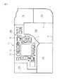
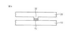
図2〜図4は配線基板にシールド板(パネル)を設けてシールドする従来例について説明する。図2はシールドパターンを形成した回路基板の平面図、図3は金属板等により成るシールド板(パネル)の平面図、図4はシールド板のパターン突起部と配線基板上のシールドパターンと間の接触部の断面図である。 2 to 4 illustrate a conventional example in which a shield plate (panel) is provided on a wiring board for shielding. FIG. 2 is a plan view of a circuit board on which a shield pattern is formed, FIG. 3 is a plan view of a shield board (panel) made of a metal plate, etc., and FIG. It is sectional drawing of a contact part.
配線基板10の表面には、図2に示すように、半導体素子等の各種の電子部品11が搭載されている。これらの電子部品の中に基板搭載型のインダクタ12も含まれる。配線基板10の表面には、回路ブロック13a、13b、13c、・・・毎に、同ブロックを1つの領域としてその周囲を連続して囲む導体のシールドパターン14が形成されている。なお、図2では、便宜上1つの回路ブロック13a内のみ搭載されている電子部品11を概略的に図示し、他の回路ブロック13b、13c、・・・内に搭載されている電子部品については図示を省略している。 As shown in FIG. 2, various
例えば導電体である金属板よりなるシールドパネル20は、図2に示すように、配線基板10の回路ブロック13a、13b、13c、・・・に対応する各ブロック21a、21b、21c、・・・毎にそれぞれその周囲を連続して囲む、配線基板10の導体シールドパターン14に対応する凸状のパターン22を有する。このようなシールドパネル20は配線基板10と接合され、配線基板10のシールドパターン14がシールドパネル20の凸状のパターン22に接触する。これにより、配線基板10は回路ブロック13毎にシールドパネル20によりシールドされることとなる。 For example, as shown in FIG. 2, the
特許文献1及び2に開示されている従来のインダクタ内蔵型配線基板では、上述のように、プリント配線基板上に所望のインダクタンス値のコイルを形成することが可能となる。しかしながら、プリント配線基板上でコイルを形成する場合のパターン作成面積、インダクタンス値、共振周波数等の主たる要因により十分合理的に満足できるインダクタを得ることは困難であった。 In the conventional inductor-embedded wiring board disclosed in
即ち、特許文献1及び2に開示されているインダクタ内蔵型配線基板においては、配線基板に占めるインダクタの占有面積が大きくなり、その結果、配線基板の配線密度が低下したり、他の部品等も含めた配線基板の実装密度が低下する原因となっていた。 That is, in the inductor-embedded wiring board disclosed in
そこで、本発明では、配線基板上にパターン形成するインダクタにおいて、図2〜図4において説明したようなシールド構造を利用してインダクタを形成することにより、配線スペースの有効活用を図り、配線基板上にコイルを形成してインダクタを得る場合のパターン作成面積を極力小さくし、且つ所望のインダクタンスの値を得、且つ共振周波数の高周波数化に対応可能なインダクタ内蔵型の配線基板を提供することを課題とする。 Therefore, in the present invention, in the inductor for pattern formation on the wiring board, the inductor is formed using the shield structure as described in FIGS. To provide a wiring board with a built-in inductor that can minimize the pattern creation area when obtaining an inductor by forming a coil on the surface, obtain a desired inductance value, and cope with a higher resonance frequency. Let it be an issue.
上記の課題を達成するために、本発明によれば、配線基板の表面上の少なくとも1つの電子部品搭載領域について、隣接する複数本の導体シールドパターンが前記配線基板の該領域の周囲を枠状に連続して囲むように形成し、該導体シールドパターン間の隙間に導体パターンからなるインダクタを形成したことを特徴とするシールド機能を有するインダクタ形成型配線基板が提供される。In order to achieve the above object, according to the present invention, for at least one electronic component mounting region on the surface of a wiring board,a plurality of adjacent conductor shield patterns form a frame around the area of the wiring substrate. formed so asto continuously surround, the inductor forming type wiring board having a shielding function, characterized in that the formation of the inductor comprising a conductor pattern on the gap between the conductor shield pattern isprovided.
2本の導体シールドパターン間の隙間に、1本のインダクタ用の導体パターンが、前記領域の周囲の全周にわたって連続して形成されていることを特徴とする。或いは、2本の導体シールドパターン間の隙間に、インダクタ用の導体パターンが、前記領域の周囲に途切れて形成され、非連続に形成されていることを特徴とする。 One conductor pattern for an inductor is formed continuously in the gap between two conductor shield patterns over the entire circumference of the region. Alternatively, the conductor pattern for the inductor is formed discontinuously around the region in the gap between the two conductor shield patterns, and is formed discontinuously.
上記のシールド機能を有するインダクタ内蔵型配線基板において、インダクタ用の導体パターンの表面は絶縁物に覆われていることを特徴とする。 In the inductor-embedded wiring board having the shield function, the surface of the conductor pattern for the inductor is covered with an insulator.
本発明はまた、電子部品を搭載した配線基板の表面上の少なくとも1つの領域について、隣接する複数本の導体シールドパターンが前記配線基板の該領域の周囲を枠状に連続して囲むように形成し、該導体シールドパターン間の隙間に導体パターンからなるインダクタを形成した配線基板と、前記複数本の導体シールドパターンに対応する輪郭を有し、該シールドパターンに接触する凸状パターンを有する少なくとも表面が導体からなるシールド板とで構成されたシールド機能を有するインダクタ形成型配線基板が提供される。In the present invention, for at least one region on the surface of the wiring board on which the electronic component is mounted,a plurality of adjacent conductor shield patterns are formedso as to continuously surround the periphery of the region of the wiring board in a frame shape. And at least a surface having a contour corresponding to the plurality of conductor shield patterns and having a convex pattern in contact with the shield patterns. There is provided an inductor-forming wiring board having a shielding function constituted by a shield plate made of a conductor.
本発明によれば、配線基板には、表面上の少なくとも1つの領域についてその周囲を枠状に連続して囲む導体シールドパターンを複数本互いに隣接して形成し、該導体シールドパターン間の隙間に導体パターンからなるインダクタを形成した構造を有する。また一方で、シールドパネルは、配線基板の前記複数本の導体シールドパターンに対応する輪郭を有し、該シールドパターンに接触する凸状パターンを有する少なくとも表面が金属からなる。したがって、シールドパネルの凸状パターンを配線基板の導体シールドパターンに接合させることにより、配線基板自体でシールド機能を有することとなり、配線基板に形成されたインダクタ自体もシールドされ、これにより、インダクタによるノイズを他の電子部品に発生させることなく、また、インダクタに必要な面積を確保しやすく、このためにインダクタンス値を大きくとることができる。 According to the present invention, on the wiring board, a plurality of conductor shield patterns that continuously surround the periphery of at least one region on the surface in a frame shape are formed adjacent to each other, and the gap between the conductor shield patterns is formed. It has a structure in which an inductor made of a conductor pattern is formed. On the other hand, the shield panel has a contour corresponding to the plurality of conductor shield patterns of the wiring board, and at least the surface having a convex pattern in contact with the shield pattern is made of metal. Therefore, by bonding the convex pattern of the shield panel to the conductor shield pattern of the wiring board, the wiring board itself has a shielding function, and the inductor itself formed on the wiring board is also shielded. Therefore, it is easy to secure a necessary area for the inductor without generating the same in other electronic components, and the inductance value can be increased.
以下、添付図面を参照して本発明の実施形態を詳細に説明する。 Hereinafter, embodiments of the present invention will be described in detail with reference to the accompanying drawings.
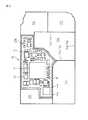
図5は本発明のシールド機能を有するインダクタ形成型配線基板の平面図である。図6はシールドパターン及びインダクタの配線のみを示す平面図である。 FIG. 5 is a plan view of an inductor-forming wiring board having a shield function according to the present invention. FIG. 6 is a plan view showing only the shield pattern and the wiring of the inductor.
配線基板10の表面には、図5に示すように、半導体素子等の各種の電子部品11が搭載されている。これらの電子部品の中に基板搭載型のインダクタ12が含まれても良い。配線基板10の表面には、回路ブロック13a、13b、13c、・・・毎に、同ブロックを1つの領域としてその周囲を連続して囲む導体のシールドパターン14a、14bが複数本、図示の実施形態では2本隣接して形成されている。これらの内周及び外周の2本の導体シールドパターン14a、14bは、例えば、領域13aの周囲を途切れることなく連続してつながっていて、同領域13aを枠状に完全に覆っている。また、2本の導体シールドパターン14a、14bは、その間に、後述するインダクタを構成する導体パターン16を配線できるように、略等幅の隙間を規定するように形成されている。 As shown in FIG. 5, various
なお、図5では、便宜上1つの回路ブロック13a内のみ搭載されている電子部品11を概略的に図示し、他の回路ブロック13b、13c、・・・内に搭載されている電子部品については図示を省略している。同様に、他の回路ブロック13b、13c、・・・の周囲にも、複数本の導体のシールドパターンが連続して枠状に形成されているが、図示を簡略化してある。なお、隣接する回路ブロックでは、2本の導体シールドパターン14a、14bの内の外周シールドパターン14bは相互に共用していても良い。 In FIG. 5, for convenience, the
2本の導体シールドパターン14a、14b間の隙間には、その中央にこれらのシールドパターン14a、14bと略平行に延びるインダクタを構成する導体パターン16が形成されている。図5及び図6の実施形態では、インダクタの導体パターン16は、回路ブロック13aの周囲枠の全周にわたって連続して形成されている。 In the gap between the two
図7は本発明によるシールド板(パネル)20の平面図である。このシールドパネル20は、従来と同様、例えば導体である金属板又は表面を導体金属によりめっき等で被覆した樹脂板よりなる。シールドパネル20は、図7に示すように、配線基板10の回路ブロック13a、13b、13c、・・・に対応する各ブロック21a、21b、21c、・・・毎にそれぞれその周囲を連続して囲む、配線基板10の複数本からなる導体シールドパターン14a、14bに対応する輪郭をもった複数本、この実施形態では2本の凸状のパターン22a、22bを有する。 FIG. 7 is a plan view of a shield plate (panel) 20 according to the present invention. The
なお、図7では、便宜上1つの回路ブロック13aに対応するシールドパネル20の領域ブロック21aのみ、2本の凸状のパターン22a、22bを示しているが、他の領域ブロック21b、21c、・・・の周囲にも、同様に、2本の凸状のパターンが形成されている。また、配線基板10の隣接する回路ブロックにおいて、外周側のシールドパターン14bが相互に共用している場合は、シールドパネル20も同様に、領域ブロックの外周側の凸状のパターン22bを相互に共用のものとする。 In FIG. 7, for convenience, only the
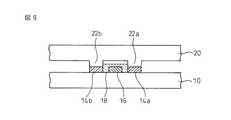
図8及び図9はシールドパネル20の凸状のパターン22a、22bと配線基板10上のシールドパターン14a、14bとの間の接触部の断面図である。シールドパネル20は配線基板10と接合され、配線基板10の2本のシールドパターン14a、14bがシールドパネル20の2本の凸状パターン22a、22bに接触する。これにより、配線基板10は各回路ブロック13a、13b、13c、・・・毎にシールドパネル20によりシールドされることとなる。 8 and 9 are cross-sectional views of contact portions between the
図8の実施形態では、インダクタの導体パターン16が配線基板10上に露出しているが、図9の実施形態のように、インダクタの導体パターン16を絶縁物18、例えソルダレジスト等で被覆し、インダクタ16を保護するようにしても良い。 In the embodiment of FIG. 8, the
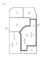
図10は本発明のシールド機能を有するインダクタ形成型配線基板の他の実施形態の平面図である。図10では、配線基板10の半導体素子等の各種の電子部品11が搭載されている1つの回路ブロック13aのみを示し、他の回路ブロックについては図示を省略してある。この実施形態では、各回路ブロックの周囲を連続して囲む導体のシールドパターン14a、14bが2本隣接して形成されている点は、図5に示す実施形態と同様であるが、2本のシールドパターン14a、14b間の隙間に形成されているインダクタを構成する導体パターン17は、回路ブロック13aの周囲枠の全周にわたって連続して形成されているのではなく、途中で途切れている。このような途切れたインダクタの導体パターン17a、17b、・・・は2本のシールドパターン14a、14b間の隙間の略中央にこれらと略平行に延びている点は、前述の実施形態の場合と同様である。 FIG. 10 is a plan view of another embodiment of the inductor-forming wiring board having a shielding function of the present invention. In FIG. 10, only one
各インダクタの導体パターン17a、17b、・・・の端部は、例えばスルーホール又は層間バイヤを介して、他の層に形成されているインダクタの導体パターン(図示せず)に接続されて適切なコイルを形成するようにしても良い。 The end portions of the
以上添付図面を参照して本発明の実施形態について説明したが、本発明は上記の実施形態に限定されるものではなく、本発明の精神ないし範囲内において種々の形態、変形、修正等が可能である。 Although the embodiments of the present invention have been described above with reference to the accompanying drawings, the present invention is not limited to the above-described embodiments, and various forms, modifications, corrections, and the like are possible within the spirit and scope of the present invention. It is.
例えば、上述の実施形態では、シールドパターン14a、14bを2本略平行して設けたが、このようなシールドパターンを3本以上略平行に配線し、それぞれ隣接するシールドパターン間の隙間に、1本ずつの連続又は非連続のインダクタ用の導体パターン16、17を設けることもできる。また、2本のシールドパターン14a、14b間の隙間に、2本以上の連続又は非連続のインダクタ用の導体パターン16、17を設けることも可能である。その他必要なインダクタンス値、その他の要因による仕様に応じて適宜の配線構造を選択することができる。 For example, in the above-described embodiment, two
以上説明したように、本発明によれば、配線基板には、表面上の少なくとも1つの領域についてその周囲を枠状に連続して囲む導体シールドパターンを複数本互いに隣接して形成し、該導体シールドパターン間の隙間に導体パターンからなるインダクタを形成した構造を有する。このため、シールド板の凸状パターンを配線基板のシールドパターンに接合させることにより、インダクタ自体がシールドされ、インダクタによるノイズを他の電子部品に発生させることなく、また、インダクタに必要な面積を確保しやすく、このためにインダクタンス値を大きくとることができる。従って、このようなシールド機能を有するインダクタ形成型配線基板は、携帯電話、パーソナルコンピュータ、携帯端末、PDA、自動車の制御装置、小型通信機器、小型ゲーム機等にインダクタ内蔵型の配線基板として利用することができる。 As described above, according to the present invention, on the wiring board, a plurality of conductor shield patterns that continuously surround the periphery of at least one region on the surface in a frame shape are formed adjacent to each other. It has a structure in which an inductor made of a conductor pattern is formed in a gap between shield patterns. For this reason, by joining the convex pattern of the shield plate to the shield pattern of the wiring board, the inductor itself is shielded, so that noise caused by the inductor is not generated in other electronic components and the necessary area for the inductor is secured. For this reason, the inductance value can be increased. Therefore, the inductor-forming wiring board having such a shielding function is used as a wiring board with a built-in inductor in a mobile phone, a personal computer, a portable terminal, a PDA, an automobile control device, a small communication device, a small game machine, and the like. be able to.
10 配線基板
11 電子部品(半導体素子)
12 基板搭載型インダクタ
13a〜13f 回路ブロックの内側端部
14a、14b シールドパターン
16、17 インダクタの導体パターン
20 シールド板(パネル)
21a〜21f 領域ブロック
22a、22b 凸状パターン10
DESCRIPTION OF
21a-21f
Claims (5)
Translated fromJapanesePriority Applications (2)
| Application Number | Priority Date | Filing Date | Title |
|---|---|---|---|
| JP2007175514AJP5041897B2 (en) | 2007-07-03 | 2007-07-03 | Inductor-formed wiring board with shielding function |
| US12/165,885US7929320B2 (en) | 2007-07-03 | 2008-07-01 | Inductor built-in wiring board having shield function |
Applications Claiming Priority (1)
| Application Number | Priority Date | Filing Date | Title |
|---|---|---|---|
| JP2007175514AJP5041897B2 (en) | 2007-07-03 | 2007-07-03 | Inductor-formed wiring board with shielding function |
Publications (2)
| Publication Number | Publication Date |
|---|---|
| JP2009016501A JP2009016501A (en) | 2009-01-22 |
| JP5041897B2true JP5041897B2 (en) | 2012-10-03 |
Family
ID=40220576
Family Applications (1)
| Application Number | Title | Priority Date | Filing Date |
|---|---|---|---|
| JP2007175514AActiveJP5041897B2 (en) | 2007-07-03 | 2007-07-03 | Inductor-formed wiring board with shielding function |
Country Status (2)
| Country | Link |
|---|---|
| US (1) | US7929320B2 (en) |
| JP (1) | JP5041897B2 (en) |
Families Citing this family (24)
| Publication number | Priority date | Publication date | Assignee | Title |
|---|---|---|---|---|
| US7065658B1 (en) | 2001-05-18 | 2006-06-20 | Palm, Incorporated | Method and apparatus for synchronizing and recharging a connector-less portable computer system |
| USD640976S1 (en) | 2008-08-28 | 2011-07-05 | Hewlett-Packard Development Company, L.P. | Support structure and/or cradle for a mobile computing device |
| US8401469B2 (en)* | 2008-09-26 | 2013-03-19 | Hewlett-Packard Development Company, L.P. | Shield for use with a computing device that receives an inductive signal transmission |
| US8712324B2 (en) | 2008-09-26 | 2014-04-29 | Qualcomm Incorporated | Inductive signal transfer system for computing devices |
| US8527688B2 (en)* | 2008-09-26 | 2013-09-03 | Palm, Inc. | Extending device functionality amongst inductively linked devices |
| US8868939B2 (en) | 2008-09-26 | 2014-10-21 | Qualcomm Incorporated | Portable power supply device with outlet connector |
| US8234509B2 (en)* | 2008-09-26 | 2012-07-31 | Hewlett-Packard Development Company, L.P. | Portable power supply device for mobile computing devices |
| US8688037B2 (en)* | 2008-09-26 | 2014-04-01 | Hewlett-Packard Development Company, L.P. | Magnetic latching mechanism for use in mating a mobile computing device to an accessory device |
| US8850045B2 (en) | 2008-09-26 | 2014-09-30 | Qualcomm Incorporated | System and method for linking and sharing resources amongst devices |
| US20110106954A1 (en)* | 2008-09-26 | 2011-05-05 | Manjirnath Chatterjee | System and method for inductively pairing devices to share data or resources |
| US8385822B2 (en)* | 2008-09-26 | 2013-02-26 | Hewlett-Packard Development Company, L.P. | Orientation and presence detection for use in configuring operations of computing devices in docked environments |
| US9083686B2 (en)* | 2008-11-12 | 2015-07-14 | Qualcomm Incorporated | Protocol for program during startup sequence |
| WO2010078557A2 (en)* | 2009-01-05 | 2010-07-08 | Palm, Inc. | Interior connector scheme for accessorizing a mobile computing device with a removeable housing segment |
| US9395827B2 (en)* | 2009-07-21 | 2016-07-19 | Qualcomm Incorporated | System for detecting orientation of magnetically coupled devices |
| US8954001B2 (en)* | 2009-07-21 | 2015-02-10 | Qualcomm Incorporated | Power bridge circuit for bi-directional wireless power transmission |
| US8437695B2 (en)* | 2009-07-21 | 2013-05-07 | Hewlett-Packard Development Company, L.P. | Power bridge circuit for bi-directional inductive signaling |
| US8755815B2 (en) | 2010-08-31 | 2014-06-17 | Qualcomm Incorporated | Use of wireless access point ID for position determination |
| US8395547B2 (en) | 2009-08-27 | 2013-03-12 | Hewlett-Packard Development Company, L.P. | Location tracking for mobile computing device |
| USD674391S1 (en) | 2009-11-17 | 2013-01-15 | Hewlett-Packard Development Company, L.P. | Docking station for a computing device |
| CN103222319B (en) | 2010-09-29 | 2016-08-10 | 高通股份有限公司 | A kind of method for mobile computing device and mobile computing device |
| US9685425B2 (en)* | 2014-01-28 | 2017-06-20 | Apple Inc. | Integrated circuit package |
| CN109741928B (en)* | 2018-11-29 | 2021-01-15 | 深圳市信维通信股份有限公司 | Manufacturing method of magnetic field shielding sheet and terminal |
| CN113301707B (en)* | 2020-02-24 | 2022-09-27 | 北京小米移动软件有限公司 | A circuit board and terminal equipment |
| JP7456829B2 (en)* | 2020-03-27 | 2024-03-27 | ラピスセミコンダクタ株式会社 | Shield case and electronic circuit module |
Family Cites Families (15)
| Publication number | Priority date | Publication date | Assignee | Title |
|---|---|---|---|---|
| US5014160A (en)* | 1989-07-05 | 1991-05-07 | Digital Equipment Corporation | EMI/RFI shielding method and apparatus |
| JPH0494196A (en)* | 1990-08-09 | 1992-03-26 | Toshiba Corp | Electronic circuit board |
| JPH0521979A (en)* | 1991-07-12 | 1993-01-29 | Fujitsu Ltd | Printed board shield structure |
| JP3212657B2 (en) | 1991-12-26 | 2001-09-25 | シャープ株式会社 | Printed circuit board |
| JP3651995B2 (en)* | 1996-01-29 | 2005-05-25 | 本田技研工業株式会社 | Impedance matching device for glass antenna |
| JPH10223997A (en)* | 1997-02-12 | 1998-08-21 | Canon Inc | Printed wiring board |
| DK0910233T3 (en)* | 1997-10-13 | 2002-10-14 | Itt Mfg Enterprises Inc | Shielded PC Card and manufacturing process |
| JP3787436B2 (en)* | 1998-07-14 | 2006-06-21 | キヤノン株式会社 | Printed wiring board |
| JP2001077538A (en) | 1999-09-02 | 2001-03-23 | Fuji Photo Film Co Ltd | Pattern coil on printed board |
| US20050205292A1 (en)* | 2004-03-18 | 2005-09-22 | Etenna Corporation. | Circuit and method for broadband switching noise suppression in multilayer printed circuit boards using localized lattice structures |
| JP4771397B2 (en)* | 2004-04-15 | 2011-09-14 | ミツミ電機株式会社 | Electronics |
| JP2006100489A (en)* | 2004-09-29 | 2006-04-13 | Ricoh Co Ltd | Printed circuit board, electronic unit using the printed circuit board, and method for forming resin outflow prevention dam |
| JP2006294889A (en)* | 2005-04-12 | 2006-10-26 | Sony Corp | Circuit component formation |
| JP4701896B2 (en)* | 2005-07-21 | 2011-06-15 | 株式会社村田製作所 | Multilayer wiring board and manufacturing method thereof |
| US7310067B1 (en)* | 2006-05-23 | 2007-12-18 | Research In Motion Limited | Mobile wireless communications device with reduced interfering RF energy into RF metal shield secured on circuit board |
- 2007
- 2007-07-03JPJP2007175514Apatent/JP5041897B2/enactiveActive
- 2008
- 2008-07-01USUS12/165,885patent/US7929320B2/enactiveActive
Also Published As
| Publication number | Publication date |
|---|---|
| US7929320B2 (en) | 2011-04-19 |
| JP2009016501A (en) | 2009-01-22 |
| US20090008148A1 (en) | 2009-01-08 |
Similar Documents
| Publication | Publication Date | Title |
|---|---|---|
| JP5041897B2 (en) | Inductor-formed wiring board with shielding function | |
| JP6766740B2 (en) | Printed circuit board and switching regulator | |
| JP4802615B2 (en) | LC composite parts | |
| JP2012235080A (en) | Chip-type coil component | |
| JP2012235080A5 (en) | ||
| JP5356520B2 (en) | Wiring board, filter device and portable device | |
| CN107452460B (en) | Electronic component | |
| JP2007165483A (en) | Multilayer printed circuit board | |
| JP2009016504A (en) | Multilayer wiring board with built-in inductor | |
| US8004382B2 (en) | Inductor device, and method of manufacturing the same | |
| JPWO2020071493A1 (en) | module | |
| JP2013207149A (en) | Toroidal coil | |
| JP6029814B2 (en) | Chip inductor | |
| JP5716391B2 (en) | Coil built-in board | |
| JP6460290B2 (en) | DC / DC converter module | |
| JP5172311B2 (en) | Semiconductor module and portable device | |
| JP2018006437A (en) | Composite device | |
| JP5336127B2 (en) | Circuit board | |
| JP6264721B2 (en) | Multi-layer wiring board heat dissipation structure | |
| JP7736428B2 (en) | Substrate coil and transformer | |
| JP6083143B2 (en) | Chip inductor built-in wiring board | |
| KR20190111867A (en) | Flexible coil, and method of manufacturing the same, electronic component including flexible coil | |
| JP6343871B2 (en) | Component mounting multilayer wiring board | |
| JP4714300B2 (en) | Printed wiring board | |
| JP2008177363A (en) | Multilayer printed wiring board |
Legal Events
| Date | Code | Title | Description |
|---|---|---|---|
| A621 | Written request for application examination | Free format text:JAPANESE INTERMEDIATE CODE: A621 Effective date:20100427 | |
| A977 | Report on retrieval | Free format text:JAPANESE INTERMEDIATE CODE: A971007 Effective date:20111019 | |
| A131 | Notification of reasons for refusal | Free format text:JAPANESE INTERMEDIATE CODE: A131 Effective date:20111025 | |
| A521 | Request for written amendment filed | Free format text:JAPANESE INTERMEDIATE CODE: A523 Effective date:20111220 | |
| TRDD | Decision of grant or rejection written | ||
| A01 | Written decision to grant a patent or to grant a registration (utility model) | Free format text:JAPANESE INTERMEDIATE CODE: A01 Effective date:20120612 | |
| A01 | Written decision to grant a patent or to grant a registration (utility model) | Free format text:JAPANESE INTERMEDIATE CODE: A01 | |
| A61 | First payment of annual fees (during grant procedure) | Free format text:JAPANESE INTERMEDIATE CODE: A61 Effective date:20120710 | |
| R150 | Certificate of patent or registration of utility model | Ref document number:5041897 Country of ref document:JP Free format text:JAPANESE INTERMEDIATE CODE: R150 Free format text:JAPANESE INTERMEDIATE CODE: R150 | |
| FPAY | Renewal fee payment (event date is renewal date of database) | Free format text:PAYMENT UNTIL: 20150720 Year of fee payment:3 |